JP2006507662A - Arc suppression method and system in plasma processing system - Google Patents
Arc suppression method and system in plasma processing systemDownload PDFInfo
- Publication number
- JP2006507662A JP2006507662AJP2004517580AJP2004517580AJP2006507662AJP 2006507662 AJP2006507662 AJP 2006507662AJP 2004517580 AJP2004517580 AJP 2004517580AJP 2004517580 AJP2004517580 AJP 2004517580AJP 2006507662 AJP2006507662 AJP 2006507662A
- Authority
- JP
- Japan
- Prior art keywords
- signal
- plasma processing
- processing system
- plasma
- antenna
- Prior art date
- Legal status (The legal status is an assumption and is not a legal conclusion. Google has not performed a legal analysis and makes no representation as to the accuracy of the status listed.)
- Pending
Links
- 238000012545processingMethods0.000titleclaimsabstractdescription128
- 238000000034methodMethods0.000titleclaimsabstractdescription104
- 230000001629suppressionEffects0.000titleclaimsabstractdescription44
- 239000000758substrateSubstances0.000claimsabstractdescription70
- 230000008569processEffects0.000claimsabstractdescription53
- 238000005259measurementMethods0.000claimsdescription21
- 239000004020conductorSubstances0.000claimsdescription17
- 239000000523sampleSubstances0.000claimsdescription7
- WABPQHHGFIMREM-UHFFFAOYSA-Nlead(0)Chemical compound[Pb]WABPQHHGFIMREM-UHFFFAOYSA-N0.000claimsdescription6
- 238000012986modificationMethods0.000claimsdescription4
- 230000004048modificationEffects0.000claimsdescription4
- 230000008878couplingEffects0.000claimsdescription2
- 238000010168coupling processMethods0.000claimsdescription2
- 238000005859coupling reactionMethods0.000claimsdescription2
- 238000001914filtrationMethods0.000claims9
- 230000015572biosynthetic processEffects0.000claims2
- 239000007789gasSubstances0.000description27
- 239000000463materialSubstances0.000description12
- 238000002347injectionMethods0.000description9
- 239000007924injectionSubstances0.000description9
- 238000010586diagramMethods0.000description6
- 230000006698inductionEffects0.000description6
- 238000005530etchingMethods0.000description5
- 239000000919ceramicSubstances0.000description4
- HBMJWWWQQXIZIP-UHFFFAOYSA-Nsilicon carbideChemical compound[Si+]#[C-]HBMJWWWQQXIZIP-UHFFFAOYSA-N0.000description4
- 229910010271silicon carbideInorganic materials0.000description4
- 238000012546transferMethods0.000description4
- 229910052782aluminiumInorganic materials0.000description3
- XAGFODPZIPBFFR-UHFFFAOYSA-NaluminiumChemical compound[Al]XAGFODPZIPBFFR-UHFFFAOYSA-N0.000description3
- PNEYBMLMFCGWSK-UHFFFAOYSA-Naluminium oxideInorganic materials[O-2].[O-2].[O-2].[Al+3].[Al+3]PNEYBMLMFCGWSK-UHFFFAOYSA-N0.000description3
- 238000005229chemical vapour depositionMethods0.000description3
- 238000013461designMethods0.000description3
- 238000010438heat treatmentMethods0.000description3
- 238000009616inductively coupled plasmaMethods0.000description3
- 150000002500ionsChemical class0.000description3
- 238000004519manufacturing processMethods0.000description3
- 239000010453quartzSubstances0.000description3
- 229910052710siliconInorganic materials0.000description3
- 239000010703siliconSubstances0.000description3
- VYPSYNLAJGMNEJ-UHFFFAOYSA-Nsilicon dioxideInorganic materialsO=[Si]=OVYPSYNLAJGMNEJ-UHFFFAOYSA-N0.000description3
- XKRFYHLGVUSROY-UHFFFAOYSA-NArgonChemical compound[Ar]XKRFYHLGVUSROY-UHFFFAOYSA-N0.000description2
- RYGMFSIKBFXOCR-UHFFFAOYSA-NCopperChemical compound[Cu]RYGMFSIKBFXOCR-UHFFFAOYSA-N0.000description2
- XEEYBQQBJWHFJM-UHFFFAOYSA-NIronChemical compound[Fe]XEEYBQQBJWHFJM-UHFFFAOYSA-N0.000description2
- PXHVJJICTQNCMI-UHFFFAOYSA-NNickelChemical compound[Ni]PXHVJJICTQNCMI-UHFFFAOYSA-N0.000description2
- 238000006243chemical reactionMethods0.000description2
- 238000001816coolingMethods0.000description2
- 229910052802copperInorganic materials0.000description2
- 239000010949copperSubstances0.000description2
- 238000009826distributionMethods0.000description2
- 230000004907fluxEffects0.000description2
- 239000000203mixtureSubstances0.000description2
- 238000012544monitoring processMethods0.000description2
- 238000005240physical vapour depositionMethods0.000description2
- 239000004065semiconductorSubstances0.000description2
- 239000000126substanceSubstances0.000description2
- WFKWXMTUELFFGS-UHFFFAOYSA-NtungstenChemical compound[W]WFKWXMTUELFFGS-UHFFFAOYSA-N0.000description2
- 229910052721tungstenInorganic materials0.000description2
- 239000010937tungstenSubstances0.000description2
- 229910018072Al 2 O 3Inorganic materials0.000description1
- BSYNRYMUTXBXSQ-UHFFFAOYSA-NAspirinChemical compoundCC(=O)OC1=CC=CC=C1C(O)=OBSYNRYMUTXBXSQ-UHFFFAOYSA-N0.000description1
- 229910052582BNInorganic materials0.000description1
- PZNSFCLAULLKQX-UHFFFAOYSA-NBoron nitrideChemical compoundN#BPZNSFCLAULLKQX-UHFFFAOYSA-N0.000description1
- OKTJSMMVPCPJKN-UHFFFAOYSA-NCarbonChemical compound[C]OKTJSMMVPCPJKN-UHFFFAOYSA-N0.000description1
- VYZAMTAEIAYCRO-UHFFFAOYSA-NChromiumChemical compound[Cr]VYZAMTAEIAYCRO-UHFFFAOYSA-N0.000description1
- 239000004642PolyimideSubstances0.000description1
- 229910004298SiO 2Inorganic materials0.000description1
- XUIMIQQOPSSXEZ-UHFFFAOYSA-NSiliconChemical compound[Si]XUIMIQQOPSSXEZ-UHFFFAOYSA-N0.000description1
- 229910045601alloyInorganic materials0.000description1
- 239000000956alloySubstances0.000description1
- 238000002048anodisation reactionMethods0.000description1
- 229910052786argonInorganic materials0.000description1
- 229910052799carbonInorganic materials0.000description1
- 238000005266castingMethods0.000description1
- 229910052804chromiumInorganic materials0.000description1
- 239000011651chromiumSubstances0.000description1
- 239000011248coating agentSubstances0.000description1
- 238000000576coating methodMethods0.000description1
- 238000004891communicationMethods0.000description1
- 239000002826coolantSubstances0.000description1
- PMHQVHHXPFUNSP-UHFFFAOYSA-Mcopper(1+);methylsulfanylmethane;bromideChemical compoundBr[Cu].CSCPMHQVHHXPFUNSP-UHFFFAOYSA-M0.000description1
- 230000007423decreaseEffects0.000description1
- 238000000151depositionMethods0.000description1
- 230000008021depositionEffects0.000description1
- 238000005137deposition processMethods0.000description1
- 239000003989dielectric materialSubstances0.000description1
- 238000010292electrical insulationMethods0.000description1
- 238000005516engineering processMethods0.000description1
- 239000011521glassSubstances0.000description1
- 239000002241glass-ceramicSubstances0.000description1
- 238000009413insulationMethods0.000description1
- 229910052742ironInorganic materials0.000description1
- 239000004973liquid crystal related substanceSubstances0.000description1
- 229910003465moissaniteInorganic materials0.000description1
- 229910052759nickelInorganic materials0.000description1
- 235000012771pancakesNutrition0.000description1
- 238000009931pascalizationMethods0.000description1
- 230000036470plasma concentrationEffects0.000description1
- 238000001020plasma etchingMethods0.000description1
- 229920001721polyimidePolymers0.000description1
- 230000001902propagating effectEffects0.000description1
- 238000005086pumpingMethods0.000description1
- 230000003134recirculating effectEffects0.000description1
- 238000005245sinteringMethods0.000description1
- 239000010409thin filmSubstances0.000description1
- 238000007740vapor depositionMethods0.000description1
- 238000003466weldingMethods0.000description1
Images


Classifications
- H—ELECTRICITY
- H01—ELECTRIC ELEMENTS
- H01J—ELECTRIC DISCHARGE TUBES OR DISCHARGE LAMPS
- H01J37/00—Discharge tubes with provision for introducing objects or material to be exposed to the discharge, e.g. for the purpose of examination or processing thereof
- H01J37/32—Gas-filled discharge tubes
- H01J37/32009—Arrangements for generation of plasma specially adapted for examination or treatment of objects, e.g. plasma sources
- H01J37/32082—Radio frequency generated discharge
- H01J37/32174—Circuits specially adapted for controlling the RF discharge
- H—ELECTRICITY
- H01—ELECTRIC ELEMENTS
- H01J—ELECTRIC DISCHARGE TUBES OR DISCHARGE LAMPS
- H01J37/00—Discharge tubes with provision for introducing objects or material to be exposed to the discharge, e.g. for the purpose of examination or processing thereof
- H01J37/32—Gas-filled discharge tubes
- H01J37/32431—Constructional details of the reactor
- H01J37/32697—Electrostatic control
- H01J37/32706—Polarising the substrate
- H—ELECTRICITY
- H01—ELECTRIC ELEMENTS
- H01J—ELECTRIC DISCHARGE TUBES OR DISCHARGE LAMPS
- H01J37/00—Discharge tubes with provision for introducing objects or material to be exposed to the discharge, e.g. for the purpose of examination or processing thereof
- H01J37/32—Gas-filled discharge tubes
- H01J37/32917—Plasma diagnostics
- H01J37/32935—Monitoring and controlling tubes by information coming from the object and/or discharge
- H—ELECTRICITY
- H01—ELECTRIC ELEMENTS
- H01J—ELECTRIC DISCHARGE TUBES OR DISCHARGE LAMPS
- H01J2237/00—Discharge tubes exposing object to beam, e.g. for analysis treatment, etching, imaging
- H01J2237/02—Details
- H01J2237/0203—Protection arrangements
- H01J2237/0206—Extinguishing, preventing or controlling unwanted discharges
Landscapes
- Physics & Mathematics (AREA)
- Engineering & Computer Science (AREA)
- Plasma & Fusion (AREA)
- Chemical & Material Sciences (AREA)
- Analytical Chemistry (AREA)
- Chemical Vapour Deposition (AREA)
- Plasma Technology (AREA)
- Physical Vapour Deposition (AREA)
- Drying Of Semiconductors (AREA)
Abstract
Translated fromJapaneseDescription
Translated fromJapanese (関連出願の相互参照)
本願は、2002年6月28日出願の米国特許出願第60/391,950号に対し優先権を主張しており、また本願は、「RFプラズマシステム内のアーク発生を検出し、また阻止する装置および方法」と題する米国特許第6,332,961号に関連し、その全内容は参照してここに組み込まれる。(Cross-reference of related applications)
This application claims priority to US Patent Application No. 60 / 391,950 filed June 28, 2002, and this application “detects and prevents arcing in RF plasma systems. No. 6,332,961, entitled “Apparatus and Methods”, the entire contents of which are hereby incorporated by reference.
本発明は、プラズマ処理、より詳しくはプラズマ処理のためのアーク抑制システムおよびこれを使用する方法に関する。 The present invention relates to plasma processing, and more particularly to an arc suppression system for plasma processing and methods of using the same.
半導体工業における集積回路(IC)の製造は、一般的にプラズマを使用して基板から物質を除去し、また物質を蒸着するのに必要とするプラズマ反応装置内で界面化学反応を生成し、また補助する。概して、プラズマは真空条件下において電子を加熱して、供給処理ガスとのイオン化衝突に耐えるのに充分なエネルギーを与えることによって、プラズマ反応装置内で形成される。さらに、加熱電子は解離的衝突に耐えるに充分なエネルギーを有することができ、したがって所定条件(例えば、チャンバ圧、ガス流量等)下における一連の特定するガスが、帯電種の個体数およびチャンバ内で実行される特定処理(例えば、物質が基板から除去されるエッチング処理か、または物質が基板に付加される溶着処理)に適した化学的反応種を生成するように選択される。一般的に、エッチングを適用するようなプラズマ処理中、電荷が基板表面に渡って蓄積する恐れがある。しかし、基板帯電は基板表面に渡ってスペース的に不均質となる可能性がある。基板表面の不均質帯電は、スペース的な不均質プラズマと基板表面との接触のために生じることが観測されている。プラズマの不均質は、例えば不均質プラズマ発生または不均質プラズマ密度に起因する損失、または不均質イオンエネルギー(基板表面に衝突するイオンによる)に起因する基板周辺のプラズマ反応装置構造に関連する基板表面の、過度な不均質プラズマシースのせいである。これらの不均質の結果として、基板を横切る横方向アーク発生の危険性が、大きく高揚される。基板アーク発生は、許容可能な装置歩留まりを保つために完全に阻止しなければならない。 The manufacture of integrated circuits (ICs) in the semiconductor industry typically uses plasma to remove materials from a substrate and to generate interfacial chemical reactions within the plasma reactor required to deposit the materials, Assist. Generally, a plasma is formed in a plasma reactor by heating electrons under vacuum conditions to provide sufficient energy to withstand ionization collisions with the feed process gas. In addition, the heated electrons can have sufficient energy to withstand dissociative collisions, so a series of specific gases under predetermined conditions (eg, chamber pressure, gas flow rate, etc.) Are selected to produce chemically reactive species suitable for the particular process performed in (e.g., an etching process where the material is removed from the substrate or a deposition process where the material is added to the substrate). In general, charge may accumulate across the substrate surface during plasma processing, such as etching. However, substrate charging can be spatially inhomogeneous across the substrate surface. It has been observed that inhomogeneous charging of the substrate surface occurs due to contact between the spatially inhomogeneous plasma and the substrate surface. Plasma inhomogeneity is a substrate surface related to the plasma reactor structure around the substrate due to loss due to, for example, inhomogeneous plasma generation or inhomogeneous plasma density, or due to inhomogeneous ion energy (due to ions impinging on the substrate surface). This is due to the excessive inhomogeneous plasma sheath. As a result of these inhomogeneities, the risk of generating a transverse arc across the substrate is greatly enhanced. Substrate arcing must be completely prevented to maintain acceptable device yield.
本発明は、プラズマ処理システムのためのアーク抑制システムを提供し、プラズマ処理システムに結合された少なくとも1つのセンサと、少なくとも1つのセンサに結合されたコントローラを備え、このコントローラが少なくとも1つのセンサから発生された少なくとも1つの信号を使用してプラズマ処理システムの状態を決定することと、アーク事象発生を抑制するためにプラズマ処理システムを制御することのために少なくとも1つのアルゴリズムを提供する。 The present invention provides an arc suppression system for a plasma processing system, comprising: at least one sensor coupled to the plasma processing system; and a controller coupled to the at least one sensor, the controller from the at least one sensor. At least one algorithm is provided for determining the state of the plasma processing system using the generated at least one signal and for controlling the plasma processing system to suppress arc event occurrence.
本発明は、アーク抑制システムを利用してプラズマ処理システム内のアークを抑制するための方法をさらに提供し、この方法が少なくとも1つのセンサを使用してプラズマ処理システムに関する少なくとも1つの信号を測定する工程と、少なくとも1つの信号と接地電位間の少なくとも1つの差を決定する工程と、少なくとも1つの差信号を目標差と比較する工程と、この比較からプラズマ処理システムの状態を決定する工程とを備えている。 The present invention further provides a method for suppressing an arc in a plasma processing system utilizing an arc suppression system that uses at least one sensor to measure at least one signal for the plasma processing system. Determining at least one difference between at least one signal and ground potential; comparing at least one difference signal with a target difference; and determining the state of the plasma processing system from this comparison. I have.
本発明は、アーク抑制システムを利用してプラズマ処理システム内のアークを抑制するための方法をさらに提供し、この方法が第1のセンサを使用してプラズマ処理システムに関する第1の信号を測定する工程と、第2のセンサを使用してプラズマ処理システムに関する第2の信号を測定する工程と、第1の信号と第2の信号間の差信号を決定する工程と、第1の信号と前記第2の信号間の差信号を目標差と比較する工程と、この比較からプラズマ処理システムの状態を決定する工程とを備えている。 The present invention further provides a method for suppressing an arc in a plasma processing system utilizing an arc suppression system, the method using a first sensor to measure a first signal related to the plasma processing system. Measuring a second signal for the plasma processing system using a second sensor; determining a difference signal between the first signal and the second signal; the first signal; Comparing the difference signal between the second signals with a target difference and determining the state of the plasma processing system from this comparison.
本発明の別の目的は、アーク事象発生を抑制するためにプラズマ処理システムの状態により、プラズマ処理システムを制御する工程をさらに備えたアーク抑制システムを利用して、プラズマ処理システム内のアーク発生を抑制するための方法を提供することである。 Another object of the present invention is to suppress arc generation in a plasma processing system using an arc suppression system further comprising a step of controlling the plasma processing system according to the state of the plasma processing system in order to suppress the occurrence of an arc event. It is to provide a method for suppressing.
本発明のこれらのおよび他の利点は、添付図面に関して与えられた本発明の代表的な実施形態の次なる詳細な説明からより明白となり、またより容易に理解することができよう。 These and other advantages of the present invention will become more apparent and more readily understood from the following detailed description of exemplary embodiments of the invention given with reference to the accompanying drawings.
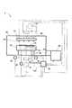
本発明の一実施形態に基づいて、プラズマ処理システム1を図1に示す。このシステムは処理反応装置10、基板25を支持する基板ホルダ20、アーク抑制システム100を備えており、このアーク抑制システム100は処理反応装置10に結合された少なくとも1つのセンサ50と、少なくとも1つのセンサ50に結合されたコントローラ55を備えている。さらに、コントローラ55は、少なくとも1つのセンサ50から発生された少なくとも1つの信号を使用してプラズマ処理システム1の状態を決定するための少なくとも1つのアルゴリズムを実行すること、アーク事象発生を抑制するためにプラズマ処理システム1を制御することが可能である。 In accordance with one embodiment of the present invention, a
本発明の一実施形態において、少なくとも1つのセンサ50が少なくとも1つのアンテナと、各アンテナに接続された電気測定装置56を備えることができる。別の実施形態において、少なくとも1つのアンテナが少なくとも1つのアンテナ電極52と、少なくとも1つのアンテナ電極52に接続されたアンテナリード線54を備えている。 In one embodiment of the present invention, at least one
例示の実施形態において、図1に示したプラズマ処理システム1は物質を処理するためにプラズマを利用する。望ましくは、プラズマ処理システム1はエッチングチャンバを備えている。別の方法として、プラズマ処理システム1は化学蒸着(CVD)システムまたは物理蒸着(PVD)システムのような溶着チャンバを備えることができる。 In the illustrated embodiment, the
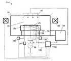
図2に示した本発明の例示の実施形態によれば、プラズマ処理システム1は処理反応装置10、その上に処理されるべき基板25が付着された基板ホルダ20、ガス注入システム40、真空ポンプシステム58を備えることができる。例えば、基板25は半導体基板、ウェハ、または液晶表示装置(LCD)とすることができる。例えば、処理反応装置10は、基板25の表面近傍の処理領域45内でプラズマの発生を容易にするように構成され、ここでプラズマが加熱電子とイオン化可能ガス間の衝突によって形成される。例えば、イオン化可能ガスまたはガスの混合物がガス注入システム40を介して導入することができ、また処理圧は真空ポンプシステム58を使用して調整することができる。望ましくは、プラズマは事前決定物質処理に対して特定する物質を生成するのに利用され、また物質を基板25に溶着するか、または基板25の露呈表面から物質を除去する。 According to the exemplary embodiment of the present invention shown in FIG. 2, the
例えば、基板25は静電クランプシステム28を介して基板ホルダ20に付着させることができる。さらに、基板ホルダ20は基板ホルダ20から熱を受け、また熱交換システム(図示せず)に熱を移送し、あるいは発熱したときに熱交換システムからの熱を移送する再循環冷却剤流を含む冷却システムをさらに含めることができる。さらに、ガスが裏面ガスシステム26を介して基板の背後に分配されて、基板25と基板ホルダ20間のガス−空隙熱コンダクタンスを改善することができる。この種のシステムは、温度の上昇または降下時において基板の温度制御が必要とされるときに、利用することができる。例えば、基板の温度制御は、プラズマから基板25に分配される熱流束と基板ホルダ20への伝導によって基板25から除去される熱流束のバランスのために達成される定常状態温度を超過した温度において有効となる。他の実施形態において、抵抗性発熱素子または熱電ヒーター/冷却装置のような発熱素子を含めることができる。 For example, the
図2に示した代表的実施形態において、基板ホルダ20はさらにRF電力が処理領域45内でプラズマに結合される電極としても作用する。例えば、基板ホルダ20はインピーダンスマッチネットワーク32を通してRF発生装置30から基板ホルダ20へRF電力の移送を介してRF電圧で電気的にバイアスすることができる。RFバイアスは電子を加熱する働きをし、これによってプラズマを形成および維持することができる。この構成において、システムはリアクティブイオンエッチング(RIE)反応装置として作動することができ、この装置のチャンバおよび上方ガス注入電極は接地面として作用する。RFバイアスの一般的な周波数は、1MHzから100MHzの範囲とすることができ、好ましくは13.56MHzである。プラズマ処理のためのRFシステムは、当業者にとって周知である。 In the exemplary embodiment shown in FIG. 2, the
別の方法として、RF電力は多周波周波数で基板ホルダ電極に印加することができる。さらに、インピーダンスマッチネットワーク32は、反射電力を最小化することによってプラズマ処理反応装置10へのRF電力の移送を最大化するように作用することができる。マッチネットワークトポロジー(例えば、L−タイプ、π―タイプ、T−タイプ等)および自動制御方法は、当業者にとって周知である。 Alternatively, RF power can be applied to the substrate holder electrode at multiple frequency frequencies. Furthermore, the
図2を引き続き参照して、処理ガスはガス注入システム40を介して処理領域45に導入することができる。例えば、処理ガスは酸化物エッチング適用に対してアルゴン、CF4およびO2またはアルゴン、C4F8およびO2のようなガスの混合物、またはO2/CO/Ar/C4F8、O2/CO/Ar/C5F8、O2/CO/Ar/C4F6、O2/Ar/C4F6、N2/H2のような他の化学物質を備えている。ガス注入システム40は、シャワーヘッドを備え、ここで処理ガスがガス分配システム(図示せず)からガス注入プレナム(図示せず)、一連のバッフル板(図示せず)および多数オリフィスシャワーヘッドガス注入板(図示せず)を介して処理領域45に供給される。ガス注入システムは当業者には周知である。With continued reference to FIG. 2, process gas may be introduced into
真空ポンプシステム58は、例えば、1秒当り5000リットルまで(およびこれ以上)吸い上げ速度を可能なターボ分子真空ポンプ(TMP)と、チャンバ圧を絞るためのゲート弁を含んでいる。ドライプラズマエッチングのために利用される従来のプラズマ処理装置において、1秒当り1000から3000リットルのTMPが一般的に使用される。TMPは低圧処理、一般に50mトル未満に有効である。これより高い圧力において、TMP吸い上げ速度は急激に低下する。高圧処理に対して(すなわち、100mトルよりも大きい)、機械的ブースタポンプおよびドライ荒引きポンプが使用できる。さらに、チャンバ圧をモニタする装置(図示せず)が、処理反応装置10に接続される。この圧力測定装置は、例えばマサチューセッツ州アンドーバー(Andover,MA)のMKS株式会社(MKS Instruments,Inc.)から市販されている、タイプ628Bバラトロン絶対容量マノメータとすることができる。 The
例えば、コントローラ55は、マイクロプロセッサ、メモリおよびデジタルI/Oポートを備えることができ、このポートはプラズマ処理システム1と連絡し、入力を促進すると共に、プラズマ処理システム1からの出力をモニタするのに充分な制御電圧を発生することが可能である。さらに、コントローラ55はRF発生装置30、インピーダンスマッチネットワーク32、ガス注入システム40、真空ポンプシステム58、裏面ガス分配システム26、静電クランプシステム28およびセンサ50にさらに接続され、情報交換される。メモリ内に記憶されたプログラムは、記憶処理レシピに基づいてプラズマ処理システム1の前記要素への入力を作動するように利用される。コントローラ55の一例には、テキサス州ダラス(Dallas,Texas)のデルコーポレーション(Dell Corporation)から市販されている、DELL PRECISION WORKSTATION 610(商標)がある。別の方法として、コントローラ55はデジタル信号プロセッサ(DSP)を備えることができる。 For example, the
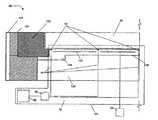
図3に示した代表的な実施形態において、プラズマ処理システム1は磁気フィールドシステム60をさらに備えることができる。例えば、磁気システム60は、潜在的にプラズマ濃度を増大させ、および/またはプラズマ処理均一性を改善するために、静止DC磁気フィールドシステムまたは、機械的または電気的回転DC磁気フィールドシステムを備えることができる。さらに、コントローラ55は、回転速度およびフィールド強度を調整するために、回転磁気フィールドシステムに接続することができる。回転磁気フィールドの設計および設定は当業者にとって周知である。 In the exemplary embodiment shown in FIG. 3, the
図4に示した代表的実施形態において、図1および2のプラズマ処理システム1が、上方電極70をさらに備えており、これにインピーダンスマッチネットワーク74を介してRF発生装置72が接続され、RF電力を供給することができる。上方電極へ供給されるRF電力の典型的な周波数は、10MHzから200MHzであり、また60MHzが好ましい。さらに、下方電極へ供給される典型的な周波数は、0.1MHzから30MHzであり、また2MHzが好ましい。さらに、コントローラ55は、上方電極70へのRF電力の供給を制御するために、RF発生装置72およびインピーダンスマッチネットワーク74に接続される。上方電極の設計および設定は当業者にとって周知である。 In the exemplary embodiment shown in FIG. 4, the
図5に示した代表的実施形態において、図1および2のプラズマ処理システムが、誘導コイル80をさらに備えており、これにインピーダンスマッチネットワーク84を介してRF発生装置82が接続され、RF電力を供給することができる。RF電力は、誘電窓(図示せず)を介して、誘導コイル80からプラズマ処理領域45に誘導結合されている。RF電力が誘導コイル80へ適用される場合の典型的な周波数は、10MHzから100MHzの範囲であり、13.56MHzが好ましい。同様にして、チャック電極への電力適用のための典型的な周波数は、0.1MHzから30MHzの範囲であり、また13.56MHzが好ましい。その上、スロット付きファラデーシールド(図示せず)が誘導コイル80とプラズマ間の容量性結合を減じるのに使用できる。さらに、コントローラ55は、誘導コイル80への電力供給を制御するために、インピーダンスマッチネットワーク84を介してRF発生装置82に接続される。別の実施形態において、誘導コイル80は、「スパイラル」コイルまたは「パンケーキ」コイルとすることができ、変圧器結合プラズマ(TCP)反応装置内の上部からプラズマ処理領域と連絡されている。誘導結合プラズマ(ICP)源および/または変圧器結合プラズマ(TCP)源の設計および実施は、当業者には周知である。 In the exemplary embodiment shown in FIG. 5, the plasma processing system of FIGS. 1 and 2 further comprises an
別の方法において、プラズマは電子サイクロトロン共鳴(ECR)を使用して形成することができる。なおも別の実施形態において、プラズマはヘリコン波の放出から形成される。さらに別の実施形態において、プラズマは伝播表面波から形成される。上述した各プラズマ源は当業者にとって周知である。 In another method, the plasma can be formed using electron cyclotron resonance (ECR). In yet another embodiment, the plasma is formed from helicon wave emissions. In yet another embodiment, the plasma is formed from propagating surface waves. Each plasma source described above is well known to those skilled in the art.
上述したように、アーク抑制システム100は処理反応装置10に結合された少なくとも1つのセンサ50と、少なくとも1つのセンサ50に結合されたコントローラ55を備えており、コントローラ55は少なくとも1つのセンサ50から発生された少なくとも1つの信号を使用してプラズマ処理システム1の状態を決定し、またアーク発生事象を抑制するためにプラズマ処理システム1を制御するための、少なくとも1つのアルゴリズムを実行することが可能である。次の説明において、アーク抑制システム100をより詳細に説明する。
ここで図6を参照して、基板ホルダ20の断面の分解図を示す。概して、基板ホルダ20は外部シールド122、絶縁リング124、基板25の下にあるRFバイアス可能電極126および基板25を取り囲んでいるフォーカス(集束)リング128を備えることができる。例えば、外部シールド122は、電気的に接地された導電性素子とすることができ、表面アノード化および/または表面コーティング(例えば、Y2O3)を施すか、またはこれを施さないアルミニウムのような物質を備えている。絶縁リング124はRFバイアス可能電極126と外部シールド122間の電気絶縁を提供すると共に、例えばアルミナ、水晶等のような誘電体物質を備えることができる。RFバイアス可能電極126は、図2から5に示したようにRF発生装置からのRFエネルギーでバイアスされる。別の方法として、RFバイアス可能電極126は接地される。RFバイアス可能電極126は、アルミニウムのような導電性物質を備えることができる。フォーカスリング128は、概してその表面全体に渡って基板25の均一処理を可能にする方法で基板25の周辺で発生する、エッチング処理または溶着処理に影響を与えるように作用する。このフォーカスリング128はシリコン、カーボン、シリコンカーバイド等のような物質を備えることができる。As described above, the
Referring now to FIG. 6, an exploded view of the cross section of the
上述の確認された特徴に加えて、静電クランプ装置130はRFバイアス可能電極126の上面内に形成することができる。静電クランプ装置130は、絶縁層134内に埋設されたクランプ電極132を備えており、この層内でクランプ電極132が高電圧DC電源(図2から図5の静電クランプシステム28の一部と同じである)から供給されたDC電圧でバイアスされる。従来の静電クランプ装置において、クランプ電極132は銅、ニッケル、クロム、アルミニウム、鉄、タングステンおよびこれらの合金のような物質から製造され、また絶縁層134はセラミックや、アルミナAl2O3、クオーツSiO2、アルミニウム窒化物AlN、Si3N4、ZrO2、シリコンカーバイドSiC、ホウ素窒化物BN、ガラスセラミックおよびポリイミド物質のようなガラスまたは高温ポリマー物質から製造される。クランプ電極133とセラミック層134および高電圧DC信号がクランプ電極132に接続される手段を備えた、静電クランプ装置130を製造する方法は、静電チャック技術分野の当業者にとって周知である。In addition to the identified features described above, the
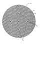
図6(断面側面図)および図7A(平面図)にも示したように、少なくとも1つのセンサ50が、基板ホルダ20に結合されている。例えば、少なくとも1つのセンサ50は、少なくとも1つのアンテナ電極52、少なくとも1つのアンテナリード線54および少なくとも1つの電気測定装置56を備えることができる。少なくとも1つのアンテナ電極52が、その上面近傍のセラミック層134内に埋設されており、その中から少なくとも1つのアンテナリード線54がクランプ電極132の開口部136を通って延長し、少なくとも1つの電極52に結合されている。少なくとも1つのアンテナ電極52に接続された少なくとも1つのアンテナリード線54が、さらに少なくとも1つの電気測定装置56に接続されている。少なくとも1つのセンサ50が、少なくとも1つの電気信号を測定し、次にこれをコントローラ55に供給する。別の実施形態において、図7Bに示したように、少なくとも1つのアンテナ電極52が楕円形状になっている。別の実施形態において、図7Cに示したように、少なくとも1つのアンテナ電極52が「腎臓形状」になっている。別の実施形態において、少なくとも1つの電極52を矩形状にすることもできる。別の実施形態において、図7Dに示したように、アンテナ電極52の配置を種々の位置に変えることもできる。しかし、アンテナの多数の配置およびアンテナの数は本発明に基づいて使用できることを理解しなければならない。 As shown in FIG. 6 (cross-sectional side view) and FIG. 7A (plan view), at least one
クランプ電極132を参照して、少なくとも1つのアンテナ電極52および少なくとも1つのアンテナリード線54の1つまたは複数の導電素子は、銅または同様の導電性物質から製造することができる。好ましい実施形態において、少なくとも1つのアンテナリード線54は外部導電性シールドを使用してシールドされ、またクランプ電極132およびRFバイアス可能電極126から絶縁されている。 With reference to the
図8Aは、静電クランプ装置130とRFバイアス可能電極126内に埋設された、アンテナ電極52とアンテナリード線54の分解組立図である。アンテナリード線54は、内部導電体素子542、内部誘電体素子544、外部導電体素子546および外部誘電体素子548を備えている。内部誘電体素子544は、内部導電体素子542を取り巻いていおり、また内部導電体素子542を外部導電体素子546から絶縁している。外部導電体素子546が内部誘電体素子544を取り巻いており、また内部導電体素子542をシールドしている。外部誘電体素子548は外部導電体素子546を取り巻いており、また外部導電体素子546をRFバイアス可能電極126から絶縁している。外部導電体素子546は電気的に接地されているのが望ましい。別の実施形態において、図8Bに示したように、アンテナ電極52の上面はセラミック層134の上面と同平面にない。 FIG. 8A is an exploded view of
静電クランプ装置130は、クランプ電極132、絶縁層134および少なくとも1つのアンテナリード線54を伴った、少なくとも1つの埋設アンテナ電極52を備えている。この種の静電クランプ装置130は、焼結技術、鋳造技術および/または薄膜形成技術(例えば、工業界では標準となっており、また現在静電チャック製造技術分野の当業者にとって周知である化学蒸着(CVD)のような)を使用して製造することができる。代表的な技術は、米国特許第5539179号、同第5625526号および同第5701228号(3つの特許は全て東京エレクトロン株式会社に譲渡されている)に開示されており、各々は参照して全体としてここに組み込まれる。 The
図6に示すように、少なくとも1つの電気測定装置56は少なくとも1つのアンテナリード線に接続され、例えばRF電圧測定を実行する。例えば、各電気測定装置56は、テクトロニクス株式会社(Tektronix)によって製造された(高インピーダンス)Tektronix P6245 1.5GHz 10X Active Probeとすることができる。少なくとも1つのセンサ50によって生成された信号は、例えばアナログ−デジタル(A/D)コンバータを使用する、例えばデジタル信号処理装置(DSP)のようなコントローラ55に入力することができる。 As shown in FIG. 6, at least one
図6および図8Aから8Dに示したアンテナ電極52およびアンテナリード線54は、静電クランプ装置130とRFバイアス可能電極126内に製造することができるが、アンテナ電極52およびアンテナリード線54は、例えばフォーカスリング128、誘電体リング124、外部シールド122、シールドリング、チャンバ壁、チャンバライナー等のような他の構造内に製造することもできる。例えば、図8Cと8Dは、RFバイアス可能電極126上に載置されたフォーカスリング560内に埋設された消耗可能電極570を表しており、この消耗可能電極570は凸面580を備え、この消耗可能電極570をアンテナ電極52と電気的に結合することができる。図8Cにおいて、消耗可能電極570はフォーカスリング560の上面と同平面をなし、また図8Dにおいて、消耗可能電極570はフォーカスリング560の上面と同平面をなしていない。従来のシステムにおいて、フォーカスリング560はRFバイアス可能電極126上反復可能交換用に設計されており、これによって消耗可能電極570はアンテナ電極52と絶えず結合することができる。フォーカスリング128または560は、例えばシリコン、シリコンカーバイド、アルミナまたは水晶の少なくとも1つを備えることができる。付加的に、消耗可能電極570は、例えばドープされたシリコン、またはタングステンのような埋設された導電性物質を備えることもできる。 The
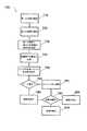
アーク抑制システムを使用する方法を次に説明する。図9は本発明の実施形態に基づくアーク抑制手順のためのフロー図を示す。手順600は、ステップ610で開始され、ここで少なくとも1つの信号が少なくとも1つのセンサを使用して測定される。例えば、少なくとも1つのセンサは、少なくとも1つの電気測定装置に接続された少なくとも1つのアンテナリード線に接続される、少なくとも1つのアンテナ電極を備えることができる。この信号は例えば、電圧プローブを使用して測定された時変電圧信号または時変電圧振幅である。別の実施形態において、センサによって測定された信号は、ローパス(低域)フィルタ、ハイパス(高域)フィルタ、および/またはバンドパス(帯域)フィルタを使用してフィルタすることができる。フィルタされた信号(被フィルタ信号)は、例えば被フィルタ時変電圧信号または被フィルタ時変電圧振幅となる。ステップ620において、測定信号および/または被フィルタ信号が基準信号と比較され、差信号が決定される。例えば、接地電位またはシステムの別の電位点が基準電位として使用することができる。差信号は、例えばある時刻の瞬時において測定された信号の瞬時値と接地電位または測定信号の振幅間の差、ある時刻の瞬時において測定されたフィルタ化信号の瞬時値と接地電位または被フィルタ信号の振幅間の差とすることができる。例えば、差信号は減算操作によって決定することができる。 A method of using the arc suppression system will now be described. FIG. 9 shows a flow diagram for an arc suppression procedure according to an embodiment of the present invention. The
ステップ630において、差信号が図10に示した目標差と比較される。図10は時刻に対する代表的な差信号634を目標差632(破線によって指示した)を重ねて示す。観察すると、測定差信号が目標差信号を超える時刻636が矢印で指示されている。ステップ640において、プラズマ処理システムの状態が、ステップ630における比較を使用して決定される。例えば、差信号が目標差を超えれば、アーク発生事象の確率が比較的高くなり、また少なくとも1つの差信号が目標差を超えなければ、アーク発生事象の確率が比較的低い。ステップ640における決定に基づいて、アーク警告の提示の決定がステップ650において実行される。例えば、アーク発生事象の確率が比較的高ければ、オペレータはステップ660において通知を受け、またアーク発生事象の確率が比較的低ければ、処理がステップ670において続行される。 In
さらに、アーク警告の事象において、処理がステップ660においてオペレータの次の通知によって調整することができる。ステップ680において、ステップ670において処理を続行するか、ステップ690において処理を中止するか、またステップ695において処理を修正するかを含む処理の調整が決定される。別の実施形態において、ステップ680における処理を制御する決定が、コントローラによってステップ660におけるオペレータの通知と同時に実行される。別の実施形態において、ステップ680における処理を制御する決定が、ステップ660におけるアーク発生事象の確率の単なるログ操作と同時に実行される。別の実施形態において、ステップ680における処理を制御する決定が、ステップ660におけるオペレータの通知なしに実行される。ステップ695において、処理が処理パラメータを調節することによって修正することができる。例えば、処理パラメータに、処理圧力、基板ホルダRFバイアス、静電クランプ電極バイアス、裏面ガス圧、処理ガス流量等を含ませることができる。 Further, in the event of an arc warning, the process can be adjusted at
図11は、本発明の別の実施形態に基づくアーク抑制手順のためのフロー図を示す。手順700はステップ710から開始され、ここでプラズマ処理システムに関連する第1の信号が第1のセンサを使用して測定される。例えば、第1のセンサは第1の電気測定装置に接続された第1のアンテナリード線に接続された第1のアンテナ電極を備えることができる。例えば、第1の信号は異質の第1の領域から導出される。例えば第1の信号は、例えば電圧プローブを使用して測定された時変電圧信号または時変電圧振幅とすることができる。別の実施形態において、第1のセンサによって測定された第1の信号は、ローパスフィルタ、ハイパスフィルタおよび/またはバンドパスフィルタを使用してフィルタすることができる。被フィルタ信号は、例えば被フィルタ時変電圧信号または被フィルタ時変電圧振幅とすることができる。 FIG. 11 shows a flow diagram for an arc suppression procedure according to another embodiment of the present invention.
ステップ720において、プラズマ処理システムに関連する第2の信号が第2のセンサを使用して測定される。例えば、第2のセンサは第2の電気測定装置に接続された第2のアンテナリード線に接続された第2のアンテナ電極を備えることができる。例えば、第2の信号は基板の第2の領域から導出される。例えば第2の信号は、例えば電圧プローブを使用して測定された時変電圧信号または時変電圧振幅とすることができる。別の実施形態において、第2の電気センサによって測定された第2の信号は、ローパスフィルタ、ハイパスフィルタおよび/またはバンドパスフィルタを使用してフィルタすることができる。被フィルタ信号は、例えば被フィルタ時変電圧信号または被フィルタ時変電圧振幅とすることができる。第1の信号および第2の信号の捕捉は、同時に実行されるのが好ましい。 In
一実施形態において、第1の信号は基板中心近傍のロケーション(位置)に対応し、また第2の信号は基板エッジ近傍のロケーションに対応する。別の実施形態において、第1の信号は基板エッジに対応し、また第2の信号がフォーカスリング近傍のロケーションに対応している。 In one embodiment, the first signal corresponds to a location near the substrate center and the second signal corresponds to a location near the substrate edge. In another embodiment, the first signal corresponds to a substrate edge and the second signal corresponds to a location near the focus ring.
別の実施形態において、第1の信号は第1のロケーションと第1の測定時刻に対応し、また第2の信号が第1のロケーションと第2の測定時刻に対応している。同じロケーションであるが異なる時刻における第1の信号と第2の信号の測定は、測定の変化量の検査を可能にする。 In another embodiment, the first signal corresponds to a first location and a first measurement time, and the second signal corresponds to a first location and a second measurement time. Measurement of the first signal and the second signal at the same location but at different times allows examination of the measurement variation.
ステップ730において、差信号は、各瞬時における第1の信号と第2の信号の比較によって決定される。例えば、差信号は第1の信号の瞬時値と第2の信号の瞬時値間の差、第1の信号の振幅と第2の信号の振幅間の差、被フィルタ第1の信号の瞬時値と被フィルタ第2の信号の瞬時値間の差、または被フィルタ第1の信号の振幅と被フィルタ第2の信号の振幅間の差とすることができる。 In
ステップ740において、差信号が図10に示したように目標差と比較される。図10は時刻に対する代表的な差信号634を目標差632(破線によって指示した)を重ねて示す。観察すると、測定差信号が目標差信号を超える時刻636が矢印で指示されている。ステップ750において、プラズマ処理システムの状態が、ステップ740における比較を使用して決定される。例えば、差信号が目標差を超えれば、アーク発生事象の確率が比較的高くなり、また少なくとも1つの差信号が目標差を超えなければ、アーク発生事象の確率が比較的低い。ステップ750における決定に基づいて、アーク警告の提示の決定がステップ760において実行される。例えば、アーク発生事象の確率が比較的高ければ、オペレータはステップ770において通知を受け、またアーク発生事象の確率が比較的低ければ、処理がステップ780において続行される。 In
2つ以上の信号が利用されたときに、付加情報が提示される。例えば、アーク発生の最も高い確率に対するロケーションは、差信号の大きさが最高になるこれらの領域をモニタすることによって決定することができる。 Additional information is presented when more than one signal is used. For example, the location for the highest probability of arcing can be determined by monitoring those areas where the magnitude of the difference signal is highest.
さらに、アーク警告の事象において、処理がステップ770においてオペレータの次の通知によって制御されることができる。ステップ790において、ステップ780において処理を続行するか、ステップ800において処理を中止するか、またステップ810において処理を修正するかを含む処理の制御が決定される。別の実施形態において、ステップ790における処理を調整する決定が、コントローラによってステップ770におけるオペレータの通知と同時に実行される。別の実施形態において、ステップ790における処理を調整する決定が、ステップ770におけるアーク発生事象の確率の単なるログ操作と同時に実行される。別の実施形態において、ステップ790における処理を制御する決定が、ステップ770におけるオペレータの通知なしに実行される。ステップ810において、処理パラメータを調節することによって処理を修正することができる。例えば、処理パラメータに、処理圧力、基板ホルダRFバイアス、静電クランプ電極バイアス、裏面ガス圧、処理ガス流量等を含ませることができる。 Further, in the event of an arc warning, the process can be controlled at
本発明の特定の代表的実施形態のみをこれまでに詳述したが、多数の修正例も本発明の新規な教示および利点から実質的に逸脱することなく可能であることは、当業者にとって容易に理解できよう。従って、このような全ての修正例は本発明の範囲内に含まれることを意図している。 While only certain representative embodiments of the present invention have been described in detail above, it will be readily apparent to those skilled in the art that numerous modifications are possible without substantially departing from the novel teachings and advantages of the present invention. To understand. Accordingly, all such modifications are intended to be included within the scope of this invention.
Claims (64)
Translated fromJapanese前記処理反応装置に結合され、前記プラズマに関連する少なくとも1つの信号を発生するように構成された少なくとも1つのセンサと、前記少なくとも1つのセンサに結合されたコントローラとを備えるアーク抑制システムと、を具備するプラズマ処理システムであって、
前記コントローラは、前記少なくとも1つの信号を使用して前記プラズマ処理システムの状態を決定することと、前記状態により前記プラズマ処理システムを制御してアーク発生事象を抑制することとのうち少なくとも1つを実行させるように構成されるプラズマ処理システム。A processing reactor configured to facilitate the formation of plasma;
An arc suppression system comprising: at least one sensor coupled to the process reactor and configured to generate at least one signal associated with the plasma; and a controller coupled to the at least one sensor. A plasma processing system comprising:
The controller determines at least one of the state of the plasma processing system using the at least one signal and controls the plasma processing system according to the state to suppress an arcing event. A plasma processing system configured to be executed.
前記プラズマ処理システムに関連する前記少なくとも1つの信号を使用して前記プラズマ処理システムの状態を決定すること、およびアーク発生事象を抑制するために前記プラズマ処理システムの前記状態により前記プラズマ処理システムを制御することの少なくとも1つを実行させる少なくとも1つのアルゴリズムを実行するように構成されたコントローラと、
を具備するアーク抑制システム。At least one sensor configured to be coupled to the plasma processing system;
Determining the state of the plasma processing system using the at least one signal associated with the plasma processing system and controlling the plasma processing system according to the state of the plasma processing system to suppress arcing events; A controller configured to execute at least one algorithm that causes at least one of performing
An arc suppression system comprising:
前記少なくとも1つのセンサを使用して、前記プラズマ処理システムに関連する少なくとも1つの信号を測定することと、
前記少なくとも1つの信号と基準信号間の少なくとも1つの差信号を決定することと、
前記少なくとも1つの差信号を目標差と比較することと、
前記比較から前記プラズマ処理システムの状態を決定することと、を具備し、
前記少なくとも1つの信号は、基板ホルダ、チャンバ壁およびチャンバライナーの少なくとも1つの中に埋設された少なくとも1つのアンテナを備える、少なくとも1つのセンサを使用して測定される方法。A method for suppressing arc generation in the plasma processing system using an arc suppression system comprising at least one sensor coupled to the plasma processing system and a controller coupled to the at least one sensor. ,
Measuring at least one signal associated with the plasma processing system using the at least one sensor;
Determining at least one difference signal between the at least one signal and a reference signal;
Comparing the at least one difference signal with a target difference;
Determining a state of the plasma processing system from the comparison; and
The method wherein the at least one signal is measured using at least one sensor comprising at least one antenna embedded in at least one of a substrate holder, a chamber wall and a chamber liner.
第1のセンサを使用して前記プラズマ処理システムに関連する第1の信号を測定することと、
第2のセンサを使用して前記プラズマ処理システムに関連する第2の信号を測定することと、
前記第1の信号と前記第2の信号間の差信号を決定することと、
前記差信号を目標差と比較することと、
前記比較により前記プラズマ処理システムの状態を決定することとを具備する方法。A method for suppressing arc generation in the plasma processing system using an arc suppression system comprising at least one sensor coupled to the plasma processing system and a controller coupled to the at least one sensor comprising:
Measuring a first signal associated with the plasma processing system using a first sensor;
Measuring a second signal associated with the plasma processing system using a second sensor;
Determining a difference signal between the first signal and the second signal;
Comparing the difference signal with a target difference;
Determining the state of the plasma processing system by the comparison.
前記プラズマ反応装置に結合され、前記プラズマに関連する少なくとも1つの信号を発生する手段を備えるアーク抑制手段と、
前記少なくとも1つのセンサに結合され、前記少なくとも1つの信号を使用して前記プラズマ処理システムの状態を決定することと、アーク発生事象を抑制する前記状態により前記プラズマ処理システムを制御することとのうち少なくとも1つを実行する制御手段とを具備するプラズマ処理システム。A plasma reactor configured to facilitate plasma formation;
Arc suppression means coupled to the plasma reactor and comprising means for generating at least one signal associated with the plasma;
Coupling the at least one sensor and using the at least one signal to determine a state of the plasma processing system and controlling the plasma processing system with the state to suppress an arcing event. A plasma processing system comprising control means for executing at least one.
Applications Claiming Priority (2)
| Application Number | Priority Date | Filing Date | Title |
|---|---|---|---|
| US39195002P | 2002-06-28 | 2002-06-28 | |
| PCT/US2003/016243WO2004003968A2 (en) | 2002-06-28 | 2003-06-27 | Method and system for arc suppression in a plasma processing system |
Publications (1)
| Publication Number | Publication Date |
|---|---|
| JP2006507662Atrue JP2006507662A (en) | 2006-03-02 |
Family
ID=30000781
Family Applications (1)
| Application Number | Title | Priority Date | Filing Date |
|---|---|---|---|
| JP2004517580APendingJP2006507662A (en) | 2002-06-28 | 2003-06-27 | Arc suppression method and system in plasma processing system |
Country Status (5)
| Country | Link |
|---|---|
| US (1) | US7199327B2 (en) |
| JP (1) | JP2006507662A (en) |
| CN (1) | CN100360704C (en) |
| AU (1) | AU2003280398A1 (en) |
| WO (1) | WO2004003968A2 (en) |
Cited By (6)
| Publication number | Priority date | Publication date | Assignee | Title |
|---|---|---|---|---|
| WO2012039867A1 (en)* | 2010-09-23 | 2012-03-29 | Applied Materials, Inc. | System and method for voltage-based plasma excursion detection |
| WO2012039885A3 (en)* | 2010-09-24 | 2012-05-31 | Applied Materials, Inc. | System and method for current-based plasma excursion detection |
| JP2012116749A (en)* | 2007-04-27 | 2012-06-21 | Applied Materials Inc | Apparatus and method for reducing erosion rate of surface exposed to halogen-containing plasma |
| JP2019096650A (en)* | 2017-11-17 | 2019-06-20 | 東京エレクトロン株式会社 | Plasma processing apparatus |
| KR20210065217A (en)* | 2019-11-26 | 2021-06-04 | (주)제니스월드 | Wireless charging electrostatic chuck and substrate processing system using the same |
| KR102274530B1 (en)* | 2021-01-11 | 2021-07-07 | 티오에스주식회사 | Device for detecting plasma of ultra fast with multi channel |
Families Citing this family (59)
| Publication number | Priority date | Publication date | Assignee | Title |
|---|---|---|---|---|
| US7960670B2 (en)* | 2005-05-03 | 2011-06-14 | Kla-Tencor Corporation | Methods of and apparatuses for measuring electrical parameters of a plasma process |
| US20080264564A1 (en) | 2007-04-27 | 2008-10-30 | Applied Materials, Inc. | Method of reducing the erosion rate of semiconductor processing apparatus exposed to halogen-containing plasmas |
| US7988833B2 (en) | 2002-04-12 | 2011-08-02 | Schneider Electric USA, Inc. | System and method for detecting non-cathode arcing in a plasma generation apparatus |
| US7981257B2 (en) | 2002-04-12 | 2011-07-19 | Schneider Electric USA, Inc. | Current-based method and apparatus for detecting and classifying arcs |
| JP3748559B2 (en)* | 2003-06-30 | 2006-02-22 | キヤノン株式会社 | Stage apparatus, exposure apparatus, charged beam drawing apparatus, device manufacturing method, substrate potential measuring method, and electrostatic chuck |
| EP1675155B1 (en)* | 2004-12-24 | 2012-01-25 | HÜTTINGER Elektronik GmbH + Co. KG | Plasma excitation system |
| US7305311B2 (en)* | 2005-04-22 | 2007-12-04 | Advanced Energy Industries, Inc. | Arc detection and handling in radio frequency power applications |
| US20070042131A1 (en)* | 2005-08-22 | 2007-02-22 | Applied Materials, Inc., A Delaware Corporation | Non-intrusive plasma monitoring system for arc detection and prevention for blanket CVD films |
| TW200835923A (en)* | 2006-09-15 | 2008-09-01 | Schneider Automation | System and method for detecting non-cathode arcing in a plasma generation apparatus |
| PL2158977T3 (en)* | 2006-10-27 | 2017-10-31 | Oerlikon Surface Solutions Ag Pfaeffikon | Method and apparatus for manufacturing cleaned substrates or clean substrates which are further processed |
| US7795817B2 (en)* | 2006-11-24 | 2010-09-14 | Huettinger Elektronik Gmbh + Co. Kg | Controlled plasma power supply |
| US8941037B2 (en)* | 2006-12-25 | 2015-01-27 | Tokyo Electron Limited | Substrate processing apparatus, focus ring heating method, and substrate processing method |
| US10242888B2 (en) | 2007-04-27 | 2019-03-26 | Applied Materials, Inc. | Semiconductor processing apparatus with a ceramic-comprising surface which exhibits fracture toughness and halogen plasma resistance |
| US10622194B2 (en) | 2007-04-27 | 2020-04-14 | Applied Materials, Inc. | Bulk sintered solid solution ceramic which exhibits fracture toughness and halogen plasma resistance |
| US7737702B2 (en)* | 2007-08-15 | 2010-06-15 | Applied Materials, Inc. | Apparatus for wafer level arc detection at an electrostatic chuck electrode |
| US7733095B2 (en)* | 2007-08-15 | 2010-06-08 | Applied Materials, Inc. | Apparatus for wafer level arc detection at an RF bias impedance match to the pedestal electrode |
| US7750645B2 (en)* | 2007-08-15 | 2010-07-06 | Applied Materials, Inc. | Method of wafer level transient sensing, threshold comparison and arc flag generation/deactivation |
| US7768269B2 (en)* | 2007-08-15 | 2010-08-03 | Applied Materials, Inc. | Method of multi-location ARC sensing with adaptive threshold comparison |
| US7750644B2 (en)* | 2007-08-15 | 2010-07-06 | Applied Materials, Inc. | System with multi-location arc threshold comparators and communication channels for carrying arc detection flags and threshold updating |
| WO2009076568A2 (en)* | 2007-12-13 | 2009-06-18 | Lam Research Corporation | Plasma unconfinement sensor and methods thereof |
| US8264237B2 (en)* | 2008-02-14 | 2012-09-11 | Mks Instruments, Inc. | Application of wideband sampling for arc detection with a probabilistic model for quantitatively measuring arc events |
| US8334700B2 (en)* | 2008-02-14 | 2012-12-18 | Mks Instruments, Inc. | Arc detection |
| US8289029B2 (en)* | 2008-02-14 | 2012-10-16 | Mks Instruments, Inc. | Application of wideband sampling for arc detection with a probabilistic model for quantitatively measuring arc events |
| KR101111494B1 (en)* | 2008-02-18 | 2012-02-23 | 미쯔이 죠센 가부시키가이샤 | Atomic deposition apparatus and atomic layer deposition method |
| US8022718B2 (en)* | 2008-02-29 | 2011-09-20 | Lam Research Corporation | Method for inspecting electrostatic chucks with Kelvin probe analysis |
| US8158017B2 (en)* | 2008-05-12 | 2012-04-17 | Lam Research Corporation | Detection of arcing events in wafer plasma processing through monitoring of trace gas concentrations |
| JP5012701B2 (en)* | 2008-07-02 | 2012-08-29 | パナソニック株式会社 | Plasma processing apparatus and discharge state monitoring method in plasma processing apparatus |
| TWI511622B (en)* | 2008-07-07 | 2015-12-01 | Lam Res Corp | Passive capacitively-coupled electrostatic(cce) probe arrangement for detecting in-situ arcing events in a plasma processing chamber |
| KR101799603B1 (en)* | 2009-06-30 | 2017-11-20 | 램 리써치 코포레이션 | Automatic fault detection and classification in a plasma processing system and methods thereof |
| US8501631B2 (en)* | 2009-11-19 | 2013-08-06 | Lam Research Corporation | Plasma processing system control based on RF voltage |
| US9083182B2 (en) | 2011-11-21 | 2015-07-14 | Lam Research Corporation | Bypass capacitors for high voltage bias power in the mid frequency RF range |
| US9263240B2 (en) | 2011-11-22 | 2016-02-16 | Lam Research Corporation | Dual zone temperature control of upper electrodes |
| US10586686B2 (en) | 2011-11-22 | 2020-03-10 | Law Research Corporation | Peripheral RF feed and symmetric RF return for symmetric RF delivery |
| US9396908B2 (en) | 2011-11-22 | 2016-07-19 | Lam Research Corporation | Systems and methods for controlling a plasma edge region |
| KR101971312B1 (en)* | 2011-11-23 | 2019-04-22 | 램 리써치 코포레이션 | Multi zone gas injection upper electrode system |
| WO2013078434A1 (en) | 2011-11-24 | 2013-05-30 | Lam Research Corporation | Plasma processing chamber with flexible symmetric rf return strap |
| US9320126B2 (en) | 2012-12-17 | 2016-04-19 | Lam Research Corporation | Determining a value of a variable on an RF transmission model |
| US10157729B2 (en) | 2012-02-22 | 2018-12-18 | Lam Research Corporation | Soft pulsing |
| US9462672B2 (en) | 2012-02-22 | 2016-10-04 | Lam Research Corporation | Adjustment of power and frequency based on three or more states |
| US9842725B2 (en) | 2013-01-31 | 2017-12-12 | Lam Research Corporation | Using modeling to determine ion energy associated with a plasma system |
| US9197196B2 (en) | 2012-02-22 | 2015-11-24 | Lam Research Corporation | State-based adjustment of power and frequency |
| US9114666B2 (en) | 2012-02-22 | 2015-08-25 | Lam Research Corporation | Methods and apparatus for controlling plasma in a plasma processing system |
| US10128090B2 (en) | 2012-02-22 | 2018-11-13 | Lam Research Corporation | RF impedance model based fault detection |
| US9673069B2 (en)* | 2012-07-20 | 2017-06-06 | Applied Materials, Inc. | High frequency filter for improved RF bias signal stability |
| CN104730372B (en)* | 2013-12-13 | 2018-08-10 | 朗姆研究公司 | Fault detect based on RF impedance models |
| US9594105B2 (en) | 2014-01-10 | 2017-03-14 | Lam Research Corporation | Cable power loss determination for virtual metrology |
| US10950421B2 (en) | 2014-04-21 | 2021-03-16 | Lam Research Corporation | Using modeling for identifying a location of a fault in an RF transmission system for a plasma system |
| US10522330B2 (en) | 2015-06-12 | 2019-12-31 | Varian Semiconductor Equipment Associates, Inc. | In-situ plasma cleaning of process chamber components |
| US20170092473A1 (en)* | 2015-09-28 | 2017-03-30 | Varian Semiconductor Equipment Associates, Inc. | In-situ plasma cleaning of process chamber electrostatic elements having varied geometries |
| GB201615114D0 (en)* | 2016-09-06 | 2016-10-19 | Spts Technologies Ltd | A Method and system of monitoring and controlling deformation of a wafer substrate |
| US20200048770A1 (en)* | 2018-08-07 | 2020-02-13 | Lam Research Corporation | Chemical vapor deposition tool for preventing or suppressing arcing |
| CN109854483B (en)* | 2019-02-22 | 2020-05-05 | 深圳市圆梦精密技术研究院 | Vacuum device |
| US11521832B2 (en)* | 2020-01-10 | 2022-12-06 | COMET Technologies USA, Inc. | Uniformity control for radio frequency plasma processing systems |
| CN114695044A (en)* | 2020-12-29 | 2022-07-01 | 中微半导体设备(上海)股份有限公司 | Base assembly and plasma processing equipment |
| KR20230006725A (en)* | 2021-07-02 | 2023-01-11 | 삼성전자주식회사 | System of semiconductor process and control method thereof |
| KR20230036847A (en) | 2021-09-08 | 2023-03-15 | 삼성전자주식회사 | High voltage power supplying apparatus and plasma etching equipment having the same |
| US20230170192A1 (en)* | 2021-11-29 | 2023-06-01 | Applied Materials, Inc. | Method and apparatus for realtime wafer potential measurement in a plasma processing chamber |
| US12434341B2 (en)* | 2022-04-22 | 2025-10-07 | Samsung Electronics Co., Ltd. | Electrostatic chuck apparatus |
| US12176190B2 (en)* | 2023-03-07 | 2024-12-24 | Applied Materials, Inc. | Arc management algorithm of RF generator and match box for CCP plasma chambers |
Citations (5)
| Publication number | Priority date | Publication date | Assignee | Title |
|---|---|---|---|---|
| JPH07169702A (en)* | 1993-12-13 | 1995-07-04 | Kokusai Electric Co Ltd | Temperature detector for semiconductor manufacturing equipment |
| JPH08335567A (en)* | 1995-06-07 | 1996-12-17 | Tokyo Electron Ltd | Plasma treatment apparatus |
| JP2000269108A (en)* | 1999-03-15 | 2000-09-29 | Sharp Corp | Management system for semiconductor manufacturing equipment |
| JP2001148374A (en)* | 1999-07-27 | 2001-05-29 | Applied Materials Inc | Capacitive probe for in situ measurement of wafer DC bias voltage |
| JP2001516940A (en)* | 1997-09-17 | 2001-10-02 | 東京エレクトロン株式会社 | Apparatus and method for detecting and preventing arcing in RF plasma systems |
Family Cites Families (7)
| Publication number | Priority date | Publication date | Assignee | Title |
|---|---|---|---|---|
| US5241152A (en)* | 1990-03-23 | 1993-08-31 | Anderson Glen L | Circuit for detecting and diverting an electrical arc in a glow discharge apparatus |
| DE4127504A1 (en)* | 1991-08-20 | 1993-02-25 | Leybold Ag | DEVICE FOR SUPPRESSING ARCES |
| DE4202425C2 (en)* | 1992-01-29 | 1997-07-17 | Leybold Ag | Method and device for coating a substrate, in particular with electrically non-conductive layers |
| DE4441206C2 (en) | 1994-11-19 | 1996-09-26 | Leybold Ag | Device for the suppression of rollovers in cathode sputtering devices |
| US5584972A (en)* | 1995-02-01 | 1996-12-17 | Sony Corporation | Plasma noise and arcing suppressor apparatus and method for sputter deposition |
| US5993615A (en)* | 1997-06-19 | 1999-11-30 | International Business Machines Corporation | Method and apparatus for detecting arcs |
| US6318384B1 (en)* | 1999-09-24 | 2001-11-20 | Applied Materials, Inc. | Self cleaning method of forming deep trenches in silicon substrates |
- 2003
- 2003-06-27JPJP2004517580Apatent/JP2006507662A/enactivePending
- 2003-06-27AUAU2003280398Apatent/AU2003280398A1/ennot_activeAbandoned
- 2003-06-27USUS10/512,862patent/US7199327B2/ennot_activeExpired - Lifetime
- 2003-06-27CNCNB038152754Apatent/CN100360704C/ennot_activeExpired - Fee Related
- 2003-06-27WOPCT/US2003/016243patent/WO2004003968A2/enactiveSearch and Examination
Patent Citations (5)
| Publication number | Priority date | Publication date | Assignee | Title |
|---|---|---|---|---|
| JPH07169702A (en)* | 1993-12-13 | 1995-07-04 | Kokusai Electric Co Ltd | Temperature detector for semiconductor manufacturing equipment |
| JPH08335567A (en)* | 1995-06-07 | 1996-12-17 | Tokyo Electron Ltd | Plasma treatment apparatus |
| JP2001516940A (en)* | 1997-09-17 | 2001-10-02 | 東京エレクトロン株式会社 | Apparatus and method for detecting and preventing arcing in RF plasma systems |
| JP2000269108A (en)* | 1999-03-15 | 2000-09-29 | Sharp Corp | Management system for semiconductor manufacturing equipment |
| JP2001148374A (en)* | 1999-07-27 | 2001-05-29 | Applied Materials Inc | Capacitive probe for in situ measurement of wafer DC bias voltage |
Cited By (10)
| Publication number | Priority date | Publication date | Assignee | Title |
|---|---|---|---|---|
| JP2012116749A (en)* | 2007-04-27 | 2012-06-21 | Applied Materials Inc | Apparatus and method for reducing erosion rate of surface exposed to halogen-containing plasma |
| WO2012039867A1 (en)* | 2010-09-23 | 2012-03-29 | Applied Materials, Inc. | System and method for voltage-based plasma excursion detection |
| US8502689B2 (en) | 2010-09-23 | 2013-08-06 | Applied Materials, Inc. | System and method for voltage-based plasma excursion detection |
| TWI452600B (en)* | 2010-09-23 | 2014-09-11 | Applied Materials Inc | System and method for voltage-based plasma excursion detection |
| WO2012039885A3 (en)* | 2010-09-24 | 2012-05-31 | Applied Materials, Inc. | System and method for current-based plasma excursion detection |
| US8587321B2 (en) | 2010-09-24 | 2013-11-19 | Applied Materials, Inc. | System and method for current-based plasma excursion detection |
| JP2019096650A (en)* | 2017-11-17 | 2019-06-20 | 東京エレクトロン株式会社 | Plasma processing apparatus |
| KR20210065217A (en)* | 2019-11-26 | 2021-06-04 | (주)제니스월드 | Wireless charging electrostatic chuck and substrate processing system using the same |
| KR102352650B1 (en)* | 2019-11-26 | 2022-01-20 | (주)제니스월드 | Wireless charging electrostatic chuck and substrate processing system using the same |
| KR102274530B1 (en)* | 2021-01-11 | 2021-07-07 | 티오에스주식회사 | Device for detecting plasma of ultra fast with multi channel |
Also Published As
| Publication number | Publication date |
|---|---|
| CN100360704C (en) | 2008-01-09 |
| WO2004003968A2 (en) | 2004-01-08 |
| AU2003280398A1 (en) | 2004-01-19 |
| WO2004003968A3 (en) | 2004-09-10 |
| US7199327B2 (en) | 2007-04-03 |
| CN1665955A (en) | 2005-09-07 |
| AU2003280398A8 (en) | 2004-01-19 |
| US20060081564A1 (en) | 2006-04-20 |
Similar Documents
| Publication | Publication Date | Title |
|---|---|---|
| US7199327B2 (en) | Method and system for arc suppression in a plasma processing system | |
| US10090160B2 (en) | Dry etching apparatus and method | |
| US7658816B2 (en) | Focus ring and plasma processing apparatus | |
| CN109216144B (en) | Plasma reactor with low-frequency radio frequency power distribution adjusting function | |
| US6214162B1 (en) | Plasma processing apparatus | |
| JP5454467B2 (en) | Plasma etching processing apparatus and plasma etching processing method | |
| EP1840937B1 (en) | Plasma processing apparatus and plasma processing method | |
| JP6442463B2 (en) | Annular baffle | |
| TW201931428A (en) | Plasma reactor having a function of tuning low frequency RF power distribution | |
| US20040040931A1 (en) | Plasma processing method and plasma processor | |
| JP3150058B2 (en) | Plasma processing apparatus and plasma processing method | |
| CN101506950A (en) | Hybrid RF capacitively and inductively coupled plasma source using multi-frequency RF power and method of using the same | |
| KR20010087195A (en) | Plasma processing apparatus and plasma processing method | |
| KR100842947B1 (en) | Plasma processing method and plasma processing apparatus | |
| TW202329193A (en) | Distortion current mitigation in a radio frequency plasma processing chamber | |
| US20060021580A1 (en) | Plasma processing apparatus and impedance adjustment method | |
| US20070256638A1 (en) | Electrode plate for use in plasma processing and plasma processing system | |
| CN115398602B (en) | Plasma processing apparatus and plasma processing method | |
| KR20060056972A (en) | How to balance regression currents in plasma processing equipment | |
| JP2003224112A (en) | Plasma treatment device and plasma treatment method | |
| KR102498944B1 (en) | Process for performing self-limited etching of organic materials | |
| JP3372244B2 (en) | Plasma processing equipment | |
| JP4388455B2 (en) | Plasma etching processing equipment | |
| US20240194446A1 (en) | Chamber impedance management in a processing chamber | |
| JPH06120140A (en) | Semiconductor manufacturing method and device |
Legal Events
| Date | Code | Title | Description |
|---|---|---|---|
| A131 | Notification of reasons for refusal | Free format text:JAPANESE INTERMEDIATE CODE: A131 Effective date:20080603 | |
| A521 | Request for written amendment filed | Free format text:JAPANESE INTERMEDIATE CODE: A523 Effective date:20080804 | |
| A02 | Decision of refusal | Free format text:JAPANESE INTERMEDIATE CODE: A02 Effective date:20081111 | |
| A521 | Request for written amendment filed | Free format text:JAPANESE INTERMEDIATE CODE: A523 Effective date:20090113 | |
| A911 | Transfer to examiner for re-examination before appeal (zenchi) | Free format text:JAPANESE INTERMEDIATE CODE: A911 Effective date:20090302 | |
| A912 | Re-examination (zenchi) completed and case transferred to appeal board | Free format text:JAPANESE INTERMEDIATE CODE: A912 Effective date:20090710 |