JP2006506811A - Method and apparatus for providing a universal metal delivery source (GMDS) and integrating the universal metal delivery source with atomic layer deposition (ALD) - Google Patents
Method and apparatus for providing a universal metal delivery source (GMDS) and integrating the universal metal delivery source with atomic layer deposition (ALD)Download PDFInfo
- Publication number
- JP2006506811A JP2006506811AJP2004551983AJP2004551983AJP2006506811AJP 2006506811 AJP2006506811 AJP 2006506811AJP 2004551983 AJP2004551983 AJP 2004551983AJP 2004551983 AJP2004551983 AJP 2004551983AJP 2006506811 AJP2006506811 AJP 2006506811A
- Authority
- JP
- Japan
- Prior art keywords
- gas
- source
- reaction chamber
- metal
- volatile
- Prior art date
- Legal status (The legal status is an assumption and is not a legal conclusion. Google has not performed a legal analysis and makes no representation as to the accuracy of the status listed.)
- Pending
Links
- 229910052751metalInorganic materials0.000claimsabstractdescription92
- 239000002184metalSubstances0.000claimsabstractdescription91
- 238000006243chemical reactionMethods0.000claimsabstractdescription78
- 239000007787solidSubstances0.000claimsabstractdescription58
- 239000000463materialSubstances0.000claimsabstractdescription45
- 150000002736metal compoundsChemical class0.000claimsabstractdescription42
- 238000012545processingMethods0.000claimsabstractdescription22
- 238000010438heat treatmentMethods0.000claimsabstractdescription10
- 238000000231atomic layer depositionMethods0.000claimsdescription59
- 238000000034methodMethods0.000claimsdescription52
- 239000002243precursorSubstances0.000claimsdescription49
- 238000005229chemical vapour depositionMethods0.000claimsdescription40
- 230000008569processEffects0.000claimsdescription33
- 239000000460chlorineSubstances0.000claimsdescription21
- 239000000758substrateSubstances0.000claimsdescription15
- 229910052801chlorineInorganic materials0.000claimsdescription14
- ZAMOUSCENKQFHK-UHFFFAOYSA-NChlorine atomChemical compound[Cl]ZAMOUSCENKQFHK-UHFFFAOYSA-N0.000claimsdescription13
- 239000002994raw materialSubstances0.000claimsdescription13
- 239000011248coating agentSubstances0.000claimsdescription12
- 238000000576coating methodMethods0.000claimsdescription12
- 229910052715tantalumInorganic materials0.000claimsdescription12
- 238000000151depositionMethods0.000claimsdescription10
- 230000008021depositionEffects0.000claimsdescription10
- 238000010494dissociation reactionMethods0.000claimsdescription10
- 230000005593dissociationsEffects0.000claimsdescription10
- GUVRBAGPIYLISA-UHFFFAOYSA-Ntantalum atomChemical compound[Ta]GUVRBAGPIYLISA-UHFFFAOYSA-N0.000claimsdescription10
- 239000010453quartzSubstances0.000claimsdescription8
- VYPSYNLAJGMNEJ-UHFFFAOYSA-Nsilicon dioxideInorganic materialsO=[Si]=OVYPSYNLAJGMNEJ-UHFFFAOYSA-N0.000claimsdescription8
- 239000007769metal materialSubstances0.000claims2
- 229940126062Compound ADrugs0.000abstract1
- NLDMNSXOCDLTTB-UHFFFAOYSA-NHeterophylliin ANatural productsO1C2COC(=O)C3=CC(O)=C(O)C(O)=C3C3=C(O)C(O)=C(O)C=C3C(=O)OC2C(OC(=O)C=2C=C(O)C(O)=C(O)C=2)C(O)C1OC(=O)C1=CC(O)=C(O)C(O)=C1NLDMNSXOCDLTTB-UHFFFAOYSA-N0.000abstract1
- 239000007789gasSubstances0.000description67
- 239000010408filmSubstances0.000description20
- 239000010410layerSubstances0.000description10
- 238000004519manufacturing processMethods0.000description9
- XKRFYHLGVUSROY-UHFFFAOYSA-NArgonChemical compound[Ar]XKRFYHLGVUSROY-UHFFFAOYSA-N0.000description8
- 125000001309chloro groupChemical groupCl*0.000description8
- 230000015572biosynthetic processEffects0.000description7
- 238000013461designMethods0.000description7
- 229910052756noble gasInorganic materials0.000description7
- 239000010409thin filmSubstances0.000description7
- 238000011144upstream manufacturingMethods0.000description7
- 230000004907fluxEffects0.000description6
- 239000007788liquidSubstances0.000description6
- 229910052786argonInorganic materials0.000description5
- 238000011109contaminationMethods0.000description5
- 239000011261inert gasSubstances0.000description5
- 238000012423maintenanceMethods0.000description5
- IJGRMHOSHXDMSA-UHFFFAOYSA-NAtomic nitrogenChemical compoundN#NIJGRMHOSHXDMSA-UHFFFAOYSA-N0.000description4
- 238000010586diagramMethods0.000description4
- 238000005516engineering processMethods0.000description4
- 229910001507metal halideInorganic materials0.000description4
- 150000005309metal halidesChemical class0.000description4
- 239000000047productSubstances0.000description4
- 239000000126substanceSubstances0.000description4
- 235000012431wafersNutrition0.000description4
- PXHVJJICTQNCMI-UHFFFAOYSA-NNickelChemical compound[Ni]PXHVJJICTQNCMI-UHFFFAOYSA-N0.000description3
- 125000004429atomChemical group0.000description3
- 150000001875compoundsChemical class0.000description3
- 239000000356contaminantSubstances0.000description3
- 238000005530etchingMethods0.000description3
- 230000006872improvementEffects0.000description3
- 239000000203mixtureSubstances0.000description3
- 239000002245particleSubstances0.000description3
- 239000000376reactantSubstances0.000description3
- 239000004065semiconductorSubstances0.000description3
- 239000011343solid materialSubstances0.000description3
- WKBOTKDWSSQWDR-UHFFFAOYSA-NBromine atomChemical compound[Br]WKBOTKDWSSQWDR-UHFFFAOYSA-N0.000description2
- PXGOKWXKJXAPGV-UHFFFAOYSA-NFluorineChemical compoundFFPXGOKWXKJXAPGV-UHFFFAOYSA-N0.000description2
- 230000004075alterationEffects0.000description2
- 238000003877atomic layer epitaxyMethods0.000description2
- 230000008901benefitEffects0.000description2
- GDTBXPJZTBHREO-UHFFFAOYSA-NbromineSubstancesBrBrGDTBXPJZTBHREO-UHFFFAOYSA-N0.000description2
- 229910052794bromiumInorganic materials0.000description2
- 239000012159carrier gasSubstances0.000description2
- 239000007795chemical reaction productSubstances0.000description2
- 238000004140cleaningMethods0.000description2
- 239000013078crystalSubstances0.000description2
- 229910052731fluorineInorganic materials0.000description2
- 239000011737fluorineSubstances0.000description2
- 230000006870functionEffects0.000description2
- 238000010574gas phase reactionMethods0.000description2
- 229910044991metal oxideInorganic materials0.000description2
- 150000004706metal oxidesChemical class0.000description2
- 150000002739metalsChemical class0.000description2
- 229910052759nickelInorganic materials0.000description2
- 229910052757nitrogenInorganic materials0.000description2
- 238000005240physical vapour depositionMethods0.000description2
- 239000012713reactive precursorSubstances0.000description2
- 230000009257reactivityEffects0.000description2
- 238000011160researchMethods0.000description2
- 238000012827research and developmentMethods0.000description2
- 229910052710siliconInorganic materials0.000description2
- 229910052712strontiumInorganic materials0.000description2
- OKTJSMMVPCPJKN-UHFFFAOYSA-NCarbonChemical compound[C]OKTJSMMVPCPJKN-UHFFFAOYSA-N0.000description1
- XUIMIQQOPSSXEZ-UHFFFAOYSA-NSiliconChemical compound[Si]XUIMIQQOPSSXEZ-UHFFFAOYSA-N0.000description1
- 230000009471actionEffects0.000description1
- 230000002411adverseEffects0.000description1
- 229910052785arsenicInorganic materials0.000description1
- QVGXLLKOCUKJST-UHFFFAOYSA-Natomic oxygenChemical compound[O]QVGXLLKOCUKJST-UHFFFAOYSA-N0.000description1
- 229910052788bariumInorganic materials0.000description1
- 230000004888barrier functionEffects0.000description1
- 239000003990capacitorSubstances0.000description1
- 229910052799carbonInorganic materials0.000description1
- 239000013626chemical specieSubstances0.000description1
- 229910052804chromiumInorganic materials0.000description1
- 238000010960commercial processMethods0.000description1
- 238000009833condensationMethods0.000description1
- 230000005494condensationEffects0.000description1
- 230000007812deficiencyEffects0.000description1
- 230000001934delayEffects0.000description1
- 238000002716delivery methodMethods0.000description1
- 230000001419dependent effectEffects0.000description1
- 238000005137deposition processMethods0.000description1
- 230000001627detrimental effectEffects0.000description1
- 238000011982device technologyMethods0.000description1
- 239000003989dielectric materialSubstances0.000description1
- 238000009792diffusion processMethods0.000description1
- 239000012895dilutionSubstances0.000description1
- 238000010790dilutionMethods0.000description1
- 238000007599dischargingMethods0.000description1
- 239000003344environmental pollutantSubstances0.000description1
- 229910052735hafniumInorganic materials0.000description1
- 150000004820halidesChemical class0.000description1
- 238000010348incorporationMethods0.000description1
- 230000000977initiatory effectEffects0.000description1
- 239000012212insulatorSubstances0.000description1
- 229910052741iridiumInorganic materials0.000description1
- 229910052745leadInorganic materials0.000description1
- 239000003446ligandSubstances0.000description1
- 239000011344liquid materialSubstances0.000description1
- 229910001338liquidmetalInorganic materials0.000description1
- 230000007774longtermEffects0.000description1
- 239000012712low-vapor-pressure precursorSubstances0.000description1
- 229910052749magnesiumInorganic materials0.000description1
- 230000007246mechanismEffects0.000description1
- 239000012528membraneSubstances0.000description1
- 238000001465metallisationMethods0.000description1
- 238000002156mixingMethods0.000description1
- 238000012986modificationMethods0.000description1
- 230000004048modificationEffects0.000description1
- 229910052758niobiumInorganic materials0.000description1
- 150000004767nitridesChemical class0.000description1
- 150000002835noble gasesChemical class0.000description1
- 230000006911nucleationEffects0.000description1
- 238000010899nucleationMethods0.000description1
- 239000001301oxygenSubstances0.000description1
- 229910052760oxygenInorganic materials0.000description1
- 230000003071parasitic effectEffects0.000description1
- 229910052698phosphorusInorganic materials0.000description1
- 238000007747platingMethods0.000description1
- 231100000719pollutantToxicity0.000description1
- 239000005373porous glassSubstances0.000description1
- 238000010926purgeMethods0.000description1
- 230000001105regulatory effectEffects0.000description1
- 230000004044responseEffects0.000description1
- 230000002441reversible effectEffects0.000description1
- 229920006395saturated elastomerPolymers0.000description1
- 239000010703siliconSubstances0.000description1
- 239000002356single layerSubstances0.000description1
- 238000007711solidificationMethods0.000description1
- 230000008023solidificationEffects0.000description1
- 239000000243solutionSubstances0.000description1
- 238000006557surface reactionMethods0.000description1
- 238000000427thin-film depositionMethods0.000description1
- 229910052721tungstenInorganic materials0.000description1
- 230000008016vaporizationEffects0.000description1
- 239000006200vaporizerSubstances0.000description1
- 238000013022ventingMethods0.000description1
- 229910052725zincInorganic materials0.000description1
- 229910052726zirconiumInorganic materials0.000description1
Images


Classifications
- H—ELECTRICITY
- H01—ELECTRIC ELEMENTS
- H01L—SEMICONDUCTOR DEVICES NOT COVERED BY CLASS H10
- H01L21/00—Processes or apparatus adapted for the manufacture or treatment of semiconductor or solid state devices or of parts thereof
- H01L21/02—Manufacture or treatment of semiconductor devices or of parts thereof
- H01L21/04—Manufacture or treatment of semiconductor devices or of parts thereof the devices having potential barriers, e.g. a PN junction, depletion layer or carrier concentration layer
- H01L21/18—Manufacture or treatment of semiconductor devices or of parts thereof the devices having potential barriers, e.g. a PN junction, depletion layer or carrier concentration layer the devices having semiconductor bodies comprising elements of Group IV of the Periodic Table or AIIIBV compounds with or without impurities, e.g. doping materials
- H01L21/20—Deposition of semiconductor materials on a substrate, e.g. epitaxial growth solid phase epitaxy
- C—CHEMISTRY; METALLURGY
- C23—COATING METALLIC MATERIAL; COATING MATERIAL WITH METALLIC MATERIAL; CHEMICAL SURFACE TREATMENT; DIFFUSION TREATMENT OF METALLIC MATERIAL; COATING BY VACUUM EVAPORATION, BY SPUTTERING, BY ION IMPLANTATION OR BY CHEMICAL VAPOUR DEPOSITION, IN GENERAL; INHIBITING CORROSION OF METALLIC MATERIAL OR INCRUSTATION IN GENERAL
- C23C—COATING METALLIC MATERIAL; COATING MATERIAL WITH METALLIC MATERIAL; SURFACE TREATMENT OF METALLIC MATERIAL BY DIFFUSION INTO THE SURFACE, BY CHEMICAL CONVERSION OR SUBSTITUTION; COATING BY VACUUM EVAPORATION, BY SPUTTERING, BY ION IMPLANTATION OR BY CHEMICAL VAPOUR DEPOSITION, IN GENERAL
- C23C16/00—Chemical coating by decomposition of gaseous compounds, without leaving reaction products of surface material in the coating, i.e. chemical vapour deposition [CVD] processes
- C23C16/22—Chemical coating by decomposition of gaseous compounds, without leaving reaction products of surface material in the coating, i.e. chemical vapour deposition [CVD] processes characterised by the deposition of inorganic material, other than metallic material
- C23C16/30—Deposition of compounds, mixtures or solid solutions, e.g. borides, carbides, nitrides
- C23C16/40—Oxides
- C23C16/405—Oxides of refractory metals or yttrium
- C—CHEMISTRY; METALLURGY
- C23—COATING METALLIC MATERIAL; COATING MATERIAL WITH METALLIC MATERIAL; CHEMICAL SURFACE TREATMENT; DIFFUSION TREATMENT OF METALLIC MATERIAL; COATING BY VACUUM EVAPORATION, BY SPUTTERING, BY ION IMPLANTATION OR BY CHEMICAL VAPOUR DEPOSITION, IN GENERAL; INHIBITING CORROSION OF METALLIC MATERIAL OR INCRUSTATION IN GENERAL
- C23C—COATING METALLIC MATERIAL; COATING MATERIAL WITH METALLIC MATERIAL; SURFACE TREATMENT OF METALLIC MATERIAL BY DIFFUSION INTO THE SURFACE, BY CHEMICAL CONVERSION OR SUBSTITUTION; COATING BY VACUUM EVAPORATION, BY SPUTTERING, BY ION IMPLANTATION OR BY CHEMICAL VAPOUR DEPOSITION, IN GENERAL
- C23C16/00—Chemical coating by decomposition of gaseous compounds, without leaving reaction products of surface material in the coating, i.e. chemical vapour deposition [CVD] processes
- C23C16/44—Chemical coating by decomposition of gaseous compounds, without leaving reaction products of surface material in the coating, i.e. chemical vapour deposition [CVD] processes characterised by the method of coating
- C23C16/448—Chemical coating by decomposition of gaseous compounds, without leaving reaction products of surface material in the coating, i.e. chemical vapour deposition [CVD] processes characterised by the method of coating characterised by the method used for generating reactive gas streams, e.g. by evaporation or sublimation of precursor materials
- C23C16/4488—Chemical coating by decomposition of gaseous compounds, without leaving reaction products of surface material in the coating, i.e. chemical vapour deposition [CVD] processes characterised by the method of coating characterised by the method used for generating reactive gas streams, e.g. by evaporation or sublimation of precursor materials by in situ generation of reactive gas by chemical or electrochemical reaction
Landscapes
- Chemical & Material Sciences (AREA)
- Engineering & Computer Science (AREA)
- General Chemical & Material Sciences (AREA)
- Organic Chemistry (AREA)
- Chemical Kinetics & Catalysis (AREA)
- Materials Engineering (AREA)
- Mechanical Engineering (AREA)
- Metallurgy (AREA)
- Inorganic Chemistry (AREA)
- Electrochemistry (AREA)
- Physics & Mathematics (AREA)
- Condensed Matter Physics & Semiconductors (AREA)
- General Physics & Mathematics (AREA)
- Manufacturing & Machinery (AREA)
- Computer Hardware Design (AREA)
- Microelectronics & Electronic Packaging (AREA)
- Power Engineering (AREA)
- Chemical Vapour Deposition (AREA)
Abstract
Translated fromJapaneseDescription
Translated fromJapanese本発明は、米陸軍宇宙ミサイル防衛司令部(US Army Space and Missile Defense Command)によって落札された(awarded)契約F33615−99−C−2961の下で政府援助によって行われた。したがって、米国政府は、本発明に対して一定の権利を有することができる。 This invention was made with government support under contract F33615-99-C-2961 awarded by the US Army Space and Missile Defend Command. Accordingly, the US government may have certain rights to the invention.
本発明は、原子層堆積(ALD)を含むCVDプロセスの分野であり、より詳細には、プロセス点で調製し、こうしたプロセスにおいて汚染の無い金属前駆体を送出する方法および装置に関する。 The present invention is in the field of CVD processes, including atomic layer deposition (ALD), and more particularly relates to methods and apparatus for preparing metal precursors prepared at process points and free of contamination in such processes.
一層薄い薄膜堆積、より大きな表面にわたる改善された均一性、および、より高い製品生産量に対する要求は、リサーチコミュニティによって開発され、電子デバイスを作るためにウェハをコーティングする機器製造業者によって商業化された、世に出ている技術の背後にある原動力であってきたし、いまだにそうである。これらのデバイスがより小さく、速くなるにつれて、改善された均一性およびより明確な層厚、ならびに、導電率などの膜特性に対する必要性が劇的に生じる。 The demand for thinner thin film deposition, improved uniformity over larger surfaces, and higher product yields has been developed by the research community and commercialized by equipment manufacturers that coat wafers to make electronic devices. It has been the driving force behind the technology that is out there, and it is still so. As these devices become smaller and faster, the need for improved uniformity and more definite layer thickness and film properties such as conductivity arises dramatically.
当技術分野でよく知られている種々の技術は、集積回路(IC)用の製造工程において、薄膜をウェハまたは他の基板に塗布するために存在する。薄膜を塗布するのに利用可能なより確立された技術の中で、化学気相堆積(CVD)は、しばしば使用される商業化されたプロセスである。原子層堆積(ALD)、すなわち、CVDの変形は、基板サイズの増加に対して、均一性、優れたステップカバレージ、および費用効果的なスケーラビリティを達成する、可能性のある優れた方法として、現在、世に出ている。しかし、ALDは、CVDと比べて全体として低い堆積スループット(典型的に
CVDは、基板表面上に均一な厚みと特性を有する所望の層を生成するために、特定で均一な基板温度および前駆体(化学種)フラックスの厳格な均一性を必要とするフラックス依存の技法である。これらの厳格な要件は、基板サイズが増加するにつれて、より難しくなり、適切な膜の均一性および特性を維持するために、さらなる室設計の複雑さおよび多岐管の複雑度が必要になることがある。反応物質および反応生成物が堆積表面に非常に接近して共存する、CVDコーティングにおける別の問題は、それぞれの堆積された層に反応生成物と他の汚染物質を含む可能性があることである。さらに、反応性の高い前駆体分子は、膜品質およびデバイス性能に有害である好ましくない粒子を生成する可能性がある均質なガス相反応に寄与する。 CVD is a flux-dependent technique that requires specific and uniform substrate temperature and strict uniformity of precursor (chemical species) flux to produce the desired layer with uniform thickness and properties on the substrate surface. It is. These stringent requirements become more difficult as substrate size increases and may require additional room design complexity and manifold complexity to maintain proper film uniformity and properties. is there. Another problem in CVD coating where reactants and reaction products coexist very close to the deposition surface is that each deposited layer can contain reaction products and other contaminants. . In addition, highly reactive precursor molecules contribute to homogeneous gas phase reactions that can produce undesirable particles that are detrimental to film quality and device performance.
薄膜技術の別の重要な領域は、ステップカバレージと呼ぶ、複雑なトポロジに対する、程度の高い均一性および厚み制御を提供するシステムの能力である。CVDの場合、ステップカバレージは典型的には、典型的な物理気相堆積(PVD)の性能を超える。しかし、CVDのある欠点は、超薄のCVD膜を多くの世に出ている重要な半導体応用に適さなくさせる。例えば、核生成による膜開始(initiation)は、CVD膜を不連続にし、多くのサブ
現在は、CVDより遅いプロセスであるが、ALDは、複雑なトポロジ上に均一で超薄の膜を堆積するための著しい能力を実証する。この頑強で固有の特性は、ALDがフラックスから独立していることから生ずる。さらに、ALDの実施態様は、時間的および空間的に離れた分子前駆体を必要とし、分子前駆体は、次に、ガス相反応を回避し、したがって、反応性の高い前駆体の利用を可能にする。したがって、ALDプロセス温度は、典型的には、また、有利には、典型的な従来のCVDプロセス温度より低い。 Although currently a slower process than CVD, ALD demonstrates a significant ability to deposit uniform and ultra-thin films on complex topologies. This robust and inherent property arises from the fact that ALD is independent of the flux. Furthermore, ALD embodiments require molecular precursors that are temporally and spatially separated, which in turn avoids gas phase reactions, thus allowing the use of highly reactive precursors. To. Thus, the ALD process temperature is typically and advantageously lower than the typical conventional CVD process temperature.
ALDプロセスは、一連の自己飽和表面プロセスによって実行される。一般に、ALDは、従来のCVDプロセスが単分子層の堆積に分割されるプロセスであり、それぞれの個別の堆積工程は、理論的には、単分子または単原子層の厚みでの飽和に至り、物質表面上で層形成が起こると自己終了する。一般に、標準的なCVDプロセスでは、前駆体は、リアクタ内に同時に給送される。ALDプロセスでは、前駆体は、異なる工程で、別々にリアクタ内に導入される。典型的には、前駆体を連続して導入する間に、リアクタを適切に浄化または排出することによって、リアクタ内における前駆体の共存を抑制しながら、リアクタ内に導入されるキャリアガスと化合するように、前駆体の流量を交互に変えることによって前駆体が個別に導入される。 The ALD process is performed by a series of self-saturated surface processes. In general, ALD is a process in which a conventional CVD process is divided into monolayer depositions, where each individual deposition step theoretically leads to saturation at the monomolecular or monoatomic layer thickness, Self-termination occurs when layer formation occurs on the material surface. In general, in a standard CVD process, precursors are fed simultaneously into the reactor. In the ALD process, precursors are introduced into the reactor separately at different steps. Typically, by appropriately purifying or discharging the reactor during continuous introduction of the precursor, it combines with the carrier gas introduced into the reactor while suppressing the coexistence of the precursor in the reactor. Thus, the precursors are individually introduced by alternating the precursor flow rates.
ALDを使用して、薄膜層を半導体基板などの物質層上に堆積する時、単分子または単原子層の厚みでの飽和によって、純粋に望ましい膜の形成がもたらされ、分子前駆体(またはリガンド)を含む余分な原子がなくなる。交互に変わる前駆体の使用によって、ALDは、超薄の膜を堆積するのにより厳密な厚み制御を行使することができるように、サイクル当たりの単層の成長を可能にする。さらに、ALD膜は、単分子層(3〜5オングストローム)ほどの薄さである厚みを有する連続性を持って成長する場合がある。この機能は、ALD膜を、超薄の膜を必要とする用途に対する有力な候補にする、ALD膜の独特の特徴である。ALDに取り込まれる基礎になる概念の説明を提供する原子層エピタキシの分野でのよい参考研究は、Elsevier Science B.V.によって1994年に、D.T.J.Hurleによって編集された、Handbook in Crystal Growth、Vol.3のTuomo Suntolaによって執筆された第14章である。章の題名は「Atomic Layer Epitaxy」である。この参考文献は、背景情報として、参照により本明細書に組み込まれる。 When using ALD to deposit a thin film layer on a material layer such as a semiconductor substrate, saturation at the thickness of a monomolecular or monoatomic layer results in the formation of a purely desirable film, and a molecular precursor (or The extra atom containing the ligand) is gone. Through the use of alternating precursors, ALD allows the growth of monolayers per cycle so that tighter thickness control can be exercised to deposit ultra-thin films. Furthermore, the ALD film may grow with a continuity having a thickness that is as thin as a monomolecular layer (3-5 angstroms). This function is a unique feature of ALD films that makes them a good candidate for applications that require ultra-thin films. A good reference study in the field of atomic layer epitaxy that provides an explanation of the underlying concepts incorporated into ALD is Elsevier Science B. et al. V. In 1994, D.C. T.A. J. et al. Edited by Hurle, Handbook in Crystal Growth, Vol. Chapter 14 written by 3 Tuomo Suntola. The title of the chapter is “Atomic Layer Epitaxy”. This reference is incorporated herein by reference as background information.
ALDによって提供される膜形成の独特の機構は、先に説明した技術に比べていくつかの利点を提供する。1つの利点は、リアクタの設計ルールおよびスケーリングの一定の緩和に寄与する、ALDのフラックスに独立な特質から引き出される。デバイス技術は急速に進歩し、商業用の堆積機器技術の改善を押し進める。進歩した将来のデバイス要件についての業界ロードマップがかなりよく確立されているが、一部の重要な応用形態は、既存のプロセス技術によって実現することができない。例えば、誘電体メモリキャパシタ、RF製品、「システムオンチップ」利用、および、金属酸化物ゲートを使用した高度なゲート誘電体などのデバイスにおいて使用される高品質誘電体積層プロセスについて、商業的実行可能性が得られることが望ましい。 The unique mechanism of film formation provided by ALD offers several advantages over the techniques described above. One advantage is derived from the flux independent nature of ALD, which contributes to constant relaxation of reactor design rules and scaling. Device technology advances rapidly, pushing for improvements in commercial deposition equipment technology. Although the industry roadmap for advanced future device requirements is fairly well established, some important applications cannot be realized with existing process technologies. Commercially feasible for high quality dielectric stacking processes used in devices such as dielectric memory capacitors, RF products, “system on chip” utilization, and advanced gate dielectrics using metal oxide gates It is desirable that the property be obtained.
ALDプロセスは、加熱されて(例えば、低蒸気圧金属ハロゲン化物固体からのクヌーセン熱気化器源)、適切な前駆体暴露を行う固体原料物質に依存することが多かった。しかし、高温源は、高熱原料の下流に位置するすべての多岐管を原料温度に(または、原料温度以上に)維持する必要を迫る。高温源の温度およびその保守は、配管、拡散器などのような受動多岐管部品にわたって維持するのに難しいことではない。しかし、ALDにとっては重要である、前駆体の時間制御されたパルス状の導入を行うのに必要である弁は、腐食性の前駆体を必要とする時は特に、通常、使用温度が制限される。したがって、多くの所望の固体前駆体の使用は、ALD多岐管に対して性能および信頼性についての克服できない制限を課し、ALD多岐管が半導体製造に適さないと考えられる。いくつかの固体前駆体送出システムが、提案され、実施されて、研究および開発において多少の成功を収めているが、大容量の製造に完全に適している、これまでに知られているシステムは存在しない。既存のシステムは、通常、保守が多く、スループットが低く、汚染しやすく、非効率である。 ALD processes often relied on solid source materials that were heated (eg, Knudsen heat vaporizer source from low vapor pressure metal halide solids) to provide appropriate precursor exposure. However, the high temperature source forces the need to maintain all manifolds located downstream of the high heat feed at the feed temperature (or above the feed temperature). The temperature of the hot source and its maintenance is not difficult to maintain across passive manifold components such as piping, diffusers, etc. However, valves that are important for ALD and are necessary to perform time-controlled pulsed introduction of precursors are usually limited in operating temperature, especially when corrosive precursors are required. The Thus, the use of many desired solid precursors imposes unbeatable limitations on performance and reliability for ALD manifolds, which are considered unsuitable for semiconductor manufacturing. Several solid precursor delivery systems have been proposed and implemented, with some success in research and development, but previously known systems that are perfectly suitable for high volume manufacturing are not exist. Existing systems are usually maintenance-prone, have low throughput, are easily contaminated, and are inefficient.
従来の加熱された固体原料の欠陥を克服するために、汎用金属前駆体送出システム(GMDS)技法が本特許で述べられる。この原料は、かなり汎用性があり、種々の金属前駆体をALDリアクタ内にパルス送出することが可能である。好ましくは、GMDSは、弁などの重要な多岐管部品を、保守の少ない運転に適合する温度に維持する実施形態によって実施される。さらに、GMDSは、低蒸気圧前駆体の高いフラックスを供給することが可能である。こうしたシステムは、ALD堆積システムと一体にされて、ALD堆積システムの機能が向上する場合がある。 In order to overcome the deficiencies of conventional heated solid feedstocks, a generic metal precursor delivery system (GMDS) technique is described in this patent. This source is fairly versatile and can pulse various metal precursors into the ALD reactor. Preferably, GMDS is implemented by embodiments that maintain critical manifold components such as valves at a temperature that is compatible with less maintenance operations. In addition, GMDS can supply a high flux of low vapor pressure precursors. Such a system may be integrated with an ALD deposition system to improve the functionality of the ALD deposition system.
本発明の好ましい実施形態では、揮発性金属化合物をガスの形態で処理装置に送出する汎用金属送出源が提供され、汎用金属送出源は、固体金属原料物質を保持し、処理装置に接続され、揮発性金属化合物を前記処理装置に送出する出口を有する反応室と、前記固体金属原料物質を加熱するための、反応室内の原料加熱器と、反応性ガスを供給するためのガス源と、ガス種を反応室に送出するための、ガス源から反応室へのガス送出導管と、ガス送出導管に接続する解離装置とを備える。汎用金属送出源は、反応性ガス分子を解離し、反応室に少なくとも1つの単原子反応種を供給する解離装置を特徴とし、単原子反応種は、加熱された固体金属原料物質からの金属と化合し、揮発性金属化合物を形成する。 In a preferred embodiment of the present invention, there is provided a universal metal delivery source for delivering volatile metal compounds in the form of a gas to a treatment device, the universal metal delivery source holding a solid metal source material and connected to the treatment device, A reaction chamber having an outlet for delivering a volatile metal compound to the processing apparatus, a raw material heater for heating the solid metal raw material, a gas source for supplying a reactive gas, and a gas A gas delivery conduit from the gas source to the reaction chamber for delivering seeds to the reaction chamber and a dissociation device connected to the gas delivery conduit. The universal metal delivery source is characterized by a dissociation device that dissociates reactive gas molecules and supplies at least one monoatomic reactive species to the reaction chamber, the monoatomic reactive species comprising a metal from a heated solid metal source material. Combine to form a volatile metal compound.
一部の好ましい実施形態では、ガス送出導管および反応室は、共通石英配管を備える。同様に、一部の好ましい実施形態では、プラズマ発生装置はヘリカル共振器を備える。一部の応用形態では、固体金属原料物質はタンタルであり、反応性ガスは塩素である。一部の実施形態では、ガス源は、反応性ガスの高速パルスが反応室に供給されるように弁で調節されることができ、それによって、反応室出口において揮発性金属化合物の高速パルスを供給する。一部の実施形態では、解離装置はプラズマ発生器を備える。 In some preferred embodiments, the gas delivery conduit and the reaction chamber comprise common quartz piping. Similarly, in some preferred embodiments, the plasma generator comprises a helical resonator. In some applications, the solid metal source material is tantalum and the reactive gas is chlorine. In some embodiments, the gas source can be valved so that a fast pulse of reactive gas is supplied to the reaction chamber, thereby causing a fast pulse of volatile metal compound at the reaction chamber outlet. Supply. In some embodiments, the dissociation device comprises a plasma generator.
本発明の別の態様では、反応室の出口に揮発性金属化合物を供給する方法が提供され、方法は、(a)ガス源からの反応性ガスを、固体金属原料を保持する加熱された反応室に接続されるガス送出導管内に流す工程と、(b)流れる反応性ガス内でプラズマを衝突させ、それによって、反応性ガスの単原子種を形成する工程と、(c)加熱された金属原料と単原子反応性ガスとの間の化学反応を通して、反応室内に揮発性金属化合物を形成する工程と、(d)反応室の出口で揮発性金属化合物を送出する工程とを含む。 In another aspect of the invention, a method is provided for supplying a volatile metal compound to an outlet of a reaction chamber, the method comprising: (a) a heated reaction that holds a reactive gas from a gas source and a solid metal source. Flowing in a gas delivery conduit connected to the chamber; (b) impinging plasma in the flowing reactive gas, thereby forming a reactive gas monoatomic species; and (c) heated The method includes a step of forming a volatile metal compound in the reaction chamber through a chemical reaction between the metal raw material and the monoatomic reactive gas, and (d) a step of delivering the volatile metal compound at the outlet of the reaction chamber.
一部の好ましい実施形態では、反応室およびガス送出導管は、共通石英配管を備える。同様に、一部の好ましい実施形態では、プラズマ発生装置はヘリカル共振器を備える。 In some preferred embodiments, the reaction chamber and gas delivery conduit comprise common quartz piping. Similarly, in some preferred embodiments, the plasma generator comprises a helical resonator.
一部の応用形態では、固体金属原料物質はタンタルであり、反応性ガスは塩素である。さらに、ガス源は、反応性ガスの高速パルスが反応室に供給されるように弁で調節されることができ、それによって、反応室出口において揮発性金属化合物の高速パルスを供給する。 In some applications, the solid metal source material is tantalum and the reactive gas is chlorine. In addition, the gas source can be valved so that a fast pulse of reactive gas is delivered to the reaction chamber, thereby providing a fast pulse of volatile metal compound at the reaction chamber outlet.
本発明のさらに別の態様では、処理システムが提供され、処理システムは、コーティング室内で基板を支持するための加熱された火床と、後続の処理のために、基板を交換する装置と、コーティング室へ前駆体として揮発性金属化合物を送出する入口ポートと、入口ポートに接続される汎用金属送出源とを備え、汎用金属送出源は、固体金属原料物質を保持し、前記コーティング室に揮発性金属化合物を送出する出口を有する反応室と、前記固体金属原料物質を加熱するための、反応室内の加熱器と、反応性ガスを供給するためのガス源と、ガス種を反応室に送出するための、ガス源から反応室へのガス送出導管と、ガス送出導管に接続されるプラズマ発生装置とを備える。プラズマ発生装置は、反応性ガス分子を解離し、反応室に少なくとも1つの単原子反応種を供給し、単原子反応種は、加熱された固体金属原料物質からの金属と化合し、コーティング室に送出される揮発性金属化合物を形成する。 In yet another aspect of the invention, a processing system is provided, the processing system comprising a heated fire bed for supporting a substrate in the coating chamber, an apparatus for replacing the substrate for subsequent processing, a coating An inlet port for delivering a volatile metal compound as a precursor to the chamber, and a universal metal delivery source connected to the inlet port, the universal metal delivery source holds a solid metal source material and is volatile to the coating chamber A reaction chamber having an outlet for delivering a metal compound, a heater in the reaction chamber for heating the solid metal source material, a gas source for supplying a reactive gas, and a gas species are sent to the reaction chamber. A gas delivery conduit from the gas source to the reaction chamber and a plasma generator connected to the gas delivery conduit. The plasma generator dissociates reactive gas molecules and supplies at least one monoatomic reactive species to the reaction chamber, which combines with the metal from the heated solid metal source material and enters the coating chamber. Forms volatile metal compounds to be delivered.
一部の好ましい実施形態では、ガス送出導管および反応室は、共通石英配管を備える。同様に、一部の好ましい実施形態では、プラズマ発生装置はヘリカル共振器を備える。一部の応用形態では、固体金属原料物質はタンタルであり、反応性ガスは塩素である。 In some preferred embodiments, the gas delivery conduit and the reaction chamber comprise common quartz piping. Similarly, in some preferred embodiments, the plasma generator comprises a helical resonator. In some applications, the solid metal source material is tantalum and the reactive gas is chlorine.
一部の好ましい実施形態では、ガス源は、反応性ガスの高速パルスが反応室に供給されるように弁で調節され、それによって、反応室出口において揮発性金属化合物の高速パルスを供給する。同様に、一部の好ましい実施形態では、システムは、化学気相堆積用に構成され、かつ、化学気相堆積に専用であるか、または、他の実施形態では、原子層堆積用に構成される。 In some preferred embodiments, the gas source is valved so that a fast pulse of reactive gas is delivered to the reaction chamber, thereby providing a fast pulse of volatile metal compound at the reaction chamber outlet. Similarly, in some preferred embodiments, the system is configured for chemical vapor deposition and is dedicated to chemical vapor deposition, or in other embodiments, configured for atomic layer deposition. The
本発明のさらに別の態様では、化学気相堆積(CVD)システムが提供され、化学気相堆積システムは、CVD処理のための前駆体として揮発性金属化合物を送出する入口ポートと、入口ポートに接続される汎用金属送出源とを備え、汎用金属送出源は、固体金属原料物質を保持し、前記コーティング室に揮発性金属化合物を送出する出口を有する反応室と、前記固体金属原料物質を加熱するための、反応室内の加熱器と、反応性ガスを供給するためのガス源と、ガス種を反応室に送出するための、ガス源から反応室へのガス送出導管と、ガス送出導管に接続する解離装置とを備える。プラズマ発生装置は、反応性ガス分子を解離し、反応室に少なくとも1つの単原子反応種を供給し、単原子反応種は、加熱された固体金属原料物質からの金属と化合し、入口ポートに送出される揮発性金属化合物を形成する。 In yet another aspect of the invention, a chemical vapor deposition (CVD) system is provided, the chemical vapor deposition system having an inlet port for delivering a volatile metal compound as a precursor for CVD processing, and an inlet port. A universal metal delivery source connected, the universal metal delivery source holding a solid metal source material and having a reaction chamber having an outlet for delivering a volatile metal compound to the coating chamber; and heating the solid metal source material A heater in the reaction chamber, a gas source for supplying reactive gas, a gas delivery conduit from the gas source to the reaction chamber for delivering gas species to the reaction chamber, and a gas delivery conduit A dissociation device to be connected. The plasma generator dissociates reactive gas molecules and supplies at least one monoatomic reactive species to the reaction chamber, which combines with metal from the heated solid metal source material and enters the inlet port. Forms volatile metal compounds to be delivered.
本発明のさらに別の態様では、原子層堆積(ALD)システムが提供され、原子層堆積システムは、ALD処理のための前駆体として揮発性金属化合物を繰り返し送出する入口ポートと、入口ポートに接続される汎用金属送出源とを備え、汎用金属送出源は、固体金属原料物質を保持し、前記コーティング室に揮発性金属化合物を送出する出口を有する反応室と、前記固体金属原料物質を加熱するための、反応室内の加熱器と、反応性ガスを供給するためのガス源と、ガス種を反応室に送出するための、ガス源から反応室へのガス送出導管と、ガス送出導管に接続する解離装置とを備える。プラズマ発生装置は、反応性ガス分子を解離し、反応室に少なくとも1つの単原子反応種を供給し、単原子反応種は、加熱された固体金属原料物質からの金属と化合し、入口ポートに送出される揮発性金属化合物を形成する。 In yet another aspect of the invention, an atomic layer deposition (ALD) system is provided that connects an inlet port that repeatedly delivers volatile metal compounds as a precursor for ALD processing and an inlet port. A universal metal delivery source that holds a solid metal source material and has a reaction chamber having an outlet for delivering a volatile metal compound to the coating chamber; and heating the solid metal source material A heater in the reaction chamber, a gas source for supplying reactive gas, a gas delivery conduit from the gas source to the reaction chamber for delivering gas species to the reaction chamber, and a connection to the gas delivery conduit A dissociation device. The plasma generator dissociates reactive gas molecules and supplies at least one monoatomic reactive species to the reaction chamber, which combines with metal from the heated solid metal source material and enters the inlet port. Forms volatile metal compounds to be delivered.
以下の有効な詳細に教示される本発明の実施形態では、最初に、いろいろなプロセスについて、固体原料から、金属、または、ある場合には非金属元素を担持する揮発性前駆体を送出することができる汎用金属送出源が提供される。 In an embodiment of the invention taught in the following useful details, first a volatile precursor carrying a metal or, in some cases, a non-metallic element is delivered from a solid feed for various processes. A universal metal delivery source is provided.
固体金属原料物質は、絶縁物(金属酸化物)、金属窒化物、および金属膜などの種々の膜用途のために考えられ、調査されている。金属ハロゲン化物原料が望まれるが、揮発性金属ハロゲン化物原料がまれであるために、これらの努力は実施が制限される。一部の金属有機液体原料は良好な揮発性を有するが、膜への寄生的な取り込みによって炭素汚染を生ずる場合がある、または、生ずることになる。液体金属−有機原料はまた、安全に取り扱うのが難しい場合があるが、業界は、特別の汚染物質業務のコストを付加してこれらを使用する。 Solid metal source materials have been considered and investigated for various film applications such as insulators (metal oxides), metal nitrides, and metal films. While metal halide feedstocks are desired, these efforts are limited in practice because volatile metal halide feedstocks are rare. Some metal organic liquid feedstocks have good volatility but may or may cause carbon contamination due to parasitic incorporation into the film. Liquid metal-organic raw materials can also be difficult to handle safely, but the industry uses them at the expense of special contaminant operations.
液体送出ラインから蒸気を送出し、液体原料を気化させる装置がCVDで使用される。これらの装置は、液体送出ラインを利用し、加熱可能なノズルまたは加熱可能な多孔性ガラスフリットを通して調量して液体を気化させる。これらの送出方式は、応答が長くかかるため、商業的なALD用途には適さないか、または、適さない場合がある。 An apparatus for sending vapor from a liquid delivery line and vaporizing a liquid material is used in CVD. These devices utilize a liquid delivery line and meter the liquid through a heatable nozzle or a heatable porous glass frit to vaporize the liquid. These delivery schemes may or may not be suitable for commercial ALD applications due to the long response time.
ほとんどの金属ハロゲン化物前駆体は腐食性が高い。これらの物質が、こうした固体前駆体の実用的な蒸気圧を維持するのに必要な温度で、従来の空気圧またはソレノイド弁を通してパルス送出される場合、弁が実質的に腐食し、劣化または破壊に至る場合がある。さらに、超高純度(UHP)弁の仕様を〜120℃以下の温度範囲に制限することによって、達成可能な不揮発性化合物の蒸気圧に対するかなりの制約がかかる。 Most metal halide precursors are highly corrosive. When these materials are pulsed through a conventional pneumatic or solenoid valve at the temperature required to maintain the practical vapor pressure of these solid precursors, the valve will substantially corrode and degrade or break. Sometimes. Furthermore, limiting the specification of ultra high purity (UHP) valves to a temperature range of ˜120 ° C. places considerable constraints on the vapor pressure of non-volatile compounds that can be achieved.
ALDは、膜堆積室内への前駆体のパルス状の流れによるものである。前駆体は、短い期間で導入されなければならない。低い蒸気圧を有する腐食性固体は、通常、適切な蒸気圧を達成するのに、高温に加熱されなければならない。蒸気は、加熱されたラインを通って反応室に運ばれる。これらの物質は、任意のタイプの弁を詰まらせ、かつ/または、腐食させることになる。したがって、これらの物質の流れのパルスを作成することは、技術的な難問である。 ALD is due to a pulsed flow of precursor into the film deposition chamber. The precursor must be introduced in a short period of time. Corrosive solids with low vapor pressure usually have to be heated to high temperatures to achieve adequate vapor pressure. Vapor is conveyed through a heated line to the reaction chamber. These materials can clog and / or corrode any type of valve. Therefore, creating pulses of these material flows is a technical challenge.
低蒸気圧物質の送出に対する解決策は、参照により本明細書に組み込まれる、Handbook in Crystal Growth 3、D.T.J.Hurle編集、Elsevier、1994年、pp.616−621のTuomo Suntolaによって全体が記載される。p619の参照図は、加熱された(クヌーセンセルのような)固体金属前駆体原料(例えば、TaCl5)を提供することができる供給源(複数可)を示す。これらのALD源は、供給源が、「オン」である時に、加熱された反応物質原料(複数可)内へ不活性ガスを送ることが可能な、単一の低温UHP弁によって制御される。有利には、供給源は、クヌーセンセルの上流に位置する単一弁を使用し、比較的低温に維持することができる。供給源の「オフ」状態は、クヌーセンセルの出口に流れる不活性ガスの側面ループによって維持される。クヌーセンセルへの入口が真空ポンプに接続されているため、出口からセルに入る不活性ガスの逆流は、流れを反転し、化学物質を真空ポンプに送出することによって、化学物質の下流への流れを防止するように設計される。「オフ」状態中の物質の損失を最小に維持するように、適切に選択された毛細管のセットが設定される。この供給源は、研究および開発において広く実施され、250℃を超える温度を必要とする金属前駆体を送出することが可能であった。残念ながら、生産環境において必要である長期の利用では、固体物質の凝縮および凝固、ならびに、その後の冷えた弁の不利な詰まりを防止する条件を維持することが非常に難しい。この問題は、供給源が「オフ」状態にある時に、蒸気が、流れのない足部内へ(弁からクヌーセンセルへ)逆拡散することに主に関連する。熱いクヌーセンセルと、真空格納部内に通常設置される背面毛細管と、真空の外側に通常設置され、ほぼ冷却器温度に維持される不活性ガス弁の間に温度障壁を提供する必要によって、この足部が要求される(dictate)。この制限は、従来技術の供給源に共通であり、特定のシステムの設計に特有ではないと信じられている。したがって、供給源を最適性能に維持することによって、むしろ実行不可能なほどに頻度の高いスケジュールでオーバホールタイプの保守が要求された。さらに、頻度の高い真空ライン(真空ポンプへの背面ストリームライン)の詰まりは、通常、この供給源をますます保守が集中するようにさせる。最後に、固体物質の入口へのクリーピングは、「オフ」状態およびALDプロセスの変質を引き起こす。「オフ」状態の変質は、ほとんど即時であり、ALD膜内でのCVD成分の徐々の増加はそのせいであった。Solutions for delivery of low vapor pressure materials are described in Handbook in Crystal Growth 3, D., which is incorporated herein by reference. T. T. et al. J. et al. Hurle, Elsevier, 1994, pp. The whole is described by Tuomo Suntola at 616-621. The p619 reference diagram shows source (s) that can provide a heated (such as Knudsen cell) solid metal precursor source (eg, TaCl5 ). These ALD sources are controlled by a single cold UHP valve that is capable of delivering an inert gas into the heated reactant feed (s) when the source is “on”. Advantageously, the source may be maintained at a relatively low temperature using a single valve located upstream of the Knudsen cell. The “off” state of the source is maintained by a side loop of inert gas that flows to the outlet of the Knudsen cell. Because the inlet to the Knudsen cell is connected to a vacuum pump, the reverse flow of inert gas entering the cell from the outlet reverses the flow and flows the chemical downstream by sending the chemical to the vacuum pump. Designed to prevent. A properly selected set of capillaries is set up to keep material loss to a minimum during the “off” state. This source was widely implemented in research and development and was able to deliver metal precursors that required temperatures in excess of 250 ° C. Unfortunately, the long-term use required in a production environment makes it very difficult to maintain conditions that prevent solid material condensation and solidification and subsequent adverse clogging of the cold valve. This problem is primarily related to the back diffusion of steam into the no-flow foot (from the valve to the Knudsen cell) when the source is in the “off” state. This foot is required by providing a temperature barrier between the hot Knudsen cell, the back capillary normally installed in the vacuum enclosure, and an inert gas valve normally installed outside the vacuum and maintained at about the cooler temperature. A part is requested (dictate). This limitation is common to prior art sources and is believed not to be specific to a particular system design. Therefore, maintaining the source at optimal performance required overhaul-type maintenance with a schedule that was rather infeasible. In addition, frequent clogging of the vacuum line (the back stream line to the vacuum pump) usually makes this source more and more maintenance intensive. Finally, creeping of the solid material to the inlet causes an “off” state and alteration of the ALD process. The alteration of the “off” state was almost immediate and was attributed to the gradual increase of CVD components in the ALD film.
大幅な設計の改良および前駆体送出方法が考案され、実施されなければならない。こうした汎用金属堆積源(GMDS)が、本発明者によって提供され、以下の有効な詳細に開示される。GMDSは、使用時点で金属前駆体を生成する。不揮発性金属前駆体の時間制御されたパルスを生成するという難問は、以下で述べるGMDSの独特の設計によって対処される。基本設計は、以下で述べるより詳細な図面に示される。 Significant design improvements and precursor delivery methods must be devised and implemented. Such a generic metal deposition source (GMDS) is provided by the inventors and is disclosed in the following useful details. GMDS produces a metal precursor at the point of use. The challenge of generating time-controlled pulses of non-volatile metal precursors is addressed by the unique design of GMDS described below. The basic design is shown in the more detailed drawings described below.
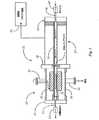
図1は、本発明による、プラズマ強化GMDS25の断面図を示す。GMDS25では、固体金属原料33は、ガスとして導入される1つまたは複数の元素と化合する。好ましい実施形態では、導入される元素の原子または分子は、反応性を増加させるために導入する前に、実質的に解離されるか、または、その他の方法で励起される。 FIG. 1 shows a cross-sectional view of a plasma enhanced
GMDS25の使用例として、固体タンタル原料およびほぼ解離した塩素を使用した、揮発性TaCl5の生産が述べられる。この例のGMDS25は、使用時点で、導管51を越えて取り付け具53を通して揮発性TaCl5を生成する。反応性金属前駆体のタイミング調整されたパルスの生成は、解離した塩素のタイミング調整された生成によって引き起こされる。反応性塩素のタイミング調整された生成は、冷却器多岐管および弁が最適条件で動作している、供給源の上流で生じ、弁を高温で動作させる必要をなくす。高電圧で高周波の電源42によって駆動されるプラズマ発生部品27は、揮発性前駆体、TaCl5を生産するために、Taとの化合時に、より高い化学反応性を得る目的で、Cl2分子をより反応性のあるCl原子に分解する、一定プラズマ源を維持するために設けられる。好ましい実施形態では、プラズマ発生器27は、この使用のためにカスタマイズされたヘリカル共振器である。炉アセンブリ29が設けられ、原料Ta33と生成したプラズマの両方を収容するようになされている石英管31内に設置される固体Ta金属原料33を加熱するようになされている。石英管31は、プラズマ発生器と固体Ta原料物質を保持する加熱領域の両方を通して延びる。As an example of the use of GMDS25 , the production of volatile TaCl5 using solid tantalum raw material and nearly dissociated chlorine is described. The
加熱要素35は、Ta33に対して直接で、かつ、調整可能な加熱源を提供する。好ましい実施形態では、炉の電力は、200〜400℃の範囲内で温度を制御するように調整される。 The
炉アセンブリ29は、フランジ43によって部品27から、同様に、端部フランジ45によってリアクタ側から分離された2重壁格納部である。しかし、共有管31の内部を通して、制限無しに自由に流れる機能が維持される。熱電対ハウジング37が設けられ、当技術分野で知られているように、炉の温度を測定する熱電対を収容するようになされている。炉アセンブリ29は、漏れを防ぐようになされた2重閉じ込め外壁36を有する。通気出口39が設けられ、当技術分野で同様に知られているように、システムの通気を可能にするようになされている。継手53および47は、それぞれ、堆積リアクタおよび上流ガス送出多岐管への接続部を提供する。 The
本発明の好ましい実施形態では、ArおよびCl2などの希ガス−ハロゲン化物混合物が2つの理由で導入される。第1は、反応相中に、TaCl5前駆体は、5〜40msec以内で、非常に速くかつ大量に生成される。ALD反応相に対する時間分解能は約100msecである。したがって、希ガスと混合することによるCl2の希釈は、過剰の前駆体の生成から保護するのに適している。第2に、例えば、Arなどの希ガスを使用することによって、プラズマが、連続して維持されることが可能になり、プラズマ生成時間がなくなる。こうして、Cl2の流れがオフされると、たとえ、連続のAr流によってプラズマがオンされ、維持されていても、Ta原料のエッチング(TaCl5の生成)が終了する。別法として、ある場合には、プラズマは、Cl2ガスの導入と一致するようにタイミング調整される。In a preferred embodiment of the present invention, a rare gas such as Ar and Cl2 - halide mixture is introduced for two reasons. First, during the reaction phase, TaCl5 precursor is produced very quickly and in large quantities within 5-40 msec. The time resolution for the ALD reaction phase is about 100 msec. Thus, dilution of Cl2 by mixing with a noble gas is suitable to protect against the formation of excess precursor. Second, by using a noble gas such as Ar, for example, the plasma can be continuously maintained, eliminating plasma generation time. Thus, when the Cl2 flow is turned off, the etching of the Ta material (generation of TaCl5 ) ends even if the plasma is turned on and maintained by the continuous Ar flow. Alternatively, in some cases, the plasma is timed to coincide with the introduction of Cl2 gas.
Cl2/希ガス混合物は、フランジ41を貫通する導管49を経由して継手47を通って管31内に導入される。混合物は、ヘリカル共振器(プラズマ生成)を通過して、一実施形態では、約20標準立方センチメートル/分(SCCM)の流量で、より反応性の高いCl原子を生成する。Cl原子は、ほぼ有効な流量で(例えば、約30sccmで)生成される。原子は、管31内でTa33と反応して、金属をエッチングし、(炉29が維持される温度で)揮発性の高いTaCl5を生成する。炉29は、生成流量より速くエッチング生成物分子を脱着することによって、Ta33を、フラックス制限モードで動作するのに十分な温度に加熱した状態に保つ。前駆体は、継手53を通ってALDリアクタ内に流れる。The Cl2 / rare gas mixture is introduced into the
以下で述べるように、汚染物質形成を抑制する方法もGMDS25によって利用される。 As will be described below, methods for suppressing pollutant formation are also utilized by
図2は、本発明の実施形態による、ALDリアクタ55およびガス源に相互接続された、図1のGMDS25を提示する断面図である。リアクタ55は、部分真空を維持し、堆積プロセス中の加熱した火床上で、基板、通常、シリコンウェハを支持する装置を有する。GMDS25は、全長が約18インチであり、事実上、任意のALDまたはCVDシステム内に容易に嵌め込み、一体化されるのに十分に小型である。この例では、GMDS25は、ALDリアクタ55に接続されて示される。 FIG. 2 is a cross-sectional view presenting the
TaCl5をリアクタ55内に送出する間、固体前駆体が、送出ラインの壁上で改質しないことが重要である。さらに、Cl原子が汚染源になる場合がある室55内に、Cl原子を通さないようにすることが同様に重要である。ニッケルめっきした送出ライン59および標準ライン加熱器57を付加することによって、これらの問題が回避される。ライン59の内側にニッケルめっきすることは、Cl原子がリアクタ55に入る前にCl原子を減少させるように働く。こうして、塩素が不注意にリアクタ55内に導入されることからの汚染が生じない。ライン59は、約90℃に加熱された状態に保たれ、前駆体が、ライン59および関連するピンチ弁61を詰まらせることを効果的に防止する。ライン59の好ましい長さは、完全にCl原子を減少させるのに十分であるものとする。さらに、TaCl5が、壁上で凝固しないようにされるため、その後の固体前駆体のフレーキングが起こらないことになり、よく知られた上流での粒子生成がなくなる。先に述べた改善によって、GMDS25を使用すると、保守の清掃時間が大幅に減る。While delivering TaCl5 into reactor 55, it is important that the solid precursor does not reform on the walls of the delivery line. Furthermore, it is equally important to keep Cl atoms out of the chamber 55 where Cl atoms can be a source of contamination. By adding a nickel-plated
GMDS25のキャリア源の端部に、4つの調整されたガスラインが示され、それぞれのラインは、特定のガスを導入する働きをする。反応性ガスおよび希ガスのタイプの選択は、固体原料のタイプの選択および所望の前駆体によって決まることになる。フッ素、臭素、および他の一般に知られている金属−エッチングガスを使用してもよい。さらに、希ガスの使用が好ましいが、場合によっては、窒素などの他のガスを使用してもよい。 At the end of the carrier source of the
GMDS25に入る反応性ガスおよび希ガスの上流の流れを調整することが重要である。そのために、標準的な弁63を、それぞれの個別のラインに設けて、ガスの流れをオンまたはオフすることが可能になる。流量絞り65を同様に設けて、それぞれの供給ラインの弁が交互に一巡するALDプロセスにおいて、流量を制限し、調量した、パルス状の流れが提供される。それぞれのラインは、流量ならびに上流圧力調整器69を調整するのに役立つ質量流量計(MFM)67を有する。当技術分野で知られているように、プラズマ制御を補助するのに、H2を使用してもよい。好ましい実施形態では、制御は、プロセスの目的に専用のソフトウェアによる。It is important to regulate the upstream flow of reactive and noble gases entering the
GMDS25の独特の実施態様は、本発明の精神および範囲から逸脱することなく、いろいろな種類の、種々の膜用のALDプロセスおよびALD応用、ならびに、CVD応用と一体化されることができることが当業者には明らかになるであろう。最適な金属原料および関連する反応物質ガスに関する研究が続き、進展するにつれて、電子デバイス用の高品質な誘電体および導電性膜の生産において商業的に使用するための、新しい将来のプロセス材料および相互作用経路を完成することができる。 It will be appreciated that the unique embodiments of GMDS 25 can be integrated with ALD processes and ALD applications for various types of films and CVD applications without departing from the spirit and scope of the present invention. It will be clear to the contractor. As research on optimal metal feedstocks and related reactant gases continues and progresses, new future process materials and mutuals for commercial use in the production of high-quality dielectric and conductive films for electronic devices The action path can be completed.
図3は、本発明の実施形態に従って、Ta2O5ALDプロセスにおいて、タンタル、塩素、およびアルゴンを使用する基本的なプロセス工程を示すプロセス流れ図である。本明細書で示すプロセス工程は、自己終了するALDサイクルを述べるが、標準的なCVDについてなど、他の応用形態では、連続した前駆体の流れを使用することができる。FIG. 3 is a process flow diagram illustrating the basic process steps using tantalum, chlorine, and argon in a Ta2 O5 ALD process in accordance with an embodiment of the present invention. The process steps shown herein describe a self-terminating ALD cycle, but in other applications, such as for standard CVD, a continuous precursor stream can be used.
工程71にて、プラズマは、点火され、アルゴンの連続流によって、安定化される。別法として、プラズマは、反応性ガスを有するパルスに対してタイミング調整されることができる。工程73にて、Cl2などの反応性ガスは、ヘリカル共振器(プラズマ生成)内に導入される。この工程では、先に述べた理由で、Cl2は、Arなどの希ガスと混合されることができる。In
工程75にて、プラズマ内で生成されたCl原子は、その後、Ta原料をエッチングして、この例では所望の前駆体である揮発性の高いTaCl5が生成される。工程77では、工程75で生成されたTaCl5は、適したALDリアクタにパルス状に入力されるか、または、別法として、適したCVDリアクタ内に連続流として導入される。明らかに、プロセスがCVDである場合、前駆体を含有する酸素は、TaCl5と同時にCVDリアクタに導入されることになる。簡略化のために、図3は、ALDプロセスに重点を置く。In
工程79にて、TaCl5は、調製された基板表面(OH)と反応して、所望のTa2O5層が生成される。工程81にて、個別のパージ(Ar)およびH2O蒸気との表面反応が行われて、金属前駆体の次のパルスについて基板表面が調製される。TaCl5の次のパルスである工程83についてサイクルが繰り返される。In
効率的で、汚染物質の無いGMDS25などのGMDSの新規の設計および実施態様によって、種々の応用について、ALD膜の作製のスループットおよび品質が大幅に改善される。固体化合物原料を使用する従来技術の応用形態では一般的である粒子汚染および洗浄要件を管理する必要に伴うダウンタイム遅延を受けることなく、好都合には、純度が高い精製されたインゴットにおいて入手しやすく、扱うのにより安全で、ガスまたは液体金属原料より一般的である固体金属原料を使用することができる。原料金属を加熱するのに低温を使用することができ、反応速度が速いため、短いパルス間隔を達成することができる。本発明の精神および範囲から逸脱することなく、プロセスに依存しない、化学物質送出源としてのGMSD25を、一般的なCVDならびにALDで使用することができる。 New designs and implementations of GMDS, such as
先の説明では、解離した塩素と共に使用され、好ましくは、アルゴンなどの希ガスと混合される固体原料として、タンタル(Ta)が述べられた。反応性ガスおよび希ガスのタイプの選択は、固体原料のタイプの選択および所望の前駆体によって決まることになることも述べられた。フッ素、臭素、および、他の一般に知られている金属−エッチングガスを使用してもよい。望まれる揮発性前駆体に応じて使用することができる種々の固体物質が同様に存在する。例えば、元素についてのよく知られている科学記号法を使用すると、本発明の実施形態における候補固体原料として以下のものをすべて考えることができる。すなわち、Ta、Zr、Hf、W、Nb、Mo、Bi、Zn、Pb、Mg、Ba、Sr、Cr、Co、P、Sr、As、Ni、Irなどである。 In the above description, tantalum (Ta) has been described as a solid source used with dissociated chlorine and preferably mixed with a noble gas such as argon. It was also mentioned that the choice of reactive gas and noble gas types will depend on the choice of solid source type and the desired precursor. Fluorine, bromine, and other commonly known metal-etching gases may be used. There are various solid materials as well, which can be used depending on the desired volatile precursor. For example, using the well-known scientific notation for elements, all of the following can be considered as candidate solid raw materials in embodiments of the present invention. That is, Ta, Zr, Hf, W, Nb, Mo, Bi, Zn, Pb, Mg, Ba, Sr, Cr, Co, P, Sr, As, Ni, Ir, and the like.
本発明の精神および範囲から逸脱することなく、先に述べた実施形態において、種々の変更を行ってもよいことも当業者には明らかになるであろう。解離(プラズマ形成)に使用される装置およびその電源は、多くの市販の、または、特注のデバイスのうちの任意のものであってよい。さらに、使用することができるいろいろな種類の金属、および、原料温度などが存在する。さらに、同様にハロゲン化物を形成する、GeおよびSiなどの元素材料が存在し、これらの材料は厳密には金属として分類されないが、本発明の操作上および機能上の範囲内で使用されることができる。さらに、種々の実施形態で述べたデバイスは、定常流のCVDプロセスに、同様に、断続流の(パルス状の)ALDプロセスに使用されることができる。さらに、ガスストリームは、原料操作時に不活性であれば、窒素などの他のキャリアガスと化合することができ、同様に、下流のウェハリアクタ領域および空間の他の不活性ガスと化合するか、または、ブレンドされることができる。通常、本発明のGMDSは、ALDリアクタまたはCVDリアクタの上流に取り付けられることになり、通常、これらの生産システムは、ALDまたはCVDリアクタ、および、プロセス中に基板を支持し加熱する加熱された火床を通して、一連の基板を順次に一巡させる装置を有する。本発明の精神および範囲は、添付特許請求項によってのみ制限される。 It will be apparent to those skilled in the art that various modifications can be made in the embodiments described above without departing from the spirit and scope of the invention. The apparatus used for dissociation (plasma formation) and its power source may be any of a number of commercially available or custom-made devices. In addition, there are various types of metals that can be used, raw material temperatures, and the like. In addition, there are elemental materials such as Ge and Si that also form halides, and these materials are not strictly classified as metals, but are used within the operational and functional scope of the present invention. Can do. Furthermore, the devices described in the various embodiments can be used for steady flow CVD processes as well as for intermittent flow (pulsed) ALD processes. In addition, the gas stream can be combined with other carrier gases such as nitrogen if it is inert during raw material operation, as well as with other inert gases in the downstream wafer reactor region and space, Or it can be blended. Typically, the GMDS of the present invention will be installed upstream of an ALD reactor or CVD reactor, and typically these production systems will support an ALD or CVD reactor and a heated fire that supports and heats the substrate during the process. It has a device that makes a series of substrates sequentially go through the floor. The spirit and scope of the present invention is limited only by the appended claims.
Claims (21)
Translated fromJapanese固体金属原料物質を保持し、処理装置に接続され、揮発性金属化合物を前記処理装置に送出する出口を有する反応室と、
前記固体金属原料物質を加熱する、反応室内の原料加熱器と、
反応性ガスを供給するガス源と、
ガス種を反応室に送出する、ガス源から反応室へのガス送出導管と、
ガス送出導管に接続する解離装置とを備え、
解離装置は、反応性ガス分子を解離し、反応室に少なくとも1つの単原子反応種を供給し、単原子反応種は、加熱された固体金属原料物質からの金属と化合し、揮発性金属化合物を形成する汎用金属送出源。A general-purpose metal delivery source for delivering a volatile metal compound to a processing device in the form of a gas,
A reaction chamber holding a solid metal source material, connected to a processing device and having an outlet for delivering a volatile metal compound to the processing device;
A raw material heater in a reaction chamber for heating the solid metal raw material,
A gas source for supplying a reactive gas;
A gas delivery conduit from the gas source to the reaction chamber for delivering gas species to the reaction chamber;
A dissociation device connected to the gas delivery conduit;
The dissociator dissociates reactive gas molecules and supplies at least one monoatomic reactive species to the reaction chamber, the monoatomic reactive species combine with the metal from the heated solid metal source material, and a volatile metal compound Forming a general-purpose metal delivery source.
(a)ガス源からの反応性ガスを、固体金属原料を保持する加熱された反応室に接続されるガス送出導管内に流す工程と、
(b)流れる反応性ガス内でプラズマを衝突させ、それによって、反応性ガスの少なくとも1つの単原子種を形成する工程と、
(c)加熱された金属原料と少なくとも1つの単原子反応性ガスとの間の化学反応を通して、反応室内に揮発性金属化合物を形成する工程と、
(d)反応室の出口で揮発性金属化合物を送出する工程とを含む方法。A method of supplying a volatile metal compound to an outlet of a reaction chamber,
(A) flowing reactive gas from a gas source through a gas delivery conduit connected to a heated reaction chamber holding a solid metal source;
(B) impinging plasma in the flowing reactive gas, thereby forming at least one monoatomic species of the reactive gas;
(C) forming a volatile metal compound in the reaction chamber through a chemical reaction between the heated metal source and at least one monoatomic reactive gas;
(D) delivering a volatile metal compound at the outlet of the reaction chamber.
プロセス堆積室内で基板を支持する加熱された火床と、
後続の処理のために、基板を交換する装置と、
コーティング室へ前駆体として揮発性金属化合物を送出する入口ポートと、
入口ポートに接続される汎用金属送出源とを備え、汎用金属送出源は、
固体金属原料物質を保持し、前記コーティング室に揮発性金属化合物を送出する出口を有する反応室と、
前記固体金属原料物質を加熱する、反応室内の加熱器と、
反応性ガスを供給するガス源と、
ガス種を反応室に送出する、ガス源から反応室へのガス送出導管と、
ガス送出導管に接続されるプラズマ発生装置とを備え、
プラズマ発生装置は、反応性ガス分子を解離し、反応室に少なくとも1つの単原子反応種を供給し、単原子反応種は、加熱された固体金属原料物質からの金属と化合し、コーティング室に送出される揮発性金属化合物を形成する処理システム。A processing system,
A heated firebed supporting the substrate in the process deposition chamber;
An apparatus for changing the substrate for subsequent processing;
An inlet port for delivering a volatile metal compound as a precursor to the coating chamber;
A universal metal delivery source connected to the inlet port,
A reaction chamber having an outlet for holding a solid metal source material and delivering a volatile metal compound to the coating chamber;
A heater in a reaction chamber for heating the solid metal source material;
A gas source for supplying a reactive gas;
A gas delivery conduit from the gas source to the reaction chamber for delivering gas species to the reaction chamber;
A plasma generator connected to the gas delivery conduit;
The plasma generator dissociates reactive gas molecules and supplies at least one monoatomic reactive species to the reaction chamber, which combines with the metal from the heated solid metal source material and enters the coating chamber. A processing system that forms volatile metal compounds to be delivered.
CVD処理のための前駆体として揮発性金属化合物を送出する入口ポートと、
入口ポートに接続される汎用金属送出源とを備え、汎用金属送出源は、固体金属原料物質を保持し、前記コーティング室に揮発性金属化合物を送出する出口を有する反応室と、前記固体金属原料物質を加熱する、反応室内の加熱器と、反応性ガスを供給するガス源と、ガス種を反応室に送出する、ガス源から反応室へのガス送出導管と、ガス送出導管に接続する解離装置とを備え、
プラズマ発生装置は、反応性ガス分子を解離し、反応室に少なくとも1つの単原子反応種を供給し、単原子反応種は、加熱された固体金属原料物質からの金属と化合し、入口ポートに送出される揮発性金属化合物を形成する化学気相堆積システム。A chemical vapor deposition (CVD) system comprising:
An inlet port for delivering a volatile metal compound as a precursor for the CVD process;
A universal metal delivery source connected to an inlet port, the universal metal delivery source holding a solid metal source material and having an outlet for delivering a volatile metal compound to the coating chamber; and the solid metal source A heater in the reaction chamber that heats the material, a gas source that supplies the reactive gas, a gas delivery conduit from the gas source to the reaction chamber that delivers gas species to the reaction chamber, and a dissociation connected to the gas delivery conduit With the device,
The plasma generator dissociates reactive gas molecules and supplies at least one monoatomic reactive species to the reaction chamber, which combines with metal from the heated solid metal source material and enters the inlet port. A chemical vapor deposition system that forms volatile metal compounds to be delivered.
ALD処理のための前駆体として揮発性金属化合物を繰り返し送出する入口ポートと、
入口ポートに接続される汎用金属送出源とを備え、汎用金属送出源は、固体金属原料物質を保持し、前記コーティング室に揮発性金属化合物を送出する出口を有する反応室と、前記固体金属原料物質を加熱する、反応室内の加熱器と、反応性ガスを供給するガス源と、ガス種を反応室に送出する、ガス源から反応室へのガス送出導管と、ガス送出導管に接続する解離装置とを備え、
プラズマ発生装置は、反応性ガス分子を解離し、反応室に少なくとも1つの単原子反応種を供給し、単原子反応種は、加熱された固体金属原料物質からの金属と化合し、入口ポートに送出される揮発性金属化合物を形成する原子層堆積システム。An atomic layer deposition (ALD) system comprising:
An inlet port that repeatedly delivers a volatile metal compound as a precursor for ALD processing;
A universal metal delivery source connected to an inlet port, the universal metal delivery source holding a solid metal source material and having an outlet for delivering a volatile metal compound to the coating chamber; and the solid metal source A heater in the reaction chamber that heats the material, a gas source that supplies the reactive gas, a gas delivery conduit from the gas source to the reaction chamber that delivers gas species to the reaction chamber, and a dissociation connected to the gas delivery conduit With the device,
The plasma generator dissociates reactive gas molecules and supplies at least one monoatomic reactive species to the reaction chamber, which combines with metal from the heated solid metal source material and enters the inlet port. An atomic layer deposition system that forms volatile metal compounds to be delivered.
ガス源からの反応性ガスを、固体金属材料を保持する加熱された反応室に接続されるガス送出導管内に流す手段と、
流れる反応性ガス内でプラズマを衝突させる手段であって、それによって、反応性ガスの少なくとも1つの単原子種を形成する、衝突させる手段と、
加熱された金属材料と少なくとも1つの単原子反応性ガスとの間の化学反応を通して、反応室内に揮発性金属化合物を形成する手段と、
反応室の出口で揮発性金属化合物を送出する手段とを含む装置。An apparatus for supplying a volatile metal compound to an outlet of a reaction chamber,
Means for flowing reactive gas from a gas source into a gas delivery conduit connected to a heated reaction chamber holding a solid metal material;
Means for impinging a plasma in a flowing reactive gas, thereby forming at least one monoatomic species of the reactive gas;
Means for forming a volatile metal compound in the reaction chamber through a chemical reaction between the heated metal material and the at least one monoatomic reactive gas;
Means for delivering a volatile metal compound at the outlet of the reaction chamber.
Applications Claiming Priority (2)
| Application Number | Priority Date | Filing Date | Title |
|---|---|---|---|
| US10/295,614US6863021B2 (en) | 2002-11-14 | 2002-11-14 | Method and apparatus for providing and integrating a general metal delivery source (GMDS) with atomic layer deposition (ALD) |
| PCT/US2003/035768WO2004044957A2 (en) | 2002-11-14 | 2003-11-10 | Method and apparatus for providing and integrating a general metal delivery source (gmds) with atomic layer deposition (ald) |
Publications (1)
| Publication Number | Publication Date |
|---|---|
| JP2006506811Atrue JP2006506811A (en) | 2006-02-23 |
Family
ID=32297256
Family Applications (1)
| Application Number | Title | Priority Date | Filing Date |
|---|---|---|---|
| JP2004551983APendingJP2006506811A (en) | 2002-11-14 | 2003-11-10 | Method and apparatus for providing a universal metal delivery source (GMDS) and integrating the universal metal delivery source with atomic layer deposition (ALD) |
Country Status (6)
| Country | Link |
|---|---|
| US (2) | US6863021B2 (en) |
| EP (1) | EP1560945A2 (en) |
| JP (1) | JP2006506811A (en) |
| KR (1) | KR20050063807A (en) |
| AU (1) | AU2003290694A1 (en) |
| WO (1) | WO2004044957A2 (en) |
Cited By (1)
| Publication number | Priority date | Publication date | Assignee | Title |
|---|---|---|---|---|
| WO2007058120A1 (en)* | 2005-11-18 | 2007-05-24 | Hitachi Kokusai Electric Inc. | Process for producing semiconductor device and substrate treatment apparatus |
Families Citing this family (21)
| Publication number | Priority date | Publication date | Assignee | Title |
|---|---|---|---|---|
| US6921062B2 (en) | 2002-07-23 | 2005-07-26 | Advanced Technology Materials, Inc. | Vaporizer delivery ampoule |
| US7767363B2 (en)* | 2005-06-24 | 2010-08-03 | Micron Technology, Inc. | Methods for photo-processing photo-imageable material |
| KR101124504B1 (en)* | 2005-09-22 | 2012-03-15 | 삼성전자주식회사 | Fabrication method of amorphous NiO thin film by ALD process and nonvolatile memory device using the amorphous NiO thin film |
| US7582562B2 (en) | 2005-10-06 | 2009-09-01 | Micron Technology, Inc. | Atomic layer deposition methods |
| US20090087967A1 (en)* | 2005-11-14 | 2009-04-02 | Todd Michael A | Precursors and processes for low temperature selective epitaxial growth |
| US7442413B2 (en)* | 2005-11-18 | 2008-10-28 | Daystar Technologies, Inc. | Methods and apparatus for treating a work piece with a vaporous element |
| WO2007106076A2 (en)* | 2006-03-03 | 2007-09-20 | Prasad Gadgil | Apparatus and method for large area multi-layer atomic layer chemical vapor processing of thin films |
| US20080241805A1 (en)* | 2006-08-31 | 2008-10-02 | Q-Track Corporation | System and method for simulated dosimetry using a real time locating system |
| US7692222B2 (en)* | 2006-11-07 | 2010-04-06 | Raytheon Company | Atomic layer deposition in the formation of gate structures for III-V semiconductor |
| US7999479B2 (en)* | 2009-04-16 | 2011-08-16 | Varian Semiconductor Equipment Associates, Inc. | Conjugated ICP and ECR plasma sources for wide ribbon ion beam generation and control |
| EP2755453B1 (en)* | 2011-09-09 | 2019-08-07 | Toshiba Mitsubishi-Electric Industrial Systems Corporation | Plasma generator and cvd device |
| JP2015519478A (en) | 2012-05-31 | 2015-07-09 | アドバンスド テクノロジー マテリアルズ,インコーポレイテッド | Fluid delivery based on source reagent with high material flux for batch deposition |
| JP2014053477A (en)* | 2012-09-07 | 2014-03-20 | Philtech Inc | Solid metal gas supply device |
| KR101541361B1 (en)* | 2013-07-15 | 2015-08-03 | 광주과학기술원 | Fluidized bed ald appratus for nano-coated particle |
| US20170309490A1 (en)* | 2014-09-24 | 2017-10-26 | Hitachi Kokusai Electric Inc. | Method of manufacturing semiconductor device |
| US9972501B1 (en) | 2017-03-14 | 2018-05-15 | Nano-Master, Inc. | Techniques and systems for continuous-flow plasma enhanced atomic layer deposition (PEALD) |
| CN111295462A (en)* | 2017-10-12 | 2020-06-16 | 盖列斯特科技股份有限公司 | Method and system for integrated synthesis, delivery, and processing of source chemicals in thin film manufacturing |
| US11087959B2 (en) | 2020-01-09 | 2021-08-10 | Nano-Master, Inc. | Techniques for a hybrid design for efficient and economical plasma enhanced atomic layer deposition (PEALD) and plasma enhanced chemical vapor deposition (PECVD) |
| US11640900B2 (en) | 2020-02-12 | 2023-05-02 | Nano-Master, Inc. | Electron cyclotron rotation (ECR)-enhanced hollow cathode plasma source (HCPS) |
| US12197125B2 (en) | 2020-12-22 | 2025-01-14 | Nano-Master, Inc. | Mask and reticle protection with atomic layer deposition (ALD) |
| US12180586B2 (en) | 2021-08-13 | 2024-12-31 | NanoMaster, Inc. | Apparatus and methods for roll-to-roll (R2R) plasma enhanced/activated atomic layer deposition (PEALD/PAALD) |
Family Cites Families (11)
| Publication number | Priority date | Publication date | Assignee | Title |
|---|---|---|---|---|
| US3614658A (en)* | 1969-01-22 | 1971-10-19 | Spectra Physics | Gas laser having means for maintaining a uniform gas mixture in a dc discharge |
| US4699082A (en)* | 1983-02-25 | 1987-10-13 | Liburdi Engineering Limited | Apparatus for chemical vapor deposition |
| US4945857A (en)* | 1986-03-14 | 1990-08-07 | International Business Machines Corporation | Plasma formation of hydride compounds |
| US4971832A (en)* | 1988-03-02 | 1990-11-20 | Canon Kabushiki Kaisha | HR-CVD process for the formation of a functional deposited film on a substrate with application of a voltage in the range of -5 to -100 V |
| JP3231426B2 (en)* | 1992-10-28 | 2001-11-19 | 富士通株式会社 | Hydrogen plasma downflow processing method and hydrogen plasma downflow processing apparatus |
| JP2793472B2 (en)* | 1993-06-24 | 1998-09-03 | 日本電気株式会社 | Copper fine processing method and copper fine processing apparatus |
| US6143081A (en)* | 1996-07-12 | 2000-11-07 | Tokyo Electron Limited | Film forming apparatus and method, and film modifying apparatus and method |
| US6071572A (en)* | 1996-10-15 | 2000-06-06 | Applied Materials, Inc. | Forming tin thin films using remote activated specie generation |
| US6112696A (en)* | 1998-02-17 | 2000-09-05 | Dry Plasma Systems, Inc. | Downstream plasma using oxygen gas mixture |
| US6225745B1 (en)* | 1999-12-17 | 2001-05-01 | Axcelis Technologies, Inc. | Dual plasma source for plasma process chamber |
| US6720259B2 (en)* | 2001-10-02 | 2004-04-13 | Genus, Inc. | Passivation method for improved uniformity and repeatability for atomic layer deposition and chemical vapor deposition |
- 2002
- 2002-11-14USUS10/295,614patent/US6863021B2/ennot_activeExpired - Lifetime
- 2003
- 2003-11-10KRKR1020057008594Apatent/KR20050063807A/ennot_activeCeased
- 2003-11-10JPJP2004551983Apatent/JP2006506811A/enactivePending
- 2003-11-10EPEP03783276Apatent/EP1560945A2/ennot_activeWithdrawn
- 2003-11-10AUAU2003290694Apatent/AU2003290694A1/ennot_activeAbandoned
- 2003-11-10WOPCT/US2003/035768patent/WO2004044957A2/ennot_activeApplication Discontinuation
- 2004
- 2004-12-15USUS11/014,104patent/US20050103269A1/ennot_activeAbandoned
Cited By (3)
| Publication number | Priority date | Publication date | Assignee | Title |
|---|---|---|---|---|
| WO2007058120A1 (en)* | 2005-11-18 | 2007-05-24 | Hitachi Kokusai Electric Inc. | Process for producing semiconductor device and substrate treatment apparatus |
| US7968437B2 (en) | 2005-11-18 | 2011-06-28 | Hitachi Kokusai Electric Inc. | Semiconductor device manufacturing method and substrate processing apparatus |
| JP5097554B2 (en)* | 2005-11-18 | 2012-12-12 | 株式会社日立国際電気 | Semiconductor device manufacturing method, substrate processing method, and substrate processing apparatus |
Also Published As
| Publication number | Publication date |
|---|---|
| AU2003290694A8 (en) | 2004-06-03 |
| WO2004044957A2 (en) | 2004-05-27 |
| EP1560945A2 (en) | 2005-08-10 |
| US20050103269A1 (en) | 2005-05-19 |
| WO2004044957A3 (en) | 2004-10-07 |
| US6863021B2 (en) | 2005-03-08 |
| AU2003290694A1 (en) | 2004-06-03 |
| KR20050063807A (en) | 2005-06-28 |
| US20040094093A1 (en) | 2004-05-20 |
Similar Documents
| Publication | Publication Date | Title |
|---|---|---|
| JP2006506811A (en) | Method and apparatus for providing a universal metal delivery source (GMDS) and integrating the universal metal delivery source with atomic layer deposition (ALD) | |
| US6305314B1 (en) | Apparatus and concept for minimizing parasitic chemical vapor deposition during atomic layer deposition | |
| US6540838B2 (en) | Apparatus and concept for minimizing parasitic chemical vapor deposition during atomic layer deposition | |
| CN101063196B (en) | Atomic layer deposition method and apparatus using solution-based precursors | |
| US7713592B2 (en) | Nanolayer deposition process | |
| US6773507B2 (en) | Apparatus and method for fast-cycle atomic layer deposition | |
| US20050136657A1 (en) | Film-formation method for semiconductor process | |
| US20050223982A1 (en) | Apparatus and method for depositing thin film on wafer using remote plasma | |
| US20100266765A1 (en) | Method and apparatus for growing a thin film onto a substrate | |
| JP2003508932A (en) | Improved apparatus and method for growing thin films | |
| JP2004356612A (en) | Passivation method to improve uniformity and reproducibility of atomic layer deposition and chemical vapor deposition | |
| KR100606398B1 (en) | Film deposition method for semiconductor processing | |
| KR20090013111A (en) | In-situ deposition method of different metal-containing films using cyclopentadienyl metal precursors | |
| JP2007270355A (en) | Method and system for initiating a deposition process utilizing a metal carbonyl precursor | |
| EP2047009B1 (en) | Methods and apparatus for the vaporization and delivery of solution precursors for atomic layer deposition | |
| JP4965260B2 (en) | A method of depositing a metal layer using sequential flow deposition. | |
| US20210371978A1 (en) | System and methods for direct liquid injection of vanadium precursors | |
| JP4356943B2 (en) | Substrate processing apparatus and semiconductor device manufacturing method | |
| US11515154B2 (en) | Selective deposition of a passivation film |
Legal Events
| Date | Code | Title | Description |
|---|---|---|---|
| A977 | Report on retrieval | Free format text:JAPANESE INTERMEDIATE CODE: A971007 Effective date:20081023 | |
| A131 | Notification of reasons for refusal | Free format text:JAPANESE INTERMEDIATE CODE: A131 Effective date:20081111 | |
| A601 | Written request for extension of time | Free format text:JAPANESE INTERMEDIATE CODE: A601 Effective date:20090205 | |
| A602 | Written permission of extension of time | Free format text:JAPANESE INTERMEDIATE CODE: A602 Effective date:20090213 | |
| A521 | Request for written amendment filed | Free format text:JAPANESE INTERMEDIATE CODE: A523 Effective date:20090427 | |
| A02 | Decision of refusal | Free format text:JAPANESE INTERMEDIATE CODE: A02 Effective date:20090526 |