JP2006502578A - Electronic device with phase change material - Google Patents
Electronic device with phase change materialDownload PDFInfo
- Publication number
- JP2006502578A JP2006502578AJP2004542691AJP2004542691AJP2006502578AJP 2006502578 AJP2006502578 AJP 2006502578AJP 2004542691 AJP2004542691 AJP 2004542691AJP 2004542691 AJP2004542691 AJP 2004542691AJP 2006502578 AJP2006502578 AJP 2006502578A
- Authority
- JP
- Japan
- Prior art keywords
- electronic device
- phase
- region
- conductor
- layer
- Prior art date
- Legal status (The legal status is an assumption and is not a legal conclusion. Google has not performed a legal analysis and makes no representation as to the accuracy of the status listed.)
- Withdrawn
Links
- 239000012782phase change materialSubstances0.000titleclaimsabstractdescription61
- 239000004020conductorSubstances0.000claimsabstractdescription75
- 239000011148porous materialSubstances0.000claimsabstractdescription75
- 238000010438heat treatmentMethods0.000claimsabstractdescription28
- 230000007704transitionEffects0.000claimsabstractdescription19
- 230000015654memoryEffects0.000claimsdescription52
- 239000004094surface-active agentSubstances0.000claimsdescription26
- 239000003989dielectric materialSubstances0.000claimsdescription23
- 239000004065semiconductorSubstances0.000claimsdescription13
- 239000000758substrateSubstances0.000claimsdescription13
- 230000002209hydrophobic effectEffects0.000claimsdescription12
- 125000001183hydrocarbyl groupChemical group0.000claimsdescription11
- 230000005669field effectEffects0.000claimsdescription10
- 239000002904solventSubstances0.000claimsdescription10
- 230000005661hydrophobic surfaceEffects0.000claimsdescription8
- 229910044991metal oxideInorganic materials0.000claimsdescription8
- 150000004706metal oxidesChemical class0.000claimsdescription8
- 239000002253acidSubstances0.000claimsdescription6
- 239000007788liquidSubstances0.000claimsdescription6
- 239000003093cationic surfactantSubstances0.000claimsdescription4
- 239000000203mixtureSubstances0.000description33
- 239000000463materialSubstances0.000description32
- VYPSYNLAJGMNEJ-UHFFFAOYSA-NSilicium dioxideChemical compoundO=[Si]=OVYPSYNLAJGMNEJ-UHFFFAOYSA-N0.000description23
- LFQSCWFLJHTTHZ-UHFFFAOYSA-NEthanolChemical compoundCCOLFQSCWFLJHTTHZ-UHFFFAOYSA-N0.000description15
- 239000000377silicon dioxideSubstances0.000description13
- XQMTUIZTZJXUFM-UHFFFAOYSA-Ntetraethoxy silicateChemical compoundCCOO[Si](OOCC)(OOCC)OOCCXQMTUIZTZJXUFM-UHFFFAOYSA-N0.000description11
- BFXIKLCIZHOAAZ-UHFFFAOYSA-NmethyltrimethoxysilaneChemical compoundCO[Si](C)(OC)OCBFXIKLCIZHOAAZ-UHFFFAOYSA-N0.000description10
- LZZYPRNAOMGNLH-UHFFFAOYSA-MCetrimonium bromideChemical compound[Br-].CCCCCCCCCCCCCCCC[N+](C)(C)CLZZYPRNAOMGNLH-UHFFFAOYSA-M0.000description8
- 238000004519manufacturing processMethods0.000description8
- XUIMIQQOPSSXEZ-UHFFFAOYSA-NSiliconChemical compound[Si]XUIMIQQOPSSXEZ-UHFFFAOYSA-N0.000description7
- 229910052710siliconInorganic materials0.000description7
- XLYOFNOQVPJJNP-UHFFFAOYSA-NwaterChemical compoundOXLYOFNOQVPJJNP-UHFFFAOYSA-N0.000description7
- 238000002955isolationMethods0.000description6
- 239000010703siliconSubstances0.000description6
- 229920003171Poly (ethylene oxide)Polymers0.000description5
- 125000003545alkoxy groupChemical group0.000description5
- 238000000034methodMethods0.000description5
- 235000012239silicon dioxideNutrition0.000description5
- 125000006850spacer groupChemical group0.000description5
- 238000004528spin coatingMethods0.000description5
- OKTJSMMVPCPJKN-UHFFFAOYSA-NCarbonChemical compound[C]OKTJSMMVPCPJKN-UHFFFAOYSA-N0.000description4
- 239000012298atmosphereSubstances0.000description4
- 229910052799carbonInorganic materials0.000description4
- 229920001451polypropylene glycolPolymers0.000description4
- WFKWXMTUELFFGS-UHFFFAOYSA-NtungstenChemical compound[W]WFKWXMTUELFFGS-UHFFFAOYSA-N0.000description4
- 229910052721tungstenInorganic materials0.000description4
- 239000010937tungstenSubstances0.000description4
- OKKJLVBELUTLKV-UHFFFAOYSA-NMethanolChemical compoundOCOKKJLVBELUTLKV-UHFFFAOYSA-N0.000description3
- ZOKXTWBITQBERF-UHFFFAOYSA-NMolybdenumChemical compound[Mo]ZOKXTWBITQBERF-UHFFFAOYSA-N0.000description3
- GWEVSGVZZGPLCZ-UHFFFAOYSA-NTitan oxideChemical compoundO=[Ti]=OGWEVSGVZZGPLCZ-UHFFFAOYSA-N0.000description3
- XHCLAFWTIXFWPH-UHFFFAOYSA-N[O-2].[O-2].[O-2].[O-2].[O-2].[V+5].[V+5]Chemical compound[O-2].[O-2].[O-2].[O-2].[O-2].[V+5].[V+5]XHCLAFWTIXFWPH-UHFFFAOYSA-N0.000description3
- 125000003118aryl groupChemical group0.000description3
- 230000004888barrier functionEffects0.000description3
- 230000008901benefitEffects0.000description3
- 239000013078crystalSubstances0.000description3
- 238000009792diffusion processMethods0.000description3
- 230000000694effectsEffects0.000description3
- 238000005516engineering processMethods0.000description3
- 238000002474experimental methodMethods0.000description3
- 230000002349favourable effectEffects0.000description3
- 230000006870functionEffects0.000description3
- 229910052750molybdenumInorganic materials0.000description3
- 239000011733molybdenumSubstances0.000description3
- RVTZCBVAJQQJTK-UHFFFAOYSA-Noxygen(2-);zirconium(4+)Chemical compound[O-2].[O-2].[Zr+4]RVTZCBVAJQQJTK-UHFFFAOYSA-N0.000description3
- 229920001992poloxamer 407Polymers0.000description3
- 229910021426porous siliconInorganic materials0.000description3
- 239000000126substanceSubstances0.000description3
- OGIDPMRJRNCKJF-UHFFFAOYSA-Ntitanium oxideInorganic materials[Ti]=OOGIDPMRJRNCKJF-UHFFFAOYSA-N0.000description3
- 229910001935vanadium oxideInorganic materials0.000description3
- 229910001928zirconium oxideInorganic materials0.000description3
- IJGRMHOSHXDMSA-UHFFFAOYSA-NAtomic nitrogenChemical compoundN#NIJGRMHOSHXDMSA-UHFFFAOYSA-N0.000description2
- 102100021439Cancer/testis antigen 62Human genes0.000description2
- 101710117701Cancer/testis antigen 62Proteins0.000description2
- RYGMFSIKBFXOCR-UHFFFAOYSA-NCopperChemical compound[Cu]RYGMFSIKBFXOCR-UHFFFAOYSA-N0.000description2
- RTZKZFJDLAIYFH-UHFFFAOYSA-NDiethyl etherChemical compoundCCOCCRTZKZFJDLAIYFH-UHFFFAOYSA-N0.000description2
- LRHPLDYGYMQRHN-UHFFFAOYSA-NN-ButanolChemical compoundCCCCOLRHPLDYGYMQRHN-UHFFFAOYSA-N0.000description2
- NRTOMJZYCJJWKI-UHFFFAOYSA-NTitanium nitrideChemical compound[Ti]#NNRTOMJZYCJJWKI-UHFFFAOYSA-N0.000description2
- 238000010306acid treatmentMethods0.000description2
- 125000000217alkyl groupChemical group0.000description2
- 229910052782aluminiumInorganic materials0.000description2
- XAGFODPZIPBFFR-UHFFFAOYSA-NaluminiumChemical compound[Al]XAGFODPZIPBFFR-UHFFFAOYSA-N0.000description2
- 229910052787antimonyInorganic materials0.000description2
- QVGXLLKOCUKJST-UHFFFAOYSA-Natomic oxygenChemical compound[O]QVGXLLKOCUKJST-UHFFFAOYSA-N0.000description2
- 239000002775capsuleSubstances0.000description2
- 230000008859changeEffects0.000description2
- 229910052802copperInorganic materials0.000description2
- 239000010949copperSubstances0.000description2
- 238000005260corrosionMethods0.000description2
- 230000007797corrosionEffects0.000description2
- 230000008878couplingEffects0.000description2
- 238000010168coupling processMethods0.000description2
- 238000005859coupling reactionMethods0.000description2
- DTPCFIHYWYONMD-UHFFFAOYSA-Ndecaethylene glycolPolymersOCCOCCOCCOCCOCCOCCOCCOCCOCCOCCODTPCFIHYWYONMD-UHFFFAOYSA-N0.000description2
- 238000000151depositionMethods0.000description2
- 238000010304firingMethods0.000description2
- 229910052739hydrogenInorganic materials0.000description2
- 239000000155meltSubstances0.000description2
- 125000002496methyl groupChemical group[H]C([H])([H])*0.000description2
- 239000012229microporous materialSubstances0.000description2
- 229910052757nitrogenInorganic materials0.000description2
- 229910052760oxygenInorganic materials0.000description2
- 239000001301oxygenSubstances0.000description2
- 125000001997phenyl groupChemical group[H]C1=C([H])C([H])=C(*)C([H])=C1[H]0.000description2
- 238000012545processingMethods0.000description2
- 238000005001rutherford backscattering spectroscopyMethods0.000description2
- 229910052723transition metalInorganic materials0.000description2
- 150000003624transition metalsChemical class0.000description2
- CPUDPFPXCZDNGI-UHFFFAOYSA-Ntriethoxy(methyl)silaneChemical compoundCCO[Si](C)(OCC)OCCCPUDPFPXCZDNGI-UHFFFAOYSA-N0.000description2
- JCVQKRGIASEUKR-UHFFFAOYSA-Ntriethoxy(phenyl)silaneChemical compoundCCO[Si](OCC)(OCC)C1=CC=CC=C1JCVQKRGIASEUKR-UHFFFAOYSA-N0.000description2
- 238000009489vacuum treatmentMethods0.000description2
- CMCBDXRRFKYBDG-UHFFFAOYSA-N1-dodecoxydodecaneChemical compoundCCCCCCCCCCCCOCCCCCCCCCCCCCMCBDXRRFKYBDG-UHFFFAOYSA-N0.000description1
- VBICKXHEKHSIBG-UHFFFAOYSA-N1-monostearoylglycerolChemical compoundCCCCCCCCCCCCCCCCCC(=O)OCC(O)COVBICKXHEKHSIBG-UHFFFAOYSA-N0.000description1
- HBXWUCXDUUJDRB-UHFFFAOYSA-N1-octadecoxyoctadecaneChemical compoundCCCCCCCCCCCCCCCCCCOCCCCCCCCCCCCCCCCCCHBXWUCXDUUJDRB-UHFFFAOYSA-N0.000description1
- HNUQMTZUNUBOLQ-UHFFFAOYSA-N2-[2-[2-[2-[2-[2-[2-[2-[2-(2-octadecoxyethoxy)ethoxy]ethoxy]ethoxy]ethoxy]ethoxy]ethoxy]ethoxy]ethoxy]ethanolChemical compoundCCCCCCCCCCCCCCCCCCOCCOCCOCCOCCOCCOCCOCCOCCOCCOCCOHNUQMTZUNUBOLQ-UHFFFAOYSA-N0.000description1
- 229910001218Gallium arsenideInorganic materials0.000description1
- DCXXMTOCNZCJGO-UHFFFAOYSA-NGlycerol trioctadecanoateNatural productsCCCCCCCCCCCCCCCCCC(=O)OCC(OC(=O)CCCCCCCCCCCCCCCCC)COC(=O)CCCCCCCCCCCCCCCCCDCXXMTOCNZCJGO-UHFFFAOYSA-N0.000description1
- VEXZGXHMUGYJMC-UHFFFAOYSA-NHydrochloric acidChemical compoundClVEXZGXHMUGYJMC-UHFFFAOYSA-N0.000description1
- UFHFLCQGNIYNRP-UHFFFAOYSA-NHydrogenChemical compound[H][H]UFHFLCQGNIYNRP-UHFFFAOYSA-N0.000description1
- 239000004642PolyimideSubstances0.000description1
- 229910052581Si3N4Inorganic materials0.000description1
- BLRPTPMANUNPDV-UHFFFAOYSA-NSilaneChemical compound[SiH4]BLRPTPMANUNPDV-UHFFFAOYSA-N0.000description1
- RTAQQCXQSZGOHL-UHFFFAOYSA-NTitaniumChemical compound[Ti]RTAQQCXQSZGOHL-UHFFFAOYSA-N0.000description1
- 238000002441X-ray diffractionMethods0.000description1
- UGACIEPFGXRWCH-UHFFFAOYSA-N[Si].[Ti]Chemical compound[Si].[Ti]UGACIEPFGXRWCH-UHFFFAOYSA-N0.000description1
- 238000010521absorption reactionMethods0.000description1
- 230000009471actionEffects0.000description1
- 230000002730additional effectEffects0.000description1
- 230000032683agingEffects0.000description1
- 150000001298alcoholsChemical class0.000description1
- UQZIWOQVLUASCR-UHFFFAOYSA-Nalumane;titaniumChemical compound[AlH3].[Ti]UQZIWOQVLUASCR-UHFFFAOYSA-N0.000description1
- 125000000129anionic groupChemical group0.000description1
- 239000003945anionic surfactantSubstances0.000description1
- GQVVQDJHRQBZNG-UHFFFAOYSA-Nbenzyl(trimethoxy)silaneChemical compoundCO[Si](OC)(OC)CC1=CC=CC=C1GQVVQDJHRQBZNG-UHFFFAOYSA-N0.000description1
- 230000015572biosynthetic processEffects0.000description1
- 229920001400block copolymerPolymers0.000description1
- 239000005380borophosphosilicate glassSubstances0.000description1
- -1butoxy, propoxy, ethoxyChemical group0.000description1
- 230000015556catabolic processEffects0.000description1
- 239000003054catalystSubstances0.000description1
- 125000002091cationic groupChemical group0.000description1
- 238000004132cross linkingMethods0.000description1
- 238000006297dehydration reactionMethods0.000description1
- 230000008021depositionEffects0.000description1
- 238000013461designMethods0.000description1
- 238000010790dilutionMethods0.000description1
- 239000012895dilutionSubstances0.000description1
- YYLGKUPAFFKGRQ-UHFFFAOYSA-NdimethyldiethoxysilaneChemical compoundCCO[Si](C)(C)OCCYYLGKUPAFFKGRQ-UHFFFAOYSA-N0.000description1
- 238000001035dryingMethods0.000description1
- 238000005530etchingMethods0.000description1
- 150000002170ethersChemical class0.000description1
- 125000001495ethyl groupChemical group[H]C([H])([H])C([H])([H])*0.000description1
- 238000003682fluorination reactionMethods0.000description1
- 239000007789gasSubstances0.000description1
- 239000011521glassSubstances0.000description1
- 239000001257hydrogenSubstances0.000description1
- 229910000041hydrogen chlorideInorganic materials0.000description1
- IXCSERBJSXMMFS-UHFFFAOYSA-Nhydrogen chlorideSubstancesCl.ClIXCSERBJSXMMFS-UHFFFAOYSA-N0.000description1
- 230000007062hydrolysisEffects0.000description1
- 238000006460hydrolysis reactionMethods0.000description1
- 230000010354integrationEffects0.000description1
- 230000002452interceptive effectEffects0.000description1
- CNQCVBJFEGMYDW-UHFFFAOYSA-Nlawrencium atomChemical compound[Lr]CNQCVBJFEGMYDW-UHFFFAOYSA-N0.000description1
- 239000011159matrix materialSubstances0.000description1
- 238000005259measurementMethods0.000description1
- 230000008018meltingEffects0.000description1
- 238000002844meltingMethods0.000description1
- 230000028161membrane depolarizationEffects0.000description1
- QSHDDOUJBYECFT-UHFFFAOYSA-NmercuryChemical compound[Hg]QSHDDOUJBYECFT-UHFFFAOYSA-N0.000description1
- 229910052753mercuryInorganic materials0.000description1
- 229910052751metalInorganic materials0.000description1
- 239000002184metalSubstances0.000description1
- 150000002739metalsChemical class0.000description1
- 125000000956methoxy groupChemical group[H]C([H])([H])O*0.000description1
- 229910021421monocrystalline siliconInorganic materials0.000description1
- 239000002736nonionic surfactantSubstances0.000description1
- 239000004033plasticSubstances0.000description1
- 229920003023plasticPolymers0.000description1
- 229910021420polycrystalline siliconInorganic materials0.000description1
- 229920001721polyimidePolymers0.000description1
- 229920000642polymerPolymers0.000description1
- 229920005591polysiliconPolymers0.000description1
- BDERNNFJNOPAEC-UHFFFAOYSA-Npropan-1-olChemical compoundCCCOBDERNNFJNOPAEC-UHFFFAOYSA-N0.000description1
- 239000000523sampleSubstances0.000description1
- 230000035945sensitivityEffects0.000description1
- 238000000926separation methodMethods0.000description1
- 229910000077silaneInorganic materials0.000description1
- 125000005372silanol groupChemical group0.000description1
- HQVNEWCFYHHQES-UHFFFAOYSA-Nsilicon nitrideChemical compoundN12[Si]34N5[Si]62N3[Si]51N64HQVNEWCFYHHQES-UHFFFAOYSA-N0.000description1
- 238000003756stirringMethods0.000description1
- 229910052719titaniumInorganic materials0.000description1
- 239000010936titaniumSubstances0.000description1
- 229910021341titanium silicideInorganic materials0.000description1
- MAKDTFFYCIMFQP-UHFFFAOYSA-Ntitanium tungstenChemical compound[Ti].[W]MAKDTFFYCIMFQP-UHFFFAOYSA-N0.000description1
- 229920000428triblock copolymerPolymers0.000description1
- ILWRPSCZWQJDMK-UHFFFAOYSA-Ntriethylazanium;chlorideChemical compoundCl.CCN(CC)CCILWRPSCZWQJDMK-UHFFFAOYSA-N0.000description1
- WQJQOUPTWCFRMM-UHFFFAOYSA-Ntungsten disilicideChemical compound[Si]#[W]#[Si]WQJQOUPTWCFRMM-UHFFFAOYSA-N0.000description1
- 229910021342tungsten silicideInorganic materials0.000description1
Images

Classifications
- H—ELECTRICITY
- H10—SEMICONDUCTOR DEVICES; ELECTRIC SOLID-STATE DEVICES NOT OTHERWISE PROVIDED FOR
- H10B—ELECTRONIC MEMORY DEVICES
- H10B63/00—Resistance change memory devices, e.g. resistive RAM [ReRAM] devices
- H10B63/20—Resistance change memory devices, e.g. resistive RAM [ReRAM] devices comprising selection components having two electrodes, e.g. diodes
- H—ELECTRICITY
- H10—SEMICONDUCTOR DEVICES; ELECTRIC SOLID-STATE DEVICES NOT OTHERWISE PROVIDED FOR
- H10N—ELECTRIC SOLID-STATE DEVICES NOT OTHERWISE PROVIDED FOR
- H10N70/00—Solid-state devices having no potential barriers, and specially adapted for rectifying, amplifying, oscillating or switching
- H10N70/20—Multistable switching devices, e.g. memristors
- H10N70/231—Multistable switching devices, e.g. memristors based on solid-state phase change, e.g. between amorphous and crystalline phases, Ovshinsky effect
- H—ELECTRICITY
- H10—SEMICONDUCTOR DEVICES; ELECTRIC SOLID-STATE DEVICES NOT OTHERWISE PROVIDED FOR
- H10D—INORGANIC ELECTRIC SEMICONDUCTOR DEVICES
- H10D84/00—Integrated devices formed in or on semiconductor substrates that comprise only semiconducting layers, e.g. on Si wafers or on GaAs-on-Si wafers
- H—ELECTRICITY
- H10—SEMICONDUCTOR DEVICES; ELECTRIC SOLID-STATE DEVICES NOT OTHERWISE PROVIDED FOR
- H10B—ELECTRONIC MEMORY DEVICES
- H10B63/00—Resistance change memory devices, e.g. resistive RAM [ReRAM] devices
- H10B63/30—Resistance change memory devices, e.g. resistive RAM [ReRAM] devices comprising selection components having three or more electrodes, e.g. transistors
- H—ELECTRICITY
- H10—SEMICONDUCTOR DEVICES; ELECTRIC SOLID-STATE DEVICES NOT OTHERWISE PROVIDED FOR
- H10D—INORGANIC ELECTRIC SEMICONDUCTOR DEVICES
- H10D84/00—Integrated devices formed in or on semiconductor substrates that comprise only semiconducting layers, e.g. on Si wafers or on GaAs-on-Si wafers
- H10D84/80—Integrated devices formed in or on semiconductor substrates that comprise only semiconducting layers, e.g. on Si wafers or on GaAs-on-Si wafers characterised by the integration of at least one component covered by groups H10D12/00 or H10D30/00, e.g. integration of IGFETs
- H—ELECTRICITY
- H10—SEMICONDUCTOR DEVICES; ELECTRIC SOLID-STATE DEVICES NOT OTHERWISE PROVIDED FOR
- H10N—ELECTRIC SOLID-STATE DEVICES NOT OTHERWISE PROVIDED FOR
- H10N70/00—Solid-state devices having no potential barriers, and specially adapted for rectifying, amplifying, oscillating or switching
- H10N70/801—Constructional details of multistable switching devices
- H10N70/821—Device geometry
- H10N70/826—Device geometry adapted for essentially vertical current flow, e.g. sandwich or pillar type devices
- H—ELECTRICITY
- H10—SEMICONDUCTOR DEVICES; ELECTRIC SOLID-STATE DEVICES NOT OTHERWISE PROVIDED FOR
- H10N—ELECTRIC SOLID-STATE DEVICES NOT OTHERWISE PROVIDED FOR
- H10N70/00—Solid-state devices having no potential barriers, and specially adapted for rectifying, amplifying, oscillating or switching
- H10N70/801—Constructional details of multistable switching devices
- H10N70/841—Electrodes
- H10N70/8413—Electrodes adapted for resistive heating
- H—ELECTRICITY
- H10—SEMICONDUCTOR DEVICES; ELECTRIC SOLID-STATE DEVICES NOT OTHERWISE PROVIDED FOR
- H10N—ELECTRIC SOLID-STATE DEVICES NOT OTHERWISE PROVIDED FOR
- H10N70/00—Solid-state devices having no potential barriers, and specially adapted for rectifying, amplifying, oscillating or switching
- H10N70/801—Constructional details of multistable switching devices
- H10N70/861—Thermal details
- H10N70/8616—Thermal insulation means
- H—ELECTRICITY
- H10—SEMICONDUCTOR DEVICES; ELECTRIC SOLID-STATE DEVICES NOT OTHERWISE PROVIDED FOR
- H10N—ELECTRIC SOLID-STATE DEVICES NOT OTHERWISE PROVIDED FOR
- H10N70/00—Solid-state devices having no potential barriers, and specially adapted for rectifying, amplifying, oscillating or switching
- H10N70/801—Constructional details of multistable switching devices
- H10N70/881—Switching materials
- H10N70/882—Compounds of sulfur, selenium or tellurium, e.g. chalcogenides
- H10N70/8828—Tellurides, e.g. GeSbTe
- G—PHYSICS
- G11—INFORMATION STORAGE
- G11C—STATIC STORES
- G11C13/00—Digital stores characterised by the use of storage elements not covered by groups G11C11/00, G11C23/00, or G11C25/00
- G11C13/0002—Digital stores characterised by the use of storage elements not covered by groups G11C11/00, G11C23/00, or G11C25/00 using resistive RAM [RRAM] elements
- G11C13/0004—Digital stores characterised by the use of storage elements not covered by groups G11C11/00, G11C23/00, or G11C25/00 using resistive RAM [RRAM] elements comprising amorphous/crystalline phase transition cells
Landscapes
- Semiconductor Memories (AREA)
- Developing Agents For Electrophotography (AREA)
- Discharge Heating (AREA)
- Internal Circuitry In Semiconductor Integrated Circuit Devices (AREA)
- Formation Of Insulating Films (AREA)
- Waveguide Switches, Polarizers, And Phase Shifters (AREA)
- Inorganic Insulating Materials (AREA)
- Resistance Heating (AREA)
- Thermistors And Varistors (AREA)
Abstract
Translated fromJapaneseDescription
Translated fromJapaneseこの発明は、第一の相と第二の相とを取りえる相変化材料を備えたレジスタを有する本体を備えた電子装置であって、前記レジスタは第一のコンタクト領域と第二のコンタクト領域とを備えた表面を有し、前記レジスタは前記第一のコンタクト領域と前記第二のコンタクト領域との間で電気的抵抗を有し、該電気的抵抗は前記相変化材料が前記第一の相の場合に第一の値を有し、前記相変化材料が前記第二の相の場合に第二の値を有し、第一の導電体が前記第一のコンタクト領域に電気的に接続され、第二の導電体が前記第二のコンタクト領域に電気的に接続され、前記第一の導電体と前記第二の導電体と前記レジスタとは前記相変化材料を加熱して前記第一の相から前記第二の相への転移が行われるように電流を流すことができ、そして、誘電体材料の層が、前記加熱の間に前記本体のその他の部分への熱流を低減させる電子装置に関する。 The present invention relates to an electronic device having a body having a resistor having a phase change material capable of taking a first phase and a second phase, wherein the register has a first contact region and a second contact region. The resistor has an electrical resistance between the first contact region and the second contact region, wherein the electrical resistance is determined by the phase change material being the first contact region. A first value in the case of a phase, a second value in the case of the phase change material being the second phase, and a first conductor electrically connected to the first contact region A second conductor is electrically connected to the second contact region, and the first conductor, the second conductor, and the resistor heat the phase change material to Current can flow to cause a transition from one phase to the second phase, and A layer of conductor material, an electronic device for reducing heat flow to other parts of the body during the heating.
WO−A00/57,498が冒頭に記載された電子装置を開示している。 WO-A00 / 57,498 discloses an electronic device described at the beginning.
この既知の装置は相変化材料を備えたレジスタを備え、この相変化材料は、例えば、Te81Ge15S2As2、Te81Ge15S2Sb2、又は、Te、Ge、Sbそして一つ又は複数の遷移金属TMを比率(TeaGebSb100−(a+b))cTM100−cで含む材料でもよく、ここで、下付き文字は原子パーセントであり、aは70パーセントより低く、bは5パーセントより高く且つ50パーセントより低く、そして、cは90から99.99パーセントの間である。相変化材料は第一の相となることができ、これは、例えば、結晶相であり、そして、第二の相となることができ、これは、例えば、アモルファス相である。これとは異なり、第一の相又は第二の相、又は、両者が部分的にアモルファス相で且つ部分的に結晶相でもよく、第一の相の相変化材料のレジスタと第二の相の相変化材料のレジスタとが電気的抵抗の異なる値を有することになる。This known device comprises a resistor with a phase change material, such as Te81 Ge15 S2 As2 , Te81 Ge15 S2 Sb2 , or Te, Ge, Sb and one It may be a material comprising one or more transition metals TM in a ratio (Tea Geb Sb100- (a + b) )c TM100-c , where the subscript is atomic percent and a is less than 70 percent , B is higher than 5 percent and lower than 50 percent, and c is between 90 and 99.99 percent. The phase change material can be a first phase, which can be, for example, a crystalline phase, and a second phase, for example, an amorphous phase. Alternatively, the first phase or the second phase, or both may be partly amorphous and partly crystalline, the first phase phase change material resistor and the second phase The resistor of the phase change material will have a different value of electrical resistance.
レジスタは、電気的抵抗値が測定できるように、第一の導電体と第二の導電体とに電気的に接続される。第一の導電体と第二の導電体とは、例えば、チタン、窒化チタン、窒化チタンアルミニウム、窒化チタンカーボン、チタンシリコン、モリブデン、カーボン、タングステン、チタンタングステンの内の一つ又は複数を備える。 The resistor is electrically connected to the first conductor and the second conductor so that the electrical resistance value can be measured. The first conductor and the second conductor include, for example, one or more of titanium, titanium nitride, titanium aluminum nitride, titanium nitride carbon, titanium silicon, molybdenum, carbon, tungsten, and titanium tungsten.
レジスタと第一の導電体と、そして第二の導電体とは、第一の相と第二の相との間で相変化材料が転移できるように加熱により電流を流すことができる。結晶相又は主に結晶相等の比較的導電性が良い相から、アモルファス相又は主にアモルファス相等の比較的導電性が悪い相への転移において、十分に強い電流で加熱すると相変化材料が溶融すると信じられている。この加熱は、第一の導電体の、第二の導電体の、そして、レジスタ自身の抵抗により達成される。これら三つの素子の内のどれが最も加熱に寄与するかは、通常、これら素子の材料及び形状に依存する。電流が停止すると加熱も終了する。そこで、相変化材料は急速に冷え、それ自身がさらにアモルファス状態となる。 The resistor, the first conductor, and the second conductor can be energized by heating so that the phase change material can transition between the first phase and the second phase. In a transition from a crystalline phase or mainly a phase with relatively good conductivity such as a crystalline phase to an amorphous phase or a phase with relatively poor conductivity such as an amorphous phase, when the phase change material melts when heated with a sufficiently strong current It is believed. This heating is accomplished by the resistance of the first conductor, the second conductor, and the resistor itself. Which of these three elements contributes most to heating usually depends on the material and shape of these elements. When the current stops, the heating ends. Thus, the phase change material cools rapidly and itself becomes more amorphous.
比較的導電性の低い相から比較的導電性の高い相へ転移させようとすると、導電性が悪いことにより加熱が最初に妨げられ、相変化材料を少なくとも部分的に直接溶融させることが困難になる。レジスタの両端に十分な電圧を加えると相変化材料に局部的に電気的なブレークダウンを生じさせ、これにより、局部電流密度が高くなり、そして、電流がより高くなると信じられている。これに伴う加熱は相変化材料の温度をその結晶温度より高くするのに十分であり、これにより相転移が可能となる。加熱パワーと加熱時間とにより、結晶相、又は、少なくとも転移前の相より結晶状態である相となる。 When attempting to transition from a relatively low conductivity phase to a relatively high conductivity phase, the poor conductivity will initially prevent heating, making it difficult to at least partially directly melt the phase change material. Become. It is believed that applying sufficient voltage across the resistor will cause local electrical breakdown in the phase change material, resulting in higher local current density and higher current. The accompanying heating is sufficient to raise the temperature of the phase change material above its crystal temperature, thereby allowing a phase transition. Depending on the heating power and the heating time, a crystalline phase, or at least a phase that is in a crystalline state from a phase before transition, is obtained.
この既知の電子装置は電気的に調整可能な抵抗を有するレジスタとして用いることができる。この種の装置は、第一の値と第二の値との間で切り替え可能な抵抗を有するレジスタを必要とするすべての種類の回路並びに集積回路に用いることができる。 This known electronic device can be used as a resistor having an electrically adjustable resistance. This type of device can be used in all types of circuits as well as integrated circuits that require a resistor having a resistance that can be switched between a first value and a second value.
この既知の電子装置は特に我々の、情報を電気抵抗の値に変換して保持する電気的に書き込み且つ消去可能なメモリセルに適する。2ビットのものでは、メモリセルは、例えば、抵抗が比較的低い場合は“0”、そして、抵抗が比較的高い場合は“1”とされる。この抵抗はレジスタの両端に電圧を加え、それに応じた電流を測定することにより簡単に測定することができる。メモリ素子は上記のように第一の相から第二の相への転移が起きることにより書き込み且つ消去することができる。 This known electronic device is particularly suitable for our electrically writable and erasable memory cells that convert information into electrical resistance values and retain them. In the case of two bits, the memory cell is set to “0” when the resistance is relatively low, and “1” when the resistance is relatively high, for example. This resistance can be easily measured by applying a voltage across the resistor and measuring the current accordingly. The memory element can be written and erased by the transition from the first phase to the second phase as described above.
マルチビットメモリにおいて、相変化材料はNの異なる相となることができ、ここで、Nは2より大きい整数である。N相の各々において、抵抗がこの各相の特徴的な値となる。従って、この値を、メモリセルに整数Mを与えるのに用いることができ、ここで、Mは零よりは小さくなく且つNより大きくなく、そして、Mはその値に相当する相を特徴付けるものである。 In a multi-bit memory, the phase change material can be in N different phases, where N is an integer greater than 2. In each of the N phases, the resistance is a characteristic value of each phase. This value can therefore be used to give the memory cell an integer M, where M is not less than zero and not greater than N, and M characterizes the phase corresponding to that value. is there.
既知の電子装置を、電気的に抵抗を調整可能なレジスタとして用いる場合、第一の相と第二の相との間での転移ができるだけ速く、且つ、必要な電気的エネルギができるだけ小さいということが屡々望まれる。冒頭に記載した種類の第一の電子装置は、スイッチング時間が数ミリ秒であり、そして、スイッチングエネルギ、即ち、相転移を可能にするのに必要な電気的パワーにスイッチング時間を乗じたものがマイクロジュールである。さらに進化した電子装置は、スイッチング時間が数十ナノ秒であり、数ピコジュールのスイッチングパワーを必要とする。 When a known electronic device is used as an electrically resistance adjustable resistor, the transition between the first phase and the second phase is as fast as possible and the required electrical energy is as small as possible Is often desired. A first electronic device of the type described at the outset has a switching time of a few milliseconds, and switching energy, i.e. the electrical power necessary to enable the phase transition, multiplied by the switching time. It is a microjoule. Further advanced electronic devices have switching times of tens of nanoseconds and require switching power of several picojoules.
これらの改良は、よりスイッチング特性の良い相変化材料を用い、第一の相と第二の相との間の転移の間に変化する少量の相変化材料を有する電子装置を設計し、そして、相変化材料を熱的に絶縁する誘電体材料の層を用いることにより達成されており、従って、相変化材料からの熱流出を低減することができる。二酸化シリコンと窒化シリコンとは誘電体材料として用いられている。 These improvements use phase change materials with better switching characteristics, design electronic devices with small amounts of phase change material that change during the transition between the first phase and the second phase, and This has been achieved by using a layer of dielectric material that thermally insulates the phase change material, thus reducing heat outflow from the phase change material. Silicon dioxide and silicon nitride are used as dielectric materials.
既知の電子装置は、これらの改良によってもスイッチングパワーが依然として比較的高いことである。 Known electronic devices are still relatively high in switching power with these improvements.
この発明の目的は、冒頭に記載された種類の電子装置であって、比較的低いスイッチングパワーで動作する電子装置を提供することである。 The object of the present invention is to provide an electronic device of the kind described at the outset, which operates with a relatively low switching power.
この発明によれば、この目的は誘電体材料がサイズが0.5から50nmの間の複数の孔を有する多孔性材料を備えることにより達成される。 According to the invention, this object is achieved by the dielectric material comprising a porous material having a plurality of pores between 0.5 and 50 nm in size.
この発明は、多孔性材料を備える誘電体材料を有する電子装置ではスイッチングパワーが低減されるという見識を基にしており、これは、多孔性材料の熱伝導性が低い事に起因する。孔は実質的に球状又は円筒状であることが多く、孔のサイズはその直径により決まる。 This invention is based on the insight that switching power is reduced in an electronic device having a dielectric material with a porous material, which is due to the low thermal conductivity of the porous material. The holes are often substantially spherical or cylindrical and the size of the hole is determined by its diameter.
スイッチングパワーが低減される電子装置を実際に得るには、孔が0.5nmより大きいことが必要である。誘電体材料は孔が小さくなると、20パーセントを越える多孔率のその種の材料を製造することが困難になるという不利な点がある。従って、微小孔材料の熱特性は孔が無い対応する大きな材料の熱特性に近いものとなる。多孔率は20パーセントを越えると好ましい。多孔率は45パーセントを越えると好ましい。孔は1.0nmより大きいと好ましい。 In order to actually obtain an electronic device with reduced switching power, the holes need to be larger than 0.5 nm. Dielectric materials have the disadvantage that smaller pores make it difficult to produce such materials with porosity greater than 20 percent. Therefore, the thermal properties of the microporous material are close to those of the corresponding large material without pores. The porosity is preferably over 20 percent. The porosity is preferably greater than 45 percent. The pores are preferably larger than 1.0 nm.
50nmより大きい孔の材料は、比較的孔のサイズが大きいため、これらの材料の内の一つを用いて数百nm未満のサイズの電子装置を信頼性高く製造することがほとんど不可能である。50nmより大きい孔の材料では、例えば、バリア層により孔を塞ぐことが困難又は不可能でさえもある。50nmより大きい孔があると、電子装置で用いられる他の材料、例えば、金属又は相変化材料が孔の一部を満たしてしまうこともありうる。その結果、間違ったサイズのこれらその他の材料の層を電子装置が備えることになり、電子装置が正しく機能しなくなる。さらには、又は、これとは別に、微小孔材料の孔が閉ざされず、そして一部の又はすべての孔がその他の材料により満たされてしまうということも起こりうる。 Materials with pores larger than 50 nm have relatively large pore sizes, so it is almost impossible to reliably produce electronic devices with a size less than a few hundred nm using one of these materials. . For materials with pores larger than 50 nm, for example, it may be difficult or even impossible to close the pores with a barrier layer. With pores larger than 50 nm, other materials used in electronic devices, such as metals or phase change materials, may fill some of the pores. As a result, the electronic device will be provided with layers of these other materials of the wrong size and the electronic device will not function properly. In addition, or alternatively, it is possible that the pores of the microporous material are not closed and some or all of the pores are filled with other materials.
この発明で用いられる誘電体材料は、半導体製造において、それらの誘電率が二酸化シリコンの誘電率より低いことで知られている。この特性のために、そして、それらを処理するのが困難であるにも関わらず、これらの材料は、誘電率が高くなるともはや誘電体が使えなくなる周波数で動作する集積回路に用いられる。 The dielectric materials used in this invention are known in semiconductor manufacturing to have a dielectric constant lower than that of silicon dioxide. Because of this property, and despite their difficulty in processing, these materials are used in integrated circuits that operate at frequencies where the dielectric is no longer usable as the dielectric constant increases.
孔のサイズが1と10nmの間であると有利であり、これは、この孔サイズの誘電体材料を備えた電子装置は特にスイッチングパワーが小さいからである。 Advantageously, the pore size is between 1 and 10 nm, since an electronic device with a dielectric material of this pore size has a particularly low switching power.
ある好ましい実施形態では、前記多孔性材料の孔は実質的に水分を含まない。本発明者らの実験では、孔が実質的に水分を含まないものではない多孔性材料を備えた電子装置は相変化材料が加熱されると分解又は剥離が起きるものが一部あった。これらの問題は、孔が実質的に水分を含まないと起きなかった。 In a preferred embodiment, the pores of the porous material are substantially free of moisture. In our experiments, some electronic devices with porous materials in which the pores were not substantially free of moisture would decompose or peel when the phase change material was heated. These problems did not occur if the pores were substantially free of moisture.
この発明の電子装置では、熱流が低減され、従って、相転移の間に加熱される電子装置のボリュームも少なくなる。各々が相変化材料を備える複数のレジスタを備える電子装置では加熱されるボリュームが少なくなるとさらなる効果がある。これら構成では、一つのレジスタの相変化材料を変えると、その変化させるレジスタから他のレジスタへの熱流により他のレジスタの相変化材料も変わってしまうということがおこりうるという問題が知られている。意図的ではなく他のレジスタの相変化材料も変わってしまうのはこの発明の電子装置では低減される。 In the electronic device of the present invention, the heat flow is reduced and therefore the volume of the electronic device that is heated during the phase transition is also reduced. In an electronic device comprising a plurality of resistors, each comprising a phase change material, there is a further effect when the heated volume is reduced. In these configurations, there is a known problem that if the phase change material of one register is changed, the phase change material of the other register may also be changed by the heat flow from the register to be changed to the other register. . Unintentional changes in the phase change material of other resistors are reduced in the electronic device of the present invention.
クロストークとよく呼ばれるこの作用は非揮発性メモリとして電子装置のアレイを用いた場合に特に顕著であり、何故ならば、この場合、電子装置間の相互距離が比較的小さく、この効果は特に大きい。 This action, often referred to as crosstalk, is particularly noticeable when using an array of electronic devices as a non-volatile memory, because in this case the mutual distance between the electronic devices is relatively small and this effect is particularly large. .
多孔性二酸化シリコン、又は、例えば、チタン酸化物、バナジウム酸化物又はジルコニウム酸化物等の他の多孔性誘電体材料で電子装置を製造し、そして、続いて、例えば、加熱且つ又は真空処理により、実質的に、存在するすべて水分を除去する処理を多孔性材料に施すことにより孔が実質的に水分を含まない誘電体材料を得てもよい。 Manufacturing electronic devices with porous silicon dioxide or other porous dielectric materials such as, for example, titanium oxide, vanadium oxide or zirconium oxide, followed by, for example, heating and / or vacuum treatment, Substantially moisture-free dielectric material may be obtained by subjecting the porous material to a treatment that removes substantially all moisture present.
前記複数の孔が疎水性表面を有すると効果的である。この場合、水蒸気を備える雰囲気に電子装置を製造中に晒すことができる。これは、雰囲気内に含まれているかも知れない水分を考慮に入れる必要がないので便利である。製造中、電子装置は通常のクリーンルームの環境に移すことができる。 It is advantageous if the plurality of pores have a hydrophobic surface. In this case, the electronic device can be exposed to an atmosphere including water vapor during manufacture. This is convenient because it does not need to take into account moisture that may be contained in the atmosphere. During manufacturing, the electronic device can be moved to a normal clean room environment.
多孔性SiLKTM等の疎水性の多孔性材料を用いることにより孔の表面が疎水性となる。この材料はIEEE 2002 International Technology Conference,Burlingame,California、USA、4−6 June 2002,p.253−4のWaeterloos,J.J.et alの“Integration feasibility of porous SiLK semiconductor dielectric”に記載されている。これはMidland,Michigan,USAのDow Chemicalより販売されている。これとは別に、US−B1−6,352,945並びにUS−B1−6,352,955に記載されている材料を用いてもよい。この材料の実施形態の一つは、Netherlands,BilthovenのASM International から販売されているAuroraTMの名前で市場で入手可能である。By using a hydrophobic porous material such as porous SiLK™, the surface of the pores becomes hydrophobic. This material can be found in IEEE 2002 International Technology Conference, Burlingame, California, USA, 4-6 June 2002, p. 253-4, Waterlooos, J .; J. et al. et al, “Integration Feasibility of Porous SiLK Semiconductor Dielectric”. It is sold by Dow Chemical, Midland, Michigan, USA. Apart from this, the materials described in US-B1-6,352,945 and US-B1-6,352,955 may be used. One embodiment of this material is commercially available under the name Aurora™ sold by ASM International, Netherlands, Bilthoven.
前記多孔性材料が有機珪酸を備え、前記疎水性表面はヒドロカルビル基を有すると効果的である。アルキル基やアリール基等のヒドロカルビル基を用いて表面を疎水性にする。WO−A00/39028から知られているように、多孔性材料が有機珪酸を備えると、これらの基を多孔性材料に組み込んで疎水性表面を得るのが容易くなる。 It is advantageous if the porous material comprises organosilicic acid and the hydrophobic surface has hydrocarbyl groups. Hydrocarbyl groups such as alkyl groups and aryl groups are used to make the surface hydrophobic. As is known from WO-A00 / 39028, when the porous material comprises organosilicic acid, it becomes easier to incorporate these groups into the porous material to obtain a hydrophobic surface.
WO−A00/39028の例5には、テトラエトキシオルトシリケートとメチルトリエトキシシランとを0.85:0.15の比率で有する組成物が記載されている。(CH2CH2O)10C12H25OHとも呼ばれる10ラウリルエーテルを表面活性剤として用い、水とエタノールの50/50混合物を溶剤として用いる。さらには、塩化水素を触媒として用いる。エージングの後、この組成物をスピンコーティングによりシリコン片に施す。溶剤と酸が加熱工程で除去され、その後、焼成により表面活性剤が完全に除去される。最後に、多孔性層をシランに晒し、続いて、真空処理することにより脱水酸処理が行われる。Example 5 of WO-A00 / 39028 describes a composition having tetraethoxyorthosilicate and methyltriethoxysilane in a ratio of 0.85: 0.15. 10 lauryl ether, also called (CH2 CH2 O)10 C12 H25 OH, is used as a surfactant and a 50/50 mixture of water and ethanol is used as a solvent. Furthermore, hydrogen chloride is used as a catalyst. After aging, the composition is applied to the silicon pieces by spin coating. The solvent and acid are removed in the heating step, and then the surfactant is completely removed by firing. Finally, the porous layer is exposed to silane, followed by vacuum treatment for dehydrating acid treatment.
ある実施形態では、前記多孔性層は、テトラアルコキシシランと、ヒドロカルビルアルコキシシランと、表面活性剤と、そして、溶剤とを備える組成物の液層を基板上に施し、テトラアルコキシシランとヒドロカルビルアルコキシシランとの間のモル比は高々3:1であり、前記液層を加熱して、前記表面活性剤と前記溶剤とを除去し、そして、疎水性多孔性層を形成することにより得られる材料である。前記比は3:1と1:10との間であると好ましい。 In one embodiment, the porous layer is formed by applying a liquid layer of a composition comprising a tetraalkoxysilane, a hydrocarbylalkoxysilane, a surfactant, and a solvent on the substrate, and the tetraalkoxysilane and the hydrocarbylalkoxysilane. Is a material obtained by heating the liquid layer to remove the surfactant and the solvent and forming a hydrophobic porous layer. is there. The ratio is preferably between 3: 1 and 1:10.
テトラアルコキシシランと、アリール又はアルキルアルコキシシランの一つ又は複数の混合物を備える組成物を用いると脱水酸後処理が不要となる安定した層が得られる。この発明のアスペクトは、アルコキシシランからシリカ網状結合を形成するにはシリコン原子毎に四つ未満のアルコキシ基が必要であるという認識を基にしている。加水分解後に形成される如何なる残存アルコキシ基及びシラノール基はシリカ網状結合の疎水化につながる。テトラアルコキシシランと比べるとヒドロカルビルアルコキシシランはアルコキシ基が少ない。一方、テトラアルコキシシランとヒドロカルビルアルコキシシランとの組成物は疎水性の高いヒドロカルビル基を備える。これらヒドロカルビル基の一部はシリカ網状結合の形成には荷担しない。ヒドロカルビル基は疎水性、無極性の特性があり、多孔性シリカ網状結合に水分が吸収されるのを防ぐ。この比は1:10を越えると好ましい。この比は1:10を越えると、多孔性シリカ網状結合が電子装置において多孔性層として用いるのに十分なほど安定になることが実験で分かった。この比は1:3を越えるとさらに安定な層が得られる。 Use of a composition comprising a tetraalkoxysilane and one or more mixtures of aryl or alkylalkoxysilanes provides a stable layer that eliminates the need for post-dehydration acid treatment. This aspect of the invention is based on the recognition that less than four alkoxy groups per silicon atom are required to form a silica network from alkoxysilane. Any remaining alkoxy and silanol groups formed after hydrolysis will lead to hydrophobicity of the silica network. Compared with tetraalkoxysilane, hydrocarbylalkoxysilane has fewer alkoxy groups. On the other hand, the composition of tetraalkoxysilane and hydrocarbylalkoxysilane has a hydrocarbyl group having high hydrophobicity. Some of these hydrocarbyl groups do not contribute to the formation of silica networks. Hydrocarbyl groups are hydrophobic and nonpolar in nature and prevent moisture from being absorbed by the porous silica network. This ratio preferably exceeds 1:10. Experiments have shown that when this ratio exceeds 1:10, the porous silica network is stable enough to be used as a porous layer in an electronic device. If this ratio exceeds 1: 3, a more stable layer can be obtained.
この場合に、表面が疎水性の特性を有するとは、約50パーセントの空気湿度まで水分吸収が本質的に起こらないことを意味する。これは実際の場合に十分であり、というのは、クレーンルーム内の湿度を40から50パーセントの間に維持するのは容易であるからである。製造後、動作中、電子装置は高湿度に晒されても構わず、通常、電子装置は湿気から保護するために層内に包含されるからである。テトラアルコキシシランとヒドロカルビルアルコキシシランとの比を小さくして、層が空気湿度に対して完全に反応しなくなるまで空気湿度に対する感度を低くする。この比は3:1未満が好ましい。この比が3:1を越えると、多孔性シリカ網状結合が十分には疎水性とはならず、また、電子装置において多孔性層として用いられるほど機械的に安定にはならないということが実験で分かっている。この比は1:1未満が好ましい。この比は2:3を越えると好ましい。 In this case, the surface having hydrophobic properties means that essentially no moisture absorption occurs up to about 50 percent air humidity. This is sufficient in practice because it is easy to maintain the humidity in the crane room between 40 and 50 percent. After operation, during operation, the electronic device may be exposed to high humidity, and usually the electronic device is included in the layer to protect it from moisture. The ratio of tetraalkoxysilane to hydrocarbylalkoxysilane is reduced to reduce the sensitivity to air humidity until the layer is completely insensitive to air humidity. This ratio is preferably less than 3: 1. Experiments have shown that when this ratio exceeds 3: 1, the porous silica network is not sufficiently hydrophobic and is not mechanically stable enough to be used as a porous layer in electronic devices. I know it. This ratio is preferably less than 1: 1. This ratio is preferably greater than 2: 3.
この実施形態の電子装置の有利な点は、多孔性材料の孔サイズが実質的に均一に10nm未満ということにある。この孔サイズにより、この層を、例えば、100nm又は70nm又は50nm等の非常に小さな素子を有する集積回路に用いるのに十分となる。もし、孔サイズが前記第一の導電体と前記第二の導電体との間の距離程度であると、前記第一の導電体と前記第二の導電体との間で短絡が生じて、レジスタをバイパスして、電子装置が機能しなくなってしまう。 An advantage of this embodiment of the electronic device is that the pore size of the porous material is substantially uniformly less than 10 nm. This pore size makes this layer sufficient for use in integrated circuits having very small elements such as 100 nm or 70 nm or 50 nm. If the hole size is about the distance between the first conductor and the second conductor, a short circuit occurs between the first conductor and the second conductor, Bypassing the register will cause the electronic device to fail.
この実施形態の電子装置のさらに有利な点は、前記多孔性材料が、相変化材料と、第一の導電体と、第二の導電体とに通常用いられる材料の熱膨張係数に非常に近い熱膨張係数を有するということにある。従って、前記相変化材料が加熱されると電子装置は高い機械的安定性を示す。 A further advantage of the electronic device of this embodiment is that the porous material is very close to the thermal expansion coefficient of the materials normally used for the phase change material, the first conductor, and the second conductor. It has a thermal expansion coefficient. Therefore, the electronic device exhibits high mechanical stability when the phase change material is heated.
さらに、この電子装置は、製造中に、摂氏400度までの温度での加熱に耐えることができ、これは効果的であり、何故ならば、標準のシリコン処理技術が使えるからである。さらには、多孔性材料は(実質的に)、通常、シリコン技術で用いられる他の材料とは反応しない。 In addition, the electronic device can withstand heating at temperatures up to 400 degrees Celsius during manufacture, which is effective because standard silicon processing techniques can be used. Furthermore, porous materials (substantially) usually do not react with other materials used in silicon technology.
ヒドロカルビル基がメチル基、エチル基、そして、フェニル基から選ばれたヒドロカルビルアルコキシシランを用いると好ましい効果が得られる。ヒドロカルビル基の一部又はすべてをフッ素化させるとさらなる効果がある。そのようなフェニル、メチル、そして、エチルアルコキシシランは約400°Cまで熱的に安定であり、通常の方法で焼成することができる。実質的に酸素を含まない雰囲気内で加熱を行うと効果的なことが多い。アルコキシ基は、ブトキシ、プロポキシ、エトキシ、又は、メトキシ基であると好ましい。 When a hydrocarbyl alkoxysilane whose hydrocarbyl group is selected from a methyl group, an ethyl group and a phenyl group is used, a favorable effect can be obtained. Fluorination of some or all of the hydrocarbyl groups has additional effects. Such phenyl, methyl, and ethylalkoxysilanes are thermally stable up to about 400 ° C. and can be fired in the usual manner. It is often effective to perform heating in an atmosphere substantially free of oxygen. The alkoxy group is preferably a butoxy, propoxy, ethoxy, or methoxy group.
ヒドロカルビルアルコキシランは、さらに、トリヒドロカルビルアルコキシラン、ジヒドロカルビルジアルコキシシラン、そして、ヒドロカルビルトリアルコキシシランでもよい。特に好ましい例は、メチルトリメトキシシラン、メチルトリエトキシシラン、フェニルメチルトリメトキシシラン、そして、フェニルトリエトキシシランである。これら三つのアルコキシ基のクロスリンクにより、そのようなアルキルトリアルコキシシランがシリカ網状結合中に簡単に組み込まれ、従って、純粋なテトラアルコキシシランから得られる網状結合に比べて、網状結合の安定性が落ちることがあるとしても皆無に近い。 The hydrocarbyl alkoxysilane may further be a trihydrocarbyl alkoxylane, a dihydrocarbyl dialkoxysilane, and a hydrocarbyl trialkoxysilane. Particularly preferred examples are methyltrimethoxysilane, methyltriethoxysilane, phenylmethyltrimethoxysilane, and phenyltriethoxysilane. The cross-linking of these three alkoxy groups allows such alkyltrialkoxysilanes to be easily incorporated into the silica network, thus improving the stability of the network compared to the network obtained from pure tetraalkoxysilane. Even if it falls, it is almost none.
テトラアルコキシシランとメチルトリメトキシシランをモル比が1:1で備える組成物を用いると特に好ましい結果が得られる。そのような組成物を用いることにより、湿気のある状態でも、熱伝導性が低く、安定性が高い多孔性層が得られる。 Particularly favorable results are obtained when a composition comprising tetraalkoxysilane and methyltrimethoxysilane in a molar ratio of 1: 1 is used. By using such a composition, a porous layer having low thermal conductivity and high stability can be obtained even in a wet state.
表面活性剤として、陽イオンの、陰イオンの、そして、非イオンの表面活性剤を用いてもよい。例としては、とりわけ、セチルトリメチルアンモニウムブロミド、そして、セチルトリメチルアンモニウムクロリド、ポリエチレン・オキシドと、ポリプロピレン・オキシドと、そして、ポリオキシエチレン(10)ステアリン・エーテルのようなポリプロピレン・オキシド・エーテルとのトリブロック共重合体がある。 As surfactants, cationic, anionic and nonionic surfactants may be used. Examples include, among others, cetyltrimethylammonium bromide and triethylammonium chloride, polyethylene oxide, polypropylene oxide, and polypropylene oxide ethers such as polyoxyethylene (10) stearin ether. There are block copolymers.
陽イオンの表面活性剤で、この表面活性剤とアルコキシシラン全体とのモル比が0.1:1を越える組み合わせのものを用いると好ましい結果が得られる。ここで、アルコキシシラン全体とは、テトラアルコキシシランとヒドロカルビルアルコキシシランとの総量を意味する。このようにして、比較的熱伝導性の低い層が得られる。純粋なテトラエトキシオルトシリケート(TEOS)から得られる多孔性層とは異なり、上記のように製造された多孔性層は、その組成物が表面活性剤を多く備えていても安定している。その結果の層は45パーセントを越える多孔率を有し、品質が高いことが分かった。酸素、窒素且つ又は水素を備える環境の中で加熱を行うと好ましい。 Preferred results are obtained when a cationic surfactant is used in which the molar ratio of the surfactant to the total alkoxysilane exceeds 0.1: 1. Here, the whole alkoxysilane means the total amount of tetraalkoxysilane and hydrocarbylalkoxysilane. In this way, a layer with relatively low thermal conductivity is obtained. Unlike porous layers obtained from pure tetraethoxyorthosilicate (TEOS), the porous layers produced as described above are stable even if the composition is rich in surfactant. The resulting layer was found to have a porosity greater than 45 percent and high quality. Heating is preferably performed in an environment comprising oxygen, nitrogen and / or hydrogen.
表面活性剤として機能するブロックとしてのポリエチレン・オキシドと、ポリプロピレン・オキシドと、そして、ポリエチレン・オキシドとを備えるトリブロック共重合体を用いるとさらに好ましい結果が得られる。そのような表面活性剤の例としては、Ludwigshafen Germany のBASFの登録商標であるプロニック(Pluronic)F127の名前で知られるものがある。この表面活性剤の化学組成はインターネット上にBASFから発行されたデータシートに与えられている。組成物中のこの表面活性剤の濃度が低いので、多孔性層の多孔率が高く、そして、熱伝導性がそれに応じて低くなっている。 Even more favorable results are obtained using a triblock copolymer comprising polyethylene oxide, polypropylene oxide, and polyethylene oxide as a block that functions as a surfactant. An example of such a surfactant is that known under the name Pluronic F127, a registered trademark of BASF from Ludwigshafen Germany. The chemical composition of this surfactant is given in a data sheet issued by BASF on the Internet. Due to the low concentration of this surfactant in the composition, the porosity of the porous layer is high and the thermal conductivity is correspondingly low.
この発明の電子装置の好ましい実施形態では、前記多孔性層の多孔率が45パーセントを越える。多孔率が高いと、特に、熱伝導性が低くなる。ここで、IUPACによる定義としては、多孔率は、総孔量とその層の見かけの量との比である。IUPACによる定義は1994年に発行されたJ.Rouquerol et al.,によるPure and Applied Chemistry,volumn 66,pages 1739−1758に記載されている。この比較的高い多孔率は、上記の組成中の比較的高い表面活性剤濃度により得てもよい。しかし、WO−A00/39028による方法では、表面活性剤が多いので形成される層が焼成の後に不安定になる。この不安定さは多孔性シリカ網状結合が壊れ、多孔率が実質的に55から28パーセントに落ちることになる。 In a preferred embodiment of the electronic device of the present invention, the porosity of the porous layer exceeds 45 percent. When the porosity is high, the thermal conductivity is particularly low. Here, as defined by IUPAC, porosity is the ratio of the total pore volume to the apparent volume of the layer. The definition by IUPAC was published in 1994 by J.I. Rouquerol et al. In Pure and Applied Chemistry, volume 66, pages 1739-1758. This relatively high porosity may be obtained by a relatively high surfactant concentration in the above composition. However, in the method according to WO-A00 / 39028, since the surface active agent is large, the formed layer becomes unstable after firing. This instability breaks the porous silica network and the porosity drops substantially from 55 to 28 percent.
前記レジスタが前記本体内に埋め込まれ、前記層がレジスタと直接コンタクトがとられると効果的であり、これは、この場合、レジスタ外部への熱流が効果的に低減されるからである。 It is advantageous if the resistor is embedded in the body and the layer is in direct contact with the resistor, since in this case the heat flow outside the resistor is effectively reduced.
ある実施形態では、前記第一のコンタクト領域が前記第二のコンタクト領域より小さく、前記第一の導電体は、前記第一のコンタクト領域と直接コンタクトがとられる部分を備え、この部分は前記層内に埋め込まれる。この場合、前記第一のコンタクト領域と前記第一の導電体の部分との電流密度が前記第二のコンタクト領域の電流密度より高い。従って、前記第二のコンタクト領域近傍より前記第一のコンタクト領域近傍での加熱が効果的に行われる。その結果、前記第一のコンタクト領域近傍の前記相変化材料が、特に、前記第一のコンタクト領域と直接コンタクトがとられる相変化材料が、比較的簡単に溶融する。前記第一のコンタクト領域近傍の相変化材料を溶融するための加熱は、前記第一の導電体且つ又は前記第一の導電体と前記相変化材料との間の接触抵抗により、特に、前記第一のコンタクト領域近傍の前記第一の導電体の部分の伝導性が比較的低いと激しく行われる。前記第一のコンタクト領域近傍の前記第一の導電体のこの部分を前記層内に埋め込むことにより、スイッチングパワーが効果的に低減され、これは、この部分の電流密度が比較的高く、そして、高加熱パワーに応じて伝導性が比較的低いからである。この実施形態においては、前記第一の導電体のこの部分からのレジスタに繋がらない本体部分、即ち、レジスタを含まない部分への熱流が低減される。レジスタを加熱するための熱流は効果的に前記第一のコンタクト領域近傍の前記相変化材料に向かう。 In one embodiment, the first contact region is smaller than the second contact region, and the first conductor comprises a portion that is in direct contact with the first contact region, the portion being the layer. Embedded within. In this case, the current density of the first contact region and the portion of the first conductor is higher than the current density of the second contact region. Therefore, heating in the vicinity of the first contact region is more effectively performed than in the vicinity of the second contact region. As a result, the phase change material in the vicinity of the first contact region, particularly the phase change material in direct contact with the first contact region, melts relatively easily. The heating for melting the phase change material in the vicinity of the first contact region is caused by the contact resistance between the first conductor and / or the first conductor and the phase change material. When the conductivity of the portion of the first conductor in the vicinity of one contact region is relatively low, this is intense. By embedding this portion of the first conductor in the vicinity of the first contact region in the layer, the switching power is effectively reduced, which means that the current density in this portion is relatively high, and This is because the conductivity is relatively low according to the high heating power. In this embodiment, heat flow from this portion of the first conductor to the body portion not connected to the resistor, ie, the portion not including the resistor, is reduced. The heat flow for heating the resistor is effectively directed to the phase change material in the vicinity of the first contact region.
この発明の電子装置の好ましい実施形態では、前記第一の導電体と、前記第二の導電体と、前記レジスタと、前記層とがメモリ素子を構成し、前記本体は、各々がメモリ素子と選択装置とを備えた複数のメモリセルのアレイと、選択線のグリッドとを備え、各メモリセルは、前記選択装置と接続された選択線を介して個々にアクセス可能である。 In a preferred embodiment of the electronic device according to the present invention, the first conductor, the second conductor, the register, and the layer constitute a memory element, and the main body includes a memory element. An array of a plurality of memory cells with a selection device and a grid of selection lines, each memory cell being individually accessible via a selection line connected to the selection device.
そのような電子装置は、非揮発性、電気的に書き込み可能、電気的に読み出し可能、そして、電気的に消去可能なメモリとして用いることができる。何故ならば、各メモリセルが、選択装置を備え、個々のメモリ素子が、読み出し、即ち、電気的抵抗値を測定するために、そして、書き込み及び消去、即ち、第一の相から第二の相へ転移を起こさせるために、従来のように、選択できるからである。 Such electronic devices can be used as non-volatile, electrically writable, electrically readable, and electrically erasable memories. Because each memory cell comprises a selection device, individual memory elements can be read, i.e., measured for electrical resistance, and written and erased, i.e., from the first phase to the second. This is because, in order to cause the transition to the phase, it can be selected as in the conventional case.
この発明のメモリ素子は、メモリセルアレイを形成するために前記選択装置及び選択線に電気的に結合可能である。この選択装置は、アレイ中の近傍の又は離れたメモリセルに蓄積された情報と干渉し合わずに個々のメモリセルに対し読み出し、書き込み可能である。通常、この発明は、如何なる特定のタイプの電子装置にも限定されない。電子装置の例としては、電界効果型トランジスタ、バイポ−ラジャンクショントランジスタ、そして、例えば、WO−A97/07550から知られているようなダイオードがある。電界効果型トランジスタの例としては、例えば、WO−A00/39028から知られているようなJFET及び金属酸化半導体電界効果型トランジスタ(MOSFET)がある。MOSFETの例には、NMOSトランジスタ及びPMOSトランジスタがある。さらには、NMOS及びPMOSはCMOS技術により同じチップ上に設けられてもよい。 The memory device of the present invention can be electrically coupled to the selection device and the selection line to form a memory cell array. The selection device can read and write to individual memory cells without interfering with information stored in nearby or distant memory cells in the array. In general, the invention is not limited to any particular type of electronic device. Examples of electronic devices are field effect transistors, bipolar junction transistors, and diodes as known, for example, from WO-A 97/07550. Examples of field effect transistors include, for example, JFETs and metal oxide semiconductor field effect transistors (MOSFETs) as known from WO-A00 / 39028. Examples of MOSFETs include NMOS transistors and PMOS transistors. Furthermore, NMOS and PMOS may be provided on the same chip by CMOS technology.
通常、そのようなタイプの電子装置はできるだけ小さく、これは、近隣レジスタ間相互距離が小さいことを意味する。この発明の誘電体材料を備えたこれらの電子装置ではクロストークが低減される。 Typically, such types of electronic devices are as small as possible, which means that the mutual distance between neighboring registers is small. In these electronic devices with the dielectric material of the present invention, crosstalk is reduced.
一つの実施形態では、前記選択装置は、ソース領域とドレイン領域とゲート領域とを有するMOSFETを備え、選択線が、N本の第一の選択線とM本の第二の選択線と、ここで、N,Mは整数で、一本の出力線とを備え、各メモリ素子の前記第一の導電体が、対応する金属酸化半導体電界効果型トランジスタのソース領域とドレイン領域とにより選択された第一領域に電気的に接続され、各メモリ素子の前記第二の導電体が前記出力線に電気的に接続され、前記ソース領域と前記ドレイン領域とにより選択され、前記第一領域とは繋がらない、対応する金属酸化半導体電界効果型トランジスタの第二領域が前記N本の第一の選択線の内の一本に電気的に接続され、前記ゲート領域が前記M本の第二の選択線の内の一本に電気的に接続される。 In one embodiment, the selection device includes a MOSFET having a source region, a drain region, and a gate region, and the selection lines include N first selection lines and M second selection lines, N and M are integers, each having one output line, and the first conductor of each memory element is selected by the source region and the drain region of the corresponding metal oxide semiconductor field effect transistor Electrically connected to the first region, and the second conductor of each memory element is electrically connected to the output line, selected by the source region and the drain region, and connected to the first region. A second region of the corresponding metal oxide semiconductor field effect transistor that is not electrically connected to one of the N first selection lines, and the gate region is the M second selection line. Electrically connected to one of the
この種の装置のレジスタは、従来のように、選択装置に集積することができる。 The registers of this type of device can be integrated into the selection device as is conventional.
これら並びにその他のアスペクトは以下に記載する実施形態を参照することにより明らかになる。 These and other aspects will be apparent with reference to the embodiments described below.
各図は実際のスケール通りには描かれていない。通常、同じ要素は同じ参照番号が付与されている。 Each figure is not drawn to scale. Usually, the same elements are given the same reference numbers.
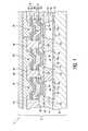
図1に示される電子装置1は、WO−A97/07550に記載されているものに類似の構成を有している。それは、各々が相変化材料を備えた複数のレジスタ36を備えた本体2を有し、相変化材料は第一の相と第二の相とを取りえるものである。示されていない他の実施形態では、本体2はレジスタ36を一つだけ備える。相変化材料はTe81Ge15S2As2である。他の実施形態では、それはTe81Ge15S2Sb2である。これとは別に、Te、Ge、Sb、そして、一つ又は複数の遷移金属TMを比率(TeaGebSb100−(a+b))cTM100−cで含み、ここで、下付き文字は原子パーセントであり、aは70パーセントより低く、bは5パーセントより高く且つ50パーセントより低く、そして、cは90から99.99パーセントの間である材料を相変化材料として用いてもよい。The electronic device 1 shown in FIG. 1 has a configuration similar to that described in WO-A97 / 07550. It has a body 2 with a plurality of resistors 36 each comprising a phase change material, the phase change material being capable of taking a first phase and a second phase. In other embodiments not shown, the body 2 comprises only one register 36. The phase change material is Te81 Ge15 S2 As2 . In other embodiments, it is Te81 Ge15 S2 Sb2 . Separately, Te, Ge, Sb and one or more transition metals TM are included in the ratio (Tea Geb Sb100- (a + b) )c TM100-c , where the subscript is Materials that are atomic percent, a is less than 70 percent, b is greater than 5 percent and less than 50 percent, and c is between 90 and 99.99 percent may be used as the phase change material.
レジスタ36の各々は本体2内に埋め込まれ、第一のコンタクト領域5と第二のコンタクト領域6とを備えた表面を有する。各レジスタ36は各々の第一のコンタクト領域5と第二のコンタクト領域6との間で電気的抵抗を有する。電気的抵抗は相変化材料が第一の相の場合に第一の値を有し、相変化材料が第二の相の場合に第二の値を有する。 Each of the resistors 36 is embedded in the body 2 and has a surface with a first contact region 5 and a second contact region 6. Each resistor 36 has an electrical resistance between the first contact region 5 and the second contact region 6. The electrical resistance has a first value when the phase change material is the first phase and has a second value when the phase change material is the second phase.
本体2は単結晶シリコン半導体ウエハ10を備え、これはp型にドープされた基板である。p−基板10内に形成されているのはn+チャネル12であり、これは、図1の平面に垂直な方向においてウエハ10を横切って延在しており、これは、一組の電極、この場合では、個々のメモリ素子30をアドレッシングするための選択線のx−yグリッドのy組を形成している。このn+グリッド構造の上部にあるのはnドープ結晶のエピタキシャル層14で、これは、例えば、約500nm厚みで、そこにpドープ分離チャネル16が形成されている。これらのpドープ分離チャネル16は図1に示されるように至る所でp−基板10へと延在している。それらはnエピタキシャル層14のアイランド18の周囲全面に延在し、これらアイランドは、このようにして、確定され、そして、互いに分離されている。これらアイランド18はWO−A97/07550の図2の上面図にさらに明確に示されており、そこでは、p−分離チャネルはn−エピタキシャル材料のアイランド18を確定し、そして、分離する分離グリッドを形成するものとして示されている。pドープ分離チャネルの代わりに誘電体材料を用いてアイランド18を分離してもよい。 The main body 2 comprises a single crystal silicon semiconductor wafer 10, which is a p-type doped substrate. Formed in the p-substrate 10 is an n +
誘電体材料の層20がアイランド18上部に穴部22を形成し、これら穴部22はp+材料の拡散領域24を確定している。p+領域とn−エピタキシャル層との結合が、層20の穴部22を介して露出するn−エピタキシャル層の各々の領域と直列になるp−n結合ダイオードを確定している。p−n結合ダイオードは選択装置26として機能する。A
選択装置26と個々に電気的に直列にコンタクトしているp+領域24の上部にメモリ素子30が堆積されている。メモリ素子30の各々は第一の導電体3を備え、これは第一のコンタクト領域5に電気的に接続され、そして、例えば、モリブデン等の耐食性が高く比較的薄い電気的コンタクト層32と、例えば、カーボン等の電気的に導電性の拡散バリア層34とを備えている。メモリ素子30の各々は、さらに、上記のように相変化材料で形成されたレジスタ36と第二の導電体4とを備え、第二の導電体4は第二のコンタクト領域6に電気的に接続され、そして、例えば、モリブデン等の耐食性の高い材料40の上部の薄い電気的コンタクト層と、例えば、カーボン等の電気的に導電性の拡散バリア層38とを備えている。コンタクト層32、34,38そして40、そして、レジスタ36はWO−A97/07550に記載されているものと同一である。 A
第一の導電体3と第二の導電体4とレジスタ36とは、上記詳細に説明されたように、相変化材料を加熱して第一の相から第二の相への転移が行われるように電流を流すことができる。 As described in detail above, the first conductor 3, the
メモリ素子30の横側周囲部分を取り囲む誘電体材料の層20及び39がメモリ素子30のレジスタ36を熱的に分離する。これは、さらに、加熱中に、レジスタと繋がっていない本体の他の部分への熱流を抑制、制限そして制御して、スイッチングエネルギを制限する。
この発明によれば、層20及び39の内の少なくとも一つが、サイズが0.5から50nmの間の孔を有する多孔性材料を備えた誘電体材料で成る。これらの孔はサイズが1から10nmの間であると好ましい。ある実施形態では、これらの孔は実質的に水分を含まない。少なくとも、レジスタ36と直接コンタクトがとられる層39はそのような材料で成ると好ましい。そのような多孔性材料の異なる実施形態を以下に記載する。 According to the invention, at least one of the
図1に示される電子装置を製造するに際し、層32,34,36,38そして40がエッチングされ、層39がそれらエッチングされた層の上部に形成され、続いて、エッチングされて、図に示されるように、メモリ素子30上部に開口が残される。層32,34,36,38そして40により形成される構造全体の上部に選択線42が堆積され、これらは、さらなる一組の電極、この場合では、個々のメモリ素子30をアドレッシングするための選択線のx−yグリッドのx組を形成する。選択線42は、例えば、アルミニウム、タングステン又は銅より形成されてもよい。完全な集積構造には、Si3N4又はプラスチック材料、例えば、ポリイミド等の適切なカプセルの材料のカプセル層44により覆われる。In manufacturing the electronic device shown in FIG. 1, layers 32, 34, 36, 38 and 40 are etched, and
このようにして、本体2はメモリ素子のアレイを備え、各メモリ素子はそれぞれメモリ素子30と選択装置26とを備える。本体2は、さらに、グリッド状の選択線12及び42を備え、選択装置26に接続された選択線12及び42を介して各メモリ素子が個別にアクセス可能となる。この集積回路の詳細はWO−A97/07550に記載されており、特に、図2乃至図4を参照されたい。 Thus, the main body 2 comprises an array of memory elements, each memory element comprising a
多孔性材料は、多孔性二酸化シリコン、又は、サイズが0.5から50nmの孔を有するチタン酸化物、バナジウム酸化物又はジルコニウム酸化物等を含む他の多孔性誘電体材料でもよい。これらの孔は実質的に水分を含まないと好ましい。この目的のために、多孔性二酸化シリコン、チタン酸化物、バナジウム酸化物又はジルコニウム酸化物は、例えば、加熱且つ又は真空処理されて、実質的に、存在するすべて水分が除去される。 The porous material may be porous silicon dioxide or other porous dielectric material including titanium oxide, vanadium oxide or zirconium oxide having pores with a size of 0.5 to 50 nm. These pores are preferably substantially free of moisture. For this purpose, the porous silicon dioxide, titanium oxide, vanadium oxide or zirconium oxide is, for example, heated and / or vacuum treated to remove substantially all the moisture present.
ある実施形態では孔が疎水性表面を有し、これは、この場合、水蒸気を含む雰囲気に電子装置を製造中に晒すことができるという利点がある。孔の疎水性表面は、例えば、Midland Michigan,USAのDow Chemicalにより販売されている多孔性SiLKTM等の疎水性の多孔性材料を用いることにより得られる。これとは別に、US−B1−6,352,945並びにUS−B1−6,383,955に記載されている材料を用いてもよい。In certain embodiments, the pores have a hydrophobic surface, which has the advantage that the electronic device can be exposed during manufacturing to an atmosphere containing water vapor. The hydrophobic surface of the pores can be obtained, for example, by using a hydrophobic porous material such as porous SiLK™ sold by Dow Chemical of Midland Michigan, USA. Apart from this, materials described in US-B1-6,352,945 and US-B1-6,383,955 may be used.
他の実施形態では多孔性材料は有機珪酸を含み、これはそれ自体は疎水性ではなく、アルキル基及びアリール基から選ばれた基を、それら基の少なくとも一部を有する表面のマトリクスとなるように組み込むことにより孔に疎水性表面が形成される。この実施形態では、多孔性材料はWO−A00/39028に記載されているように作られる。それは、テトラエトキシオルトシリケートとメチルトリメトキシシランとを0.85:0.15の比率で有する組成から得られる。 In other embodiments, the porous material comprises organosilicic acid, which is not itself hydrophobic, so that groups selected from alkyl and aryl groups become a matrix of the surface having at least a portion of those groups. Incorporating into the pores forms a hydrophobic surface in the pores. In this embodiment, the porous material is made as described in WO-A00 / 39028. It is obtained from a composition having tetraethoxyorthosilicate and methyltrimethoxysilane in a ratio of 0.85: 0.15.
他の実施形態では多孔性材料はテトラアルコキシシラン、ヒドロカルビルアルコキシシラン、表面活性剤、そして、溶剤を含む液層を基板に施し、テトラアルコキシシランとヒドロカルビルアルコキシシランとのモル比を多くても3:1とし、液層を加熱して表面活性剤及び溶剤を除去し、一方で、疎水性多孔層を形成する。 In another embodiment, the porous material is applied to the substrate with a liquid layer comprising tetraalkoxysilane, hydrocarbylalkoxysilane, surfactant, and solvent, and the molar ratio of tetraalkoxysilane to hydrocarbylalkoxysilane is at most 3: 1, the liquid layer is heated to remove the surfactant and solvent, while forming a hydrophobic porous layer.
この多孔層を得る方法は未公開の特許出願EP01,203,536.6に記載されている。この実施形態の電子装置1を製造するに際し、以下のようにして、層32,34,36,38そして40がエッチングされ、層39がそれらエッチングされた層の上部に形成される。層20,32,34,36,38そして40にテトラアルコキシシラン、ヒドロカルビルアルコキシシラン、表面活性剤、そして、溶剤の組成が与えられる。特定の組成が表1に掲げられており、それらの幾つかを以下に詳細に説明する。溶剤としては、アルコール、水、そして少量の酸の混合物が用いられる。適するアルコールは、とりわけ、メタノール、エタノール、プロパノール、そしてブタノールである。乾燥そして400°Cでの加熱の後に多孔性材料39が形成される。形成される層の厚みは、スピンコーティング中の回転数、組成の粘性、そして、組成の希釈度によることが分かっている。もし、セチルトリメチルアンモニウムブロミド(CTAB)が表面活性剤に用いられた場合は、孔のサイズは2から3nmで、もしプロニック(Pluronic)F127が表面活性剤に用いられた場合は、孔のサイズは7から8nmとなる。X線回折及びTEM装置による測定では孔のサイズはほぼ一定である。この層の特性は、表2に掲げられているような組成に依存する。 A method for obtaining this porous layer is described in the unpublished patent application EP01,203,536.6. In manufacturing the electronic device 1 of this embodiment, the
例1
テトラエトキシオルトシリケート(TEOS)、メチルトリメトキシシラン(MTMS)、水、そして、エタノールの組成物、これはHCLにより酸性にされるが、撹拌により形成される。TEOS:MTMS:H2O:エタノール:HCLのモル比は0.5:0.5:1:3:5.10−5である。この組成物は60°Cで90分間加熱された。水、エタノール、HCL、そして、セチルトリメチルアンモニウムブロミド(CTAB)がこの既に加熱された組成物に加えられてTEOS:MTMS:H2O:エタノール:HCL:CTABのモル比が0.5:0.5:7.5:20:0.006:0.10となる。この組成物は室温で三日間撹拌された。続いて、組成物がKarlSussCT62スピンコータ中で1000rpmで1分間スピンコーティングにより得られる。この層がホットプレート上で130°Cで10分間乾燥され、続いて、空気中で400°Cで1時間加熱される。このようにして、比誘電率が2.4、そして、表2に掲げられている多孔率が44%で厚みが200から400nmの多孔性層が得られる。Example 1
A composition of tetraethoxyorthosilicate (TEOS), methyltrimethoxysilane (MTMS), water, and ethanol, which is acidified by HCL but formed by stirring. TEOS:MTMS: H 2 O: ethanol molar ratio of HCL 0.5: 0.5: 1: 3: 5.10-5. The composition was heated at 60 ° C. for 90 minutes. Water, ethanol, HCL, and cetyltrimethylammonium bromide (CTAB) are added to the already heated composition to give a TEOS: MTMS: H2 O: ethanol: HCL: CTAB molar ratio of 0.5: 0. 5: 7.5: 20: 0.006: 0.10. The composition was stirred at room temperature for 3 days. Subsequently, the composition is obtained by spin coating in a KarlSuss CT62 spin coater at 1000 rpm for 1 minute. This layer is dried on a hot plate at 130 ° C. for 10 minutes, followed by heating in air at 400 ° C. for 1 hour. In this way, a porous layer having a relative dielectric constant of 2.4, a porosity of 44% and a thickness of 200 to 400 nm listed in Table 2 is obtained.
この場合では、誘電率は(MSIエレクトロニクスのHg−612型)水銀探針により周波数が1MHzにおいて測定される。多孔率は、層厚測定による屈折率、そして、ラザフォードバックスキャタリング(RBS)という当業者に知られている二つの方法の内の少なくとも一つにより測定される。屈折率は、JA Woolam Co.のVASEエリプソメータVB−250により測定される。この値から、偏光解消度が0.33のBruggemanの有効媒質近似により多孔率が測定される。 In this case, the dielectric constant (MSI Electronics Hg-612 type) is measured with a mercury probe at a frequency of 1 MHz. Porosity is measured by at least one of two methods known to those skilled in the art: refractive index from layer thickness measurements and Rutherford Backscattering (RBS). The refractive index is measured by JA Woolam Co. VASE ellipsometer VB-250. From this value, the porosity is measured by Bruggeman's effective medium approximation with a depolarization degree of 0.33.
例2
TEOS、MTMS、水、エタノール、HCL、そして、CTBAの組成物が用意され、
表面活性剤の量が例1に比べて0.22に増やされる。この実施形態では表面活性剤は陽イオンの表面活性剤で、表面活性剤とアルコキシシラン全体とが0.1:1より大きいモル比で存在する。組成物は例1で記載されたように処理される。これにより、多孔率が45パーセントを越える、56%の多孔性材料の電子装置1が得られる。Example 2
TEOS, MTMS, water, ethanol, HCL, and CTBA compositions are prepared,
The amount of surfactant is increased to 0.22 compared to Example 1. In this embodiment, the surfactant is a cationic surfactant and the surfactant and the entire alkoxysilane are present in a molar ratio greater than 0.1: 1. The composition is processed as described in Example 1. As a result, an electronic device 1 made of a porous material having a porosity of more than 45% and having a porosity of 56% is obtained.
例3
例2の組成物は室温で三日間撹拌される。続いて、組成物はKarlSussCT62スピンコータ中で1000rpmで1分間スピンコーティングにより得られる。層が130°Cで10分間乾燥され、続いて、93vol.%N2及び7vol.%H2を備えるガス内で400°Cで1時間加熱される。
TEOS = テトラエトキシオルトシリケート
HCAS = ヒドロカルビルアルコキシシラン
CTAB = セチルトリメチルアンモニウムブロミド
MTMS = メチルトリメトキシルシラン
phTES = フェニルトリエトキシシラン
F127 = プルロニックF127、ポリエチレン酸化物と、ポリプロピレン酸化物と、そして、ポリエチレン酸化物とをブロックとして備えるトリブロックポリマー
Brij76 = ポリオキシエチレン(10)ステアリルエーテル、C18H37(OCH2CH2)nOH、n ≒ 10
DMDES =ヂメチルジエトキシシランExample 3
The composition of Example 2 is stirred at room temperature for 3 days. Subsequently, the composition is obtained by spin coating in a KarlSuss CT62 spin coater at 1000 rpm for 1 minute. The layer was dried at 130 ° C. for 10 minutes, followed by 93 vol. %N 2 and 7vol. Heat in a gas with% H2 at 400 ° C. for 1 hour.
TEOS = tetraethoxyorthosilicate HCAS = hydrocarbylalkoxysilane CTAB = cetyltrimethylammonium bromide MTMS = methyltrimethoxylsilane phTES = phenyltriethoxysilane F127 = pluronic F127, polyethylene oxide, polypropylene oxide, and polyethylene oxide Is a triblock polymer Brij76 = polyoxyethylene (10) stearyl ether, C18 H37 (OCH2 CH2 )n OH, n≈10
DMDES = dimethyldiethoxysilane

WO−A00/57,498により知られているものと類似の、図2に示される、電子装置100の他の実施形態では、電子装置100が、例えば、図示された構造の他の半導体素子の堆積のためのp基板を形成するpドープシリコンである半導体基板102上に形成される。これとは別に、基板は単結晶GaAsウエハ又はガラス基板でもよい。それは、WO−A00/57,498により知られるもとの同一のメモリセルのNxMアレイであり、特に、この特許出願の図4を参照されたい。ここで、NとMとは整数である。各メモリセルはそれぞれメモリ素子103と選択装置104とを備える。図2に示される実施形態では、各メモリセルは二つの独立したメモリ素子103Aと103Bとを備える。第一の導電体130Aと、第二の導電体270Aと、レジスタ250と、そして、誘電体材料の層126,140、そして、260とがメモリ素子103Aを構成し、第一の導電体130Bと、第二の導電体270Bと、レジスタ250と、そして、層126,140、そして、260とがメモリ素子103Bを構成する。即ち、メモリ素子103Aと103Bとが同じレジスタ250並びに同じ層126,140、そして、260を共有する。 In another embodiment of the
上記のように相変化材料を備えることができるレジスタ250は第一のコンタクト領域132A、132Bと第二のコンタクト領域272A、272Bとを備えた表面を有する。メモリ素子103Aの一部として、レジスタ250は、第一のコンタクト領域132Aと第二のコンタクト領域272Aとの間に、相変化材料が第一の相では第一の値、相変化材料が第二の相では第二の値となる電気抵抗を有する。メモリ素子103Bの一部として、レジスタ250は、第一のコンタクト領域132Bと第二のコンタクト領域272Bとの間に、相変化材料が第一の相では第一の値、相変化材料が第二の相では第二の値となる電気抵抗を有する。第一の導電体130A及び130Bは、例えば、上記の第一の導電体3と同じ材料を備えてもよく、それぞれ第一のコンタクト領域132A及び132Bに電気的に接続される。第二の導電体270A及び270Bは、例えば、上記の第二の導電体4と同じ材料を備えてもよく、それぞれ第二のコンタクト領域272A及び272Bに電気的に接続される。第一の導電体130Aと、第二の導電体270Aと、そして、レジスタ250とは相変化材料を加熱して第一の相から第二の相への転移が行われるように電流を流すことができ、第一のメモリ素子103Aの電気抵抗を変えることができる。同様に、第一の導電体130B、第二の導電体270B、そして、レジスタ250は相変化材料を加熱して第一の相から第二の相への転移が行われるように電流を流すことができ、第二のメモリ素子103Bの電気抵抗を変えることができる。
図2に示される実施形態では、第二の導電体270A及び270Bを介してのみレジスタ250が出力線271に接続されるように、誘電体材料の層260により、レジスタ250と出力線271との間が電気的に分離されている。誘電体材料層260は、さらに、加熱中に、レジスタ250と繋がっていない本体101の他の部分への熱流を低減するサーマルブランケットとなる。誘電体層140は第一の導電体130Bから第一の導電体130Aを電気的に分離する。ボロフォスフォスシリケート(BPSG)を備えることができる誘電体層180が電子装置100上部に堆積される。 In the embodiment shown in FIG. 2, the layer of
WO−A00/57,498により知られている電子装置と同様に、第一の導電体130A及び130Bは導電横壁スペーサであり、これは、導電スペーサとも呼ばれ、誘電体領域126の横壁表面126Sに沿って形成される。レジスタ250と第一の導電体130A、130Bとの間のコンタクト領域が、それぞれ、第一のコンタクト領域132A、132Bである。そこで、レジスタ250と第一の導電体130A及び130Bとの間の電気的結合のみが、第一のコンタクト領域132A及び132Bの全体又は一部を介してもたらされる。第一の導電体130A及び130Bの残部は誘電体層126及び140によりレジスタ250から電気的に分離される。 Similar to the electronic device known from WO-A00 / 57,498, the
これとは別に、第一の導電体130A及び又は130Bは、WO−A00/57,498により知られているように、バイアホールの横壁の表面又は複数の表面上に一つ又は複数のコンタクト層を一様に堆積することにより、導電横壁スペーサとして形成されてもよい。このバイアホールは円形、正方形、長方形、又は、不規則な形状であってもよい。さらに、導電横壁スペーサは、ピラー又はメサの横壁表面上に一つ又は複数のコンタクト層を一様に堆積することにより形成されてもよい。バイア内の残部スペースには、好ましくは、水分を含まない孔の多孔性材料を備えた誘電体材料の層で満たされる。この材料の実施形態は上記されたものである。 Alternatively, the
この発明によれば、層126,140,180、そして、260の内の少なくとも一層が、サイズが0.5から50nmの間の孔を有する多孔性材料を備える誘電体材料より成る。このようにして、レジスタ250とは繋がっていない本体101の部分への熱流が低減され、その結果、スイッチングパワーが低減される。レジスタ250と直接コンタクトがとられる層126,140,そして、260の内の一つはそのような材料から成ると好ましい。孔のサイズは1から10nmの間であると好ましい。好ましい実施形態では、孔は実質的に水分を含まない。多孔性材料の異なる実施形態は上記されたものである。 According to the invention, at least one of the
図2に示される実施形態では、第一のコンタクト領域132A及び132Bが、それぞれ、対応する第二のコンタクト領域272A及び272Bより小さい。第一の導電体130A及び130Bは、それぞれ、第一のコンタクト領域132A及び132Bとコンタクトがとられる部分を備える。この部分は、実質的に水分を含まない多孔性材料を備える層126及び140に埋め込まれると好ましく、何故ならば、この場合、レジスタ250とは繋がらない本体101の部分への熱流が、特に、効果的に低減されるからである。第一のコンタクト領域132A及び132Bが比較的小さいので、第一の導電体130A及び130Bの部分内の電流密度が特に大きくなり、レジスタ250近傍でのジュール熱が増加する。相転移を可能にするこの熱効果は、改善された熱的分離のために特に大きい。In the embodiment shown in FIG. 2, the
本体101は、各選択装置104に接続された各選択線120及び190を介して各メモリ素子が個々にアクセス可能なように、N本の第一の選択線190と、M本の第二の選択線120と、一本の出力線271とを備える選択線グリッドを備える。電子装置100のメモリ素子103A及び103Bの各々は、MOSFET、さらに、特に、NMOSトランジスタである、選択装置104に電気的に接続されている。MOSFETはnドープソース領域110と,nドープドレイン領域112と、そして、ゲート領域118とを備える。ソース領域110及びドレイン領域112は二つ以上のnドープ材料、即ち、軽くドープされたn部分とさらに重くドープされたn+部分とを備えてもよい。 The
nドープのソース領域110とドレイン領域112とはチャネル領域114により分離されている。チャネル領域114上部に形成されたゲート領域118が、チャネル領域114を介してソース領域110からドレイン領域112に流れる電流を制御する。ゲート領域118はポリシリコンの層を備えると好ましい。誘電体領域116により、ゲート領域118がチャネル領域114から分離されている。 The n-doped
チャネルストップ領域113がnドープドレイン領域112内に形成され、NMOSトランジスタを分離するために、二つの隣り合い且つ電気的に分離されているドレイン領域112を形成している。通常、チャネルストップ領域113はソース領域110及びドレイン領域112とは反対の導電型である。図に示されるNMOSの実施形態では、チャネルストップ領域113はpドープシリコンを備える。 A
ゲート領域上に選択線120が形成され、これら選択線はタングステンシリサイドの層を備える好ましい。選択線120は電気信号をゲート領域118に分配するのに用いられる。誘電体領域122が選択線120上に形成され、これら誘電体領域は実質的に水分を含まない孔を有する多孔性材料を備えると好ましい。誘電体領域122は選択線120を電子装置100の近隣領域から電気的に分離する。層116,118,そして、120の積層が全体としてゲートスタックと呼ばれる。誘電体領域126がゲートスタックの横壁表面上に形成されている。
選択線190が上部分離領域180の上部に形成されている。選択線190は、アルミニウム又は銅等の導電材料から形成されてもよい。タングステンプラグ144が選択線190をソ−ス領域110に接続している。図2に示される特別な実施形態では、二つのNMOSトランジスタがタングステンプラグ144の各々を共有していることに注意されたい。チタンシリサイド(示されていない)の層がシリコン基板表面に形成されて、基板102と導電横壁スペーサ130A及び130Bとの間、並びに、基板102と導電プラグ144との間の導電性を高めてもよい。導電プラグ144は、誘電体層126により、ゲートスタックから電気的に分離される。 A
メモリ素子103A及び103Bの第一の導電体130A及び130Bは、それぞれ、金属酸化半導体電界効果型トランジスタのソース領域110とドレイン領域112とから選択された第一の領域に電気的に接続される。図2の実施形態では、第一の領域はドレイン領域112である。メモリ素子103A及び103Bの各々の第二の導電体270が出力線271に接続され、これは、例えば、第二の導電体270と同じ材料を備えてもよい。ソース領域110とドレイン領域112とから選択され、第一の領域とは繋がっていない金属酸化半導体電界効果型トランジスタの第二の領域がN本の第一の選択線190の内の一本に電気的に接続される。ゲート領域118はM本の第二の選択線120の内の一本に電気的に接続される。 The
要約すると、電子装置1,100は、第一の相と第二の相とを取りえる相変化材料を備えたレジスタ36,250を備える。レジスタ36,250は、相変化材料が第一の相の場合に第一の値となり、相変化材料が第二の相の場合に第二の値となる電気的抵抗を有する。レジスタ36,250は、第一の導電体3,130A,130B、そして、第二の導電体4,270に電気的に接続され、これらは、相変化材料を加熱して第一の相から第二の相への転移が行われるように電流を流すことができる。電子装置1,100は、さらに、加熱中にレジスタ36,250と繋がっていない本体2,101の部分への熱流を低減されるための誘電体材料の層20,39,126,140,260を備え、この発明の誘電体材料はサイズが0.5から50nmの間の孔を有する多孔性材料を備える。 In summary, the
上記の各実施形態はこの発明を限定するものではなく、当業者であれば添付請求項の範囲から外れることなく多くの代替え実施形態を考案することができることに留意されたい。文言「備える」は請求項に掲げられた要素又は工程以外の存在を排除するものではない。 It should be noted that the above embodiments are not intended to limit the present invention and that many alternative embodiments can be devised by those skilled in the art without departing from the scope of the appended claims. The word “comprising” does not exclude the presence of elements or steps other than those listed in a claim.
Claims (12)
Translated fromJapanese第一の相と第二の相とを取りえる相変化材料を備え、第一のコンタクト領域と第二のコンタクト領域とを備えた表面を有し、前記第一のコンタクト領域と前記第二のコンタクト領域との間で電気的抵抗を有し、該電気的抵抗は前記相変化材料が前記第一の相の場合に第一の値を有し、前記相変化材料が前記第二の相の場合に第二の値を有するレジスタと、
前記第一のコンタクト領域に電気的に接続された第一の導電体と、
前記第二のコンタクト領域に電気的に接続された第二の導電体とを備え、
前記第一の導電体と前記第二の導電体と前記レジスタとは前記相変化材料を加熱して前記第一の相から前記第二の相への転移が行われるように電流を流すことができ、
前記電子装置は、さらに、
前記加熱の間に前記本体のその他の部分への熱流を低減させ、サイズが0.5から50nmの間の複数の孔を有する多孔性材料を備えた誘電体材料の層を備えたことを特徴とする電子装置。An electronic device having a body,
A phase change material capable of taking a first phase and a second phase, and having a surface with a first contact region and a second contact region, the first contact region and the second phase An electrical resistance to the contact region, the electrical resistance having a first value when the phase change material is the first phase, and the phase change material being of the second phase. A register having a second value in the case;
A first conductor electrically connected to the first contact region;
A second conductor electrically connected to the second contact region,
The first conductor, the second conductor, and the resistor may heat the phase change material to pass a current so that the transition from the first phase to the second phase occurs. Can
The electronic device further includes:
Comprising a layer of dielectric material comprising a porous material having a plurality of pores with a size between 0.5 and 50 nm, reducing heat flow to the rest of the body during the heating; An electronic device.
前記液層を加熱して、前記表面活性剤と前記溶剤とを除去し、そして、前記疎水性多孔性層を形成することにより前記疎水性多孔性層が得られることを特徴とする請求項5に記載の電子装置。A liquid layer comprising a tetraalkoxysilane, a hydrocarbylalkoxysilane, a surfactant, and a solvent is applied to the substrate, the molar ratio between the tetraalkoxylsilane and the hydrocarbylalkosylsilane being at most 3: 1;
6. The hydrophobic porous layer is obtained by heating the liquid layer to remove the surfactant and the solvent, and forming the hydrophobic porous layer. An electronic device according to 1.
各々がメモリ素子と選択装置とを備えた複数のメモリセルのアレイと、
複数の選択線のグリッドとを備え、
各メモリセルは、前記選択装置と接続された複数の選択線を介して個々にアクセス可能であることを特徴とする請求項1に記載の電子装置。The first conductor, the second conductor, the resistor, and the layer constitute a memory element, and the main body includes:
An array of a plurality of memory cells each comprising a memory element and a selection device;
With a grid of multiple selection lines,
The electronic device according to claim 1, wherein each memory cell is individually accessible through a plurality of selection lines connected to the selection device.
前記複数の選択線のグリッドはN本の第一の選択線と、M本の第二の選択線と、ここで、N及びMは整数であり、そして、一本の出力線とを備え、
各メモリ素子の前記第一の導電体は前記金属酸化半導体電界効果型トランジスタの前記ソース領域と前記ドレイン領域とから選択された第一の領域に電気的に接続され、各メモリ素子の前記第二の導電体は前記出力線に電気的に接続され、前記ソース領域と前記ドレイン領域とから選択され、そして、前記第一の領域とは繋がらない、前記金属酸化半導体電界効果型トランジスタの第二の領域が前記N本の第一の選択線の内の一本に電気的に接続され、前記ゲート領域が前記M本の第二の選択線の内の一本に電気的に接続されていることを特徴とする請求項1に記載の電子装置。The selection device includes a metal oxide semiconductor field effect transistor having a source region 110, a drain region 112, and a gate region,
The grid of selection lines includes N first selection lines, M second selection lines, where N and M are integers, and a single output line,
The first conductor of each memory element is electrically connected to a first region selected from the source region and the drain region of the metal oxide semiconductor field effect transistor, and the second conductor of each memory element is A conductor of the metal oxide semiconductor field effect transistor is electrically connected to the output line, selected from the source region and the drain region, and not connected to the first region. The region is electrically connected to one of the N first selection lines, and the gate region is electrically connected to one of the M second selection lines. The electronic device according to claim 1.
Applications Claiming Priority (2)
| Application Number | Priority Date | Filing Date | Title |
|---|---|---|---|
| EP02079220 | 2002-10-11 | ||
| PCT/IB2003/003865WO2004034482A2 (en) | 2002-10-11 | 2003-08-25 | Electric device comprising phase change material |
Publications (1)
| Publication Number | Publication Date |
|---|---|
| JP2006502578Atrue JP2006502578A (en) | 2006-01-19 |
Family
ID=32088028
Family Applications (1)
| Application Number | Title | Priority Date | Filing Date |
|---|---|---|---|
| JP2004542691AWithdrawnJP2006502578A (en) | 2002-10-11 | 2003-08-25 | Electronic device with phase change material |
Country Status (10)
| Country | Link |
|---|---|
| US (1) | US20060163554A1 (en) |
| EP (1) | EP1554763B1 (en) |
| JP (1) | JP2006502578A (en) |
| KR (1) | KR20050053750A (en) |
| CN (1) | CN100521276C (en) |
| AT (1) | ATE335289T1 (en) |
| AU (1) | AU2003259447A1 (en) |
| DE (1) | DE60307306T2 (en) |
| TW (1) | TWI311825B (en) |
| WO (1) | WO2004034482A2 (en) |
Cited By (10)
| Publication number | Priority date | Publication date | Assignee | Title |
|---|---|---|---|---|
| JP2007194426A (en)* | 2006-01-19 | 2007-08-02 | Toshiba Corp | Semiconductor memory device |
| WO2007099595A1 (en)* | 2006-02-28 | 2007-09-07 | Renesas Technology Corp. | Semiconductor device and process for producing the same |
| JP2007243169A (en)* | 2006-02-07 | 2007-09-20 | Qimonda Ag | Phase change memory cell with thermal barrier |
| JP2007281283A (en)* | 2006-04-10 | 2007-10-25 | Kobe Steel Ltd | Method for manufacturing porous film, and porous film manufactured by same |
| JP2008078625A (en)* | 2006-07-20 | 2008-04-03 | Qimonda North America Corp | Phase change memory cell with nanocomposite insulator |
| JP2008103676A (en)* | 2006-07-18 | 2008-05-01 | Qimonda North America Corp | Phase variation memory having stepwise programming characteristics |
| JP2008172236A (en)* | 2007-01-08 | 2008-07-24 | Samsung Electronics Co Ltd | Memory device including thermal conductor located between program volumes |
| JP2011510496A (en)* | 2008-01-16 | 2011-03-31 | エヌエックスピー ビー ヴィ | Multilayer structure having phase change material layer and method of manufacturing the same |
| JP2012108320A (en)* | 2010-11-17 | 2012-06-07 | Canon Inc | Antireflection film and manufacturing method thereof |
| JP2024510884A (en)* | 2021-03-23 | 2024-03-12 | インターナショナル・ビジネス・マシーンズ・コーポレーション | phase change memory |
Families Citing this family (82)
| Publication number | Priority date | Publication date | Assignee | Title |
|---|---|---|---|---|
| US7709334B2 (en) | 2005-12-09 | 2010-05-04 | Macronix International Co., Ltd. | Stacked non-volatile memory device and methods for fabricating the same |
| KR101100422B1 (en)* | 2005-01-27 | 2011-12-30 | 삼성전자주식회사 | Resistive DRAM device and its operation method |
| US7361925B2 (en)* | 2005-02-10 | 2008-04-22 | Infineon Technologies Ag | Integrated circuit having a memory including a low-k dielectric material for thermal isolation |
| US7348590B2 (en)* | 2005-02-10 | 2008-03-25 | Infineon Technologies Ag | Phase change memory cell with high read margin at low power operation |
| DE102005014645B4 (en) | 2005-03-31 | 2007-07-26 | Infineon Technologies Ag | Connection electrode for phase change material, associated phase change memory element and associated manufacturing method |
| KR100707190B1 (en) | 2005-05-07 | 2007-04-13 | 삼성전자주식회사 | Phase change memory device including nanowires and method for manufacturing same |
| US7635855B2 (en) | 2005-11-15 | 2009-12-22 | Macronix International Co., Ltd. | I-shaped phase change memory cell |
| US7786460B2 (en) | 2005-11-15 | 2010-08-31 | Macronix International Co., Ltd. | Phase change memory device and manufacturing method |
| US7449710B2 (en) | 2005-11-21 | 2008-11-11 | Macronix International Co., Ltd. | Vacuum jacket for phase change memory element |
| US7599217B2 (en) | 2005-11-22 | 2009-10-06 | Macronix International Co., Ltd. | Memory cell device and manufacturing method |
| US7459717B2 (en) | 2005-11-28 | 2008-12-02 | Macronix International Co., Ltd. | Phase change memory cell and manufacturing method |
| US7688619B2 (en)* | 2005-11-28 | 2010-03-30 | Macronix International Co., Ltd. | Phase change memory cell and manufacturing method |
| US7531825B2 (en) | 2005-12-27 | 2009-05-12 | Macronix International Co., Ltd. | Method for forming self-aligned thermal isolation cell for a variable resistance memory array |
| US8062833B2 (en) | 2005-12-30 | 2011-11-22 | Macronix International Co., Ltd. | Chalcogenide layer etching method |
| US7741636B2 (en) | 2006-01-09 | 2010-06-22 | Macronix International Co., Ltd. | Programmable resistive RAM and manufacturing method |
| US7560337B2 (en) | 2006-01-09 | 2009-07-14 | Macronix International Co., Ltd. | Programmable resistive RAM and manufacturing method |
| EP2005494B1 (en) | 2006-03-24 | 2012-09-12 | Nxp B.V. | Electric device with phase change resistor |
| US7608848B2 (en)* | 2006-05-09 | 2009-10-27 | Macronix International Co., Ltd. | Bridge resistance random access memory device with a singular contact structure |
| JP4865433B2 (en)* | 2006-07-12 | 2012-02-01 | ルネサスエレクトロニクス株式会社 | Semiconductor device and manufacturing method thereof |
| US7785920B2 (en) | 2006-07-12 | 2010-08-31 | Macronix International Co., Ltd. | Method for making a pillar-type phase change memory element |
| US7504653B2 (en) | 2006-10-04 | 2009-03-17 | Macronix International Co., Ltd. | Memory cell device with circumferentially-extending memory element |
| US20080089642A1 (en)* | 2006-10-12 | 2008-04-17 | Annette Claire Grot | Photonic crystal sensor for small volume sensing |
| US7863655B2 (en) | 2006-10-24 | 2011-01-04 | Macronix International Co., Ltd. | Phase change memory cells with dual access devices |
| US7476587B2 (en) | 2006-12-06 | 2009-01-13 | Macronix International Co., Ltd. | Method for making a self-converged memory material element for memory cell |
| US7903447B2 (en) | 2006-12-13 | 2011-03-08 | Macronix International Co., Ltd. | Method, apparatus and computer program product for read before programming process on programmable resistive memory cell |
| US7718989B2 (en) | 2006-12-28 | 2010-05-18 | Macronix International Co., Ltd. | Resistor random access memory cell device |
| US7619237B2 (en)* | 2007-02-21 | 2009-11-17 | Macronix International Co., Ltd. | Programmable resistive memory cell with self-forming gap |
| US7956344B2 (en) | 2007-02-27 | 2011-06-07 | Macronix International Co., Ltd. | Memory cell with memory element contacting ring-shaped upper end of bottom electrode |
| US7786461B2 (en) | 2007-04-03 | 2010-08-31 | Macronix International Co., Ltd. | Memory structure with reduced-size memory element between memory material portions |
| US7569844B2 (en)* | 2007-04-17 | 2009-08-04 | Macronix International Co., Ltd. | Memory cell sidewall contacting side electrode |
| US7729161B2 (en) | 2007-08-02 | 2010-06-01 | Macronix International Co., Ltd. | Phase change memory with dual word lines and source lines and method of operating same |
| US7919766B2 (en) | 2007-10-22 | 2011-04-05 | Macronix International Co., Ltd. | Method for making self aligning pillar memory cell device |
| KR20090097362A (en)* | 2008-03-11 | 2009-09-16 | 삼성전자주식회사 | Resistor Memory Device and Formation Method |
| US8030634B2 (en)* | 2008-03-31 | 2011-10-04 | Macronix International Co., Ltd. | Memory array with diode driver and method for fabricating the same |
| US7825398B2 (en) | 2008-04-07 | 2010-11-02 | Macronix International Co., Ltd. | Memory cell having improved mechanical stability |
| US7791057B2 (en) | 2008-04-22 | 2010-09-07 | Macronix International Co., Ltd. | Memory cell having a buried phase change region and method for fabricating the same |
| US8077505B2 (en) | 2008-05-07 | 2011-12-13 | Macronix International Co., Ltd. | Bipolar switching of phase change device |
| US7701750B2 (en) | 2008-05-08 | 2010-04-20 | Macronix International Co., Ltd. | Phase change device having two or more substantial amorphous regions in high resistance state |
| US8415651B2 (en) | 2008-06-12 | 2013-04-09 | Macronix International Co., Ltd. | Phase change memory cell having top and bottom sidewall contacts |
| US8586960B2 (en)* | 2008-06-19 | 2013-11-19 | International Business Machines Corporation | Integrated circuit including vertical diode |
| US8134857B2 (en) | 2008-06-27 | 2012-03-13 | Macronix International Co., Ltd. | Methods for high speed reading operation of phase change memory and device employing same |
| KR100962019B1 (en)* | 2008-06-30 | 2010-06-08 | 주식회사 하이닉스반도체 | Phase change memory device comprising a protective film and method of manufacturing the same |
| US7932506B2 (en) | 2008-07-22 | 2011-04-26 | Macronix International Co., Ltd. | Fully self-aligned pore-type memory cell having diode access device |
| US7903457B2 (en) | 2008-08-19 | 2011-03-08 | Macronix International Co., Ltd. | Multiple phase change materials in an integrated circuit for system on a chip application |
| US7719913B2 (en) | 2008-09-12 | 2010-05-18 | Macronix International Co., Ltd. | Sensing circuit for PCRAM applications |
| IT1391864B1 (en)* | 2008-09-30 | 2012-01-27 | St Microelectronics Rousset | RESISTIVE MEMORY CELL AND METHOD FOR THE MANUFACTURE OF A RESISTIVE MEMORY CELL |
| US8324605B2 (en) | 2008-10-02 | 2012-12-04 | Macronix International Co., Ltd. | Dielectric mesh isolated phase change structure for phase change memory |
| US7897954B2 (en) | 2008-10-10 | 2011-03-01 | Macronix International Co., Ltd. | Dielectric-sandwiched pillar memory device |
| US8036014B2 (en) | 2008-11-06 | 2011-10-11 | Macronix International Co., Ltd. | Phase change memory program method without over-reset |
| US7869270B2 (en) | 2008-12-29 | 2011-01-11 | Macronix International Co., Ltd. | Set algorithm for phase change memory cell |
| US8089137B2 (en) | 2009-01-07 | 2012-01-03 | Macronix International Co., Ltd. | Integrated circuit memory with single crystal silicon on silicide driver and manufacturing method |
| US8107283B2 (en) | 2009-01-12 | 2012-01-31 | Macronix International Co., Ltd. | Method for setting PCRAM devices |
| US8030635B2 (en) | 2009-01-13 | 2011-10-04 | Macronix International Co., Ltd. | Polysilicon plug bipolar transistor for phase change memory |
| US8064247B2 (en) | 2009-01-14 | 2011-11-22 | Macronix International Co., Ltd. | Rewritable memory device based on segregation/re-absorption |
| US8933536B2 (en) | 2009-01-22 | 2015-01-13 | Macronix International Co., Ltd. | Polysilicon pillar bipolar transistor with self-aligned memory element |
| US8084760B2 (en)* | 2009-04-20 | 2011-12-27 | Macronix International Co., Ltd. | Ring-shaped electrode and manufacturing method for same |
| US8173987B2 (en) | 2009-04-27 | 2012-05-08 | Macronix International Co., Ltd. | Integrated circuit 3D phase change memory array and manufacturing method |
| US8097871B2 (en) | 2009-04-30 | 2012-01-17 | Macronix International Co., Ltd. | Low operational current phase change memory structures |
| US7933139B2 (en) | 2009-05-15 | 2011-04-26 | Macronix International Co., Ltd. | One-transistor, one-resistor, one-capacitor phase change memory |
| US8350316B2 (en)* | 2009-05-22 | 2013-01-08 | Macronix International Co., Ltd. | Phase change memory cells having vertical channel access transistor and memory plane |
| US7968876B2 (en) | 2009-05-22 | 2011-06-28 | Macronix International Co., Ltd. | Phase change memory cell having vertical channel access transistor |
| US8809829B2 (en) | 2009-06-15 | 2014-08-19 | Macronix International Co., Ltd. | Phase change memory having stabilized microstructure and manufacturing method |
| US8406033B2 (en) | 2009-06-22 | 2013-03-26 | Macronix International Co., Ltd. | Memory device and method for sensing and fixing margin cells |
| US8363463B2 (en) | 2009-06-25 | 2013-01-29 | Macronix International Co., Ltd. | Phase change memory having one or more non-constant doping profiles |
| US8238149B2 (en) | 2009-06-25 | 2012-08-07 | Macronix International Co., Ltd. | Methods and apparatus for reducing defect bits in phase change memory |
| US8198619B2 (en) | 2009-07-15 | 2012-06-12 | Macronix International Co., Ltd. | Phase change memory cell structure |
| US8110822B2 (en) | 2009-07-15 | 2012-02-07 | Macronix International Co., Ltd. | Thermal protect PCRAM structure and methods for making |
| US7894254B2 (en) | 2009-07-15 | 2011-02-22 | Macronix International Co., Ltd. | Refresh circuitry for phase change memory |
| US8064248B2 (en) | 2009-09-17 | 2011-11-22 | Macronix International Co., Ltd. | 2T2R-1T1R mix mode phase change memory array |
| US8178387B2 (en) | 2009-10-23 | 2012-05-15 | Macronix International Co., Ltd. | Methods for reducing recrystallization time for a phase change material |
| US8729521B2 (en) | 2010-05-12 | 2014-05-20 | Macronix International Co., Ltd. | Self aligned fin-type programmable memory cell |
| US8310864B2 (en) | 2010-06-15 | 2012-11-13 | Macronix International Co., Ltd. | Self-aligned bit line under word line memory array |
| US8395935B2 (en) | 2010-10-06 | 2013-03-12 | Macronix International Co., Ltd. | Cross-point self-aligned reduced cell size phase change memory |
| US8497705B2 (en) | 2010-11-09 | 2013-07-30 | Macronix International Co., Ltd. | Phase change device for interconnection of programmable logic device |
| US8467238B2 (en) | 2010-11-15 | 2013-06-18 | Macronix International Co., Ltd. | Dynamic pulse operation for phase change memory |
| KR101199262B1 (en)* | 2011-03-21 | 2012-11-12 | 한국과학기술연구원 | Resistance switchable conductive filler for ReRAM and its preparation method |
| US9559113B2 (en) | 2014-05-01 | 2017-01-31 | Macronix International Co., Ltd. | SSL/GSL gate oxide in 3D vertical channel NAND |
| US9672906B2 (en) | 2015-06-19 | 2017-06-06 | Macronix International Co., Ltd. | Phase change memory with inter-granular switching |
| US10483322B2 (en)* | 2017-06-08 | 2019-11-19 | Taiwan Semiconductor Manufacturing Co., Ltd. | Memory device and method for fabricating the same |
| US10147876B1 (en)* | 2017-08-31 | 2018-12-04 | Sandisk Technologies Llc | Phase change memory electrode with multiple thermal interfaces |
| CN112133825A (en)* | 2020-09-03 | 2020-12-25 | 中国科学院上海微系统与信息技术研究所 | High-stability phase change storage unit and preparation method thereof |
| US11980110B2 (en)* | 2021-09-20 | 2024-05-07 | International Business Machines Corporation | Insulated phase change memory using porous dielectrics |
Family Cites Families (9)
| Publication number | Priority date | Publication date | Assignee | Title |
|---|---|---|---|---|
| US6087674A (en)* | 1996-10-28 | 2000-07-11 | Energy Conversion Devices, Inc. | Memory element with memory material comprising phase-change material and dielectric material |
| US5825046A (en)* | 1996-10-28 | 1998-10-20 | Energy Conversion Devices, Inc. | Composite memory material comprising a mixture of phase-change memory material and dielectric material |
| US6141241A (en)* | 1998-06-23 | 2000-10-31 | Energy Conversion Devices, Inc. | Universal memory element with systems employing same and apparatus and method for reading, writing and programming same |
| ATE363455T1 (en)* | 1998-12-23 | 2007-06-15 | Battelle Memorial Institute | MESOPOROUS SILICON DIOXIDE FILM BASED ON A SOLUTION CONTAINING SURFACTANT AND METHOD FOR THE PRODUCTION THEREOF |
| JP2004504716A (en)* | 2000-07-13 | 2004-02-12 | ザ リージェンツ オブ ザ ユニバーシティ オブ カリフォルニア | Silica zeolite low dielectric constant thin film |
| US6339544B1 (en)* | 2000-09-29 | 2002-01-15 | Intel Corporation | Method to enhance performance of thermal resistor device |
| US6670285B2 (en)* | 2001-03-14 | 2003-12-30 | International Business Machines Corporation | Nitrogen-containing polymers as porogens in the preparation of highly porous, low dielectric constant materials |
| EP1318552A1 (en)* | 2001-12-05 | 2003-06-11 | STMicroelectronics S.r.l. | Small area contact region, high efficiency phase change memory cell and fabrication method thereof |
| JP3948292B2 (en)* | 2002-02-01 | 2007-07-25 | 株式会社日立製作所 | Semiconductor memory device and manufacturing method thereof |
- 2003
- 2003-08-25JPJP2004542691Apatent/JP2006502578A/ennot_activeWithdrawn
- 2003-08-25KRKR1020057006241Apatent/KR20050053750A/ennot_activeAbandoned
- 2003-08-25DEDE60307306Tpatent/DE60307306T2/ennot_activeExpired - Lifetime
- 2003-08-25AUAU2003259447Apatent/AU2003259447A1/ennot_activeAbandoned
- 2003-08-25ATAT03807898Tpatent/ATE335289T1/ennot_activeIP Right Cessation
- 2003-08-25USUS10/530,449patent/US20060163554A1/ennot_activeAbandoned
- 2003-08-25CNCNB038239639Apatent/CN100521276C/ennot_activeExpired - Fee Related
- 2003-08-25EPEP03807898Apatent/EP1554763B1/ennot_activeExpired - Lifetime
- 2003-08-25WOPCT/IB2003/003865patent/WO2004034482A2/enactiveIP Right Grant
- 2003-10-08TWTW092127969Apatent/TWI311825B/ennot_activeIP Right Cessation
Cited By (11)
| Publication number | Priority date | Publication date | Assignee | Title |
|---|---|---|---|---|
| JP2007194426A (en)* | 2006-01-19 | 2007-08-02 | Toshiba Corp | Semiconductor memory device |
| JP2007243169A (en)* | 2006-02-07 | 2007-09-20 | Qimonda Ag | Phase change memory cell with thermal barrier |
| WO2007099595A1 (en)* | 2006-02-28 | 2007-09-07 | Renesas Technology Corp. | Semiconductor device and process for producing the same |
| JPWO2007099595A1 (en)* | 2006-02-28 | 2009-07-16 | 株式会社ルネサステクノロジ | Semiconductor device and manufacturing method thereof |
| JP2007281283A (en)* | 2006-04-10 | 2007-10-25 | Kobe Steel Ltd | Method for manufacturing porous film, and porous film manufactured by same |
| JP2008103676A (en)* | 2006-07-18 | 2008-05-01 | Qimonda North America Corp | Phase variation memory having stepwise programming characteristics |
| JP2008078625A (en)* | 2006-07-20 | 2008-04-03 | Qimonda North America Corp | Phase change memory cell with nanocomposite insulator |
| JP2008172236A (en)* | 2007-01-08 | 2008-07-24 | Samsung Electronics Co Ltd | Memory device including thermal conductor located between program volumes |
| JP2011510496A (en)* | 2008-01-16 | 2011-03-31 | エヌエックスピー ビー ヴィ | Multilayer structure having phase change material layer and method of manufacturing the same |
| JP2012108320A (en)* | 2010-11-17 | 2012-06-07 | Canon Inc | Antireflection film and manufacturing method thereof |
| JP2024510884A (en)* | 2021-03-23 | 2024-03-12 | インターナショナル・ビジネス・マシーンズ・コーポレーション | phase change memory |
Also Published As
| Publication number | Publication date |
|---|---|
| EP1554763A2 (en) | 2005-07-20 |
| TW200409391A (en) | 2004-06-01 |
| WO2004034482A3 (en) | 2004-08-26 |
| AU2003259447A1 (en) | 2004-05-04 |
| KR20050053750A (en) | 2005-06-08 |
| EP1554763B1 (en) | 2006-08-02 |
| DE60307306D1 (en) | 2006-09-14 |
| DE60307306T2 (en) | 2007-10-11 |
| CN100521276C (en) | 2009-07-29 |
| TWI311825B (en) | 2009-07-01 |
| ATE335289T1 (en) | 2006-08-15 |
| WO2004034482A2 (en) | 2004-04-22 |
| CN1689172A (en) | 2005-10-26 |
| US20060163554A1 (en) | 2006-07-27 |
Similar Documents
| Publication | Publication Date | Title |
|---|---|---|
| JP2006502578A (en) | Electronic device with phase change material | |
| TWI307956B (en) | Semiconductor devices, cmos image sensors, and methods of manufacturing same | |
| JP4235379B2 (en) | Method for manufacturing STI structure having air gap | |
| TWI405301B (en) | Dual line integrated circuit chip | |
| CN100399599C (en) | Phase-change memory cell on SOI substrate and its preparation method | |
| US20090184309A1 (en) | Phase change memory cell with heater and method therefor | |
| US11316105B2 (en) | Phase change material switch and method of fabricating same | |
| JP2006173635A (en) | Phase change memory using AlN heat release layer and TiN bottom electrode | |
| US12040182B2 (en) | Plasma doping of gap fill materials | |
| CN100533755C (en) | Electronics with Phase Change Materials and Parallel Heaters | |
| JP7657210B2 (en) | Structure and method for fabricating a resistive memory having vertically defined filaments - Patents.com | |
| KR100624089B1 (en) | Pattern forming method, manufacturing method of multi-gate oxide film and flash memory cell using same | |
| CN101996932A (en) | Method for forming interconnection structure | |
| TW201027818A (en) | Integrated circuit device with single crystal silicon on silicide and manufacturing method | |
| CN112951991A (en) | Phase change memory and preparation method thereof | |
| CN101826595B (en) | A WOx-based resistive memory and its preparation method | |
| US20240008373A1 (en) | Pcm device | |
| US6261968B1 (en) | Method of forming a self-aligned contact hole on a semiconductor wafer | |
| CN116568046B (en) | Preparation method of semiconductor structure and semiconductor structure | |
| EP4434309B1 (en) | Phase change memory gaps and a method of manufacturing a phase change memory | |
| US20250063710A1 (en) | Nanosheet field-effect transistors with different drive strengths | |
| US12256653B2 (en) | PCM cell with nanoheater surrounded with airgaps | |
| KR101072993B1 (en) | Nonvolatile memory device and method for manufacturing the same |
Legal Events
| Date | Code | Title | Description |
|---|---|---|---|
| A621 | Written request for application examination | Free format text:JAPANESE INTERMEDIATE CODE: A621 Effective date:20060823 | |
| A711 | Notification of change in applicant | Free format text:JAPANESE INTERMEDIATE CODE: A711 Effective date:20080619 | |
| A977 | Report on retrieval | Free format text:JAPANESE INTERMEDIATE CODE: A971007 Effective date:20090323 | |
| A761 | Written withdrawal of application | Free format text:JAPANESE INTERMEDIATE CODE: A761 Effective date:20090925 |