JP2006502565A - Bit line structure and manufacturing method thereof - Google Patents
Bit line structure and manufacturing method thereofDownload PDFInfo
- Publication number
- JP2006502565A JP2006502565AJP2004533202AJP2004533202AJP2006502565AJP 2006502565 AJP2006502565 AJP 2006502565AJP 2004533202 AJP2004533202 AJP 2004533202AJP 2004533202 AJP2004533202 AJP 2004533202AJP 2006502565 AJP2006502565 AJP 2006502565A
- Authority
- JP
- Japan
- Prior art keywords
- trench
- bit line
- layer
- covering
- insulating layer
- Prior art date
- Legal status (The legal status is an assumption and is not a legal conclusion. Google has not performed a legal analysis and makes no representation as to the accuracy of the status listed.)
- Granted
Links
- 238000004519manufacturing processMethods0.000titleclaimsdescription31
- 239000000758substrateSubstances0.000claimsdescription62
- 238000000034methodMethods0.000claimsdescription56
- 239000004065semiconductorSubstances0.000claimsdescription37
- 239000000463materialSubstances0.000claimsdescription23
- 238000005530etchingMethods0.000claimsdescription10
- 238000002955isolationMethods0.000claimsdescription9
- 150000003377silicon compoundsChemical class0.000claimsdescription8
- 125000006850spacer groupChemical group0.000claimsdescription7
- 229910021420polycrystalline siliconInorganic materials0.000claimsdescription6
- 229920005591polysiliconPolymers0.000claimsdescription6
- BOTDANWDWHJENH-UHFFFAOYSA-NTetraethyl orthosilicateChemical compoundCCO[Si](OCC)(OCC)OCCBOTDANWDWHJENH-UHFFFAOYSA-N0.000claimsdescription5
- 238000000151depositionMethods0.000claimsdescription5
- 230000008021depositionEffects0.000claimsdescription4
- 230000003647oxidationEffects0.000claimsdescription4
- 238000007254oxidation reactionMethods0.000claimsdescription4
- 238000003860storageMethods0.000claimsdescription3
- 238000005137deposition processMethods0.000claimsdescription2
- 238000005019vapor deposition processMethods0.000claimsdescription2
- FGUUSXIOTUKUDN-IBGZPJMESA-NC1(=CC=CC=C1)N1C2=C(NC([C@H](C1)NC=1OC(=NN=1)C1=CC=CC=C1)=O)C=CC=C2Chemical compoundC1(=CC=CC=C1)N1C2=C(NC([C@H](C1)NC=1OC(=NN=1)C1=CC=CC=C1)=O)C=CC=C2FGUUSXIOTUKUDN-IBGZPJMESA-N0.000claims4
- GNFTZDOKVXKIBK-UHFFFAOYSA-N3-(2-methoxyethoxy)benzohydrazideChemical compoundCOCCOC1=CC=CC(C(=O)NN)=C1GNFTZDOKVXKIBK-UHFFFAOYSA-N0.000claims3
- YTAHJIFKAKIKAV-XNMGPUDCSA-N[(1R)-3-morpholin-4-yl-1-phenylpropyl] N-[(3S)-2-oxo-5-phenyl-1,3-dihydro-1,4-benzodiazepin-3-yl]carbamateChemical compoundO=C1[C@H](N=C(C2=C(N1)C=CC=C2)C1=CC=CC=C1)NC(O[C@H](CCN1CCOCC1)C1=CC=CC=C1)=OYTAHJIFKAKIKAV-XNMGPUDCSA-N0.000claims1
- 150000001875compoundsChemical class0.000claims1
- 238000010276constructionMethods0.000claims1
- 229910021419crystalline siliconInorganic materials0.000claims1
- 230000008020evaporationEffects0.000claims1
- 238000001704evaporationMethods0.000claims1
- 239000010410layerSubstances0.000description179
- 229910052751metalInorganic materials0.000description8
- 239000002184metalSubstances0.000description8
- VYPSYNLAJGMNEJ-UHFFFAOYSA-NSilicium dioxideChemical compoundO=[Si]=OVYPSYNLAJGMNEJ-UHFFFAOYSA-N0.000description6
- XUIMIQQOPSSXEZ-UHFFFAOYSA-NSiliconChemical compound[Si]XUIMIQQOPSSXEZ-UHFFFAOYSA-N0.000description6
- 229910052710siliconInorganic materials0.000description6
- 239000010703siliconSubstances0.000description6
- 238000009413insulationMethods0.000description5
- PXHVJJICTQNCMI-UHFFFAOYSA-NNickelChemical compound[Ni]PXHVJJICTQNCMI-UHFFFAOYSA-N0.000description4
- 229910052581Si3N4Inorganic materials0.000description4
- 238000010586diagramMethods0.000description4
- 230000010354integrationEffects0.000description4
- BASFCYQUMIYNBI-UHFFFAOYSA-NplatinumChemical compound[Pt]BASFCYQUMIYNBI-UHFFFAOYSA-N0.000description4
- HQVNEWCFYHHQES-UHFFFAOYSA-Nsilicon nitrideChemical compoundN12[Si]34N5[Si]62N3[Si]51N64HQVNEWCFYHHQES-UHFFFAOYSA-N0.000description4
- 230000015572biosynthetic processEffects0.000description3
- 230000003071parasitic effectEffects0.000description3
- 235000012239silicon dioxideNutrition0.000description3
- 239000000377silicon dioxideSubstances0.000description3
- 229910018072Al 2 O 3Inorganic materials0.000description2
- NBIIXXVUZAFLBC-UHFFFAOYSA-NPhosphoric acidChemical compoundOP(O)(O)=ONBIIXXVUZAFLBC-UHFFFAOYSA-N0.000description2
- 244000208734Pisonia aculeataSpecies0.000description2
- 239000011248coating agentSubstances0.000description2
- 238000000576coating methodMethods0.000description2
- 229910017052cobaltInorganic materials0.000description2
- 239000010941cobaltSubstances0.000description2
- GUTLYIVDDKVIGB-UHFFFAOYSA-Ncobalt atomChemical compound[Co]GUTLYIVDDKVIGB-UHFFFAOYSA-N0.000description2
- 230000000694effectsEffects0.000description2
- 238000002347injectionMethods0.000description2
- 239000007924injectionSubstances0.000description2
- 239000011159matrix materialSubstances0.000description2
- 238000001465metallisationMethods0.000description2
- 229910052759nickelInorganic materials0.000description2
- 150000004767nitridesChemical class0.000description2
- 238000000059patterningMethods0.000description2
- 238000001020plasma etchingMethods0.000description2
- 229910052697platinumInorganic materials0.000description2
- 229920000642polymerPolymers0.000description2
- 229910021332silicideInorganic materials0.000description2
- FVBUAEGBCNSCDD-UHFFFAOYSA-Nsilicide(4-)Chemical compound[Si-4]FVBUAEGBCNSCDD-UHFFFAOYSA-N0.000description2
- 238000003631wet chemical etchingMethods0.000description2
- 229910000147aluminium phosphateInorganic materials0.000description1
- 230000000903blocking effectEffects0.000description1
- 238000004140cleaningMethods0.000description1
- 239000011247coating layerSubstances0.000description1
- 239000011231conductive fillerSubstances0.000description1
- 238000007796conventional methodMethods0.000description1
- 238000005520cutting processMethods0.000description1
- 230000001419dependent effectEffects0.000description1
- 230000005669field effectEffects0.000description1
- 238000002513implantationMethods0.000description1
- 239000012212insulatorSubstances0.000description1
- 238000005468ion implantationMethods0.000description1
- 230000014759maintenance of locationEffects0.000description1
- 229910044991metal oxideInorganic materials0.000description1
- 150000004706metal oxidesChemical class0.000description1
- 238000000206photolithographyMethods0.000description1
- 238000005498polishingMethods0.000description1
- 239000000243solutionSubstances0.000description1
- 239000000126substanceSubstances0.000description1
- 239000002344surface layerSubstances0.000description1
- 230000005641tunnelingEffects0.000description1
- 238000007740vapor depositionMethods0.000description1
Images


Classifications
- H—ELECTRICITY
- H10—SEMICONDUCTOR DEVICES; ELECTRIC SOLID-STATE DEVICES NOT OTHERWISE PROVIDED FOR
- H10D—INORGANIC ELECTRIC SEMICONDUCTOR DEVICES
- H10D30/00—Field-effect transistors [FET]
- H10D30/01—Manufacture or treatment
- H10D30/021—Manufacture or treatment of FETs having insulated gates [IGFET]
- H10D30/0411—Manufacture or treatment of FETs having insulated gates [IGFET] of FETs having floating gates
- H—ELECTRICITY
- H10—SEMICONDUCTOR DEVICES; ELECTRIC SOLID-STATE DEVICES NOT OTHERWISE PROVIDED FOR
- H10B—ELECTRONIC MEMORY DEVICES
- H10B41/00—Electrically erasable-and-programmable ROM [EEPROM] devices comprising floating gates
- H10B41/20—Electrically erasable-and-programmable ROM [EEPROM] devices comprising floating gates characterised by three-dimensional arrangements, e.g. with cells on different height levels
- H10B41/23—Electrically erasable-and-programmable ROM [EEPROM] devices comprising floating gates characterised by three-dimensional arrangements, e.g. with cells on different height levels with source and drain on different levels, e.g. with sloping channels
- H10B41/27—Electrically erasable-and-programmable ROM [EEPROM] devices comprising floating gates characterised by three-dimensional arrangements, e.g. with cells on different height levels with source and drain on different levels, e.g. with sloping channels the channels comprising vertical portions, e.g. U-shaped channels
- H—ELECTRICITY
- H10—SEMICONDUCTOR DEVICES; ELECTRIC SOLID-STATE DEVICES NOT OTHERWISE PROVIDED FOR
- H10B—ELECTRONIC MEMORY DEVICES
- H10B69/00—Erasable-and-programmable ROM [EPROM] devices not provided for in groups H10B41/00 - H10B63/00, e.g. ultraviolet erasable-and-programmable ROM [UVEPROM] devices
- H—ELECTRICITY
- H10—SEMICONDUCTOR DEVICES; ELECTRIC SOLID-STATE DEVICES NOT OTHERWISE PROVIDED FOR
- H10D—INORGANIC ELECTRIC SEMICONDUCTOR DEVICES
- H10D30/00—Field-effect transistors [FET]
- H10D30/01—Manufacture or treatment
- H10D30/021—Manufacture or treatment of FETs having insulated gates [IGFET]
- H10D30/0413—Manufacture or treatment of FETs having insulated gates [IGFET] of FETs having charge-trapping gate insulators, e.g. MNOS transistors
- H—ELECTRICITY
- H10—SEMICONDUCTOR DEVICES; ELECTRIC SOLID-STATE DEVICES NOT OTHERWISE PROVIDED FOR
- H10D—INORGANIC ELECTRIC SEMICONDUCTOR DEVICES
- H10D64/00—Electrodes of devices having potential barriers
- H10D64/01—Manufacture or treatment
- H10D64/031—Manufacture or treatment of data-storage electrodes
- H10D64/035—Manufacture or treatment of data-storage electrodes comprising conductor-insulator-conductor-insulator-semiconductor structures
- H—ELECTRICITY
- H10—SEMICONDUCTOR DEVICES; ELECTRIC SOLID-STATE DEVICES NOT OTHERWISE PROVIDED FOR
- H10D—INORGANIC ELECTRIC SEMICONDUCTOR DEVICES
- H10D64/00—Electrodes of devices having potential barriers
- H10D64/01—Manufacture or treatment
- H10D64/031—Manufacture or treatment of data-storage electrodes
- H10D64/037—Manufacture or treatment of data-storage electrodes comprising charge-trapping insulators
Landscapes
- Semiconductor Memories (AREA)
- Non-Volatile Memory (AREA)
- Electrodes Of Semiconductors (AREA)
- Internal Circuitry In Semiconductor Integrated Circuit Devices (AREA)
- Element Separation (AREA)
Abstract
Translated fromJapaneseDescription
Translated fromJapanese本発明は、ビット線構造およびその製造方法に関するものであり、特に、ソース線とドレイン線とが選択的に駆動される不揮発性SNORメモリー回路に用いることができるような、100nm未満(sub-100nm)のビット線構造、および、その製造方法に関するものである。 The present invention relates to a bit line structure and a method for manufacturing the same, and more particularly, it can be used in a nonvolatile SNOR memory circuit in which a source line and a drain line are selectively driven, and has a sub-100 nm (sub-100 nm). ) Bit line structure and its manufacturing method.
メモリー回路を実現する場合、基本的な特性は、メモリー回路の構造に依存するところがある。最も一般的なメモリー回路の構造としては、NAND構造およびNOR構造が知られている。これらの構造は、単トランジスタメモリーセル(one-transistor memory cells)として知られているものがマトリックス型に配置されており、ワード線およびビット線と呼ばれるものを介して駆動される。 When implementing a memory circuit, the basic characteristics depend on the structure of the memory circuit. As the most common memory circuit structure, a NAND structure and a NOR structure are known. In these structures, what are known as single-transistor memory cells are arranged in a matrix and are driven through what are called word lines and bit lines.
NAND構造では、複数の切替え素子またはメモリー素子を、それぞれ直列に接続して、共通選択ゲートまたは選択トランジスタを介して駆動する。これに対して、NOR構造は、各切替え素子が、並列またはマトリックス型に配置されているため、各切替え素子を個別に選択することができる。 In the NAND structure, a plurality of switching elements or memory elements are respectively connected in series and driven through a common selection gate or a selection transistor. On the other hand, in the NOR structure, since each switching element is arranged in parallel or in a matrix type, each switching element can be individually selected.
図1に、いわゆるSNOR構造(選択的NOR)の概略図を示す。この図では、「共通のソース(common source)」構造を有するNOR構造とは異なり、個々の切替え素子SE1、SE2、…は、各ソース線SL1、SL2、…と各ドレイン線DL1、DL2、…とを介して選択的に駆動される。この選択的駆動は、例えば各ビット線制御装置BLCを介して行われる。このビット線制御装置BLCは、言うなれば共通ビット線BL1、BL2、…を実現するものである。SNOR構造は所定の最小セルトランジスタ長または最小セルチャネル長の影響を受けないので、このようにすることにより、半導体回路構造の縮小化またはさらなる集積化を実現することができる。 FIG. 1 shows a schematic diagram of a so-called SNOR structure (selective NOR). In this figure, unlike the NOR structure having a “common source” structure, the individual switching elements SE1, SE2,... Have respective source lines SL1, SL2,... And drain lines DL1, DL2,. And is selectively driven through. This selective driving is performed, for example, via each bit line control device BLC. In other words, the bit line control device BLC realizes common bit lines BL1, BL2,. Since the SNOR structure is not affected by a predetermined minimum cell transistor length or minimum cell channel length, the semiconductor circuit structure can be reduced or further integrated in this way.
図2に、図1にかかるSNOR構造における従来の構成を示した概略図を示す。図2では、切替え素子またはメモリー素子SE1、SE2、…は、半導体基板の能動領域AA上に、略直線の帯状構造をなして形成されている。縦列に配置された複数の帯状構造をなした能動領域AAの上に、ワード線積層WL1、WL2、…は、同様に帯状の構造をなして、横列に配置している。すなわち、このような帯状の能動領域AAと、帯状のワード線積層WL1〜WL3との間に位置する各交差点または重複領域が、複数の切替え素子またはメモリー素子SEに相当する。 FIG. 2 is a schematic diagram showing a conventional configuration in the SNOR structure according to FIG. In FIG. 2, the switching elements or memory elements SE1, SE2,... Are formed in a substantially straight strip structure on the active area AA of the semiconductor substrate. Similarly, the word line stacks WL1, WL2,... Are arranged in a row on the active area AA having a plurality of belt-like structures arranged in columns. That is, each intersection or overlapping region located between such a band-shaped active area AA and the band-shaped word line stacks WL1 to WL3 corresponds to a plurality of switching elements or memory elements SE.
接続部は、ドレイン領域Dおよびソース領域Sをそれぞれ接続するために必要である。この接続部は、通常、能動領域AAに形成されるが、隣接する分離領域STI(シャロートレンチ分離)に及ぶことも頻繁にある。この接続部の上には、第1金属被覆層であることが好ましいさらなる層が積層されており、この層は、各ビット線BLに対する、ソース線SL1、SL2、…とドレイン線DL1、DL2、…となる。この場合、ドレイン線は、接続部Kを介して、能動領域AAのドレイン領域Dに接続され、ソース線は、上記と同じように、対応する接続部を介して、能動領域AAのソース領域Sに接続される。 The connecting portion is necessary for connecting the drain region D and the source region S, respectively. This connection portion is usually formed in the active area AA, but frequently extends to the adjacent isolation area STI (shallow trench isolation). On top of this connection is a further layer, preferably a first metallization layer, which is connected to the source lines SL1, SL2,... And drain lines DL1, DL2,. ... In this case, the drain line is connected to the drain region D of the active region AA via the connection portion K, and the source line is connected to the source region S of the active region AA via the corresponding connection portion as described above. Connected to.
しかしながら、このような従来のビット線構造において不都合な点としては、他のソース線が存在しているため、共通のソース構造よりも2倍以上厚い金属被覆を行う必要があるということである。このことが、さらなる集積化またはさらなる縮小化を制限する要因になる。 However, a disadvantage of such a conventional bit line structure is that there is another source line, so that it is necessary to perform metal coating that is twice or more thicker than the common source structure. This becomes a factor that limits further integration or further reduction.
そこで、集積密度を改善するために、文献DE 100 62 245 A1では、絶縁板(an insulating web)にソース線およびドレイン線をスペーサーとして形成する点と、適当な開口部を有した別の絶縁層を介して、関係するソース領域およびドレイン領域によって形成される接続を可能にする点について提案されている。しかしながら、ソース線およびドレイン線は、基板面に形成されており、かつ、並列に形成されているため、必要となる空間が、比較的大きくなり、集積化をさらに妨げてしまうことになる。 Therefore, in order to improve the integration density, in the document DE 100 62 245 A1, another insulating layer having an appropriate opening and a point where source lines and drain lines are formed as spacers on an insulating web. It has been proposed to allow the connection formed by the relevant source and drain regions via. However, since the source line and the drain line are formed on the substrate surface and are formed in parallel, the necessary space becomes relatively large, which further hinders integration.
また、文献US 6、008、522には、埋め込みビット線について開示されている。この埋め込みビット線は、絶縁トレンチ内に形成され、ソース領域およびドレイン領域それぞれに、電極層を介して対称的に接触している。 Further, US Pat. No. 6,008,522 discloses a buried bit line. The buried bit line is formed in the insulating trench and is in symmetrical contact with the source region and the drain region via the electrode layer.
これに対して、本発明は、ビット線構造および、その製造方法を提供することを目的とするものであって、特にSNOR構造において、所要面積の縮小を実現するためのさらなる集積化を実現したものである。 On the other hand, the present invention aims to provide a bit line structure and a manufacturing method thereof, and has realized further integration for realizing reduction of a required area particularly in a SNOR structure. Is.
本発明は、この目的を、ビット線構造については、請求項1に記載している特徴によって、また、製造方法については、請求項9によって達成するものである。 The present invention achieves this object by the features described in claim 1 for the bit line structure and by
所要面積を十分に縮小したSNOR構造を実現するためのビット線構造は、特に、表面ビット線および埋め込みビット線を用いて達成することができる。この表面ビット線は、複数の第1ドーピング領域を接続するために、基板面に形成されている。また、埋め込みビット線は、複数の第2ドーピング領域を接続するために、基板の内部に形成されている。また、ビット線構造は、基板内のトレンチと、トレンチのトレンチ表面に設けられたトレンチ絶縁層と、トレンチの下部に設けられた埋め込みビット線と、トレンチの第1上部領域に設けられた被覆絶縁層と、トレンチの第2上部領域に設けられた複数の被覆接続層と、基板面に設けられた複数の自動調心電極層とが、形成されている。上記複数の被覆接続層は、接続層を介して複数の第2ドーピング領域に導電的に接続されている。 A bit line structure for realizing an SNOR structure having a sufficiently reduced required area can be achieved by using, in particular, a surface bit line and a buried bit line. The surface bit line is formed on the substrate surface to connect the plurality of first doping regions. The embedded bit line is formed inside the substrate to connect the plurality of second doping regions. The bit line structure includes a trench in the substrate, a trench insulating layer provided on the trench surface, a buried bit line provided in the lower portion of the trench, and a covering insulation provided in the first upper region of the trench. A layer, a plurality of covering connection layers provided in the second upper region of the trench, and a plurality of self-aligning electrode layers provided on the substrate surface are formed. The plurality of covering connection layers are conductively connected to the plurality of second doping regions through the connection layer.
基板は、シリコン半導体ウェハーを用いることが好ましく、被覆接続層は、高ドープされたポリシリコンを用いることが好ましく、自動調心電極層はケイ素化合物であることが好ましい。この結果、ドーピング領域を備えた埋め込みビット線を、簡単に最小の構造寸法で接続することができる。 The substrate is preferably a silicon semiconductor wafer, the coated connection layer is preferably highly doped polysilicon, and the self-aligning electrode layer is preferably a silicon compound. As a result, the buried bit line having the doping region can be easily connected with the minimum structural dimension.
特に、上記複数の被覆接続層と上記基板とを直接接続すれば、ウェルがその中に形成された場合に、基板接続の形成(substrate contact-making)またはウェル接続の形成(well contact-making)を改善できる。これにより、例えば、トンネル効果(tunneling)がより均質的になり、書き込み/消去サイクル数については保持期間が改善され、寄生ダイオードが低減される。さらに、基板中に複数のウェル構造がある場合は、複雑な表面ウェル接続を排除でき、その結果、所要面積をさらに低減することができる。 In particular, when the plurality of covering connection layers and the substrate are directly connected, when a well is formed therein, substrate contact formation (well contact-making) Can be improved. This, for example, makes the tunneling more uniform, improves the retention period for the number of write / erase cycles, and reduces parasitic diodes. Furthermore, when there are multiple well structures in the substrate, complex surface well connections can be eliminated, resulting in a further reduction in required area.
不揮発性SNOR半導体メモリー回路内において、ドレイン領域は第1ドーピング領域として形成され、ソース領域は第2ドーピング領域として形成されることが好ましい。ここで、不揮発性SNOR半導体メモリー回路の対応するワード線積層は、第1絶縁層と、電荷蓄積層と、第2絶縁層と、制御層とを備えている。このようにすれば、例えばフラッシュEPROMやE2PROMのような不揮発性半導体メモリーにおいて、領域が最適化された不揮発性半導体メモリーを実現できる。In the nonvolatile SNOR semiconductor memory circuit, the drain region is preferably formed as a first doping region and the source region is preferably formed as a second doping region. Here, the corresponding word line stack of the nonvolatile SNOR semiconductor memory circuit includes a first insulating layer, a charge storage layer, a second insulating layer, and a control layer. In this way, for example, a non-volatile semiconductor memory having an optimized area can be realized in a non-volatile semiconductor memory such as a flash EPROM or E2 PROM.
ビット線構造の製造方法に関しては、埋め込みビット線と、その上に配置される被覆絶縁層とは、トレンチ絶縁層とともに、トレンチ内に形成される。このトレンチ内は、被覆絶縁層の一部分は除去され、そこに複数の被覆接続層が形成されており、該被覆接続層は、ドーピング領域が形成された後のマスクを1つだけ用いて形成されており、これによって、被覆接続層は、埋め込みビット線を、第2ドーピング領域に対して、複数の自動調心電極層を介して導電的に接続している。このようにして、領域が最適化されたビット線構造を、非常に簡単でほぼ自動調心的に形成することができる。 With respect to the method of manufacturing the bit line structure, the buried bit line and the covering insulating layer disposed thereon are formed in the trench together with the trench insulating layer. In this trench, a part of the covering insulating layer is removed, and a plurality of covering connection layers are formed therein, and the covering connection layer is formed by using only one mask after the doping region is formed. As a result, the covering connection layer electrically connects the buried bit line to the second doping region via the plurality of self-aligning electrode layers. In this way, a bit line structure with an optimized region can be formed in a very simple and almost self-aligning manner.
また、被覆絶縁層は、第2被覆部分層を備えていることが好ましい。この第2被覆部分層は、TEOS蒸着処理によって形成され、部分的または片側だけ除去して、被覆接続層を介して、基板に直接接続・形成される。このように適切にドープされた半導体材料を用いて、埋め込みビット線の基板を、絶縁したり接続したりすることができる。 The covering insulating layer preferably includes a second covering partial layer. The second covering partial layer is formed by a TEOS vapor deposition process, and is partially connected or formed on the substrate via the covering connecting layer by removing part or only one side. Thus, the substrate of the buried bit line can be insulated or connected using the semiconductor material appropriately doped.
また、これに代わるものとして、被覆絶縁層が、スペーサー処理(a spacer process)によって形成され、選択的エッチング処理によって部分的にまたは片側だけ除去された、被覆犠牲層を備えたものであってもよい。これにより、所要面積のさらなる低減とともに、トレンチ内での、埋め込みビット線による能動遮蔽(active shielding)の形態における遮蔽特性が、著しく改善される。 Alternatively, the covering insulating layer may be provided with a covering sacrificial layer formed by a spacer process and partially or only removed by a selective etching process. Good. This significantly improves the shielding properties in the form of active shielding by buried bit lines within the trench, as well as further reducing the required area.
他の従属請求項には、本発明の他の有効な形態について示す。 In the other dependent claims, other advantageous forms of the invention are indicated.
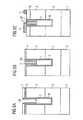
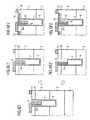
以下に、本発明を、実施例に基づいて図面を参照しながら詳述する。図1は、SNOR構造を示す概略的な等価回路図である。図2は、従来のビット線構造を有する図1にかかる配置を示す概略的な平面図である。図3は、本発明にかかるビット線構造を備えた半導体回路の配置を示す概略的な平面図である。図4は、第1実施例にかかるビット線構造を示すために図3に示した半導体回路構造の概略的な断面図を示す。図5A〜図5Iは、第1実施例にかかるビット線構造の製造方法に含まれる重要な工程を示す、概略的な断面図である。図6A〜図6F2は、第2または第3の実施形態にかかるビット線構造の製造方法に含まれる重要な工程を示す、概略的な断面図である。図7は、第4の実施形態にかかるビット線構造を示す概略断面図である。 Hereinafter, the present invention will be described in detail based on examples with reference to the drawings. FIG. 1 is a schematic equivalent circuit diagram showing the SNOR structure. FIG. 2 is a schematic plan view showing an arrangement according to FIG. 1 having a conventional bit line structure. FIG. 3 is a schematic plan view showing the arrangement of a semiconductor circuit having a bit line structure according to the present invention. FIG. 4 is a schematic cross-sectional view of the semiconductor circuit structure shown in FIG. 3 to show the bit line structure according to the first embodiment. 5A to 5I are schematic cross-sectional views showing important steps included in the method of manufacturing the bit line structure according to the first embodiment. 6A to 6F2 are schematic cross-sectional views showing important steps included in the method of manufacturing the bit line structure according to the second or third embodiment. FIG. 7 is a schematic sectional view showing the bit line structure according to the fourth embodiment.
図3に、例えばSNOR半導体メモリー回路に用いることができる、本発明にかかるビット線構造の概略的な平面図を示す。この図では、図1および図2に示した素子または層と同様のものには、同じ参照符号を付けている。 FIG. 3 shows a schematic plan view of a bit line structure according to the present invention that can be used in, for example, a SNOR semiconductor memory circuit. In this figure, elements similar to those shown in FIGS. 1 and 2 are given the same reference numerals.
図3によれば、帯状をなした複数のトレンチ分離STIによって、複数の能動領域AAが、帯状をなして、基板に縦列に形成されている。この基板は、例えば、半導体基板、好ましくはシリコンを含んでいる。また、ワード線積層WLx(x=1〜n)は、図2に示した従来技術と同様に、基板面において帯状をなして形成されている能動領域AAに対して、垂直方向に、横列に形成されている。これらのワード線積層は、例えば不揮発性メモリー素子を形成するために、ゲート酸化物層またはトンネル層といった第1絶縁層と、フローティングゲートといった電荷蓄積層と、中間誘電体のような第2絶縁層と、制御層とを、実駆動ワード線として備えている。絶縁のため、側壁絶縁層またはスペーサーSPは、ワード線積層WLxの側壁に形成されている。したがって、電界効果トランジスタ構造を実現するために第1・第2ドーピング領域としてのドレイン領域Dおよびソース領域Sをワード線積層の側面に有する、切替え素子または不揮発性メモリー素子SEが、能動領域AAとワード線積層WLxとの間の各交差点または重複点に形成される。 According to FIG. 3, a plurality of active regions AA are formed in tandem on the substrate in a strip shape by a plurality of trench isolation STIs in the strip shape. This substrate comprises, for example, a semiconductor substrate, preferably silicon. The word line stack WLx (x = 1 to n) is arranged in a row in the vertical direction with respect to the active area AA formed in a band shape on the substrate surface, as in the conventional technique shown in FIG. Is formed. These word line stacks include, for example, a first insulating layer such as a gate oxide layer or a tunnel layer, a charge storage layer such as a floating gate, and a second insulating layer such as an intermediate dielectric to form a nonvolatile memory element. And a control layer as actual drive word lines. For insulation, the sidewall insulating layer or spacer SP is formed on the sidewall of the word line stack WLx. Therefore, in order to realize the field effect transistor structure, the switching element or the non-volatile memory element SE having the drain region D and the source region S as the first and second doping regions on the side surface of the word line stack includes the active region AA. It is formed at each intersection or overlapping point with the word line stack WLx.
しかしながら、本発明にかかる領域最適化半導体回路を実現するためには、ソース線SLxとドレイン線DLx(x=1〜m)との対を備えたビット線構造が、基板面だけではなく、一方で基板内のトレンチ分離STI内に位置する埋め込みビット線SLxとして、かつ、他方で基板面または基板面上に位置する表面ビット線DLxとして形成される。すなわち、埋め込みビット線SLxを、トレンチ分離STIの下層に埋設し、局部的に形成された自動調心電極層13を介して、ソース領域Sに接続されている。一方、例えば第1金属被覆レベル内に形成されるような表面ビット線DLxは、接続部DCを介して、切替え素子SEのドレイン領域Dに接続される。これにより、所要面積に関して最適化でき、かつ、特に、間隔距離(構造の大きさ+構造の間隔)が十分に低減された、ビット線構造を提供することができる。 However, in order to realize the region-optimized semiconductor circuit according to the present invention, the bit line structure including the pair of the source line SLx and the drain line DLx (x = 1 to m) is not limited to the substrate surface. The buried bit line SLx located in the trench isolation STI in the substrate and the surface bit line DLx located on the substrate surface or the substrate surface on the other side. That is, the buried bit line SLx is buried in the lower layer of the trench isolation STI and is connected to the source region S through the self-aligning
図3では、表面ビット線DLxが、帯状をなして能動領域AAの上に形成されている。このような直線的な帯状の設計であるため、これらの能動領域は、比較的簡単な方法で、リソグラフィー的に(lithographically)規定することができる。このことは、後に重要とになる。しかしながら、表面ビット線は、同様に他の形状であってもよい。 In FIG. 3, the surface bit line DLx is formed on the active area AA in a band shape. Due to such a linear strip design, these active areas can be lithographically defined in a relatively simple manner. This will become important later. However, the surface bit lines may have other shapes as well.
図4は、図3で示した切断線A−Aに沿って切断した状態を概略的に示した断面図である。同じ素子または層には、同じ参照符号を付け、これらについての記載は省略する。 4 is a cross-sectional view schematically showing a state cut along the cutting line AA shown in FIG. The same reference numerals are given to the same elements or layers, and description thereof is omitted.
図4では、半導体基板は、多層構造または複数のウェル構造を備えている。この複数のウェル構造としては、第1のウェル構造として例えばp型ウェル3があり、第2のウェル構造として例えばn型ウェル2があり、これらが、実半導体基板(actual semiconductor substrate)1またはディープ(deep)p型ウェル1内に形成されている。このような複数のウェル構造は、特に、ウェル構造の遮蔽効果およびの絶縁特性に関し、利点を有するものである。なぜなら、例えば空間電荷領域(space charge regions)を用いることによって、基板の深度の深い領域であっても、絶縁層を十分に形成することができ、複雑な構造を実現することができるからである。 In FIG. 4, the semiconductor substrate has a multilayer structure or a plurality of well structures. As the plurality of well structures, there are, for example, a p-type well 3 as a first well structure, and, for example, an n-type well 2 as a second well structure. (Deep) It is formed in the p-type well 1. Such a plurality of well structures have advantages particularly with respect to the shielding effect and insulation characteristics of the well structures. This is because, for example, by using space charge regions, an insulating layer can be sufficiently formed even in a deep region of the substrate, and a complicated structure can be realized. .
また、トレンチの壁(トレンチ壁)としてトレンチ絶縁層6を備えたディープトレンチ(deep trenches)は、実半導体基板や、それに関連する層やウェル1、2、3中に形成される。実際の埋め込みビット線SLx(the actual buried bit line SLx)は、導電性充填層7を用いて、トレンチ絶縁層6を有するトレンチの下部に、形成されている。2分の1を被覆することが好ましい被覆部分層9を有する被覆絶縁層は、トレンチの上部における、一部分または片側にのみ形成される。この被覆絶縁層(被覆部分層9)は、STI(トレンチ分離)方法によって形成されることが好ましい。このようにして、図4では、特にトレンチの上部の左側において、優れた絶縁特性が形成されている。 Further, deep trenches having a
トレンチ上部の他の部分、または、トレンチの上部の右側には、第2ドーピング領域10またはソース領域Sに関連する絶縁層9およびトレンチ絶縁層6は、完全に除去され、その代わりに、複数の電極接続層12が形成されている。これらの層は、導電性であり、埋め込みビット線または導電性充填層7と接触している。第2ドーピング領域10は、絶縁トレンチ間の基板面に形成され、好ましくは、直接、絶縁トレンチに隣接して形成される。そして、これらの第2ドーピング領域10を、埋め込みビット線SLxに接続するために、自動調心電極層13が、基板面の領域に位置するマスク層11間に、また、図4に示したように基板面に直接、形成されている。これらの自動調心電極層13は、シリコン半導体材料である場合は、ケイ化物またはサリサイド(自己整合ケイ化物)から構成されている。 In the other part of the upper part of the trench, or on the right side of the upper part of the trench, the insulating
基板と、第2ドーピング領域10と、自動調心電極層13とを、これらの上に位置する層から絶縁するために、中間絶縁層14が形成されている。中間絶縁層14の表面には、最終的に、パターン化された(structured)表面ビット線DLxが、パターン化された導電層15として帯状に形成される。 An intermediate insulating
これにより、初めて、金属化レベルにおける間隔(構造寸法+構造幅)に関して要求性の低い、SNOR構造にも適した、領域が最適化されたビット線構造を得ることができる。 Thereby, for the first time, it is possible to obtain a bit line structure with an optimized region, which is also suitable for an SNOR structure, which is less required with respect to the interval (structure dimension + structure width) at the metallization level.
図4では、第2ドーピング領域10とは逆の伝導型p+の半導体材料(例えばSi)が、埋め込みビット線または導電性充填層7および被覆接続層12に使用される。具体的には、一例として、p+にドープされた半導体材料が導電性充填層7および被覆接続層12に使用され、一方で、ソース領域Sは、n+にドープされており、p型にドープされたウェル3に形成されている。トレンチの上部の一部分にトレンチ絶縁層6がないため、特に複数の被覆接続層12が、基板またはp型ウェル3に直接接続されているこのような構成では、被覆接続層12が、埋め込みビット線を用いてソース領域Sに接続できるだけでなく、p型ウェル3にも接続することができる。この結果、特に、例えばフラッシュEPROM素子のような不揮発性メモリー素子の場合、トンネル特性がより均質的になり、書き込み/消去サイクルの数(保持期間)を増やすことができる。さらに、結果として、寄生ダイオードまたは漏れ電流を著しく低減することができる。このように、基板または基板のウェル構造に、被覆接続層12を介した直接接続を形成する利点としては、このようなウェルの電位を均一にするために通常必要である表面接続を行う必要がないという点が挙げられる。したがって、このように、設計に関する強いられていた要求を著しく緩和することができる。In FIG. 4, a p+ semiconductor material (for example, Si) opposite to the
図5A〜図5Iに、図4に示したようなビット線構造の製造方法の中の重要な製造工程について、概略的な断面図を示して説明する。同じ参照符号が付されているものについては、上記と同様の素子または層を示しているため、以下では説明を省略する。 5A to 5I, an important manufacturing process in the manufacturing method of the bit line structure as shown in FIG. 4 will be described with reference to schematic cross-sectional views. Elements having the same reference numerals indicate elements or layers similar to those described above, and thus description thereof is omitted below.
すなわち、図5Aに示すように、複数のウェルを例えばイオン注入によって基板に形成する。これにより、例えば、ディープp型ウェル1、シャロー(shallow)第1ウェル3、および、第2n型ウェル2を形成する。言うまでもなく、ディープp型ウェル1は、それ自体が基板となっていてもよい。また、基板中に形成されるウェルの数を増やしてもよい。そして、半導体材料の表面に、第1補助絶縁層4を、例えば酸化物層を蒸着するか、または、成長させることによって形成する。その後、硬質マスク層5を形成・パターン化するとともに、第1補助絶縁層4の表面に窒化シリコンを形成する。硬質マスク層5を、従来のフォトリソグラフィー方法を用いてパターン化することで、後に形成されるトレンチがほぼ規定される。 That is, as shown in FIG. 5A, a plurality of wells are formed on the substrate by ion implantation, for example. Thereby, for example, a deep p-type well 1, a shallow
図5Bに示す断面図では、パターン化された硬質マスク5を用いて、ディープトレンチTを基板中に形成する。上記のした実施の形態では、このトレンチは、第2n型ウェル2まで延びている。この場合、例えば反応性イオンエッチング(RIE)のような異方性エッチング法を用いることが好ましい。このエッチング工程は、例えばポリマーまたはポリマーの残余物を除去する洗浄工程が行われることで終了する。 In the cross-sectional view shown in FIG. 5B, the deep trench T is formed in the substrate using the patterned
図5Cに示す断面図では、トレンチTの全トレンチ表面に、トレンチ絶縁層6を形成する。この際、いわゆる線酸化物(liner oxide)を形成するために、熱酸化が行われることが好ましい。しかしながら、原理的には、トレンチ絶縁層6に、二酸化シリコン以外の他の絶縁層を用いることもでき、特に、多層の絶縁層を実現することもできる。 In the cross-sectional view shown in FIG. 5C, the
次に、導電性充填層7を、トレンチTの中またはトレンチ絶縁層6の表面に沿って形成することにより、埋め込みビット線を形成する。このような場合、トレンチとして、高ドープされたポリシリコンを蒸着することが好ましく、ドーピングは、用いられるシャロー第1ウェル3および、形成される意図的な接続として選択される。しかしながら、原理的には、例えば金属のような他の導電層を、埋め込みビット線SLxとしてトレンチの中に形成してもよい。 Next, by forming the
図5Dに示す断面図では、次の工程において、まず、導電性充填層7を窪みに配置する。この際、シャロートレンチ分離を実現するため、およびシャロートレンチSTを形成するために、例えば、STI処理を用いることができる。なお、このような従来のSTI処理に含まれる各工程については、通常、当業者にとって周知であるため、これ以上詳述しない。 In the cross-sectional view shown in FIG. At this time, for example, STI processing can be used to realize shallow trench isolation and to form the shallow trench ST. Note that each step included in such a conventional STI process is generally well known to those skilled in the art and will not be described in further detail.
図5Eに示す断面図では、この場合は、好ましい異方性エッチング工程の後に、硬質マスク層5のトレンチエッジ部分に対してエッチバックを施すことも可能であり、これはいわゆる「窒化物引戻し(nitride pullback)」と呼ばれるものである。これにより、続く処理工程に対して、トレンチエッジ部分における応力(負荷)をある程度低減でき、さらに、半導体回路に同様に存在している例えばCMOSトランジスタの電気特性を、改善することにもなる。 In the cross-sectional view shown in FIG. 5E, in this case, it is possible to etch back the trench edge portion of the
またその後、絶縁層である第1被覆部分層8を、エッチバックされた導電性充填層7の表面に形成することもできる。この場合、再度、熱酸化を行い、別の線酸化物を形成することが好ましい。最後に、他の絶縁層である第2被覆部分層9を形成する。このとき、トレンチの上部に、TEOS蒸着処理によって二酸化シリコンを完全に充填することが好ましい。そして、硬質マスク層5を阻止層として使用する例えばCMP(化学的機械研磨)処理のような平坦化処理によって、図5Eの断面図に示した構造となる。 Thereafter, the first covering partial layer 8 that is an insulating layer can also be formed on the surface of the
図5Fに示す断面図では、硬質マスク層5または窒化シリコンは完全に除去される。同様に、第1補助絶縁層4を除去してもよい。この時点で例えば、第1絶縁層(図示せず)またはゲート酸化物層またはトンネル酸化物層が、半導体基板の能動領域AAの各領域に形成される。しかしながら、このような第1絶縁層は、断面図では必要ではない。結果として、第1絶縁層を除去し、図示した第2ドーピング領域10を、ソースおよびドレイン領域として、半導体基板の表面に形成する。これらのドーピング領域10は、例えば、従来の注入方法によって形成される。各スペーサーを用いてLDD注入または接続注入を行ってもよい。 In the cross-sectional view shown in FIG. 5F, the
また、図5Gに示す断面図では、マスク層11またはキャップ層11が、トレンチの一部分のみ、例えば片側のみを覆うように、パターン化されて形成されている。このマスク層11を形成するために、例えば二酸化シリコンまたは窒化シリコンが蒸着・パターン化される。また、例えば新しいタイプの金属酸化物(ZrO2、Al2O3、…)のような他の材料を用いてもよい。In the cross-sectional view shown in FIG. 5G, the
図5Hに示す断面図では、トレンチ絶縁層6と、第1被覆部分層8と、第2被覆部分層9とを備えた被覆絶縁層の、マスク層11によって被覆されていない部分を、導電性充填層7が露出するまで、例えば強い選択的異方性酸化物エッチング処理を行うことにより、完全に除去する。これを、オーバーエッチング(図示せず)またはトレンチ絶縁層6のさらなる除去(図4参照)によって行ってもよい。 In the cross-sectional view shown in FIG. 5H, the portion of the covering insulating layer including the
また、図5Iに示す断面図では、被覆接続層12が、または、トレンチ全体を上から見た場合では多数の被覆接続層が、トレンチのエッチバック部分領域内の対応する箇所に形成される。このとき、蒸着時にドープされる(in situ-doped)ポリシリコンを蒸着することが好ましい。 Further, in the cross-sectional view shown in FIG. 5I, the
導電性充填層7に被覆接続層12を導電的に接続した後、基板中の第1および第2ドーピング領域10はさらにエッチバックされる。これにより、被覆接続層12が残存することが原因で隣り合うソース領域間に寄生漏電が生じるようなことを確実になくすことができる。そして、多数の自動調心電極層13を、被覆接続層12と第1および第2ドーピング領域10との表面に形成し、結果として、第1および第2ドーピング領域10と、被覆絶縁層12または埋め込みビット線との間で導電的接続が生じることになる。このような導電性の高い接続領域13を形成するために、例えば、まず基板全面に、ケイ素化合物になりうる(silicidable)材料、または、例えばコバルト、ニッケル、または、プラチナのような、ケイ素化合物になりうる金属層を蒸着させる。次に、導電性の高い接続領域13を形成するために、半導体材料の表面層と、被覆接続層12と、ドーピング領域10とを、ケイ素化合物になりうる材料を用いて転換する。このとき、半導体材料(シリコン)に接続していない表面、つまりマスク層11には、ケイ素化合物を形成しないが、これらの表面には、蒸着された材料(金属)が残っている。したがって、蒸着された(しかしケイ素化合物化されていない)金属層を、好ましくはウェット化学エッチング処理によって再び選択的にエッチバックできる。このように、被覆接続層12および自動調心電極層13の両方の自動調心構成を、1つのマスクまたはマスク11を用いて行うことができる。さらに、適切なドーピング材料を選択したならば、第1ウェル3を有した直接接続を形成することができる。 After conductively connecting the
図示はしないが、続く工程では、表面ビット線DLxを実現するために、例えば、再びマスク層11を再び除去したり、図4に示した中間絶縁層14、および金属被膜層15を形成・パターン化することができる。最後に、表面ビット線(DLx)を第1ドーピング領域(B)に導電的に接続するための複数の接触部(DC)を形成する。 Although not shown, in the subsequent process, in order to realize the surface bit line DLx, for example, the
また、図6A〜図6F2は、第2または第3の実施形態におけるビット線構造の製造方法に含まれる重要な製造工程を示す概略的な簡単な断面図である。図1〜図5に示した層と同様の層については同じ参照符号を付し、以下では説明を省略する。 FIGS. 6A to 6F2 are schematic cross-sectional views showing important manufacturing steps included in the method of manufacturing the bit line structure in the second or third embodiment. The same layers as those shown in FIGS. 1 to 5 are denoted by the same reference numerals, and description thereof will be omitted below.
まずは、再度、図5A〜図5Dに沿って、トレンチTと、トレンチ絶縁層6と、エッチバック充填層7とを形成する前工程を行う。ここから、この工程について、具体的に説明する。 First, a pre-process for forming the trench T, the
図6Aでは、例えば図5Dに示したような工程の後、トレンチの上部は、第1被覆部分層8および第2被覆部分層9によって完全に充填されない。しかしながら、初めに、例えばスペーサー方法によって、トレンチの上部におけるトレンチ絶縁層6の表面に、被覆犠牲層8Aを形成する。この被覆犠牲層8Aは、ここでは、トレンチ絶縁層6および次に形成される絶縁充填層9とは異なるエッチング選択性を有している。このようなスペーサー方法(絶縁(conformal)層の形成および、異方性エッチバック)については、通常、当業者にとって周知であるので、以下では記載しない。 In FIG. 6A, after the step as shown in FIG. 5D, for example, the upper part of the trench is not completely filled with the first covering portion layer 8 and the second
図6Bでは、図5Eに示した方法ステップと同様に、トレンチを完全に充填するための第2充填部分層9を、例えばTEOS蒸着処理によって形成する。そして、平坦化処理(CMP)を行って、硬質マスク層5を除去する。 In FIG. 6B, similar to the method step shown in FIG. 5E, the second filling
次に、図6Cでは、マスク層11を基板面に形成・パターン化する。このパターン化は、少なくともトレンチの一部分をマスク層11によって覆うように行われる。このとき、マスク層11が、トレンチの半分、または、トレンチの上部に位置するトレンチ絶縁体の半分を覆うことが好ましい。 Next, in FIG. 6C, the
次に、図6Dでは、第2の実施形態によれば、選択性の高い等方性エッチング工程を行うことにより、被覆犠牲層8Aを除去することができる。この場合、例えば、窒化シリコン層を被覆犠牲層8Aとして使用し、リン酸をエッチング液として用いることができる。しかしながら、このような場合の不都合な点としては、例えば、シリコン層をマスク層11に用いることができない点にある。しかしながら、その代わりに、例えばAl2O3、ZrO2、HfO2などのような絶縁層がマスク層11に適している。Next, in FIG. 6D, according to the second embodiment, the covering
これにより、基板または第1ウェル3に対して、トレンチ絶縁層6によって完全に絶縁された、導電性充填層7となるコンタクトホールが生じる。その結果、特定の用途に対して、絶縁特性が改善され、かつ、個々の表面領域が低減される。なぜなら、この場合、自動調心であるため、ずれに対応する通常の写真技術調整(photographic technolog reserve)を取り入れる必要がないからである。 As a result, a contact hole serving as the
したがって、図6E1に示した第2の実施形態では、上部の被覆されていない、または、マスクされていない領域にも、トレンチ絶縁層6を形成しておく。この結果、さらに、その後行われるドーピング領域10の薄層化またはこの領域への凹部の形成中のオーバーエッチングによる危険性が、低減される。 Therefore, in the second embodiment shown in FIG. 6E1, the
また、図6F1では、被覆接続層12が、図5Iに示したように再び形成され、ドーピング領域10は(任意で)凹状にされ、導電性の高い接続層13は自動調心的に(in a self-aligning fashion)形成される。この結果、埋め込みビット線構造が生じる。この埋め込みビット線構造は、埋め込みビット線が基板または第1ウェル3に接続しておらず、接続電位に対する自由度が高い。 Also, in FIG. 6F1, the
一方、図6E2に示す第3の実施形態では、今度は、好ましくはマスク層11を用いたさらなるウェット化学エッチング処理によって、トレンチ絶縁層6をトレンチの露出した上部から完全に除去することができる。これにより、今度は、使用された半導体材料の適切なドーピングにより、基板または第1ウェル3への直接接続が生じる。 On the other hand, in the third embodiment shown in FIG. 6E2, the
図6F2に、被覆接続層12および導電性の高い電極層13を形成するための最終工程を示す。(この工程については、図5Iに関する記載を参照)
図7に、第4の実施形態にかかるビット線構造の概略的な断面図を示す。特に図4に示した層と同様の層には同じ参照符号を付し、説明は省略する。FIG. 6F2 shows a final process for forming the
FIG. 7 is a schematic cross-sectional view of the bit line structure according to the fourth embodiment. In particular, the same layers as those shown in FIG.
図7に示した構造は、導電性充填層7および被覆接続層12を形成するために、ドーピング領域10と同じ伝導型を有する半導体材料を使用する点以外は、図4に示した構造とほぼ同じ構造ある。具体的には、n+にドープされたソース領域Sとの導電的接続をすでに形成した蒸着時にドープされるn+ポリシリコンを、例えば導電性充填層7および被覆接続層12として使用する。しかしながら、被覆接続層12と、基板または第1ウェル3とが、逆の伝導型のドーピングを有しているので、いわゆる空乏領域または空間電荷領域(図6F1に示した第2の実施形態におけるトレンチ絶縁層6と同様の絶縁効果が生じる)が、被覆接続層12と基板または第1ウェル3との間の接続面に形成される。このようにして、埋め込みビット線と基板または対応するウェルとの間のウェル絶縁を、図5に示した方法および図6に示したの第2の実施形態を用いた場合でも、実行できる。The structure shown in FIG. 7 is almost the same as the structure shown in FIG. 4 except that a semiconductor material having the same conductivity type as that of the
さらに、本発明では、導電性の高い電極層13を、基板内に形成する必要はなく、すなわち、導電性の高い電極層13をドーピング領域10に埋め込む必要はなく、同様の方法によって、導電性の高い電極層13が、部分的または全体的に基板面に形成されるようにすることも可能である。 Furthermore, in the present invention, it is not necessary to form the
本発明は、不揮発性SNOR半導体メモリー回路に基づいて説明した。しかしながら、本発明はこの用途に限定するものではなく、むしろ、本発明は、対応するビット線構造を備えた他の半導体メモリー回路にも同様に適用することができる。さらに、本発明は、上述したようなシリコン半導体基板および材料に限定するものではなく、ドーピングまたは絶縁構造を有する他の半導体材料も、同様に適用できるものである。 The present invention has been described based on a nonvolatile SNOR semiconductor memory circuit. However, the present invention is not limited to this application, but rather, the present invention can be applied to other semiconductor memory circuits having a corresponding bit line structure as well. Further, the present invention is not limited to the silicon semiconductor substrate and materials as described above, and other semiconductor materials having a doping or insulating structure can be similarly applied.
1、2、3 基板またはそのウェル
4 第1補助絶縁層
5 硬質マスク層
6 トレンチ絶縁層
7 充填層
8 第1被覆部分層
9 第2被覆部分層
8A 被覆犠牲層
10 ドーピング領域
11 マスク層
12 被覆接続層
13 電極層
14 中間絶縁層
15 金属被覆層
T トレンチ
SLX 埋め込みビット線
DLx 表面ビット線
BLx 対のビット線
WLx ワード線
SE 切替え素子
K、DC 接続部
STI トレンチ分離
AA 能動領域
S ソース領域
D ドレイン領域1, 2 or 3 substrate or its well 4 first auxiliary insulating
Claims (21)
Translated fromJapanese複数の第2ドーピング領域(S;10)を接続するための、基板(1,2,3)の内部に形成された埋め込みビット線(SLx)とを備えたビット線構造であって、
上記基板(1,2,3)内に設けられたトレンチ(T)と、
上記トレンチ(T)のトレンチ表面に設けられたトレンチ絶縁層(6)と、
上記トレンチ絶縁層(6)に沿ってトレンチ(T)の下部に設けられた埋め込みビット線(SLx、7)と、
トレンチ(T)の第1上部領域内における上記埋め込みビット線(SLx)の上に設けられた被覆絶縁層(8,8A,9)と、
トレンチ(T)の第2上部領域内における上記埋め込みビット線(SLx)の上に設けられた複数の被覆接続層(12)と、
上記基板面に設けられた複数の自動調心電極層(13)とが、形成されており、
上記複数の被覆接続層(12)は、自動調心電極層(13)を介して、上記複数の第2ドーピング領域(S、10)に導電的に接続されていることを特徴とするビット線構造。A surface bit line (DLx) formed on the substrate surface for connecting the plurality of first doping regions (D);
A bit line structure including a buried bit line (SLx) formed in a substrate (1, 2, 3) for connecting a plurality of second doping regions (S; 10),
A trench (T) provided in the substrate (1, 2, 3);
A trench insulating layer (6) provided on the trench surface of the trench (T);
Embedded bit lines (SLx, 7) provided under the trench (T) along the trench insulating layer (6);
A covering insulating layer (8, 8A, 9) provided on the buried bit line (SLx) in the first upper region of the trench (T);
A plurality of covering connection layers (12) provided on the buried bit line (SLx) in the second upper region of the trench (T);
A plurality of self-aligning electrode layers (13) provided on the substrate surface are formed,
The bit line, wherein the plurality of covering connection layers (12) are electrically connected to the plurality of second doping regions (S, 10) via self-aligning electrode layers (13). Construction.
工程a) 基板(1,2,3)にトレンチ(T)を形成し、
工程b) 上記トレンチ(T)のトレンチ表面にトレンチ絶縁層(6)を形成し、
工程c) 埋め込みビット線(SLx)を実現するために、上記トレンチ(T)のトレンチ絶縁層(6)に沿って導電性充填層(7)を形成し、
工程d) 上記トレンチ(T)の上部領域に、被覆絶縁層(8,9,8A)を形成し、
工程e) 上記基板(3)の表面に、第1および第2ドーピング領域(10)を形成し、
工程f) 被覆絶縁層(8,9,8A)の部分領域における上記導電性充填層(7)上に、複数の被覆接続層(12)を形成し、
工程g) 上記複数の被覆接続層(12)を第2ドーピング領域(10、S)に導電的に接続するための、複数の自動調心電極層(13)を形成し、
工程h) 上記基板面に中間絶縁層(14)を形成し、
工程i) 表面ビット線(DLx)として導電層(15)を形成し、
工程j) 上記表面ビット線(DLx)を第1ドーピング領域(D)に導電的に接続するための、複数の接続部(DC)を形成する、工程a)〜j)を含むことを特徴とするビット線構造の製造方法。A method of manufacturing a bit line structure,
Step a) A trench (T) is formed in the substrate (1, 2, 3),
Step b) forming a trench insulating layer (6) on the trench surface of the trench (T),
Step c) In order to realize the buried bit line (SLx), a conductive filling layer (7) is formed along the trench insulating layer (6) of the trench (T),
Step d) Forming a covering insulating layer (8, 9, 8A) on the upper region of the trench (T),
Step e) forming first and second doping regions (10) on the surface of the substrate (3);
Step f) On the conductive filling layer (7) in the partial region of the covering insulating layer (8, 9, 8A), a plurality of covering connection layers (12) are formed,
Step g) forming a plurality of self-aligning electrode layers (13) for electrically connecting the plurality of coated connection layers (12) to the second doping region (10, S);
Step h) forming an intermediate insulating layer (14) on the substrate surface;
Step i) forming a conductive layer (15) as a surface bit line (DLx);
Step j) includes steps a) to j) for forming a plurality of connecting portions (DC) for electrically connecting the surface bit line (DLx) to the first doping region (D). A method of manufacturing a bit line structure.
Applications Claiming Priority (2)
| Application Number | Priority Date | Filing Date | Title |
|---|---|---|---|
| DE10240436ADE10240436C1 (en) | 2002-09-02 | 2002-09-02 | Bit line structure comprises a surface bit line, a trenched bit line, a trench isolation layer, a covering isolation layer, covering connecting layers, and self-adjusting connecting layers |
| PCT/DE2003/002676WO2004023553A2 (en) | 2002-09-02 | 2003-08-08 | Bitline structure and method for production thereof |
Publications (2)
| Publication Number | Publication Date |
|---|---|
| JP2006502565Atrue JP2006502565A (en) | 2006-01-19 |
| JP4080485B2 JP4080485B2 (en) | 2008-04-23 |
Family
ID=29557885
Family Applications (1)
| Application Number | Title | Priority Date | Filing Date |
|---|---|---|---|
| JP2004533202AExpired - Fee RelatedJP4080485B2 (en) | 2002-09-02 | 2003-08-08 | Bit line structure and manufacturing method thereof |
Country Status (7)
| Country | Link |
|---|---|
| US (3) | US20060043420A1 (en) |
| EP (1) | EP1472738B1 (en) |
| JP (1) | JP4080485B2 (en) |
| CN (1) | CN100350616C (en) |
| DE (2) | DE10240436C1 (en) |
| TW (1) | TWI251323B (en) |
| WO (1) | WO2004023553A2 (en) |
Cited By (1)
| Publication number | Priority date | Publication date | Assignee | Title |
|---|---|---|---|---|
| JP2009094214A (en)* | 2007-10-05 | 2009-04-30 | Toshiba Corp | Nonvolatile semiconductor memory device and manufacturing method thereof |
Families Citing this family (14)
| Publication number | Priority date | Publication date | Assignee | Title |
|---|---|---|---|---|
| DE10321739A1 (en)* | 2003-05-14 | 2004-12-09 | Infineon Technologies Ag | Bit line structure and method for its production |
| US7679130B2 (en) | 2005-05-10 | 2010-03-16 | Infineon Technologies Ag | Deep trench isolation structures and methods of formation thereof |
| JP2006324584A (en)* | 2005-05-20 | 2006-11-30 | Sharp Corp | Semiconductor device and manufacturing method thereof |
| US7888196B2 (en)* | 2008-12-29 | 2011-02-15 | Texas Instruments Incorporated | Trench isolation comprising process having multiple gate dielectric thicknesses and integrated circuits therefrom |
| US8138541B2 (en) | 2009-07-02 | 2012-03-20 | Micron Technology, Inc. | Memory cells |
| US20110042722A1 (en)* | 2009-08-21 | 2011-02-24 | Nanya Technology Corp. | Integrated circuit structure and memory array |
| TWI425521B (en)* | 2009-12-31 | 2014-02-01 | Taiwan Memory Corp | Method of forming bit line |
| KR101867998B1 (en)* | 2011-06-14 | 2018-06-15 | 삼성전자주식회사 | Method of forming a pattern |
| US10586765B2 (en)* | 2017-06-22 | 2020-03-10 | Tokyo Electron Limited | Buried power rails |
| CN110010605B (en)* | 2018-01-04 | 2021-04-02 | 中芯国际集成电路制造(上海)有限公司 | Memory and working method and forming method thereof |
| JP2020119929A (en)* | 2019-01-21 | 2020-08-06 | キオクシア株式会社 | Semiconductor device |
| CN114373753B (en)* | 2020-10-15 | 2024-10-25 | 长鑫存储技术有限公司 | Buried bit line and method for forming the same |
| US11877440B2 (en) | 2020-10-15 | 2024-01-16 | Changxin Memory Technologies, Inc. | Bit line structure including ohmic contact and forming method thereof |
| CN114373718B (en) | 2020-10-15 | 2024-10-29 | 长鑫存储技术有限公司 | Semiconductor device and method for manufacturing the same |
Family Cites Families (10)
| Publication number | Priority date | Publication date | Assignee | Title |
|---|---|---|---|---|
| US5430673A (en)* | 1993-07-14 | 1995-07-04 | United Microelectronics Corp. | Buried bit line ROM with low bit line resistance |
| JP2935346B2 (en)* | 1996-07-30 | 1999-08-16 | 日本電気株式会社 | Semiconductor device and manufacturing method thereof |
| TW379417B (en)* | 1998-06-04 | 2000-01-11 | United Semiconductor Corp | Buried bitline structure and the manufacture method |
| TW408450B (en)* | 1999-03-29 | 2000-10-11 | United Microelectronics Corp | Manufacture of the flash memory |
| WO2001047019A1 (en)* | 1999-12-20 | 2001-06-28 | Infineon Technologies Ag | Non-volatile nor semiconductor memory device and method for the programming thereof |
| US6348374B1 (en)* | 2000-06-19 | 2002-02-19 | International Business Machines | Process for 4F2 STC cell having vertical MOSFET and buried-bitline conductor structure |
| US6911687B1 (en)* | 2000-06-21 | 2005-06-28 | Infineon Technologies Ag | Buried bit line-field isolation defined active semiconductor areas |
| DE10062245A1 (en)* | 2000-12-14 | 2002-07-04 | Infineon Technologies Ag | Non-volatile semiconductor memory cell and associated semiconductor circuit arrangement and method for the production thereof |
| US6777725B2 (en)* | 2002-06-14 | 2004-08-17 | Ingentix Gmbh & Co. Kg | NROM memory circuit with recessed bitline |
| US6734482B1 (en)* | 2002-11-15 | 2004-05-11 | Micron Technology, Inc. | Trench buried bit line memory devices |
- 2002
- 2002-09-02DEDE10240436Apatent/DE10240436C1/ennot_activeExpired - Fee Related
- 2003
- 2003-07-24TWTW092120295Apatent/TWI251323B/ennot_activeIP Right Cessation
- 2003-08-08CNCNB038076187Apatent/CN100350616C/ennot_activeExpired - Fee Related
- 2003-08-08EPEP03793593Apatent/EP1472738B1/ennot_activeExpired - Lifetime
- 2003-08-08JPJP2004533202Apatent/JP4080485B2/ennot_activeExpired - Fee Related
- 2003-08-08DEDE50312828Tpatent/DE50312828D1/ennot_activeExpired - Lifetime
- 2003-08-08WOPCT/DE2003/002676patent/WO2004023553A2/enactiveApplication Filing
- 2004
- 2004-03-18USUS10/513,163patent/US20060043420A1/enactiveGranted
- 2004-03-18USUS10/513,163patent/US7176088B2/ennot_activeExpired - Fee Related
- 2006
- 2006-11-02USUS11/592,844patent/US7291881B2/ennot_activeExpired - Fee Related
Cited By (1)
| Publication number | Priority date | Publication date | Assignee | Title |
|---|---|---|---|---|
| JP2009094214A (en)* | 2007-10-05 | 2009-04-30 | Toshiba Corp | Nonvolatile semiconductor memory device and manufacturing method thereof |
Also Published As
| Publication number | Publication date |
|---|---|
| CN1647280A (en) | 2005-07-27 |
| US20060043420A1 (en) | 2006-03-02 |
| US7176088B2 (en) | 2007-02-13 |
| US7291881B2 (en) | 2007-11-06 |
| US20070049050A1 (en) | 2007-03-01 |
| DE50312828D1 (en) | 2010-08-05 |
| EP1472738B1 (en) | 2010-06-23 |
| WO2004023553A2 (en) | 2004-03-18 |
| EP1472738A2 (en) | 2004-11-03 |
| TWI251323B (en) | 2006-03-11 |
| TW200406904A (en) | 2004-05-01 |
| JP4080485B2 (en) | 2008-04-23 |
| DE10240436C1 (en) | 2003-12-18 |
| WO2004023553A3 (en) | 2004-06-03 |
| CN100350616C (en) | 2007-11-21 |
Similar Documents
| Publication | Publication Date | Title |
|---|---|---|
| US7291881B2 (en) | Bit line structure and method of fabrication | |
| KR100391985B1 (en) | Method of making a scalable two transistor memory device | |
| JP4276510B2 (en) | Semiconductor memory device and manufacturing method thereof | |
| US6064105A (en) | Data retention of EEPROM cell with shallow trench isolation using thicker liner oxide | |
| US6570215B2 (en) | Nonvolatile memories with floating gate spacers, and methods of fabrication | |
| US7211858B2 (en) | Split gate storage device including a horizontal first gate and a vertical second gate in a trench | |
| US6784039B2 (en) | Method to form self-aligned split gate flash with L-shaped wordline spacers | |
| TWI784724B (en) | Split-gate, 2-bit non-volatile memory cell with erase gate disposed over word line gate, and method of making same | |
| US7186607B2 (en) | Charge-trapping memory device and method for production | |
| JP2008098519A (en) | Nonvolatile semiconductor memory | |
| US20050196913A1 (en) | Floating gate memory structures and fabrication methods | |
| JP4053232B2 (en) | Semiconductor integrated circuit device and manufacturing method thereof | |
| CN111146203A (en) | Manufacturing method of 3D NOR flash memory and memory cell structure thereof | |
| US7129540B2 (en) | Semiconductor circuit arrangement with trench isolation and fabrication method | |
| JP2007005380A (en) | Semiconductor device | |
| US6916701B2 (en) | Method for fabricating a silicide layer of flat cell memory | |
| CN113053905B (en) | Memory element and method for manufacturing the same | |
| US9882033B2 (en) | Method of manufacturing a non-volatile memory cell and array having a trapping charge layer in a trench | |
| US20070138538A1 (en) | Method of forming self-aligned floating gate array and flash memory device including self-aligned floating gate array | |
| US7358559B2 (en) | Bi-directional read/program non-volatile floating gate memory array, and method of formation | |
| US20050156225A1 (en) | Methods of fabricating semiconductor devices with scalable two transistor memory cells | |
| JP2010186817A (en) | Semiconductor device and method of manufacturing the same | |
| KR20060062791A (en) | Nonvolatile Memory Device and Manufacturing Method Thereof | |
| JP2011035319A (en) | Semiconductor device and method of manufacturing the same |
Legal Events
| Date | Code | Title | Description |
|---|---|---|---|
| A977 | Report on retrieval | Free format text:JAPANESE INTERMEDIATE CODE: A971007 Effective date:20061130 | |
| A131 | Notification of reasons for refusal | Free format text:JAPANESE INTERMEDIATE CODE: A131 Effective date:20071016 | |
| A521 | Request for written amendment filed | Free format text:JAPANESE INTERMEDIATE CODE: A523 Effective date:20071207 | |
| RD02 | Notification of acceptance of power of attorney | Free format text:JAPANESE INTERMEDIATE CODE: A7422 Effective date:20071207 | |
| TRDD | Decision of grant or rejection written | ||
| A01 | Written decision to grant a patent or to grant a registration (utility model) | Free format text:JAPANESE INTERMEDIATE CODE: A01 Effective date:20080108 | |
| A61 | First payment of annual fees (during grant procedure) | Free format text:JAPANESE INTERMEDIATE CODE: A61 Effective date:20080206 | |
| FPAY | Renewal fee payment (event date is renewal date of database) | Free format text:PAYMENT UNTIL: 20110215 Year of fee payment:3 | |
| R150 | Certificate of patent or registration of utility model | Free format text:JAPANESE INTERMEDIATE CODE: R150 | |
| FPAY | Renewal fee payment (event date is renewal date of database) | Free format text:PAYMENT UNTIL: 20120215 Year of fee payment:4 | |
| FPAY | Renewal fee payment (event date is renewal date of database) | Free format text:PAYMENT UNTIL: 20130215 Year of fee payment:5 | |
| FPAY | Renewal fee payment (event date is renewal date of database) | Free format text:PAYMENT UNTIL: 20140215 Year of fee payment:6 | |
| R250 | Receipt of annual fees | Free format text:JAPANESE INTERMEDIATE CODE: R250 | |
| R250 | Receipt of annual fees | Free format text:JAPANESE INTERMEDIATE CODE: R250 | |
| R250 | Receipt of annual fees | Free format text:JAPANESE INTERMEDIATE CODE: R250 | |
| R250 | Receipt of annual fees | Free format text:JAPANESE INTERMEDIATE CODE: R250 | |
| LAPS | Cancellation because of no payment of annual fees |