JP2006501699A - Broadband flat inverted F antenna - Google Patents
Broadband flat inverted F antennaDownload PDFInfo
- Publication number
- JP2006501699A JP2006501699AJP2003575451AJP2003575451AJP2006501699AJP 2006501699 AJP2006501699 AJP 2006501699AJP 2003575451 AJP2003575451 AJP 2003575451AJP 2003575451 AJP2003575451 AJP 2003575451AJP 2006501699 AJP2006501699 AJP 2006501699A
- Authority
- JP
- Japan
- Prior art keywords
- radiating element
- plane
- antenna
- edge
- ground plane
- Prior art date
- Legal status (The legal status is an assumption and is not a legal conclusion. Google has not performed a legal analysis and makes no representation as to the accuracy of the status listed.)
- Pending
Links
- 230000008878couplingEffects0.000claimsabstractdescription10
- 238000010168coupling processMethods0.000claimsabstractdescription10
- 238000005859coupling reactionMethods0.000claimsabstractdescription10
- 239000000758substrateSubstances0.000claimsdescription31
- RYGMFSIKBFXOCR-UHFFFAOYSA-NCopperChemical compound[Cu]RYGMFSIKBFXOCR-UHFFFAOYSA-N0.000claimsdescription18
- 229910052802copperInorganic materials0.000claimsdescription12
- 239000010949copperSubstances0.000claimsdescription12
- 239000004020conductorSubstances0.000claimsdescription10
- 229910000906BronzeInorganic materials0.000claimsdescription9
- BQCADISMDOOEFD-UHFFFAOYSA-NSilverChemical compound[Ag]BQCADISMDOOEFD-UHFFFAOYSA-N0.000claimsdescription9
- 238000004519manufacturing processMethods0.000claimsdescription9
- 230000002093peripheral effectEffects0.000claimsdescription9
- OKTJSMMVPCPJKN-UHFFFAOYSA-NCarbonChemical compound[C]OKTJSMMVPCPJKN-UHFFFAOYSA-N0.000claimsdescription8
- 229910052782aluminiumInorganic materials0.000claimsdescription8
- XAGFODPZIPBFFR-UHFFFAOYSA-NaluminiumChemical compound[Al]XAGFODPZIPBFFR-UHFFFAOYSA-N0.000claimsdescription8
- 229910002804graphiteInorganic materials0.000claimsdescription8
- 239000010439graphiteSubstances0.000claimsdescription8
- 239000010974bronzeSubstances0.000claimsdescription6
- 239000011889copper foilSubstances0.000claimsdescription6
- KUNSUQLRTQLHQQ-UHFFFAOYSA-Ncopper tinChemical compound[Cu].[Sn]KUNSUQLRTQLHQQ-UHFFFAOYSA-N0.000claimsdescription6
- 229910052709silverInorganic materials0.000claimsdescription6
- 239000004332silverSubstances0.000claimsdescription6
- 239000004744fabricSubstances0.000claimsdescription5
- 238000000034methodMethods0.000claimsdescription5
- 239000011888foilSubstances0.000claimsdescription3
- PCHJSUWPFVWCPO-UHFFFAOYSA-NgoldChemical compound[Au]PCHJSUWPFVWCPO-UHFFFAOYSA-N0.000claimsdescription3
- 239000010935stainless steelSubstances0.000claimsdescription3
- 229910001220stainless steelInorganic materials0.000claimsdescription3
- PEZNEXFPRSOYPL-UHFFFAOYSA-N(bis(trifluoroacetoxy)iodo)benzeneChemical compoundFC(F)(F)C(=O)OI(OC(=O)C(F)(F)F)C1=CC=CC=C1PEZNEXFPRSOYPL-UHFFFAOYSA-N0.000claims1
- 238000010586diagramMethods0.000description12
- 230000008901benefitEffects0.000description6
- 230000006872improvementEffects0.000description5
- 229910052751metalInorganic materials0.000description3
- 239000002184metalSubstances0.000description3
- ORQBXQOJMQIAOY-UHFFFAOYSA-NnobeliumChemical compound[No]ORQBXQOJMQIAOY-UHFFFAOYSA-N0.000description3
- 239000011248coating agentSubstances0.000description2
- 238000000576coating methodMethods0.000description2
- 238000004891communicationMethods0.000description2
- 230000001419dependent effectEffects0.000description2
- ATJFFYVFTNAWJD-UHFFFAOYSA-NTinChemical compound[Sn]ATJFFYVFTNAWJD-UHFFFAOYSA-N0.000description1
- 238000010521absorption reactionMethods0.000description1
- 230000005540biological transmissionEffects0.000description1
- 230000001413cellular effectEffects0.000description1
- 230000007423decreaseEffects0.000description1
- 230000005611electricityEffects0.000description1
- 229910001092metal group alloyInorganic materials0.000description1
- 238000012986modificationMethods0.000description1
- 230000004048modificationEffects0.000description1
- 238000007747platingMethods0.000description1
- 230000009467reductionEffects0.000description1
- 125000006850spacer groupChemical group0.000description1
Images


Classifications
- H—ELECTRICITY
- H01—ELECTRIC ELEMENTS
- H01Q—ANTENNAS, i.e. RADIO AERIALS
- H01Q1/00—Details of, or arrangements associated with, antennas
- H01Q1/36—Structural form of radiating elements, e.g. cone, spiral, umbrella; Particular materials used therewith
- H01Q1/38—Structural form of radiating elements, e.g. cone, spiral, umbrella; Particular materials used therewith formed by a conductive layer on an insulating support
- H—ELECTRICITY
- H01—ELECTRIC ELEMENTS
- H01Q—ANTENNAS, i.e. RADIO AERIALS
- H01Q1/00—Details of, or arrangements associated with, antennas
- H01Q1/12—Supports; Mounting means
- H01Q1/22—Supports; Mounting means by structural association with other equipment or articles
- H01Q1/24—Supports; Mounting means by structural association with other equipment or articles with receiving set
- H01Q1/241—Supports; Mounting means by structural association with other equipment or articles with receiving set used in mobile communications, e.g. GSM
- H01Q1/242—Supports; Mounting means by structural association with other equipment or articles with receiving set used in mobile communications, e.g. GSM specially adapted for hand-held use
- H01Q1/243—Supports; Mounting means by structural association with other equipment or articles with receiving set used in mobile communications, e.g. GSM specially adapted for hand-held use with built-in antennas
- H—ELECTRICITY
- H01—ELECTRIC ELEMENTS
- H01Q—ANTENNAS, i.e. RADIO AERIALS
- H01Q13/00—Waveguide horns or mouths; Slot antennas; Leaky-waveguide antennas; Equivalent structures causing radiation along the transmission path of a guided wave
- H01Q13/08—Radiating ends of two-conductor microwave transmission lines, e.g. of coaxial lines, of microstrip lines
- H—ELECTRICITY
- H01—ELECTRIC ELEMENTS
- H01Q—ANTENNAS, i.e. RADIO AERIALS
- H01Q5/00—Arrangements for simultaneous operation of antennas on two or more different wavebands, e.g. dual-band or multi-band arrangements
- H01Q5/50—Feeding or matching arrangements for broad-band or multi-band operation
- H—ELECTRICITY
- H01—ELECTRIC ELEMENTS
- H01Q—ANTENNAS, i.e. RADIO AERIALS
- H01Q9/00—Electrically-short antennas having dimensions not more than twice the operating wavelength and consisting of conductive active radiating elements
- H01Q9/04—Resonant antennas
- H01Q9/0407—Substantially flat resonant element parallel to ground plane, e.g. patch antenna
- H01Q9/0421—Substantially flat resonant element parallel to ground plane, e.g. patch antenna with a shorting wall or a shorting pin at one end of the element
Landscapes
- Engineering & Computer Science (AREA)
- Computer Networks & Wireless Communication (AREA)
- Waveguide Aerials (AREA)
- Details Of Aerials (AREA)
- Variable-Direction Aerials And Aerial Arrays (AREA)
Abstract
Translated fromJapaneseDescription
Translated fromJapanese本発明の背景
本発明は概して、アンテナに関する。とりわけ本発明は、比較的広い帯域幅の等方性平板状Fアンテナに関する。BACKGROUND OF THE INVENTION This invention relates generally to antennas. In particular, the present invention relates to an isotropic flat F antenna having a relatively wide bandwidth.
平板状逆Fアンテナ(PIFA)は、たとえば携帯電話、無線パーソナルデジタルアシスタント(PDA)、無線ローカルエリアネットワーク(LAN)−ブルートゥース等の無線通信にて使用される。PIFAは一般的には、第1のエリアを有する平板状の放射素子と、該放射素子の第1エリアに対して平行な第2のエリアを有するグランド面とを備えている。導電性の第1の線路は、放射素子の一方の側の縁部に位置付けられた第1のコンタクトで該放射素子に結合されている。第1の線路は、グランド面にも結合されている。導電性の第2の線路は、第1の線路と同じ側に沿って放射素子に結合されているが、該縁部上の、第1の線路と異なるコンタクト位置で結合されている。第1の線路および第2の線路はPIFAの動作の周波数にて、たとえば50Ω等の所望のインピーダンスに整合されて結合されている。PIFAでは第1の線路および第2の線路は、該第1の線路および第2の線路が結合された放射素子の縁部に対して垂直であるため、逆F形状を形成する(それゆえ、平板状逆Fアンテナという名称が付けられている)。 The flat inverted F antenna (PIFA) is used in wireless communication such as a mobile phone, a wireless personal digital assistant (PDA), a wireless local area network (LAN) -Bluetooth, and the like. The PIFA generally includes a flat plate-like radiating element having a first area and a ground plane having a second area parallel to the first area of the radiating element. The conductive first line is coupled to the radiating element with a first contact located at an edge on one side of the radiating element. The first line is also coupled to the ground plane. The conductive second line is coupled to the radiating element along the same side as the first line, but is coupled at a different contact position on the edge than the first line. The first line and the second line are matched and coupled to a desired impedance such as 50Ω at the frequency of operation of the PIFA. In PIFA, the first and second lines form an inverted F shape because they are perpendicular to the edge of the radiating element to which the first and second lines are coupled (hence Named flat inverted F antenna).
PIFAの共振周波数は一般的には、放射素子のエリア、および少なくとも放射素子とグランド面との間の間隔(PIFAアセンブリの厚さ)とによって決定される。PIFAの帯域幅は一般的には、PIFAアセンブリの厚さ、および放射素子とグランド面との間の電気的結合とによって決定される。実際のPIFAの適用を設計する上で重大な問題は、所望の動作帯域幅を得ることと、PIFA容積(面積×厚さ)を低減することとの間の妥協である。さらに有利には、グランド面のエリア(シールド)が大きくなると、たとえば移動携帯電話機から、ユーザの頭へ入る可能性のある無線周波数エネルギー(SAR値=specific absorption rate)が低減される。しかし、厚さ(放射素子エリアとグランド面エリアとの間の間隔)が縮小されずにグランド面エリアが大きくなると、PIFAの容積が増大する。 The resonant frequency of a PIFA is generally determined by the area of the radiating element and at least the spacing between the radiating element and the ground plane (PIFA assembly thickness). The bandwidth of a PIFA is generally determined by the thickness of the PIFA assembly and the electrical coupling between the radiating element and the ground plane. A critical issue in designing an actual PIFA application is a compromise between obtaining the desired operating bandwidth and reducing the PIFA volume (area x thickness). More advantageously, when the area (shield) of the ground plane increases, the radio frequency energy (SAR value = specific absorption rate) that can enter the user's head, for example, from a mobile cellular phone is reduced. However, if the ground plane area increases without reducing the thickness (the distance between the radiating element area and the ground plane area), the volume of the PIFA increases.
無線通信の適用例の数が増加し、無線装置の物理的なサイズが縮小するにつれて、これらの適用例および装置のためのアンテナが必要になる。従来公知の平板状逆Fアンテナは、所与の無線適用例に対してPIFAの容積(厚さ)の低減を要求することによって、帯域幅を犠牲にしていた。 As the number of wireless communication applications increases and the physical size of wireless devices decreases, antennas for these applications and devices are required. Previously known flat inverted F antennas have sacrificed bandwidth by requiring a reduction in PIFA volume (thickness) for a given wireless application.
したがって、PIFAの容積(厚さ)を増大する必要なく、PIFAの帯域幅を改善する必要がある。 Therefore, there is a need to improve the PIFA bandwidth without increasing the PIFA volume (thickness).
本発明の要約
本発明では、PIFAの使用可能な帯域幅を増大するための装置、システムおよび方法を提供することによって、PIFAの容積(厚さ)を増大させる必要なく、既存の技術の上記の問題および別の欠点の双方が解消される。SUMMARY OF THE INVENTION The present invention eliminates the need for increasing the volume (thickness) of the PIFA by providing an apparatus, system and method for increasing the usable bandwidth of the PIFA. Both the problem and other drawbacks are eliminated.
本発明の実施例によれば、単帯域のPIFA構造は、第1のエリアを有する平板状の放射素子と、放射素子の第1のエリアに対して実質的に平行な第2のエリアを有するグランド面とを有する。導電性の第1の線路が、放射素子の一方の側の縁部に位置する第1のコンタクトに結合されている。該第1の線路は、グランド面にも結合されている。導電性の第2の線路が、第1のコンタクトと同じ側に沿って位置する第2のコンタクトおよび第3のコンタクトにて、しかも縁部上の第1のコンタクトと異なる位置で、放射素子に結合されている。第1の線路および第2の線路は、PIFAの動作の周波数において、たとえば50Ωの所望のインピーダンスに整合されている。 According to an embodiment of the present invention, a single-band PIFA structure has a flat radiating element having a first area and a second area substantially parallel to the first area of the radiating element. And a ground plane. A conductive first line is coupled to a first contact located at an edge on one side of the radiating element. The first line is also coupled to the ground plane. The conductive second line is connected to the radiating element at a second contact and a third contact located along the same side as the first contact, and at a position different from the first contact on the edge. Are combined. The first line and the second line are matched to a desired impedance of, for example, 50Ω at the frequency of operation of the PIFA.
本発明の実施形態および利点は、添付の図面と関連する以下の説明を参照すると、より完全に理解できる。 Embodiments and advantages of the present invention can be more fully understood with reference to the following description taken in conjunction with the accompanying drawings.
図面の簡単な説明
図1は、従来技術の平板状逆Fアンテナ(PIFA)の概略図である。BRIEF DESCRIPTION OF THE DRAWINGS FIG. 1 is a schematic diagram of a prior art flat inverted F antenna (PIFA).
図2は、本発明による平板状逆Fアンテナ(PIFA)の実施例の概略図である。 FIG. 2 is a schematic diagram of an embodiment of a planar inverted F antenna (PIFA) according to the present invention.
図3Aおよび3Bは、僅かに異なる動作共振周波数を有するPIFAの構成の概略図である。 3A and 3B are schematic diagrams of a PIFA configuration with slightly different operating resonant frequencies.
図3Cは、本発明の実施例による、図3Aと図3Bとを組み合わせて1つの広帯域PIFA構成にされたPIFA構成の概略図である。 FIG. 3C is a schematic diagram of a PIFA configuration that combines FIG. 3A and FIG. 3B into a single wideband PIFA configuration according to an embodiment of the present invention.
図4は、本発明の実施形態によるPIFAのパフォーマンス帯域幅の改善を、従来技術のPIFAと比較して示した図である。 FIG. 4 is a diagram illustrating an improvement in performance bandwidth of a PIFA according to an embodiment of the present invention compared to a prior art PIFA.
本発明の実施形態の詳細な説明
本発明の実施例によれば単帯域PIFA構造には、第1のエリアを有する平板状の放射素子と、該放射素子の第1のエリアに対して実質的に平行な第2のエリアを有するグランド面とが含まれている。第1の導電性線路が、放射素子の一方の側の縁部に位置付けられた第1のコンタクトにおいて該放射素子に結合されている。第1の線路はグランド面にも結合されている。第2の導電性線路が、第1のコンタクトと同じ側に沿って位置付けられた第2のコンタクトおよび第3のコンタクトにて、しかも第1のコンタクトと異なる縁部上の位置にて、放射素子に結合されている。第1の線路および第2の線路は、PIFAの動作の周波数にて所望のインピーダンス、たとえば50Ωに整合されている。DETAILED DESCRIPTION OF EMBODIMENTS OF THE INVENTION According to an embodiment of the invention, a single-band PIFA structure includes a planar radiating element having a first area and a substantial area relative to the first area of the radiating element. And a ground plane having a second area parallel to. A first conductive line is coupled to the radiating element at a first contact located at an edge on one side of the radiating element. The first line is also coupled to the ground plane. The second conductive line is a radiating element at a second contact and a third contact located along the same side as the first contact, and at a position on an edge different from the first contact. Is bound to. The first and second lines are matched to a desired impedance, for example 50Ω, at the frequency of operation of the PIFA.
本発明によれば、1つより多くのコンタクトにて第2の線路と放射素子とを接続することにより、所与の容積のPIFA構造において帯域幅が増大される。この付加的なコンタクト位置は、変更されないPIFAの容積の範囲内にあるので、帯域幅対容積比が良好になる。たとえば、比較的薄いPIFA構造から、比較的大きな帯域幅が得られる。 In accordance with the present invention, the bandwidth is increased in a given volume of PIFA structure by connecting the second line and the radiating element with more than one contact. This additional contact location is within the unaltered PIFA volume, resulting in a good bandwidth to volume ratio. For example, a relatively large bandwidth can be obtained from a relatively thin PIFA structure.
本発明の枠内では、異なる位置に設けられた複数のコンタクトを使用して、伝送線路とPIFAの放射素子エリアの1つまたは複数の縁部とを電気的に結合することが考えられる。さらに、本発明によるPIFA構造(たとえばグランド面および放射素子)は、決して1つの形状、大きさおよび/または形態に制限されることはない。グランド面および放射素子は、どの種類の導電性の材料からでも形成することができる。この導電性の材料はたとえば、金属、グラファイトが含まれた布、導電性コーティングが塗布されたフィルム等である。放射素子とグランド面との間の間隔もまた、幾つかの実施形態では一定である必要がない。本発明の多重コンタクト位置の実施形態を、製造コストを増大させることなくプッシュベンドアンテナ(push bend antenna)構造のための平板状構造に利用することもできる。放射素子および/またはグランド面に少なくとも1つの開口を、放射素子および/またはグランド面のための少なくとも1つの機械的な支持部を取り付けるために使用することができる。前記機械的な支持部はたとえば、スペーサおよび支持構造である。 Within the framework of the present invention, it is conceivable to electrically couple the transmission line and one or more edges of the radiating element area of the PIFA using a plurality of contacts provided at different positions. Furthermore, the PIFA structure (eg ground plane and radiating element) according to the present invention is in no way limited to one shape, size and / or form. The ground plane and the radiating element can be formed of any kind of conductive material. Examples of the conductive material include a metal, a cloth containing graphite, and a film coated with a conductive coating. The spacing between the radiating element and the ground plane also need not be constant in some embodiments. The multi-contact position embodiment of the present invention can also be utilized in a planar structure for a push bend antenna structure without increasing manufacturing costs. At least one opening in the radiating element and / or ground plane can be used to attach at least one mechanical support for the radiating element and / or ground plane. The mechanical support is, for example, a spacer and a support structure.
本発明は、第1の平面および第1のエリアを有するグランド面と、第2の平面および第2のエリアとを有する放射素子とを備えた次のようなアンテナに関する。すなわち、放射素子の第2の平面は、グランド面の第1の平面と実質的に同一平面上に存在し、第1の接続線路がグランド面の第1の縁部に結合されており、かつ第1のコンタクト位置にて放射素子の第2の縁部に結合されており、第2の接続線路が第2のコンタクト位置および第3のコンタクト位置にて放射素子の第2の縁部と結合されているアンテナに関する。グランド面の第1のエリアを放射素子の第2のエリアより大きくするか、または、グランド平面の第1のエリアを放射素子の第2のエリアと等しくすることができる。第1のコンタクト位置は、第2のコンタクト位置と第3のコンタクト位置との間に設けることができる。第2の接続線路は、複数のコンタクト位置にて放射素子の第2の縁部に結合される。第1の接続線路および第2の接続線路は、所望のインピーダンスに整合される。所望のインピーダンスは約50Ωとすることができ、幾つかの実施形態では、約50Ω〜約75Ωとすることができる。別の実施形態では、所望のインピーダンスを約20Ω〜約300Ωとすることができる。放射素子およびグランド面は、導電性の材料から形成される。この導電性の材料は、本発明の種々の実施形態に基づいて、銅、アルミニウム、ステンレス鋼、青銅、青銅の合金、絶縁性基板上の銅箔、絶縁性基板上のアルミニウム箔、絶縁性基板上の金箔、銀めっきされた銅、絶縁性基板上の銀めっきされた銅箔、絶縁性基板上の銀箔および錫めっきされた銅、グラファイトが含まれた布、グラファイトコーティングされた基板、銅めっきされた基板、青銅めっきされた基板およびアルミニウムめっきされた基板から成るグループの中から選択される。グランド面は絶縁性基板の一方の側に設けられ、放射素子は該絶縁性基板の他方の側に設けられる。グランド面、絶縁性基板および放射素子は、フレキシブルとすることができる。グランド面の第1のエリアおよび放射素子の第2のエリアは、矩形または非矩形とすることができる。 The present invention relates to the following antenna including a ground plane having a first plane and a first area, and a radiating element having a second plane and a second area. That is, the second plane of the radiating element is substantially coplanar with the first plane of the ground plane, the first connection line is coupled to the first edge of the ground plane, and The second contact line is coupled to the second edge of the radiating element at the second contact position and the third contact position. Related to the antenna. The first area of the ground plane can be larger than the second area of the radiating element, or the first area of the ground plane can be equal to the second area of the radiating element. The first contact position can be provided between the second contact position and the third contact position. The second connection line is coupled to the second edge of the radiating element at a plurality of contact positions. The first connection line and the second connection line are matched to a desired impedance. The desired impedance can be about 50Ω, and in some embodiments can be about 50Ω to about 75Ω. In another embodiment, the desired impedance can be about 20Ω to about 300Ω. The radiating element and the ground plane are formed from a conductive material. This conductive material is based on various embodiments of the present invention, copper, aluminum, stainless steel, bronze, bronze alloy, copper foil on insulating substrate, aluminum foil on insulating substrate, insulating substrate Gold foil on, silver plated copper, silver plated copper foil on insulating substrate, silver foil and tin plated copper on insulating substrate, cloth containing graphite, graphite coated substrate, copper plating Selected from the group consisting of a plated substrate, a bronze plated substrate and an aluminized substrate. The ground plane is provided on one side of the insulating substrate, and the radiating element is provided on the other side of the insulating substrate. The ground plane, the insulating substrate, and the radiating element can be flexible. The first area of the ground plane and the second area of the radiating element can be rectangular or non-rectangular.
本発明はまた、第1の平面および第1のエリアを有するグランド面と、第2の平面および第2のエリアを有する放射素子とを有する次のような平板状逆Fアンテナにも関する。すなわち、放射素子の第2の平面はグランド面の第1の平面と実質的に同一平面上にあり、第1の接続線路がグランド面の縁部および放射素子の縁部に結合されており、該第1の接続線路が結合された一方の側にある放射素子の縁部に第2の接続線路が結合されている平板状逆Fアンテナにも関する。 The present invention also relates to the following flat inverted F antenna having a ground plane having a first plane and a first area and a radiating element having a second plane and a second area. That is, the second plane of the radiating element is substantially coplanar with the first plane of the ground plane, and the first connection line is coupled to the edge of the ground plane and the edge of the radiating element; It also relates to a flat inverted F antenna in which a second connection line is coupled to the edge of a radiating element on one side to which the first connection line is coupled.
本発明は、第1の平面と第1の周縁部と該第1の周縁部上に第1の複数の縁部とを有するグランド面と、第2の平面と第2の周縁部と該第2の周縁部上に第2の複数の縁部とを有する放射素子とを備えた次のような平板状逆Fアンテナに関する。すなわち、放射素子の第2の平面は、グランド面の第1の平面と実質的に同一平面上に存在し、第1の接続線路が第1の複数の縁部のうち第1の縁部と、第2の複数の縁部のうち第1の縁部とに結合されており、第2の接続線路が、該第1の接続線路の一方の側の第2の複数の縁部のうち前記第1の縁部に結合されている平板状逆Fアンテナに関する。 The present invention includes a ground plane having a first plane, a first peripheral edge, a first plurality of edges on the first peripheral edge, a second plane, a second peripheral edge, and the first peripheral edge. The present invention relates to the following flat inverted F antenna including a radiating element having a second plurality of edges on two peripheral edges. That is, the second plane of the radiating element exists substantially on the same plane as the first plane of the ground plane, and the first connection line is connected to the first edge of the first plurality of edges. The second plurality of edges are coupled to the first edge, and the second connection line is the second plurality of edges on one side of the first connection line. The present invention relates to a flat inverted F antenna coupled to a first edge.
本発明はまた、グランド面を第1の平面上に形成するステップと、放射素子を第2の平面上に形成するステップとを有する広帯域幅の平板状逆Fアンテナの次のような製造方法にも関する。すなわち、第2の平面を第1の平面と実質的に同一平面上とし、第1の接続線路をグランド面の第1の縁部と結合し、かつ第1のコンタクト位置にて放射素子の第2の縁部と結合するステップと、第2のコンタクト位置および第3のコンタクト位置にて第2の接続線路を放射素子の第2の縁部と結合するステップとを有する製造方法にも関する。第1のコンタクト位置は、第2のコンタクト位置と第3のコンタクト位置との間に設けられる。結合のステップはさらに、複数のコンタクト位置にて第2の接続線路を放射素子の第2の縁部と結合するステップを含むことができる。 The present invention also provides a method for manufacturing a wide-band flat inverted F antenna having a step of forming a ground plane on a first plane and a step of forming a radiating element on a second plane. Also related. That is, the second plane is substantially flush with the first plane, the first connection line is coupled to the first edge of the ground plane, and the first of the radiating elements at the first contact position. And a method of manufacturing comprising a step of coupling the second connecting line with the second edge of the radiating element at the second contact position and the third contact position. The first contact position is provided between the second contact position and the third contact position. The coupling step may further include coupling the second connecting line with the second edge of the radiating element at a plurality of contact locations.
本発明はまた、第1の平面および第1のエリアを有するグランド面と、第2の平面および第2のエリアを有する放射素子とを備えた平板状逆Fアンテナ(PIFA)を含む次のような無線システムにも関する。すなわち、放射素子の第2の平面は、グランド面の第1の平面と実質的に同一平面上に存在し、第1の接続線路がグランド面の第1の縁部と結合されており、かつ第1のコンタクト位置にて放射素子の第2の縁部と結合されており、第2のコンタクト位置および第3のコンタクト位置にて第2の接続線路が放射素子の第2の縁部と結合されており、第1の接続線路および第2の接続線路は、所望のインピーダンスで無線に整合されて結合されている。 The present invention also includes a planar inverted F antenna (PIFA) comprising a ground plane having a first plane and a first area and a radiating element having a second plane and a second area. It also relates to a simple wireless system. That is, the second plane of the radiating element is substantially coplanar with the first plane of the ground plane, the first connection line is coupled to the first edge of the ground plane, and The first contact position is coupled to the second edge of the radiating element, and the second connection line is coupled to the second edge of the radiating element at the second contact position and the third contact position. The first connection line and the second connection line are wirelessly matched and coupled with a desired impedance.
本発明の技術的な利点は、容積を増大させずに帯域幅が増大されることである。別の技術的な利点は、PIFアンテナの容積を増大させずに、グランド面エリアを拡大することによって固有の吸収率が低減されることである。別の技術的利点は、帯域幅が増大されることによって、製造時にアンテナ特性の変化を引き起こしてしまう幾何的な変化に対して、より高い耐性のアンテナが実現される。別の技術的利点は、調整および製造公差が比較的クリティカルでなくなることである。これによって、大量生産における歩留まりが向上される。 A technical advantage of the present invention is that bandwidth is increased without increasing volume. Another technical advantage is that the inherent absorptance is reduced by increasing the ground plane area without increasing the volume of the PIF antenna. Another technical advantage is that an increased bandwidth provides an antenna that is more resistant to geometrical changes that cause changes in antenna characteristics during manufacture. Another technical advantage is that adjustment and manufacturing tolerances are less critical. This improves the yield in mass production.
本発明では、種々の変更および択一的な形態を実施することができる。本発明の実施形態を、図面に示された実施例によって紹介し、ここで詳細に説明する。しかしもちろん、ここに示された本発明の実施形態の説明は、開示された特定の形態に本発明を制限するためのものではない。むしろ、本発明の思想および範囲に当てはまる、従属請求項によって定義されたすべての変更、択一的形態および同等の形態を含めるべきである。 Various changes and alternative forms can be implemented in the present invention. Embodiments of the invention are introduced by way of example shown in the drawings and will now be described in detail. It should be understood, however, that the description of the embodiments of the invention presented herein is not intended to limit the invention to the particular forms disclosed. Rather, all modifications, alternative forms, and equivalent forms defined by the dependent claims that fall within the spirit and scope of the present invention should be included.
ここで図面を参照すると、本発明の実施例が概略的に図解されている。図面中の同一の要素は同一の番号によって示されており、同様の要素は、小文字の接尾辞を有する同一の番号によって示されている。 Referring now to the drawings, an embodiment of the invention is schematically illustrated. Identical elements in the figures are indicated by the same number, and similar elements are indicated by the same number with a lowercase suffix.
図1は、従来技術の平板状逆Fアンテナ(PIFA)の概略図である。従来技術のPIFAは、全体的に番号100によって示されている。PIFA100は、放射素子102と、グランド面104と、第1の接続線路110と、第2の接続線路112とを有しており、前記第1の接続線路はコンタクト位置108にて放射素子102と結合されており、前記第2の接続線路はコンタクト106にて放射素子102と結合されている。第1の接続線路110は、グランド面104にも結合されている。接続線路110および112はそれぞれ、接続部116および114を介して無線システム(図示されていない)と結合されるように整合されている。接続部114および116は一般的に、PIFAの動作の周波数において、たとえば50Ω等の所望のインピーダンスに整合されている。接続部114は、一般的には「電気が流れている(hot)」接続部であり、接続部116は一般的にはアース接続部である。 FIG. 1 is a schematic diagram of a prior art flat inverted F antenna (PIFA). The prior art PIFA is indicated generally by the
図2を参照すると、本発明による平板状逆Fアンテナ(PIFA)の実施例の概略図が詳細に示されている。PIFAの本発明の実施例は、全体的に番号200によって示されている。PIFA200は、放射素子202と、グランド面204と、コンタクト位置208にて放射素子202に結合された第1の接続線路210と、第2の接続線路212とを有している。この第2の接続線路212は、コンタクト位置206および218にて放射素子202に結合された第3の接続線路220に結合されている。第1の接続線路210は、グランド面204にも結合されている。接続線路210および212は、それぞれ接続部116および114を介して、無線システム(図示されていない)に整合されて結合されている。接続部114および116は一般的には、PIFA200の動作の周波数にて、所望のインピーダンスに整合されている。この所望のインピーダンスはたとえば、20Ω、50Ω、75Ω、または20〜300Ωである。接続部114は一般的には、「電気が流れている」接続部であり、接続部116は一般的には、アース接続部である。本発明によれば、複数のコンタクト位置(206,218)にて放射素子202に結合することにより、PIFA200の帯域幅が増大される。 Referring to FIG. 2, a schematic diagram of an embodiment of a planar inverted F antenna (PIFA) according to the present invention is shown in detail. An embodiment of the present invention of PIFA is indicated generally by the numeral 200. The
帯域幅が増大されると、放射素子202およびグランド面204は相互により接近し(薄くなり)、PIFA200の所要容積が小さくなる。本発明の枠内で考えられるのは、2つより多くのコンタクト位置にて放射素子202に結合して、本発明によるPIFA200の帯域幅を拡大することである。 As the bandwidth is increased, the radiating
グランド面204および/または放射素子202に、たとえば孔または切り欠き等の開口を設け、重量を低減し、および/または、グランド面204および/または放射素子202を保持するために機械的な支持部を取り付けることができる。この機械的な支持部はたとえば、誘電絶縁性の支持部(図示されていない)である。 The
本発明は、1つの形状、大きさおよび/または形態にのみ限定されることは決してない。グランド面204および放射素子202は、どの種類の導電性材料からも形成することができる。この導電性材料はたとえば、金属、金属合金、グラファイトが含まれた布、金属コーティングが塗布されたフィルム等である。放射素子202とグランド面204との間の間隔は、一定でなくてよい。本発明の多重コンタクト位置の実施形態を、製造コストを増加させずに、プッシュベンドアンテナ構成のための平板状構造に有効に使用することもできる。 The present invention is in no way limited to only one shape, size and / or form. The
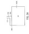
図3Aおよび3Bを参照すると、僅かに異なる周波数において共振するPIFA構成の概略図が示されている。図3Aにて示されたPIFAは第1の周波数にて共振し、図3Bに示されたPIFAは第2の周波数にて共振する。第1の共振周波数および第2の共振周波数は、僅かに異なる。たとえば、第1の周波数は約1900MHzであり、第2の周波数は約2100MHzである(PCS電話)。図3Aの放射素子302Aは、図3BのPIFAの放射素子302Bと同一である。これら2つのPIFAの間で共振周波数が異なるのは、コンタクト位置306および318が放射素子302Aおよび302Bにてそれぞれ、異なる場所に位置することに因る。 Referring to FIGS. 3A and 3B, a schematic diagram of a PIFA configuration that resonates at slightly different frequencies is shown. The PIFA shown in FIG. 3A resonates at the first frequency, and the PIFA shown in FIG. 3B resonates at the second frequency. The first resonance frequency and the second resonance frequency are slightly different. For example, the first frequency is about 1900 MHz and the second frequency is about 2100 MHz (PCS phone). The radiating
図3Cを参照すると、図3Aと3Bとが組み合わされて1つの広帯域PIFA構成になったPIFA構成が、概略的に図解されている。図3Aおよび3Bの2つのPIFA構造が組み合わされる場合、別個の放射素子302を必要とせずに、組み合わせPIFAの帯域幅が拡大される。接続線路310および312のセットだけを使用して、接続線路320を介してコンタクト位置306および318にて、接続線路312を放射素子302に結合することができる。アース接続線路310は、この新たなPIFA構造でも共通の接続線路となっている。放射素子302にて異なるコンタクト位置(306,318)を組み合わせることにより、多重共振、密接に結合された「スタガ同調」PIFA構造が実現される。このようにして実現されたPIFA構造は、より幅広い帯域幅を有し、製造してPCS等の無線システムにて使用するのに、よりクリティカルでなくなる。 Referring to FIG. 3C, a PIFA configuration is schematically illustrated in which FIGS. 3A and 3B are combined into a single wideband PIFA configuration. When the two PIFA structures of FIGS. 3A and 3B are combined, the bandwidth of the combined PIFA is increased without the need for a
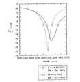
図4には、本発明の実施形態によるPIFAのパフォーマンス帯域幅の改善が、従来技術のPIFAと比較して示されている。この図は、(単に例として)PCSの適用のための従来のPIFAとともに、3つの供給点を有する本発明の改善されたPIFA構造のパフォーマンス改善がプロットされている。PCSの適用では、140MHzの帯域幅(1850〜1990MHz)が要求される。図4には、周波数を横軸として2つの入力反射係数S11の大きさがプロットされている。点線によって示されているのは、141.8MHzの帯域幅を有する標準的なPIFAの周波数帯域幅であり、実線は、198.4MHzを有する本発明の実施形態による3コンタクトPIFAの周波数帯域を示している。ここでは、本発明の実施形態において(帯域幅の設定が−10dBであると仮定して)、パフォーマンスの改善が約58MHzであることが示されている。 FIG. 4 illustrates the performance bandwidth improvement of a PIFA according to an embodiment of the present invention compared to a prior art PIFA. This figure plots the performance improvement of the improved PIFA structure of the present invention with three feed points along with a conventional PIFA for PCS application (as an example only). Application of PCS requires a bandwidth of 140 MHz (1850-1990 MHz). In FIG. 4, the magnitudes of the two input reflection coefficients S11 are plotted with the frequency as the horizontal axis. Shown by the dotted line is the frequency bandwidth of a standard PIFA with a bandwidth of 141.8 MHz, and the solid line shows the frequency band of a 3-contact PIFA according to an embodiment of the invention having 198.4 MHz. ing. Here, in an embodiment of the present invention (assuming the bandwidth setting is -10 dB), the performance improvement is shown to be about 58 MHz.
本発明は、本発明の実施例と関連して説明された。本発明によればシステムに対するパラメータは、とりわけ設計エンジニアが所望の適用のために該パラメータを指定および選択することによって変更することができる。さらに、ここに挙げられた思想に基づいて通常の知識を有する当業者が考案することもできる別の実施形態も、もちろん本発明の範囲内である。これは、従属請求項によって定義されている。本発明は、当業者にも理解できるように異なって、しかも同様に、変更および実施することができ、ここに挙げられた思想の利点を有する。 The invention has been described with reference to embodiments of the invention. In accordance with the present invention, parameters for the system can be altered, among other things, by design engineers specifying and selecting the parameters for the desired application. Furthermore, other embodiments that can be devised by those skilled in the art based on the concepts listed herein are of course within the scope of the invention. This is defined by the dependent claims. The present invention is different, as can be understood by those skilled in the art, and can be modified and implemented in the same way, and has the advantages of the ideas listed here.
Claims (26)
Translated fromJapanese第1の平面および第1のエリアを有するグランド面と、第2の平面および第2のエリアを有する放射素子とを有し、
該放射素子の第2の平面は、該グランド面の第1の平面と実質的に同一平面内に存在する形式のものにおいて、
第1の接続線路が、該グランド面の第1の縁部に結合されており、かつ第1のコンタクト位置にて該放射素子の第2の縁部に結合されており、
第2の接続線路が、第2のコンタクト位置および第3のコンタクト位置にて、該放射素子の第2の縁部に結合されていることを特徴とするアンテナ。An antenna,
A ground plane having a first plane and a first area; and a radiating element having a second plane and a second area;
The second plane of the radiating element is of a type that lies in substantially the same plane as the first plane of the ground plane;
A first connecting line is coupled to the first edge of the ground plane and is coupled to the second edge of the radiating element at a first contact location;
An antenna, wherein a second connection line is coupled to a second edge of the radiating element at a second contact position and a third contact position.
該放射素子は、該絶縁性基板上の他方の面に設けられている、請求項1記載のアンテナ。The ground surface is provided on one surface of the insulating substrate,
The antenna according to claim 1, wherein the radiating element is provided on the other surface of the insulating substrate.
第1の平面および第1のエリアを有するグランド面と、第2の平面および第2のエリアを有する放射素子とを有し、
該放射素子の第2の平面は、該グランド面の第1の平面と実質的に同一平面上にある形式のものにおいて、
第1の接続線路が、該グランド面の縁部および該放射素子の縁部に結合されており、
第2の接続線路が該放射素子の縁部に、該第1の接続線路が結合された一方の面で結合されていることを特徴とする平板状逆Fアンテナ。A flat inverted F antenna,
A ground plane having a first plane and a first area; and a radiating element having a second plane and a second area;
The second plane of the radiating element is of a type that is substantially coplanar with the first plane of the ground plane;
A first connecting line is coupled to an edge of the ground plane and an edge of the radiating element;
A flat inverted F antenna, wherein the second connection line is coupled to the edge of the radiating element on one side to which the first connection line is coupled.
第1の平面および第1の周縁部を有するグランド面と、第2の平面および第2の周縁部を有する放射素子とを備えており、
該グランド面の第1の周縁部上には、複数の第1の縁部が設けられており、
該放射素子の第2の周縁部上には、複数の第2の縁部が設けられており、
該放射素子の第2の平面は、該グランド面の第1の平面と実質的に同一平面上にある形式のものにおいて、
第1の接続線路が、前記複数の第1の縁部のうち第1の縁部と、前記複数の第2の縁部のうち第1の縁部とに結合されており、
第2の接続線路が、前記第1の接続線路の一方の側にて、前記複数の第2の縁部のうち該第1の縁部に結合されていることを特徴とする平板状逆Fアンテナ。A flat inverted F antenna,
A ground plane having a first plane and a first peripheral edge, and a radiating element having a second plane and a second peripheral edge,
A plurality of first edges are provided on the first peripheral edge of the ground surface,
A plurality of second edges are provided on the second peripheral edge of the radiating element,
The second plane of the radiating element is of a type that is substantially coplanar with the first plane of the ground plane;
A first connecting line is coupled to a first edge of the plurality of first edges and a first edge of the plurality of second edges;
A flat inverted F, wherein a second connection line is coupled to the first edge of the plurality of second edges on one side of the first connection line. antenna.
グランド面を第1の平面上に形成するステップと、
放射素子を第2の平面上に形成するステップとを有し、
前記第2の平面は、前記第1の平面と実質的に同一平面上に存在する形式の方法において、
第1の接続線路を該グランド面の第1の縁部に結合し、かつ第1のコンタクト位置にて該放射素子の第2の縁部に結合するステップと、
第2の接続線路を、第2のコンタクト位置および第3のコンタクト位置にて、該放射素子の第2の縁部に結合するステップとを有することを特徴とする製造方法。A method of manufacturing a flat inverted F antenna having a wide bandwidth,
Forming a ground plane on the first plane;
Forming a radiating element on a second plane;
In a method of the type, wherein the second plane is substantially coplanar with the first plane,
Coupling a first connecting line to a first edge of the ground plane and coupling to a second edge of the radiating element at a first contact location;
Coupling the second connecting line to the second edge of the radiating element at a second contact position and a third contact position.
第1の平面および第1のエリアを有するグランド面と、第2の平面および第2のエリアを有する放射素子とを有し、
該放射素子の第2の平面は、該グランド面の第1の平面と実質的に同一平面上に存在する形式のものにおいて、
第1の接続線路が該グランド面の第1の縁部に結合されており、かつ第1のコンタクト位置にて該放射素子の第2の縁部に結合されており、
第2の接続線路が、第2のコンタクト位置および第3のコンタクト位置にて該放射素子の第2の縁部に結合されており、
前記第1の接続線路および第2の接続線路は、所望のインピーダンスにて無線に整合されて結合されていることを特徴とする無線システム。A wireless system having a flat inverted F antenna (PIFA),
A ground plane having a first plane and a first area; and a radiating element having a second plane and a second area;
The second plane of the radiating element is of a type that is substantially coplanar with the first plane of the ground plane;
A first connecting line is coupled to the first edge of the ground plane, and is coupled to the second edge of the radiating element at a first contact location;
A second connecting line is coupled to the second edge of the radiating element at a second contact position and a third contact position;
The wireless system, wherein the first connection line and the second connection line are wirelessly matched and coupled with a desired impedance.
Applications Claiming Priority (2)
| Application Number | Priority Date | Filing Date | Title |
|---|---|---|---|
| US10/091,619US6882318B2 (en) | 2002-03-04 | 2002-03-04 | Broadband planar inverted F antenna |
| PCT/US2003/002884WO2003077355A2 (en) | 2002-03-04 | 2003-01-31 | Broadband planar inverted f antenna |
Publications (1)
| Publication Number | Publication Date |
|---|---|
| JP2006501699Atrue JP2006501699A (en) | 2006-01-12 |
Family
ID=27804129
Family Applications (1)
| Application Number | Title | Priority Date | Filing Date |
|---|---|---|---|
| JP2003575451APendingJP2006501699A (en) | 2002-03-04 | 2003-01-31 | Broadband flat inverted F antenna |
Country Status (7)
| Country | Link |
|---|---|
| US (2) | US6882318B2 (en) |
| EP (1) | EP1481443A4 (en) |
| JP (1) | JP2006501699A (en) |
| KR (2) | KR101006296B1 (en) |
| CN (1) | CN100459291C (en) |
| TW (1) | TWI223468B (en) |
| WO (1) | WO2003077355A2 (en) |
Families Citing this family (51)
| Publication number | Priority date | Publication date | Assignee | Title |
|---|---|---|---|---|
| US7190319B2 (en)* | 2001-10-29 | 2007-03-13 | Forster Ian J | Wave antenna wireless communication device and method |
| WO2003038747A2 (en)* | 2001-10-29 | 2003-05-08 | Marconi Intellectual Property (Us) Inc | Wave antenna wireless communication device |
| US6630910B2 (en) | 2001-10-29 | 2003-10-07 | Marconi Communications Inc. | Wave antenna wireless communication device and method |
| DE10231961B3 (en)* | 2002-07-15 | 2004-02-12 | Kathrein-Werke Kg | Low-profile dual or multi-band antenna, especially for motor vehicles |
| EP1522122A1 (en)* | 2002-07-15 | 2005-04-13 | Fractus S.A. | Notched-fed antenna |
| EP2273611B1 (en)* | 2002-12-22 | 2012-02-08 | Fractus, S.A. | Multi-band monopole antenna for a mobile communications device |
| US20060147742A1 (en)* | 2003-02-04 | 2006-07-06 | Akira Matsuda | Composite copper foil, method of production thereof and high frequency transmission circuit using said composite copper foil |
| US7055754B2 (en)* | 2003-11-03 | 2006-06-06 | Avery Dennison Corporation | Self-compensating antennas for substrates having differing dielectric constant values |
| US7501984B2 (en)* | 2003-11-04 | 2009-03-10 | Avery Dennison Corporation | RFID tag using a surface insensitive antenna structure |
| US7652636B2 (en)* | 2003-04-10 | 2010-01-26 | Avery Dennison Corporation | RFID devices having self-compensating antennas and conductive shields |
| KR100542830B1 (en)* | 2003-11-17 | 2006-01-20 | 한국전자통신연구원 | Broadband / Multiband Antennas with Floating Radiation Patches and / or Microelectronic Precision Instrument Switches |
| EP1709704A2 (en) | 2004-01-30 | 2006-10-11 | Fractus, S.A. | Multi-band monopole antennas for mobile communications devices |
| US7183976B2 (en)* | 2004-07-21 | 2007-02-27 | Mark Iv Industries Corp. | Compact inverted-F antenna |
| US7501955B2 (en)* | 2004-09-13 | 2009-03-10 | Avery Dennison Corporation | RFID device with content insensitivity and position insensitivity |
| TWI274439B (en)* | 2004-09-17 | 2007-02-21 | Asustek Comp Inc | Telecommunication device and plane antenna thereof |
| DE102005030384B3 (en)* | 2005-06-29 | 2006-11-02 | Siemens Ag | Antenna for e.g. radiotelephone, has conductive strip that has output base portion squeezed to conductive strip frame through support frame when conductive strip frame and support portion are installed in radiotelephone |
| TWM288014U (en)* | 2005-08-08 | 2006-02-21 | Wistron Neweb Corp | Multifrequency H antenna |
| US7324054B2 (en)* | 2005-09-29 | 2008-01-29 | Sony Ericsson Mobile Communications Ab | Multi-band PIFA |
| US7405701B2 (en)* | 2005-09-29 | 2008-07-29 | Sony Ericsson Mobile Communications Ab | Multi-band bent monopole antenna |
| US7408512B1 (en) | 2005-10-05 | 2008-08-05 | Sandie Corporation | Antenna with distributed strip and integrated electronic components |
| US7345647B1 (en) | 2005-10-05 | 2008-03-18 | Sandia Corporation | Antenna structure with distributed strip |
| US8067253B2 (en) | 2005-12-21 | 2011-11-29 | Avery Dennison Corporation | Electrical device and method of manufacturing electrical devices using film embossing techniques to embed integrated circuits into film |
| US9007275B2 (en) | 2006-06-08 | 2015-04-14 | Fractus, S.A. | Distributed antenna system robust to human body loading effects |
| CN101192702B (en)* | 2006-11-24 | 2012-07-18 | 鸿富锦精密工业(深圳)有限公司 | Double frequency antenna |
| TWI354397B (en)* | 2007-04-16 | 2011-12-11 | Asustek Comp Inc | Antenna structure |
| US7436365B1 (en)* | 2007-05-02 | 2008-10-14 | Motorola, Inc. | Communications assembly and antenna radiator assembly |
| TWI478437B (en)* | 2008-08-29 | 2015-03-21 | Chi Mei Comm Systems Inc | Antenna module and portable electronic device employing the same |
| US7986273B2 (en)* | 2008-10-30 | 2011-07-26 | Auden Techno Corp. | Multi-band monopole antenna with improved HAC performance |
| US8098205B2 (en)* | 2009-05-05 | 2012-01-17 | Flextronics Automotive Inc. | GPS, GSM, and wireless LAN antenna for vehicle applications |
| US7965239B2 (en)* | 2009-06-25 | 2011-06-21 | Cheng Uei Precision Industry Co., Ltd. | Antenna structure |
| EP2348578A1 (en)* | 2010-01-20 | 2011-07-27 | Insight sip sas | Improved antenna-in-package structure |
| FR2956214B1 (en)* | 2010-02-09 | 2012-02-24 | Commissariat Energie Atomique | LINEAR RESONATOR OF A HIGH FREQUENCY ANTENNA FOR NUCLEAR MAGNETIC RESONANCE IMAGING APPARATUS |
| US9160056B2 (en)* | 2010-04-01 | 2015-10-13 | Apple Inc. | Multiband antennas formed from bezel bands with gaps |
| US8432323B2 (en)* | 2010-07-30 | 2013-04-30 | Motorola Solutions, Inc. | Antenna integrated with a portable communication device |
| CN102570059A (en)* | 2010-12-31 | 2012-07-11 | 旭丽电子(广州)有限公司 | Independent multi-frequency antenna |
| TWI473349B (en)* | 2010-12-31 | 2015-02-11 | Lite On Electronics Guangzhou | Stand-alone multi-band antenna |
| US20120262355A1 (en)* | 2011-04-18 | 2012-10-18 | Ziming He | High gain low profile multi-band antenna for wireless communications |
| US20120262354A1 (en)* | 2011-04-18 | 2012-10-18 | Ziming He | High gain low profile multi-band antenna for wireless communications |
| TWI495192B (en)* | 2012-07-27 | 2015-08-01 | Askey Computer Corp | Multiband antenna |
| CN103117456B (en)* | 2013-02-20 | 2015-12-09 | 上海安费诺永亿通讯电子有限公司 | A kind of enhancing bandwidth reconfigurable antenna |
| US9166634B2 (en) | 2013-05-06 | 2015-10-20 | Apple Inc. | Electronic device with multiple antenna feeds and adjustable filter and matching circuitry |
| TWI619307B (en)* | 2013-05-16 | 2018-03-21 | 富智康(香港)有限公司 | Antenna assembly, wireless communication device and manufacturing method employing same |
| WO2015046937A1 (en)* | 2013-09-30 | 2015-04-02 | Samsung Electronics Co., Ltd. | Electronic device with pifa type antenna and wireless signal transmitting/receiving device thereof |
| KR102078101B1 (en) | 2013-09-30 | 2020-02-17 | 삼성전자 주식회사 | Electronic device having antenna of pifa type and apparatus for transmitting/receiving wireless signal thereof |
| US10128573B2 (en) | 2014-10-17 | 2018-11-13 | Wispry, Inc. | Tunable multiple-resonance antenna systems, devices, and methods for handsets operating in low LTE bands with wide duplex spacing |
| US10205241B2 (en) | 2016-05-05 | 2019-02-12 | Laird Technology, Inc. | Low profile omnidirectional antennas |
| TWM538255U (en)* | 2016-05-05 | 2017-03-11 | 雷爾德科技有限公司 | Low profile omnidirectional antennas |
| US10756419B2 (en)* | 2018-01-11 | 2020-08-25 | Savannah River Nuclear Solutions, Llc | Laser induced graphene/graphite antenna |
| TWI675506B (en)* | 2018-09-07 | 2019-10-21 | 啓碁科技股份有限公司 | Antenna structure |
| US20220223997A1 (en)* | 2021-01-13 | 2022-07-14 | Zebra Technologies Corporation | User-Installable Wireless Communications Module |
| CN216903338U (en)* | 2021-07-13 | 2022-07-05 | 荣耀终端有限公司 | Shrapnel connection structure and electronic equipment |
Citations (9)
| Publication number | Priority date | Publication date | Assignee | Title |
|---|---|---|---|---|
| JPH01295505A (en)* | 1988-02-23 | 1989-11-29 | Sanyo Electric Co Ltd | Antenna system |
| JPH06303018A (en)* | 1993-04-13 | 1994-10-28 | Matsushita Electric Ind Co Ltd | Printed antenna |
| JPH07131234A (en)* | 1993-11-02 | 1995-05-19 | Nippon Mektron Ltd | Biresonance antenna |
| JPH07226613A (en)* | 1994-02-09 | 1995-08-22 | Murata Mfg Co Ltd | Surface mounted type antenna |
| JPH08195609A (en)* | 1995-01-18 | 1996-07-30 | Matsushita Electric Ind Co Ltd | Inverted F antenna with built-in portable radio |
| JPH09252214A (en)* | 1996-03-15 | 1997-09-22 | Kokusai Electric Co Ltd | Inverted F antenna |
| JPH1056320A (en)* | 1996-03-13 | 1998-02-24 | Ascom Tech Ag | Flat three-dimensional antenna |
| WO2001003238A1 (en)* | 1999-06-29 | 2001-01-11 | Siemens Aktiengesellschaft | Integrable dual-band antenna |
| JP2001345629A (en)* | 2000-06-01 | 2001-12-14 | Matsushita Electric Ind Co Ltd | Antenna device |
Family Cites Families (20)
| Publication number | Priority date | Publication date | Assignee | Title |
|---|---|---|---|---|
| US6281850B1 (en) | 1996-02-16 | 2001-08-28 | Intermec Ip Corp. | Broadband multiple element antenna system |
| FI113212B (en)* | 1997-07-08 | 2004-03-15 | Nokia Corp | Dual resonant antenna design for multiple frequency ranges |
| AU8365998A (en)* | 1997-07-09 | 1999-02-08 | Allgon Ab | Trap microstrip pifa |
| FR2772519B1 (en)* | 1997-12-11 | 2000-01-14 | Alsthom Cge Alcatel | ANTENNA REALIZED ACCORDING TO MICRO-TAPE TECHNIQUE AND DEVICE INCLUDING THIS ANTENNA |
| KR20010023541A (en)* | 1998-07-02 | 2001-03-26 | 마츠시타 덴끼 산교 가부시키가이샤 | Antenna unit, communication system and digital television receiver |
| US6140967A (en) | 1998-08-27 | 2000-10-31 | Lucent Technologies Inc. | Electronically variable power control in microstrip line fed antenna systems |
| KR20010075127A (en) | 1998-09-16 | 2001-08-09 | 칼 하인쯔 호르닝어 | Antenna which can be operated in several frequency bands |
| FI105421B (en)* | 1999-01-05 | 2000-08-15 | Filtronic Lk Oy | Planes two frequency antenna and radio device equipped with a planar antenna |
| US6204826B1 (en) | 1999-07-22 | 2001-03-20 | Ericsson Inc. | Flat dual frequency band antennas for wireless communicators |
| WO2001013464A1 (en)* | 1999-08-18 | 2001-02-22 | Ericsson, Inc. | A dual band bowtie/meander antenna |
| WO2001017064A1 (en) | 1999-08-27 | 2001-03-08 | Antennas America, Inc. | Compact planar inverted f antenna |
| WO2001029927A1 (en) | 1999-10-15 | 2001-04-26 | Siemens Aktiengesellschaft | Switchable antenna |
| JP2001185938A (en) | 1999-12-27 | 2001-07-06 | Mitsubishi Electric Corp | Dual-frequency antenna, multi-frequency antenna, and dual-frequency or multi-frequency array antenna |
| FI113911B (en)* | 1999-12-30 | 2004-06-30 | Nokia Corp | Method for coupling a signal and antenna structure |
| SE518813C2 (en) | 2000-04-18 | 2002-11-26 | Ericsson Telefon Ab L M | Multi-band antenna and portable telecommunication apparatus including such an antenna |
| JP2002064324A (en)* | 2000-08-23 | 2002-02-28 | Matsushita Electric Ind Co Ltd | Antenna device |
| TW529203B (en) | 2000-11-14 | 2003-04-21 | Ind Tech Res Inst | Planar antenna device having slit |
| US6459413B1 (en) | 2001-01-10 | 2002-10-01 | Industrial Technology Research Institute | Multi-frequency band antenna |
| US6798383B2 (en)* | 2001-02-05 | 2004-09-28 | Sony Corporation | Low profile small antenna and constructing method therefor |
| US6380903B1 (en)* | 2001-02-16 | 2002-04-30 | Telefonaktiebolaget L.M. Ericsson | Antenna systems including internal planar inverted-F antennas coupled with retractable antennas and wireless communicators incorporating same |
- 2002
- 2002-03-04USUS10/091,619patent/US6882318B2/ennot_activeExpired - Fee Related
- 2002-03-27USUS10/108,059patent/US6856285B2/ennot_activeExpired - Fee Related
- 2003
- 2003-01-31JPJP2003575451Apatent/JP2006501699A/enactivePending
- 2003-01-31CNCNB038051419Apatent/CN100459291C/ennot_activeExpired - Fee Related
- 2003-01-31WOPCT/US2003/002884patent/WO2003077355A2/enactiveApplication Filing
- 2003-01-31KRKR1020047013777Apatent/KR101006296B1/ennot_activeExpired - Fee Related
- 2003-01-31EPEP03708912Apatent/EP1481443A4/ennot_activeWithdrawn
- 2003-01-31KRKR10-2004-7009688Apatent/KR20040083475A/ennot_activeWithdrawn
- 2003-02-25TWTW092103893Apatent/TWI223468B/ennot_activeIP Right Cessation
Patent Citations (9)
| Publication number | Priority date | Publication date | Assignee | Title |
|---|---|---|---|---|
| JPH01295505A (en)* | 1988-02-23 | 1989-11-29 | Sanyo Electric Co Ltd | Antenna system |
| JPH06303018A (en)* | 1993-04-13 | 1994-10-28 | Matsushita Electric Ind Co Ltd | Printed antenna |
| JPH07131234A (en)* | 1993-11-02 | 1995-05-19 | Nippon Mektron Ltd | Biresonance antenna |
| JPH07226613A (en)* | 1994-02-09 | 1995-08-22 | Murata Mfg Co Ltd | Surface mounted type antenna |
| JPH08195609A (en)* | 1995-01-18 | 1996-07-30 | Matsushita Electric Ind Co Ltd | Inverted F antenna with built-in portable radio |
| JPH1056320A (en)* | 1996-03-13 | 1998-02-24 | Ascom Tech Ag | Flat three-dimensional antenna |
| JPH09252214A (en)* | 1996-03-15 | 1997-09-22 | Kokusai Electric Co Ltd | Inverted F antenna |
| WO2001003238A1 (en)* | 1999-06-29 | 2001-01-11 | Siemens Aktiengesellschaft | Integrable dual-band antenna |
| JP2001345629A (en)* | 2000-06-01 | 2001-12-14 | Matsushita Electric Ind Co Ltd | Antenna device |
Also Published As
| Publication number | Publication date |
|---|---|
| WO2003077355A3 (en) | 2004-06-24 |
| TWI223468B (en) | 2004-11-01 |
| US20030184482A1 (en) | 2003-10-02 |
| EP1481443A4 (en) | 2009-06-17 |
| CN100459291C (en) | 2009-02-04 |
| WO2003077355A2 (en) | 2003-09-18 |
| KR20040088577A (en) | 2004-10-16 |
| TW200304247A (en) | 2003-09-16 |
| KR20040083475A (en) | 2004-10-02 |
| US6882318B2 (en) | 2005-04-19 |
| CN1639909A (en) | 2005-07-13 |
| EP1481443A2 (en) | 2004-12-01 |
| US20030164798A1 (en) | 2003-09-04 |
| US6856285B2 (en) | 2005-02-15 |
| KR101006296B1 (en) | 2011-01-06 |
Similar Documents
| Publication | Publication Date | Title |
|---|---|---|
| JP2006501699A (en) | Broadband flat inverted F antenna | |
| JP4394278B2 (en) | Antenna with two active radiators | |
| JP4259760B2 (en) | One plane dual strip antenna | |
| US6373436B1 (en) | Dual strip antenna with periodic mesh pattern | |
| US6429819B1 (en) | Dual band patch bowtie slot antenna structure | |
| TW200400665A (en) | Single piece twin folded dipole antenna | |
| CN101345331A (en) | Electronic device and manufacturing method thereof | |
| JP2003174317A (en) | Multi-band patch antenna and skeleton slot radiator | |
| WO2022083276A1 (en) | Antenna array assembly and electronic device | |
| WO2019223318A1 (en) | Indoor base station and pifa antenna thereof | |
| CN207116688U (en) | Dual frequency high gain omnidirectional antenna | |
| JP2005519509A (en) | Multiband PIF antenna having meander structure | |
| KR100449857B1 (en) | Wideband Printed Dipole Antenna | |
| JP3735582B2 (en) | Multilayer dielectric antenna | |
| CN120601125A (en) | Antenna, electronic device and vehicle | |
| CN101483269A (en) | Antenna applied to wireless wide area network | |
| MXPA00008248A (en) | Antenna with two active radiators | |
| CN1848524A (en) | Antenna device, manufacturing method thereof, and mobile phone and global positioning dual-use system |
Legal Events
| Date | Code | Title | Description |
|---|---|---|---|
| A621 | Written request for application examination | Free format text:JAPANESE INTERMEDIATE CODE: A621 Effective date:20060130 | |
| A131 | Notification of reasons for refusal | Free format text:JAPANESE INTERMEDIATE CODE: A131 Effective date:20071004 | |
| A601 | Written request for extension of time | Free format text:JAPANESE INTERMEDIATE CODE: A601 Effective date:20071228 | |
| A602 | Written permission of extension of time | Free format text:JAPANESE INTERMEDIATE CODE: A602 Effective date:20080110 | |
| A601 | Written request for extension of time | Free format text:JAPANESE INTERMEDIATE CODE: A601 Effective date:20080204 | |
| A602 | Written permission of extension of time | Free format text:JAPANESE INTERMEDIATE CODE: A602 Effective date:20080212 | |
| A601 | Written request for extension of time | Free format text:JAPANESE INTERMEDIATE CODE: A601 Effective date:20080304 | |
| A602 | Written permission of extension of time | Free format text:JAPANESE INTERMEDIATE CODE: A602 Effective date:20080312 | |
| A521 | Request for written amendment filed | Free format text:JAPANESE INTERMEDIATE CODE: A523 Effective date:20080402 | |
| A131 | Notification of reasons for refusal | Free format text:JAPANESE INTERMEDIATE CODE: A131 Effective date:20080424 | |
| A521 | Request for written amendment filed | Free format text:JAPANESE INTERMEDIATE CODE: A523 Effective date:20080718 | |
| A131 | Notification of reasons for refusal | Free format text:JAPANESE INTERMEDIATE CODE: A131 Effective date:20080820 | |
| A601 | Written request for extension of time | Free format text:JAPANESE INTERMEDIATE CODE: A601 Effective date:20081119 | |
| A602 | Written permission of extension of time | Free format text:JAPANESE INTERMEDIATE CODE: A602 Effective date:20081127 | |
| A521 | Request for written amendment filed | Free format text:JAPANESE INTERMEDIATE CODE: A523 Effective date:20081222 | |
| A02 | Decision of refusal | Free format text:JAPANESE INTERMEDIATE CODE: A02 Effective date:20090130 | |
| A521 | Request for written amendment filed | Free format text:JAPANESE INTERMEDIATE CODE: A523 Effective date:20090430 | |
| A711 | Notification of change in applicant | Free format text:JAPANESE INTERMEDIATE CODE: A711 Effective date:20090610 | |
| A521 | Request for written amendment filed | Free format text:JAPANESE INTERMEDIATE CODE: A821 Effective date:20090610 | |
| A911 | Transfer to examiner for re-examination before appeal (zenchi) | Free format text:JAPANESE INTERMEDIATE CODE: A911 Effective date:20090717 | |
| A912 | Re-examination (zenchi) completed and case transferred to appeal board | Free format text:JAPANESE INTERMEDIATE CODE: A912 Effective date:20090807 | |
| RD04 | Notification of resignation of power of attorney | Free format text:JAPANESE INTERMEDIATE CODE: A7424 Effective date:20101227 | |
| RD04 | Notification of resignation of power of attorney | Free format text:JAPANESE INTERMEDIATE CODE: A7424 Effective date:20101228 | |
| A601 | Written request for extension of time | Free format text:JAPANESE INTERMEDIATE CODE: A601 Effective date:20110105 | |
| A602 | Written permission of extension of time | Free format text:JAPANESE INTERMEDIATE CODE: A602 Effective date:20110111 | |
| A601 | Written request for extension of time | Free format text:JAPANESE INTERMEDIATE CODE: A601 Effective date:20110207 | |
| A602 | Written permission of extension of time | Free format text:JAPANESE INTERMEDIATE CODE: A602 Effective date:20110210 | |
| A601 | Written request for extension of time | Free format text:JAPANESE INTERMEDIATE CODE: A601 Effective date:20110308 | |
| A602 | Written permission of extension of time | Free format text:JAPANESE INTERMEDIATE CODE: A602 Effective date:20110315 | |
| A601 | Written request for extension of time | Free format text:JAPANESE INTERMEDIATE CODE: A601 Effective date:20111110 | |
| A602 | Written permission of extension of time | Free format text:JAPANESE INTERMEDIATE CODE: A602 Effective date:20111122 | |
| A601 | Written request for extension of time | Free format text:JAPANESE INTERMEDIATE CODE: A601 Effective date:20111212 | |
| A602 | Written permission of extension of time | Free format text:JAPANESE INTERMEDIATE CODE: A602 Effective date:20111215 | |
| A601 | Written request for extension of time | Free format text:JAPANESE INTERMEDIATE CODE: A601 Effective date:20120110 | |
| A602 | Written permission of extension of time | Free format text:JAPANESE INTERMEDIATE CODE: A602 Effective date:20120113 | |
| A521 | Request for written amendment filed | Free format text:JAPANESE INTERMEDIATE CODE: A523 Effective date:20120207 |