JP2006344849A - Thin film transistor - Google Patents
Thin film transistorDownload PDFInfo
- Publication number
- JP2006344849A JP2006344849AJP2005170348AJP2005170348AJP2006344849AJP 2006344849 AJP2006344849 AJP 2006344849AJP 2005170348 AJP2005170348 AJP 2005170348AJP 2005170348 AJP2005170348 AJP 2005170348AJP 2006344849 AJP2006344849 AJP 2006344849A
- Authority
- JP
- Japan
- Prior art keywords
- thin film
- electrode
- semiconductor thin
- film
- ohmic contact
- Prior art date
- Legal status (The legal status is an assumption and is not a legal conclusion. Google has not performed a legal analysis and makes no representation as to the accuracy of the status listed.)
- Pending
Links
Images


Classifications
- H—ELECTRICITY
- H10—SEMICONDUCTOR DEVICES; ELECTRIC SOLID-STATE DEVICES NOT OTHERWISE PROVIDED FOR
- H10D—INORGANIC ELECTRIC SEMICONDUCTOR DEVICES
- H10D30/00—Field-effect transistors [FET]
- H10D30/60—Insulated-gate field-effect transistors [IGFET]
- H10D30/67—Thin-film transistors [TFT]
- H10D30/674—Thin-film transistors [TFT] characterised by the active materials
- H10D30/6755—Oxide semiconductors, e.g. zinc oxide, copper aluminium oxide or cadmium stannate
- H—ELECTRICITY
- H10—SEMICONDUCTOR DEVICES; ELECTRIC SOLID-STATE DEVICES NOT OTHERWISE PROVIDED FOR
- H10D—INORGANIC ELECTRIC SEMICONDUCTOR DEVICES
- H10D30/00—Field-effect transistors [FET]
- H10D30/60—Insulated-gate field-effect transistors [IGFET]
- H10D30/67—Thin-film transistors [TFT]
- H10D30/6729—Thin-film transistors [TFT] characterised by the electrodes
- H10D30/6737—Thin-film transistors [TFT] characterised by the electrodes characterised by the electrode materials
- H—ELECTRICITY
- H10—SEMICONDUCTOR DEVICES; ELECTRIC SOLID-STATE DEVICES NOT OTHERWISE PROVIDED FOR
- H10D—INORGANIC ELECTRIC SEMICONDUCTOR DEVICES
- H10D86/00—Integrated devices formed in or on insulating or conducting substrates, e.g. formed in silicon-on-insulator [SOI] substrates or on stainless steel or glass substrates
- H10D86/40—Integrated devices formed in or on insulating or conducting substrates, e.g. formed in silicon-on-insulator [SOI] substrates or on stainless steel or glass substrates characterised by multiple TFTs
- H10D86/421—Integrated devices formed in or on insulating or conducting substrates, e.g. formed in silicon-on-insulator [SOI] substrates or on stainless steel or glass substrates characterised by multiple TFTs having a particular composition, shape or crystalline structure of the active layer
- H10D86/423—Integrated devices formed in or on insulating or conducting substrates, e.g. formed in silicon-on-insulator [SOI] substrates or on stainless steel or glass substrates characterised by multiple TFTs having a particular composition, shape or crystalline structure of the active layer comprising semiconductor materials not belonging to the Group IV, e.g. InGaZnO
- H—ELECTRICITY
- H10—SEMICONDUCTOR DEVICES; ELECTRIC SOLID-STATE DEVICES NOT OTHERWISE PROVIDED FOR
- H10D—INORGANIC ELECTRIC SEMICONDUCTOR DEVICES
- H10D86/00—Integrated devices formed in or on insulating or conducting substrates, e.g. formed in silicon-on-insulator [SOI] substrates or on stainless steel or glass substrates
- H10D86/40—Integrated devices formed in or on insulating or conducting substrates, e.g. formed in silicon-on-insulator [SOI] substrates or on stainless steel or glass substrates characterised by multiple TFTs
- H10D86/60—Integrated devices formed in or on insulating or conducting substrates, e.g. formed in silicon-on-insulator [SOI] substrates or on stainless steel or glass substrates characterised by multiple TFTs wherein the TFTs are in active matrices
- H—ELECTRICITY
- H10—SEMICONDUCTOR DEVICES; ELECTRIC SOLID-STATE DEVICES NOT OTHERWISE PROVIDED FOR
- H10D—INORGANIC ELECTRIC SEMICONDUCTOR DEVICES
- H10D99/00—Subject matter not provided for in other groups of this subclass
- G—PHYSICS
- G02—OPTICS
- G02F—OPTICAL DEVICES OR ARRANGEMENTS FOR THE CONTROL OF LIGHT BY MODIFICATION OF THE OPTICAL PROPERTIES OF THE MEDIA OF THE ELEMENTS INVOLVED THEREIN; NON-LINEAR OPTICS; FREQUENCY-CHANGING OF LIGHT; OPTICAL LOGIC ELEMENTS; OPTICAL ANALOGUE/DIGITAL CONVERTERS
- G02F1/00—Devices or arrangements for the control of the intensity, colour, phase, polarisation or direction of light arriving from an independent light source, e.g. switching, gating or modulating; Non-linear optics
- G02F1/01—Devices or arrangements for the control of the intensity, colour, phase, polarisation or direction of light arriving from an independent light source, e.g. switching, gating or modulating; Non-linear optics for the control of the intensity, phase, polarisation or colour
- G02F1/13—Devices or arrangements for the control of the intensity, colour, phase, polarisation or direction of light arriving from an independent light source, e.g. switching, gating or modulating; Non-linear optics for the control of the intensity, phase, polarisation or colour based on liquid crystals, e.g. single liquid crystal display cells
- G02F1/133—Constructional arrangements; Operation of liquid crystal cells; Circuit arrangements
- G02F1/136—Liquid crystal cells structurally associated with a semi-conducting layer or substrate, e.g. cells forming part of an integrated circuit
- G02F1/1362—Active matrix addressed cells
- G02F1/1368—Active matrix addressed cells in which the switching element is a three-electrode device
Landscapes
- Physics & Mathematics (AREA)
- Nonlinear Science (AREA)
- Mathematical Physics (AREA)
- Engineering & Computer Science (AREA)
- Chemical & Material Sciences (AREA)
- Crystallography & Structural Chemistry (AREA)
- Microelectronics & Electronic Packaging (AREA)
- General Physics & Mathematics (AREA)
- Optics & Photonics (AREA)
- Thin Film Transistor (AREA)
- Liquid Crystal (AREA)
- Dram (AREA)
- Electrodes Of Semiconductors (AREA)
Abstract
Translated fromJapaneseDescription
Translated fromJapaneseこの発明は薄膜トランジスタに関する。 The present invention relates to a thin film transistor.
例えば、アクティブマトリクス型液晶表示装置のスイッチング素子として用いられる薄膜トランジスタには、絶縁基板の上面にゲート電極が設けられ、ゲート電極を含む絶縁基板の上面にゲート絶縁膜が設けられ、ゲート電極上におけるゲート絶縁膜の上面に真性アモルファスシリコンからなる半導体薄膜が設けられ、半導体薄膜の上面中央部にチャネル保護膜が設けられ、チャネル保護膜の上面両側およびその両側における半導体薄膜の上面にn型アモルファスシリコンからなるオーミックコンタクト層が設けられ、各オーミックコンタクト層の上面にソース・ドレイン電極が設けられたものがある(例えば、特許文献1参照)。 For example, in a thin film transistor used as a switching element of an active matrix liquid crystal display device, a gate electrode is provided on the upper surface of an insulating substrate, a gate insulating film is provided on the upper surface of the insulating substrate including the gate electrode, and a gate on the gate electrode is provided. A semiconductor thin film made of intrinsic amorphous silicon is provided on the upper surface of the insulating film, a channel protective film is provided in the center of the upper surface of the semiconductor thin film, and n-type amorphous silicon is formed on both sides of the upper surface of the channel protective film and on the upper surface of the semiconductor thin film on both sides. The ohmic contact layer is formed, and the source / drain electrode is provided on the upper surface of each ohmic contact layer (see, for example, Patent Document 1).
ところで、最近では、アモルファスシリコンの代わりに、それよりも高い移動度が得られることから、酸化亜鉛(ZnO)を用いることが考えられている。このような酸化亜鉛を用いた薄膜トランジスタの製造方法としては、例えば、ゲート絶縁膜上に真性酸化亜鉛からなる半導体薄膜形成用層を成膜し、半導体薄膜形成用層の上面に窒化シリコンからなるチャネル保護膜をパターン形成し、チャネル保護膜を含む半導体薄膜形成用層の上面にn型酸化亜鉛からなるオーミックコンタクト層形成用層を成膜し、オーミックコンタクト層形成用層および半導体薄膜形成用層を連続してパターニングして、デバイスエリアにオーミックコンタクト層および半導体薄膜を形成し、各オーミックコンタクト層の上面にソース・ドレイン電極をパターン形成することが考えられる。 Recently, instead of amorphous silicon, higher mobility can be obtained, and therefore it is considered to use zinc oxide (ZnO). As a method for manufacturing such a thin film transistor using zinc oxide, for example, a semiconductor thin film forming layer made of intrinsic zinc oxide is formed on a gate insulating film, and a channel made of silicon nitride is formed on the upper surface of the semiconductor thin film forming layer. A protective film is patterned, an ohmic contact layer forming layer made of n-type zinc oxide is formed on the upper surface of the semiconductor thin film forming layer including the channel protective film, and the ohmic contact layer forming layer and the semiconductor thin film forming layer are formed It is conceivable to perform continuous patterning to form an ohmic contact layer and a semiconductor thin film in the device area, and pattern the source / drain electrodes on the upper surface of each ohmic contact layer.
しかしながら、上記製造方法では、酸化亜鉛が酸にもアルカリにも溶けやすく、エッチング耐性が極めて低いため、デバイスエリアに形成された酸化亜鉛からなる半導体薄膜およびオーミックコンタクト層に後工程で比較的大きなサイドエッチングが生じ、加工精度が悪くなってしまうということが分かった。 However, in the above manufacturing method, since zinc oxide is easily dissolved in both acid and alkali, and etching resistance is extremely low, a relatively large side is formed in the semiconductor thin film and ohmic contact layer made of zinc oxide formed in the device area in a later step. It has been found that etching occurs and processing accuracy deteriorates.
そこで、この発明は、加工精度を良くすることができる薄膜トランジスタを提供することを目的とする。 Accordingly, an object of the present invention is to provide a thin film transistor capable of improving processing accuracy.
この発明は、上記目的を達成するため、真性酸化亜鉛からなる半導体薄膜と、前記半導体薄膜の上面全体に設けられた保護膜と、前記保護膜上に設けられた絶縁膜と、前記半導体薄膜上における前記絶縁膜上に設けられたゲート電極と、前記半導体薄膜下に該半導体薄膜に電気的に接続されて設けられたソース電極およびドレイン電極とを有することを特徴とするものである。 In order to achieve the above object, the present invention provides a semiconductor thin film made of intrinsic zinc oxide, a protective film provided on the entire upper surface of the semiconductor thin film, an insulating film provided on the protective film, and the semiconductor thin film A gate electrode provided on the insulating film, and a source electrode and a drain electrode provided below the semiconductor thin film and electrically connected to the semiconductor thin film.
この発明によれば、真性酸化亜鉛からなる半導体薄膜の上面全体に保護膜を設けることにより、すなわち、真性酸化亜鉛からなる半導体薄膜形成用膜の上面に保護膜を形成するためのレジストパターンを剥離するとき、保護膜下の半導体薄膜形成用膜を保護膜で保護し、次いで保護膜をマスクとして半導体薄膜形成用膜をエッチングして保護膜下に半導体薄膜を形成し、そして半導体薄膜の上面全体に保護膜をそのまま残すことにより、加工精度を良くすることができる。 According to the present invention, the protective film is provided on the entire upper surface of the semiconductor thin film made of intrinsic zinc oxide, that is, the resist pattern for forming the protective film on the upper surface of the semiconductor thin film forming film made of intrinsic zinc oxide is peeled off. When the semiconductor thin film forming film under the protective film is protected with the protective film, the semiconductor thin film forming film is then etched using the protective film as a mask to form the semiconductor thin film under the protective film, and the entire upper surface of the semiconductor thin film The processing accuracy can be improved by leaving the protective film as it is.
(第1実施形態)
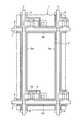
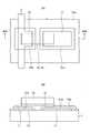
図1はこの発明の第1実施形態としての薄膜トランジスタを備えた液晶表示装置の要部の透過平面図を示し、図2(A)は図1の一部の拡大透過平面図を示し、図2(B)は図2(A)のIIB−IIB線に沿う断面図を示す。この液晶表示装置はガラス基板1を備えている。(First embodiment)
FIG. 1 shows a transmission plan view of a main part of a liquid crystal display device having a thin film transistor as a first embodiment of the present invention, FIG. 2 (A) shows a partially enlarged transmission plan view of FIG. (B) is a cross-sectional view taken along IIB -IIB line in FIG. 2 (a). The liquid crystal display device includes a
まず、図1を参照して説明する。ガラス基板1の上面側には走査ライン2およびデータライン3がマトリクス状に設けられ、両ライン2、3で囲まれた領域内には画素電極4が薄膜トランジスタ5を介して走査ライン2およびデータライン3に接続されて設けられ、さらに格子状の補助容量電極6が走査ライン2およびデータライン3と平行して設けられている。ここで、図1を含む図面全体において、その平面構成を明確にする目的で、画素電極4の縁部に斜めの短い実線のハッチングが記入されている。 First, a description will be given with reference to FIG. A
画素電極4の図1における左下角部は切り欠かれ、この切り欠かれた領域に薄膜トランジスタ5の主要部が配置されている。画素電極4の全周辺部は、その周囲に配置された格子状の補助容量電極6と重ね合わされている。格子状の補助容量電極6は、データライン3と重ね合わされた部分を含む第1の補助容量電極部6aと、走査ライン2と重ね合わされた部分を含む第2の補助容量電極部6bと、薄膜トランジスタ5の主要部と重ね合わされた部分を含む第3の補助容量電極部6cとからなっている。この場合、後で説明するが、補助容量電極6は走査ライン2と別の層上に設けられ、且つ、そのうちの特に第1の補助容量電極部6aは、厚さ方向において、すなわち、図1における紙面垂直方向において、データライン3と画素電極4との間にそれぞれ絶縁膜を介して設けられている。 The lower left corner of the
そして、第1の補助容量電極部6aの幅はデータライン3の幅よりもある程度大きくなっている。これにより、第1の補助容量電極部6aは、データライン3と直交する方向の位置ずれがあっても、データライン3が画素電極4と直接対向しないように、データライン3を確実に覆うようになっている。また、第1の補助容量電極部6aはデータライン3の配置領域のほぼ全域に亘って配置されている。これにより、第1の補助容量電極部6aは、画素電極4に対し、データライン3と平行な方向の位置ずれがあっても、画素電極4の左右辺部と確実に重なり、当該方向の位置合わせずれによる補助容量の変動を確実に防止するようになっている。 The width of the first auxiliary
第2の補助容量電極部6bの幅は走査ライン2の幅よりもある程度大きくなっている。これにより、第2の補助容量電極部6bは、走査ライン2と直交する方向の位置ずれがあっても、走査ライン2を確実に覆うようになっている。また、第2の補助容量電極部6bは走査ライン2の配置領域のほぼ全域に亘って配置されている。これにより、第2の補助容量電極部6bは、画素電極4に対し、走査ライン2と平行な方向の位置ずれがあっても、画素電極4の上下辺部と確実に重なり、当該方向の位置合わせずれによる補助容量の変動を確実に防止するようになっている。 The width of the second auxiliary
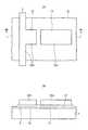
次に、この液晶表示装置の具体的な構造について、図2(A)、(B)を参照して説明する。ガラス基板1の上面の各所定の箇所にはアルミニウム、クロム、ITOなどからなるソース電極11、ドレイン電極12および該ドレイン電極12に接続されたデータライン3が設けられている。ソース電極11の上面のドレイン電極12側にはn型酸化亜鉛からなる一方のオーミックコンタクト層13が設けられている。データライン3の一部を含むドレイン電極12の上面のソース電極11側にはn型酸化亜鉛からなる他方のオーミックコンタクト層14が設けられている。この場合、オーミックコンタクト層13、14の互いに対向する端面13a、14aはソース電極11およびドレイン電極12の互いに対向する端面11a、12aと同一形状となっている。なお、ここで、酸化亜鉛とは、ZnOのみならず、ZnOの他、Mg、Cd等を含むZnO系全体を意味するものである。 Next, a specific structure of the liquid crystal display device will be described with reference to FIGS. A
2つのオーミックコンタクト層13、14の上面全体およびその間のガラス基板1の上面には真性酸化亜鉛からなる半導体薄膜15が設けられている。半導体薄膜15の上面全体には窒化シリコンからなる保護膜16が設けられている。ここで、半導体薄膜15と保護膜16とは、図2(A)に図示される如く、平面形状が同一である。また、2つのオーミックコンタクト層13、14は、互いに対向する端面13a、14aを除く周端面が半導体薄膜15および保護膜16の周端面と同一形状となっている。そして、2つのオーミックコンタクト層13、14間の端面13aと14aの間隔がチャネル長Lとなっており、オーミックコンタクト層13、14のチャネル長Lに直交する方向の寸法がチャネル幅Wとなっている。 A semiconductor
保護膜16、ソース電極11およびデータライン3を含むガラス基板1の上面には窒化シリコンからなる絶縁膜17が設けられている。絶縁膜17の上面の所定の箇所にはアルミニウム、クロム、ITOなどからなるゲート電極18および該ゲート電極18に接続された走査ライン2が設けられている。 An
ここで、ソース電極11、ドレイン電極12、オーミックコンタクト層13、14、半導体薄膜15、保護膜16、絶縁膜17およびゲート電極18により、トツプゲート構造の薄膜トランジスタ5が構成されている。この場合、薄膜トランジスタ5のゲート絶縁膜は、保護膜16および絶縁膜17によって形成されている。 Here, the
ゲート電極18および走査ライン2を含む絶縁膜17の上面には窒化シリコンからなる上層絶縁膜19が設けられている。上層絶縁膜19の上面の所定の箇所にはアルミニウム、クロムなどの遮光性金属からなるほぼ格子状の補助容量電極6が設けられている。補助容量電極6を含む上層絶縁膜19の上面には窒化シリコンからなるオーバーコート膜20が設けられている。ソース電極11の所定の箇所に対応する部分におけるオーバーコート膜20、上層絶縁膜19および絶縁膜17にはコンタクトホール21が設けられている。オーバーコート膜20の上面の所定の箇所にはITOなどの透明導電材料からなる画素電極4がコンタクトホール21を介してソース電極11に接続されて設けられている。 An upper
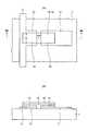
次に、この液晶表示装置における薄膜トランジスタ5の部分の製造方法の一例について説明する。まず、図3(A)、(B)に示すように、ガラス基板1の上面の各所定の箇所に、スパッタ法により成膜されたアルミニウム、クロム、ITOなどからなる金属膜をフォトリソグラフィ法によりパターニングすることにより、ソース電極11、ドレイン電極12および該ドレイン電極12に接続されたデータライン3を形成する。 Next, an example of a method for manufacturing the
次に、ソース電極11、ドレイン電極12およびデータライン3を含むガラス基板1の上面に、対向ターゲット方式のスパッタリングにより、n型酸化亜鉛からなる第1のオーミックコンタクト層形成用層31を成膜する。この場合、インジウムおよび亜鉛をターゲットとして、若しくは、ガリウムおよび亜鉛をターゲットとして、酸素ガスを用いた反応性スパッタリングにより形成することができる。また、インジウム−亜鉛酸化物(InZnO)やガリウム−亜鉛酸化物(GaZnO)をターゲットとして形成してもよい。 Next, a first ohmic contact
次に、第1のオーミックコンタクト層形成用層31の上面の各所定の箇所に、裏面露光(ガラス基板1の下面側からの露光)を含むフォトリソグラフィ法により、レジストパターン32a、32bを形成する。この場合、裏面露光であるため、一方のレジストパターン32aはソース電極11上に形成され、他方のレジストパターン32bはドレイン電極12およびデータライン3上に形成される。 Next,
次に、レジストパターン32a、32bをマスクとして、第1のオーミックコンタクト層形成用層31をエッチングすると、図4(A)、(B)に示すように、レジストパターン32a、32b下に第2のオーミックコンタクト層形成用層31a、31bが形成される。この場合、n型酸化亜鉛からなる第1のオーミックコンタクト層形成用層31のエッチング液としては、アルカリ水溶液を用いる。例えば、水酸化ナトリウム(NaOH)30wt%未満水溶液、好ましくは2〜10wt%水溶液を用いる。エッチング液の温度は、5〜40℃、好ましくは室温(22〜23℃)とする。 Next, when the first ohmic contact
そして、エッチング液として水酸化ナトリウム(NaOH)5wt%水溶液(温度は室温(22〜23℃))を用いたところ、エッチング速度は約80nm/分であった。ところで、エッチング速度は、加工の制御性を考慮した場合、余り大きいと膜厚や密度などのばらつきの要因のためエッチング終了の制御が難しく、勿論、小さすぎれば生産性が低下する。そこで、エッチング速度は、一般的に、100〜200nm/分程度が好ましいと言われている。エッチング速度が約80nm/分の水酸化ナトリウム(NaOH)5wt%水溶液は、一応、満足できる範囲と言える。 When an aqueous solution of sodium hydroxide (NaOH) 5 wt% (temperature is room temperature (22 to 23 ° C.)) was used as an etching solution, the etching rate was about 80 nm / min. By the way, considering the controllability of processing, if the etching rate is too large, it is difficult to control the end of etching because of variations in film thickness, density, etc. Of course, if it is too small, the productivity is lowered. Therefore, it is generally said that the etching rate is preferably about 100 to 200 nm / min. A 5 wt% aqueous solution of sodium hydroxide (NaOH) with an etching rate of about 80 nm / min can be said to be a satisfactory range.
しかし、更に、生産効率を上げるために、ナトリウムの濃度を大きくしてもよい。また、エッチング液としてリン酸水溶液などの速度が大きいものを使用する場合、0.05%程度と極めて低濃度にしなければならないが、このように低濃度のものを用いる場合、使用時における変質速度が大きいので、やはり制御が困難となる。従って、水酸化ナトリウム水溶液の場合、30wt%未満水溶液、好ましくは2〜10wt%程度の水溶液を適用することができるので、このような面で極めて有効である。なお、ウエットエッチングによる第1のオーミックコンタクト層形成用層31のサイドエッチング量がオーミックコンタクト層13、14間の端面13aと14aの間隔、すなわち、チャネル長Lに影響を及ぼす場合には、ドライエッチングとしてもよい。 However, the concentration of sodium may be increased to increase production efficiency. In addition, when using an etching solution having a high speed such as an aqueous phosphoric acid solution, the concentration must be extremely low, such as about 0.05%. When using such a low concentration, the rate of deterioration during use is low. Is too large to control. Accordingly, in the case of an aqueous sodium hydroxide solution, an aqueous solution of less than 30 wt%, preferably an aqueous solution of about 2 to 10 wt% can be applied, and this is extremely effective in this respect. When the amount of side etching of the first ohmic contact
次に、レジストパターン32a、32bをレジスト剥離液を用いて剥離する。ここで、レジスト剥離液として、酸性もアルカリ性も呈さない(電解質を含まない)もの、例えば、単一の有機溶媒(例えばジメチルスルホキシド(DMSO))を用いても、レジスト剥離を良好に行えることは、発明者において確認されている。この場合、レジスト剥離液は、n型酸化亜鉛からなる第2のオーミックコンタクト層形成用層31a、31bをエッチングするが、その場合のサイドエッチング量はそれ程大きくなく、チャネル長Lに影響を及ぼすに影響を与える程ではない。また、レジスト剥離液により第2のオーミックコンタクト層形成用層31a、31bの上面がエッチングされるが、オーミックコンタクト層の膜減りは、薄膜トランジスタの特性に影響を与えることがないので、問題はない。なお、オーミックコンタクト層として、n型酸化亜鉛に代えてITOを用いることもできる。 Next, the resist
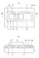
次に、図5(A)、(B)に示すように、第2のオーミックコンタクト層形成用層31a、31bを含むガラス基板1の上面に、プラズマCVD法により、真性酸化亜鉛からなる半導体薄膜形成用膜15aおよび窒化シリコンからなる保護膜形成用膜16aを連続して成膜する。次に、保護膜形成用膜16aの上面の所定の箇所に、フォトリソグラフィ法により、デバイスエリア形成用のレジストパターン33を形成する。 Next, as shown in FIGS. 5A and 5B, a semiconductor thin film made of intrinsic zinc oxide is formed on the upper surface of the
次に、レジストパターン33をマスクとして、保護膜形成用膜16aをエッチングすると、図6(A)、(B)に示すように、レジストパターン33下に保護膜16が形成される。この場合、レジストパターン33下以外の領域における半導体薄膜形成用膜15aの表面が露出される。そこで、窒化シリコンからなる保護膜形成用膜16aのエッチング方法としては、保護膜形成用膜16aのエッチング速度は速いが、真性酸化亜鉛からなる半導体薄膜形成用膜15aをなるべく侵さないようにするために、六フッ化イオウ(SF6)を用いた反応性プラズマエッチング(ドライエッチング)が好ましい。Next, when the protective
次に、レジストパターン33をレジスト剥離液を用いて剥離する。この場合、保護膜16下以外の領域における半導体薄膜形成用膜15aの表面がレジスト剥離液に曝されるが、この曝された部分はデバイスエリア以外であるので、別に支障はない。すなわち、オーミックコンタクト層の場合と異なり、チャネル領域のサイドエッチングおよびチャネル領域の上面のエッチングは薄膜トランジスタの特性に大きな影響を与える。しかしながら、本発明においては、保護膜16下の半導体薄膜形成用膜15aは保護膜16によって保護されている。なお、この場合のレジスト剥離液として、酸性もアルカリ性も呈さない(電解質を含まない)もの、例えば、単一の有機溶媒(例えばジメチルスルホキシド(DMSO))を用いてもよい。 Next, the resist
次に、保護膜16をマスクとして、半導体薄膜形成用膜15aおよび第2のオーミックコンタクト層形成用層31a、31bを連続してエッチングすると、図7(A)、(B)に示すように、保護膜16下に半導体薄膜15が形成され、半導体薄膜15下の両側にオーミックコンタクト層13、14が形成される。 Next, when the semiconductor thin
この場合、半導体薄膜形成用膜15aおよび第2のオーミックコンタクト層形成用層31a、31bは真性酸化亜鉛およびn型酸化亜鉛によって形成されているため、エッチング液として上記水酸化ナトリウム水溶液を用いると、加工の制御性を良好とすることができる。ここで、2つのオーミックコンタクト層13、14間の間隔がチャネル長Lとなり、オーミックコンタクト層13、14のチャネル長Lに直交する方向の寸法がチャネル幅Wとなる。 In this case, since the semiconductor thin
なお、上記では、レジストパターン33を剥離した後、保護膜16をマスクとして、半導体薄膜形成用膜15aおよび第2のオーミックコンタクト層形成用層31a、31bをエッチングする順序としているが、半導体薄膜形成用膜15aおよび第2のオーミックコンタクト層形成用層31a、31bをエッチングした後、レジストパターン33を剥離するようにしてもよい。 In the above description, after the resist
次に、図8(A)、(B)に示すように、保護膜16、ソース電極11およびデータライン3を含むガラス基板1の上面に、プラズマCVD法により、窒化シリコンからなる絶縁膜17を成膜する。次に、絶縁膜17の上面の所定の箇所に、スパッタ法により成膜されたクロム、アルミニウム、ITOなどからなる金属膜をフォトリソグラフィ法によりパターニングすることにより、ゲート電極18および該ゲート電極18に接続された走査ライン2を形成する。 Next, as shown in FIGS. 8A and 8B, an insulating
次に、図9(A)、(B)に示すように、ゲート電極18および走査ライン2を含む絶縁膜17の上面に、プラズマCVD法により、窒化シリコンからなる上層絶縁膜19を成膜する。次に、上層絶縁膜19の上面の所定の箇所に、スパッタ法により成膜されたクロム、アルミニウムなどからなる遮光性金属膜をフォトリソグラフィ法によりパターニングすることにより、補助容量電極6を形成する。 Next, as shown in FIGS. 9A and 9B, an upper insulating
次に、図2(A)、(B)に示すように、補助容量電極6を含む上層絶縁膜19の上面に、プラズマCVD法により、窒化シリコンからなるオーバーコート膜20を成膜する。次に、ソース電極15の所定の箇所に対応する部分におけるオーバーコート膜20、上層絶縁膜19および絶縁膜17に、フォトリソグラフィ法により、コンタクトホール21を連続して形成する。次に、オーバーコート膜20の上面の所定の箇所に、スパッタ法により成膜されたITOなどの透明導電材料からなる画素電極形成用膜をフォトリソグラフィ法によりパターニングすることにより、画素電極4をコンタクトホール21を介してソース電極11に接続させて形成する。かくして、図2(A)、(B)に示す液晶表示装置が得られる。 Next, as shown in FIGS. 2A and 2B, an
以上のように、上記製造方法では、半導体薄膜形成用膜15aの上面に保護膜16を形成するためのレジストパターン33を剥離するとき、保護膜16下の半導体薄膜形成用膜15aを保護膜16で保護し、次いで保護膜16をマスクとして半導体薄膜形成用膜15aおよび第2のオーミックコトタクト層形成用層31a、31bを連続してエッチングすることにより、保護膜16下に半導体薄膜15を形成し、半導体薄膜15下の両側にオーミックコトタクト層13、14を形成し、そして半導体薄膜15の上面全体に保護膜16をそのまま残しているので、加工精度を良くすることができる。 As described above, in the above manufacturing method, when the resist
また、上記製造方法により得られた薄膜トランジスタ5では、2つのオーミックコンタクト層13、14間の間隔がチャネル長Lとなり、オーミックコンタクト層13、14のチャネル長Lに直交する方向の寸法がチャネル幅Wとなるので、その寸法をボトムゲート構造でチャネルエッチ型の薄膜トランジスタの寸法と同等とすることができ、ひいては小型化することができる。 In the
さらに、上記製造方法により得られた液晶表示装置では、画素電極4と走査ライン2およびデータライン3との間に走査ライン2およびデータライン3の幅よりも広い幅を有する第1、第2の補助容量電極部6a、6bを設けているので、この第1、第2の補助容量電極部6a、6bにより、画素電極4と走査ライン2およびデータライン3との間に結合容量が発生するのを防止することができ、したがって垂直クロストークが発生しないようにすることができ、表示特性を向上することができる。 Further, in the liquid crystal display device obtained by the above manufacturing method, the first and second electrodes having a width wider than the width of the
なお、当初の工程において、ガラス基板1の上面にソース・ドレイン電極形成用膜および第1のオーミックコンタクト層形成用層31を連続して成膜し、第1のオーミックコンタクト層形成用層31の上面に例えば図3(A)、(B)に示すようなレジストパターン32a、32bを形成し、レジストパターン32a、32bをマスクとして第1のオーミックコンタクト層形成用層31およびソース・ドレイン電極形成用膜を連続してエッチングすることにより、例えば図4(A)、(B)に示すように、レジストパターン32a、32b下に第2のオーミックコンタクト層形成用層31a、31bを形成し、第2のオーミックコンタクト層形成用層31a、31b下にソース電極11およびドレイン電極12を形成するようにしてもよい。 In the initial step, the source / drain electrode formation film and the first ohmic contact
(第2実施形態)
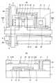
図10(A)はこの発明の第2実施形態としての薄膜トランジスタを備えた液晶表示装置の要部の透過平面図を示し、図10(B)は図10(A)のXB−XB線に沿う断面図を示す。この液晶表示装置において、図2(A)、(B)に示す液晶表示装置と異なる点は、ソース電極11の上面のドレイン電極12側の所定の箇所およびその近傍のガラス基板1の上面に一方のオーミックコンタクト層13を設け、データライン3の一部を含むドレイン電極12の上面のソース電極11側の所定の箇所およびその近傍のガラス基板1の上面に他方のオーミックコンタクト層14を設けた点である。すなわち、ソース電極11およびドレイン電極12の各上面にはそれぞれオーミックコンタクト層13、14がその互いに対向する端面13a、14aをソース電極11およびドレイン電極12の互いに対向する端面11a、12aから突出されて設けられている。(Second Embodiment)
FIG. 10A shows a transmission plan view of the main part of a liquid crystal display device having a thin film transistor as a second embodiment of the present invention, and FIG. 10B shows a line XB -XB in FIG. FIG. In this liquid crystal display device, the difference from the liquid crystal display device shown in FIGS. 2A and 2B is that a predetermined portion on the
次に、この液晶表示装置における薄膜トランジスタ5の部分の製造方法の一例について説明する。まず、図11(A)、(B)に示すように、ガラス基板1の上面の各所定の箇所に、スパッタ法により成膜されたアルミニウム、クロム、ITOなどからなる金属膜をフォトリソグラフィ法によりパターニングすることにより、ソース電極11、ドレイン電極12および該ドレイン電極12に接続されたデータライン3を形成する。 Next, an example of a method for manufacturing the
次に、ソース電極11、ドレイン電極12およびデータライン3を含むガラス基板1の上面に、対向ターゲット方式のスパッリングにより、n型酸化亜鉛からなる第1のオーミックコンタクト層形成用層31を成膜する。次に、第1のオーミックコンタクト層形成用層31の上面の各所定の箇所に、フォトリソグラフィ法により、レジストパターン32a、32bを形成する。 Next, a first ohmic contact
この場合、一方のレジストパターン32aは、ソース電極11よりもある程度大きめで、ソース電極11を完全に覆うように形成する。他方のレジストパターン32bは、データライン3の一部を含むドレイン電極12よりもある程度大きめで、データライン3の一部を含むドレイン電極12を完全に覆うように形成する。 In this case, one resist
レジストパターン32a、32bをこのように形成するのは、図10(A)、(B)を参照して説明すると、例えば、ソース電極11の端面11aと一方のオーミックコンタクト層13の端面13aとの間隔がこれらの端面11a、13aの位置関係を所望の関係に保つためのマージンであり、加工精度にもよるが、一般的に、1〜4μm必要であるからである。 The resist
次に、レジストパターン32a、32bをマスクとして、第1のオーミックコンタクト層形成用層31をエッチングすると、図12(A)、(B)に示すように、レジストパターン21下に第2のオーミックコンタクト層形成用層31a、31bが形成される。この場合、第1のオーミックコンタクト層形成用層31はn型酸化亜鉛によって形成されているため、エッチング液として上記水酸化ナトリウムを用いると、加工の制御性を良好とすることができる。 Next, when the first ohmic contact
次に、レジストパターン32a、32bをレジスト剥離液を用いて剥離する。この場合、第2のオーミックコンタクト層形成用層31a、31bの表面が露出される。したがって、この場合のレジスト剥離液としては、酸性もアルカリ性も呈さない(電解質を含まない)もの、例えば、単一の有機溶媒(例えばジメチルスルホキシド(DMSO))を用いる。 Next, the resist
次に、図13(A)、(B)に示すように、第2のオーミックコンタクト層形成用層31a、31bおよびデータライン3を含むガラス基板1の上面に、プラズマCVD法により、真性酸化亜鉛からなる半導体薄膜形成用膜15aおよび窒化シリコンからなる保護膜形成用膜16aを連続して成膜する。次に、保護膜形成用膜16aの上面の所定の箇所に、フォトリソグラフィ法により、デバイスエリア形成用のレジストパターン33を形成する。 Next, as shown in FIGS. 13A and 13B, intrinsic zinc oxide is formed on the upper surface of the
次に、レジストパターン33をマスクとして、保護膜形成用膜16aをエッチングすると、図14(A)、(B)に示すように、レジストパターン33下に保護膜16が形成される。この場合、レジストパターン33下以外の領域における半導体薄膜形成用膜15aの表面が露出される。したがって、窒化シリコンからなる保護膜16を形成するためのエッチング方法としては、六フッ化イオウ(SF6)を用いた反応性プラズマエッチング(ドライエッチング)が好ましい。Next, when the protective
次に、レジストパターン33をレジスト剥離液を用いて剥離する。この場合、保護膜16下以外の領域における半導体薄膜形成用膜15aの表面がレジスト剥離液に曝されるが、この曝された部分はデバイスエリア以外であるので、別に支障はない。すなわち、保護膜16下の半導体薄膜形成用膜15aは保護膜16によって保護されている。なお、この場合のレジスト剥離液として、酸性もアルカリ性も呈さない(電解質を含まない)もの、例えば、単一の有機溶媒(例えばジメチルスルホキシド(DMSO))を用いてもよい。 Next, the resist
次に、保護膜16をマスクとして、半導体薄膜形成用膜15aおよび第2のオーミックコンタクト層形成用層31a、31bを連続してエッチングすると、図15(A)、(B)に示すように、保護膜16下に半導体薄膜15が形成され、半導体薄膜15下の両側にオーミックコンタクト層13、14が形成される。 Next, when the semiconductor thin
この場合、半導体薄膜形成用膜15aおよび第2のオーミックコンタクト層形成用層31a、31bは真性酸化亜鉛およびn型酸化亜鉛によって形成されているため、エッチング液として上記水酸化ナトリウム水溶液を用いると、加工の制御性を良好とすることができる。ここで、2つのオーミックコンタクト層13、14間の間隔がチャネル長Lとなり、オーミックコンタクト層13、14のチャネル長Lに直交する方向の寸法がチャネル幅Wとなる。以下、上記第1実施形態の場合と同様の工程を経ると、図10(A)、(B)に示す液晶表示装置が得られる。 In this case, since the semiconductor thin
(第3実施形態)
図16(A)はこの発明の第3実施形態としての薄膜トランジスタを備えた液晶表示装置の要部の透過平面図を示し、図16(B)は図16(A)のXVIB−XVIB線に沿う断面図を示す。この液晶表示装置において、図2(A)、(B)に示す液晶表示装置と異なる点は、上層絶縁膜16を設けずに、絶縁膜17の上面の各所定の箇所にアルミニウム、クロムなどの遮光性金属からなるゲート電極18、該ゲート電極18に接続された走査ライン2および補助容量電極6を設けた点である。(Third embodiment)
FIG. 16A shows a transmission plan view of the main part of a liquid crystal display device having a thin film transistor as a third embodiment of the present invention, and FIG. 16B shows the XVIB -XVIB line of FIG. FIG. In this liquid crystal display device, the difference from the liquid crystal display device shown in FIGS. 2A and 2B is that the upper insulating
この場合、補助容量電極6は、データライン3の一部と重ね合わされた部分を含む第1の補助容量電極部6dと、走査ライン2の近傍に走査ライン2と平行に配置された第2の補助容量電極部6eと、画素電極4の所定の縁部に沿って配置された第3の補助容量電極部6fとからなっている。 In this case, the
この液晶表示装置の薄膜トランジスタ5の部分の製造方法では、絶縁膜17の上面の各所定の箇所にアルミニウム、クロムなどの遮光性金属からなるゲート電極18、該ゲート電極18に接続された走査ライン2および補助容量電極6を同時に形成することができるので、図2(A)、(B)に示す場合と比較して、上層絶縁膜を成膜する工程、補助容量電極形成用膜を成膜する工程、補助容量電極形成用のレジストパターンを形成する工程、レジストパターンをマスクとして補助容量電極形成用膜をエッチングして補助容量電極を形成する工程、レジストパターンを剥離する工程を省略することができ、工程数を低減することができる。 In this method of manufacturing the
(その他の実施形態)
半導体薄膜形成用膜15aおよびオーミックコンタクト層形成用層31の成膜は、プラズマCVD法に限らず、スパッタ法、蒸着法、キャスト法、メッキ法などであってもよい。また、オーミックコンタクト層13、14は、n型酸化亜鉛に限らず、p型酸化亜鉛であってもよく、また酸素欠損を生じさせて導電率を変化させた酸化亜鉛であってもよい。(Other embodiments)
The film formation of the semiconductor thin
また、ガラス基板1とソース電極11およびドレイン電極12との間に下地絶縁膜を設けるようにしてもよい。例えば、下地絶縁膜をイオンバリア性材料によって形成した場合には、ガラス基板1からの不純物拡散を抑制することができ、またガラス基板1と酸化亜鉛膜との反応を抑制することができる。下地絶縁膜の材質として、格子定数や結晶構造が酸化亜鉛に近いものを選択した場合には、酸化亜鉛膜の結晶性を向上させることができる。 Further, a base insulating film may be provided between the
1 ガラス基板
2 走査ライン
3 データライン
4 画素電極
5 薄膜トランジスタ
6 補助容量電極
11 ソース電極
12 ドレイン電極
13、14 オーミックコンタクト層
15 半導体薄膜
16 保護膜
17 絶縁膜
18 ゲート電極
19 上層絶縁膜
20 オーバーコート膜
21 コンタクトホールDESCRIPTION OF
Claims (11)
Translated fromJapanesePriority Applications (9)
| Application Number | Priority Date | Filing Date | Title |
|---|---|---|---|
| JP2005170348AJP2006344849A (en) | 2005-06-10 | 2005-06-10 | Thin film transistor |
| US11/448,633US7566904B2 (en) | 2005-06-10 | 2006-06-07 | Thin film transistor having oxide semiconductor layer and manufacturing method thereof |
| EP06757369.1AEP1889298B1 (en) | 2005-06-10 | 2006-06-09 | Manufacturing method for hin film transistor having channel comprising zinc oxide |
| PCT/JP2006/312076WO2006132439A1 (en) | 2005-06-10 | 2006-06-09 | Thin film transistor having channel comprising zinc oxide and manufacturing method thereof |
| EP19219861.2AEP3651209B1 (en) | 2005-06-10 | 2006-06-09 | Liquid crystal display comprising thin film transistor having channel comprising zinc oxide |
| KR1020077019261AKR100908557B1 (en) | 2005-06-10 | 2006-06-09 | Thin film transistor having a channel containing zinc oxide and method of manufacturing the same |
| TW095120491ATWI302034B (en) | 2005-06-10 | 2006-06-09 | Thin film transistor and manufacturing method thereof |
| CN200680006306ACN100583457C (en) | 2005-06-10 | 2006-06-09 | Thin film transistor having channel comprising zinc oxide and manufacturing method thereof |
| US12/190,102US7585698B2 (en) | 2005-06-10 | 2008-08-12 | Thin film transistor having oxide semiconductor layer and manufacturing method thereof |
Applications Claiming Priority (1)
| Application Number | Priority Date | Filing Date | Title |
|---|---|---|---|
| JP2005170348AJP2006344849A (en) | 2005-06-10 | 2005-06-10 | Thin film transistor |
Related Child Applications (1)
| Application Number | Title | Priority Date | Filing Date |
|---|---|---|---|
| JP2006046072ADivisionJP4458048B2 (en) | 2006-02-23 | 2006-02-23 | Thin film transistor manufacturing method |
Publications (1)
| Publication Number | Publication Date |
|---|---|
| JP2006344849Atrue JP2006344849A (en) | 2006-12-21 |
Family
ID=36822355
Family Applications (1)
| Application Number | Title | Priority Date | Filing Date |
|---|---|---|---|
| JP2005170348APendingJP2006344849A (en) | 2005-06-10 | 2005-06-10 | Thin film transistor |
Country Status (7)
| Country | Link |
|---|---|
| US (2) | US7566904B2 (en) |
| EP (2) | EP1889298B1 (en) |
| JP (1) | JP2006344849A (en) |
| KR (1) | KR100908557B1 (en) |
| CN (1) | CN100583457C (en) |
| TW (1) | TWI302034B (en) |
| WO (1) | WO2006132439A1 (en) |
Cited By (9)
| Publication number | Priority date | Publication date | Assignee | Title |
|---|---|---|---|---|
| JP2007073561A (en)* | 2005-09-02 | 2007-03-22 | Kochi Prefecture Sangyo Shinko Center | Thin film transistor |
| JP2007165861A (en)* | 2005-11-15 | 2007-06-28 | Semiconductor Energy Lab Co Ltd | Semiconductor device and manufacturing method thereof |
| JP2008060099A (en)* | 2006-08-29 | 2008-03-13 | Casio Comput Co Ltd | Thin film transistor and manufacturing method thereof |
| JP2009152633A (en)* | 2005-11-15 | 2009-07-09 | Semiconductor Energy Lab Co Ltd | Method for manufacturing semiconductor device and method for manufacturing liquid crystal display device |
| JP2014239244A (en)* | 2008-12-25 | 2014-12-18 | 株式会社半導体エネルギー研究所 | Semiconductor device |
| JP2015144290A (en)* | 2009-03-27 | 2015-08-06 | 株式会社半導体エネルギー研究所 | Display device |
| JP2015207781A (en)* | 2008-08-08 | 2015-11-19 | 株式会社半導体エネルギー研究所 | semiconductor device |
| JP2017017344A (en)* | 2010-01-22 | 2017-01-19 | 株式会社半導体エネルギー研究所 | Semiconductor device |
| JP2020074461A (en)* | 2010-02-05 | 2020-05-14 | 株式会社半導体エネルギー研究所 | Semiconductor device |
Families Citing this family (1799)
| Publication number | Priority date | Publication date | Assignee | Title |
|---|---|---|---|---|
| US7262463B2 (en)* | 2003-07-25 | 2007-08-28 | Hewlett-Packard Development Company, L.P. | Transistor including a deposited channel region having a doped portion |
| TWI445178B (en) | 2005-01-28 | 2014-07-11 | Semiconductor Energy Lab | Semiconductor device, electronic device, and method of manufacturing semiconductor device |
| TWI505473B (en) | 2005-01-28 | 2015-10-21 | Semiconductor Energy Lab | Semiconductor device, electronic device, and method of manufacturing semiconductor device |
| US7858451B2 (en)* | 2005-02-03 | 2010-12-28 | Semiconductor Energy Laboratory Co., Ltd. | Electronic device, semiconductor device and manufacturing method thereof |
| US7948171B2 (en) | 2005-02-18 | 2011-05-24 | Semiconductor Energy Laboratory Co., Ltd. | Light emitting device |
| US7928938B2 (en)* | 2005-04-19 | 2011-04-19 | Semiconductor Energy Laboratory Co., Ltd. | Semiconductor device including memory circuit, display device and electronic apparatus |
| US8629819B2 (en) | 2005-07-14 | 2014-01-14 | Semiconductor Energy Laboratory Co., Ltd. | Semiconductor device and driving method thereof |
| EP1770788A3 (en) | 2005-09-29 | 2011-09-21 | Semiconductor Energy Laboratory Co., Ltd. | Semiconductor device having oxide semiconductor layer and manufacturing method thereof |
| CN101278403B (en) | 2005-10-14 | 2010-12-01 | 株式会社半导体能源研究所 | Semiconductor device and manufacturing method thereof |
| EP1843194A1 (en) | 2006-04-06 | 2007-10-10 | Semiconductor Energy Laboratory Co., Ltd. | Liquid crystal display device, semiconductor device, and electronic appliance |
| KR100785038B1 (en)* | 2006-04-17 | 2007-12-12 | 삼성전자주식회사 | Amorphous ZnO based Thin Film Transistor |
| JP5116277B2 (en) | 2006-09-29 | 2013-01-09 | 株式会社半導体エネルギー研究所 | Semiconductor device, display device, liquid crystal display device, display module, and electronic apparatus |
| US7646015B2 (en) | 2006-10-31 | 2010-01-12 | Semiconductor Energy Laboratory Co., Ltd. | Manufacturing method of semiconductor device and semiconductor device |
| KR101509663B1 (en) | 2007-02-16 | 2015-04-06 | 삼성전자주식회사 | Method of forming oxide semiconductor layer and method of manufacturing semiconductor device using the same |
| KR101410926B1 (en)* | 2007-02-16 | 2014-06-24 | 삼성전자주식회사 | Thin film transistor and manufacturing method thereof |
| KR101325053B1 (en)* | 2007-04-18 | 2013-11-05 | 삼성디스플레이 주식회사 | Thin film transistor substrate and manufacturing method thereof |
| KR101334181B1 (en)* | 2007-04-20 | 2013-11-28 | 삼성전자주식회사 | Thin Film Transistor having selectively crystallized channel layer and method of manufacturing the same |
| JP5542297B2 (en) | 2007-05-17 | 2014-07-09 | 株式会社半導体エネルギー研究所 | Liquid crystal display device, display module, and electronic device |
| JP4989309B2 (en) | 2007-05-18 | 2012-08-01 | 株式会社半導体エネルギー研究所 | Liquid crystal display |
| EP2153468B1 (en)* | 2007-05-31 | 2010-12-01 | Canon Kabushiki Kaisha | Manufacturing method of thin film transistor using oxide semiconductor |
| JP2010530634A (en) | 2007-06-19 | 2010-09-09 | サムスン エレクトロニクス カンパニー リミテッド | Oxide semiconductor and thin film transistor including the same |
| US7935964B2 (en)* | 2007-06-19 | 2011-05-03 | Samsung Electronics Co., Ltd. | Oxide semiconductors and thin film transistors comprising the same |
| US8354674B2 (en) | 2007-06-29 | 2013-01-15 | Semiconductor Energy Laboratory Co., Ltd. | Semiconductor device wherein a property of a first semiconductor layer is different from a property of a second semiconductor layer |
| WO2009014155A1 (en) | 2007-07-25 | 2009-01-29 | Semiconductor Energy Laboratory Co., Ltd. | Photoelectric conversion device and electronic device having the same |
| KR20090075554A (en) | 2008-01-04 | 2009-07-08 | 삼성전자주식회사 | Liquid Crystal Display and Manufacturing Method Thereof |
| KR101513601B1 (en)* | 2008-03-07 | 2015-04-21 | 삼성전자주식회사 | transistor |
| KR20090108431A (en)* | 2008-04-11 | 2009-10-15 | 삼성전자주식회사 | Display substrate and manufacturing method thereof |
| KR101496148B1 (en)* | 2008-05-15 | 2015-02-27 | 삼성전자주식회사 | Semiconductor device and manufacturing method thereof |
| US9041202B2 (en) | 2008-05-16 | 2015-05-26 | Semiconductor Energy Laboratory Co., Ltd. | Semiconductor device and manufacturing method of the same |
| KR101468591B1 (en)* | 2008-05-29 | 2014-12-04 | 삼성전자주식회사 | Oxide semiconductor and thin film transistor comprising the same |
| US8314765B2 (en) | 2008-06-17 | 2012-11-20 | Semiconductor Energy Laboratory Co., Ltd. | Driver circuit, display device, and electronic device |
| KR101910451B1 (en) | 2008-07-10 | 2018-10-22 | 가부시키가이샤 한도오따이 에네루기 켄큐쇼 | Light-emitting device and electronic device using the same |
| TWI469354B (en) | 2008-07-31 | 2015-01-11 | Semiconductor Energy Lab | Semiconductor device and method of manufacturing same |
| JP2010056541A (en) | 2008-07-31 | 2010-03-11 | Semiconductor Energy Lab Co Ltd | Semiconductor device and manufacturing method thereof |
| JP5616038B2 (en) | 2008-07-31 | 2014-10-29 | 株式会社半導体エネルギー研究所 | Method for manufacturing semiconductor device |
| TWI491048B (en) | 2008-07-31 | 2015-07-01 | Semiconductor Energy Lab | Semiconductor device |
| TWI627757B (en) | 2008-07-31 | 2018-06-21 | 半導體能源研究所股份有限公司 | Semiconductor device |
| JP5608347B2 (en) | 2008-08-08 | 2014-10-15 | 株式会社半導体エネルギー研究所 | Semiconductor device and manufacturing method of semiconductor device |
| TWI508282B (en) | 2008-08-08 | 2015-11-11 | Semiconductor Energy Lab | Semiconductor device and method of manufacturing same |
| JP5525778B2 (en) | 2008-08-08 | 2014-06-18 | 株式会社半導体エネルギー研究所 | Semiconductor device |
| TWI424506B (en) | 2008-08-08 | 2014-01-21 | Semiconductor Energy Lab | Semiconductor device manufacturing method |
| US9082857B2 (en) | 2008-09-01 | 2015-07-14 | Semiconductor Energy Laboratory Co., Ltd. | Semiconductor device comprising an oxide semiconductor layer |
| JP5627071B2 (en) | 2008-09-01 | 2014-11-19 | 株式会社半導体エネルギー研究所 | Method for manufacturing semiconductor device |
| TWI511299B (en) | 2008-09-01 | 2015-12-01 | Semiconductor Energy Lab | Semiconductor device manufacturing method |
| WO2010029865A1 (en) | 2008-09-12 | 2010-03-18 | Semiconductor Energy Laboratory Co., Ltd. | Display device |
| KR101623224B1 (en) | 2008-09-12 | 2016-05-20 | 가부시키가이샤 한도오따이 에네루기 켄큐쇼 | Semiconductor device and method for manufacturing the same |
| KR101657957B1 (en) | 2008-09-12 | 2016-09-20 | 가부시키가이샤 한도오따이 에네루기 켄큐쇼 | Display device |
| KR101767864B1 (en) | 2008-09-12 | 2017-08-11 | 가부시키가이샤 한도오따이 에네루기 켄큐쇼 | Semiconductor device and manufacturing method thereof |
| CN102160105B (en) | 2008-09-19 | 2014-06-11 | 株式会社半导体能源研究所 | Display device and manufacturing method thereof |
| KR101670695B1 (en) | 2008-09-19 | 2016-10-31 | 가부시키가이샤 한도오따이 에네루기 켄큐쇼 | Semiconductor device |
| CN102160184B (en)* | 2008-09-19 | 2014-07-09 | 株式会社半导体能源研究所 | Display device |
| CN102160103B (en) | 2008-09-19 | 2013-09-11 | 株式会社半导体能源研究所 | Display device |
| KR101803264B1 (en) | 2008-09-19 | 2017-12-28 | 가부시키가이샤 한도오따이 에네루기 켄큐쇼 | Semiconductor device |
| KR101611643B1 (en) | 2008-10-01 | 2016-04-11 | 가부시키가이샤 한도오따이 에네루기 켄큐쇼 | Semiconductor device |
| KR101435501B1 (en) | 2008-10-03 | 2014-08-29 | 가부시키가이샤 한도오따이 에네루기 켄큐쇼 | Display device |
| CN101714546B (en) | 2008-10-03 | 2014-05-14 | 株式会社半导体能源研究所 | Display device and manufacturing method thereof |
| EP2172977A1 (en) | 2008-10-03 | 2010-04-07 | Semiconductor Energy Laboratory Co., Ltd. | Display device |
| KR101652693B1 (en) | 2008-10-03 | 2016-09-01 | 가부시키가이샤 한도오따이 에네루기 켄큐쇼 | Display device |
| EP2172804B1 (en) | 2008-10-03 | 2016-05-11 | Semiconductor Energy Laboratory Co, Ltd. | Display device |
| CN101719493B (en) | 2008-10-08 | 2014-05-14 | 株式会社半导体能源研究所 | Display device |
| JP5484853B2 (en) | 2008-10-10 | 2014-05-07 | 株式会社半導体エネルギー研究所 | Method for manufacturing semiconductor device |
| KR101799601B1 (en) | 2008-10-16 | 2017-11-20 | 가부시키가이샤 한도오따이 에네루기 켄큐쇼 | Light-emitting display device |
| JP5361651B2 (en) | 2008-10-22 | 2013-12-04 | 株式会社半導体エネルギー研究所 | Method for manufacturing semiconductor device |
| EP2180518B1 (en) | 2008-10-24 | 2018-04-25 | Semiconductor Energy Laboratory Co, Ltd. | Method for manufacturing semiconductor device |
| WO2010047288A1 (en) | 2008-10-24 | 2010-04-29 | Semiconductor Energy Laboratory Co., Ltd. | Method for manufacturing semiconductordevice |
| JP5616012B2 (en) | 2008-10-24 | 2014-10-29 | 株式会社半導体エネルギー研究所 | Method for manufacturing semiconductor device |
| JP5442234B2 (en) | 2008-10-24 | 2014-03-12 | 株式会社半導体エネルギー研究所 | Semiconductor device and display device |
| KR101667909B1 (en) | 2008-10-24 | 2016-10-28 | 가부시키가이샤 한도오따이 에네루기 켄큐쇼 | Method for manufacturing semiconductor device |
| US8741702B2 (en) | 2008-10-24 | 2014-06-03 | Semiconductor Energy Laboratory Co., Ltd. | Method for manufacturing semiconductor device |
| KR20160072845A (en) | 2008-10-24 | 2016-06-23 | 가부시키가이샤 한도오따이 에네루기 켄큐쇼 | Semiconductor device and method for manufacturing the same |
| US8106400B2 (en) | 2008-10-24 | 2012-01-31 | Semiconductor Energy Laboratory Co., Ltd. | Semiconductor device and method for manufacturing the same |
| KR101547325B1 (en)* | 2008-10-27 | 2015-08-26 | 삼성전자주식회사 | Transistor and semiconductor device comprising the same |
| KR101631454B1 (en) | 2008-10-31 | 2016-06-17 | 가부시키가이샤 한도오따이 에네루기 켄큐쇼 | Logic circuit |
| WO2010050419A1 (en) | 2008-10-31 | 2010-05-06 | Semiconductor Energy Laboratory Co., Ltd. | Driver circuit and display device |
| KR101603303B1 (en) | 2008-10-31 | 2016-03-14 | 가부시키가이샤 한도오따이 에네루기 켄큐쇼 | Conductive oxynitride and method for manufacturing conductive oxynitride film |
| TWI567829B (en) | 2008-10-31 | 2017-01-21 | 半導體能源研究所股份有限公司 | Semiconductor device and method of manufacturing same |
| EP2184783B1 (en) | 2008-11-07 | 2012-10-03 | Semiconductor Energy Laboratory Co, Ltd. | Semiconductor device and method for manufacturing the same |
| TWI606595B (en) | 2008-11-07 | 2017-11-21 | 半導體能源研究所股份有限公司 | Semiconductor device and method of manufacturing same |
| TWI487104B (en) | 2008-11-07 | 2015-06-01 | Semiconductor Energy Lab | Semiconductor device and method of manufacturing same |
| CN101740631B (en) | 2008-11-07 | 2014-07-16 | 株式会社半导体能源研究所 | Semiconductor device and method for manufacturing the semiconductor device |
| TWI467663B (en)* | 2008-11-07 | 2015-01-01 | Semiconductor Energy Lab | Semiconductor device and method of manufacturing the same |
| KR20170021903A (en)* | 2008-11-07 | 2017-02-28 | 가부시키가이샤 한도오따이 에네루기 켄큐쇼 | Method of manufacturing a semiconductor device |
| TWI656645B (en) | 2008-11-13 | 2019-04-11 | 日商半導體能源研究所股份有限公司 | Semiconductor device and method of manufacturing same |
| KR101432764B1 (en) | 2008-11-13 | 2014-08-21 | 가부시키가이샤 한도오따이 에네루기 켄큐쇼 | Method for manufacturing semiconductor device |
| US8232947B2 (en) | 2008-11-14 | 2012-07-31 | Semiconductor Energy Laboratory Co., Ltd. | Liquid crystal display device |
| JP2010153802A (en) | 2008-11-20 | 2010-07-08 | Semiconductor Energy Lab Co Ltd | Semiconductor device and method of manufacturing the same |
| KR101914404B1 (en) | 2008-11-21 | 2018-11-01 | 가부시키가이샤 한도오따이 에네루기 켄큐쇼 | Semiconductor device |
| TWI749283B (en) | 2008-11-28 | 2021-12-11 | 日商半導體能源研究所股份有限公司 | Liquid crystal display device |
| TWI585955B (en) | 2008-11-28 | 2017-06-01 | 半導體能源研究所股份有限公司 | Light sensor and display device |
| TWI506795B (en) | 2008-11-28 | 2015-11-01 | Semiconductor Energy Lab | Semiconductor device and method of manufacturing same |
| KR101643204B1 (en) | 2008-12-01 | 2016-07-27 | 가부시키가이샤 한도오따이 에네루기 켄큐쇼 | Semiconductor device and manufacturing method thereof |
| TWI633371B (en) | 2008-12-03 | 2018-08-21 | 半導體能源研究所股份有限公司 | Liquid crystal display device |
| JP5491833B2 (en) | 2008-12-05 | 2014-05-14 | 株式会社半導体エネルギー研究所 | Semiconductor device |
| WO2010071183A1 (en) | 2008-12-19 | 2010-06-24 | Semiconductor Energy Laboratory Co., Ltd. | Method for manufacturing semiconductor device |
| CN103456794B (en) | 2008-12-19 | 2016-08-10 | 株式会社半导体能源研究所 | How Transistors Are Made |
| EP2515337B1 (en) | 2008-12-24 | 2016-02-24 | Semiconductor Energy Laboratory Co., Ltd. | Driver circuit and semiconductor device |
| US8114720B2 (en) | 2008-12-25 | 2012-02-14 | Semiconductor Energy Laboratory Co., Ltd. | Semiconductor device and manufacturing method thereof |
| US8441007B2 (en) | 2008-12-25 | 2013-05-14 | Semiconductor Energy Laboratory Co., Ltd. | Display device and manufacturing method thereof |
| US20100165280A1 (en)* | 2008-12-25 | 2010-07-01 | Semiconductor Energy Laboratory Co., Ltd. | Liquid crystal display device |
| TWI501319B (en)* | 2008-12-26 | 2015-09-21 | Semiconductor Energy Lab | Semiconductor device and manufacturing method thereof |
| JP5590877B2 (en)* | 2008-12-26 | 2014-09-17 | 株式会社半導体エネルギー研究所 | Semiconductor device |
| KR101648927B1 (en) | 2009-01-16 | 2016-08-17 | 가부시키가이샤 한도오따이 에네루기 켄큐쇼 | Semiconductor device and manufacturing method thereof |
| US8492756B2 (en) | 2009-01-23 | 2013-07-23 | Semiconductor Energy Laboratory Co., Ltd. | Semiconductor device and method for manufacturing the same |
| US8436350B2 (en)* | 2009-01-30 | 2013-05-07 | Semiconductor Energy Laboratory Co., Ltd. | Semiconductor device using an oxide semiconductor with a plurality of metal clusters |
| US8367486B2 (en) | 2009-02-05 | 2013-02-05 | Semiconductor Energy Laboratory Co., Ltd. | Transistor and method for manufacturing the transistor |
| US8174021B2 (en) | 2009-02-06 | 2012-05-08 | Semiconductor Energy Laboratory Co., Ltd. | Semiconductor device and method of manufacturing the semiconductor device |
| US8749930B2 (en) | 2009-02-09 | 2014-06-10 | Semiconductor Energy Laboratory Co., Ltd. | Protection circuit, semiconductor device, photoelectric conversion device, and electronic device |
| US8278657B2 (en) | 2009-02-13 | 2012-10-02 | Semiconductor Energy Laboratory Co., Ltd. | Transistor, semiconductor device including the transistor, and manufacturing method of the transistor and the semiconductor device |
| US8247812B2 (en) | 2009-02-13 | 2012-08-21 | Semiconductor Energy Laboratory Co., Ltd. | Transistor, semiconductor device including the transistor, and manufacturing method of the transistor and the semiconductor device |
| CN101840936B (en) | 2009-02-13 | 2014-10-08 | 株式会社半导体能源研究所 | Semiconductor device including a transistor, and manufacturing method of the semiconductor device |
| US8247276B2 (en) | 2009-02-20 | 2012-08-21 | Semiconductor Energy Laboratory Co., Ltd. | Thin film transistor, method for manufacturing the same, and semiconductor device |
| US8841661B2 (en) | 2009-02-25 | 2014-09-23 | Semiconductor Energy Laboratory Co., Ltd. | Staggered oxide semiconductor TFT semiconductor device and manufacturing method thereof |
| US8704216B2 (en) | 2009-02-27 | 2014-04-22 | Semiconductor Energy Laboratory Co., Ltd. | Semiconductor device and manufacturing method thereof |
| US20100224878A1 (en) | 2009-03-05 | 2010-09-09 | Semiconductor Energy Laboratory Co., Ltd. | Semiconductor device |
| US8461582B2 (en) | 2009-03-05 | 2013-06-11 | Semiconductor Energy Laboratory Co., Ltd. | Semiconductor device and method for manufacturing the same |
| JP5504008B2 (en) | 2009-03-06 | 2014-05-28 | 株式会社半導体エネルギー研究所 | Semiconductor device |
| KR102391280B1 (en) | 2009-03-12 | 2022-04-28 | 가부시키가이샤 한도오따이 에네루기 켄큐쇼 | Semiconductor device |
| TWI485781B (en) | 2009-03-13 | 2015-05-21 | Semiconductor Energy Lab | Semiconductor device and method of manufacturing the same |
| US8450144B2 (en) | 2009-03-26 | 2013-05-28 | Semiconductor Energy Laboratory Co., Ltd. | Semiconductor device and method for manufacturing the same |
| KR101752640B1 (en) | 2009-03-27 | 2017-06-30 | 가부시키가이샤 한도오따이 에네루기 켄큐쇼 | Semiconductor device |
| KR101681884B1 (en) | 2009-03-27 | 2016-12-05 | 가부시키가이샤 한도오따이 에네루기 켄큐쇼 | Semiconductor device, display device, and electronic appliance |
| US8927981B2 (en) | 2009-03-30 | 2015-01-06 | Semiconductor Energy Laboratory Co., Ltd. | Semiconductor device and method for manufacturing the same |
| US8338226B2 (en) | 2009-04-02 | 2012-12-25 | Semiconductor Energy Laboratory Co., Ltd. | Method for manufacturing semiconductor device |
| TWI489628B (en) | 2009-04-02 | 2015-06-21 | Semiconductor Energy Lab | Semiconductor device and method of manufacturing same |
| JP5615018B2 (en) | 2009-04-10 | 2014-10-29 | 株式会社半導体エネルギー研究所 | Semiconductor device and manufacturing method of semiconductor device |
| TWI535023B (en) | 2009-04-16 | 2016-05-21 | 半導體能源研究所股份有限公司 | Semiconductor device and method of manufacturing same |
| JP5669426B2 (en)* | 2009-05-01 | 2015-02-12 | 株式会社半導体エネルギー研究所 | Method for manufacturing semiconductor device |
| JP5751762B2 (en) | 2009-05-21 | 2015-07-22 | 株式会社半導体エネルギー研究所 | Semiconductor device |
| EP2256814B1 (en) | 2009-05-29 | 2019-01-16 | Semiconductor Energy Laboratory Co, Ltd. | Oxide semiconductor device and method for manufacturing the same |
| JP5564331B2 (en) | 2009-05-29 | 2014-07-30 | 株式会社半導体エネルギー研究所 | Method for manufacturing semiconductor device |
| EP2256795B1 (en) | 2009-05-29 | 2014-11-19 | Semiconductor Energy Laboratory Co., Ltd. | Manufacturing method for oxide semiconductor device |
| KR101732859B1 (en) | 2009-06-30 | 2017-05-04 | 가부시키가이샤 한도오따이 에네루기 켄큐쇼 | Method for manufacturing semiconductor device |
| KR102011616B1 (en) | 2009-06-30 | 2019-08-16 | 가부시키가이샤 한도오따이 에네루기 켄큐쇼 | Method for manufacturing semiconductor device |
| KR101810699B1 (en) | 2009-06-30 | 2018-01-25 | 가부시키가이샤 한도오따이 에네루기 켄큐쇼 | Method for manufacturing semiconductor device |
| WO2011001881A1 (en) | 2009-06-30 | 2011-01-06 | Semiconductor Energy Laboratory Co., Ltd. | Method for manufacturing semiconductor device |
| KR102503687B1 (en) | 2009-07-03 | 2023-02-27 | 가부시키가이샤 한도오따이 에네루기 켄큐쇼 | Method for manufacturing semiconductor device |
| KR101476817B1 (en) | 2009-07-03 | 2014-12-26 | 가부시키가이샤 한도오따이 에네루기 켄큐쇼 | Display device including transistor and manufacturing method thereof |
| JP5663214B2 (en)* | 2009-07-03 | 2015-02-04 | 株式会社半導体エネルギー研究所 | Method for manufacturing semiconductor device |
| KR101791370B1 (en) | 2009-07-10 | 2017-10-27 | 가부시키가이샤 한도오따이 에네루기 켄큐쇼 | Semiconductor device |
| KR102798889B1 (en) | 2009-07-10 | 2025-04-23 | 가부시키가이샤 한도오따이 에네루기 켄큐쇼 | Method for manufacturing liquid crystal display device |
| KR101857405B1 (en) | 2009-07-10 | 2018-05-11 | 가부시키가이샤 한도오따이 에네루기 켄큐쇼 | Semiconductor device and method for manufacturing the same |
| WO2011007677A1 (en) | 2009-07-17 | 2011-01-20 | Semiconductor Energy Laboratory Co., Ltd. | Semiconductor device and method for manufacturing the same |
| WO2011007682A1 (en) | 2009-07-17 | 2011-01-20 | Semiconductor Energy Laboratory Co., Ltd. | Method of manufacturing semiconductor device |
| KR101739154B1 (en) | 2009-07-17 | 2017-05-23 | 가부시키가이샤 한도오따이 에네루기 켄큐쇼 | Semiconductor device and manufacturing method thereof |
| CN102751295B (en) | 2009-07-18 | 2015-07-15 | 株式会社半导体能源研究所 | Semiconductor device and method for manufacturing semiconductor device |
| CN105070749B (en) | 2009-07-18 | 2019-08-09 | 株式会社半导体能源研究所 | Semiconductor device and method of manufacturing semiconductor device |
| WO2011010541A1 (en) | 2009-07-18 | 2011-01-27 | Semiconductor Energy Laboratory Co., Ltd. | Semiconductor device and method for manufacturing the same |
| WO2011010545A1 (en) | 2009-07-18 | 2011-01-27 | Semiconductor Energy Laboratory Co., Ltd. | Semiconductor device and method for manufacturing the same |
| WO2011010542A1 (en) | 2009-07-23 | 2011-01-27 | Semiconductor Energy Laboratory Co., Ltd. | Semiconductor device and method for manufacturing the same |
| KR101904811B1 (en) | 2009-07-24 | 2018-10-05 | 가부시키가이샤 한도오따이 에네루기 켄큐쇼 | Semiconductor device |
| KR101799252B1 (en) | 2009-07-31 | 2017-11-17 | 가부시키가이샤 한도오따이 에네루기 켄큐쇼 | Semiconductor device and method for manufacturing the same |
| WO2011013596A1 (en) | 2009-07-31 | 2011-02-03 | Semiconductor Energy Laboratory Co., Ltd. | Semiconductor device and manufacturing method thereof |
| KR102097932B1 (en) | 2009-07-31 | 2020-04-06 | 가부시키가이샤 한도오따이 에네루기 켄큐쇼 | Semiconductor device and manufacturing method thereof |
| WO2011013523A1 (en) | 2009-07-31 | 2011-02-03 | Semiconductor Energy Laboratory Co., Ltd. | Semiconductor device and method for manufacturing the same |
| WO2011013502A1 (en)* | 2009-07-31 | 2011-02-03 | Semiconductor Energy Laboratory Co., Ltd. | Semiconductor device and manufacturing method thereof |
| JP5642447B2 (en) | 2009-08-07 | 2014-12-17 | 株式会社半導体エネルギー研究所 | Semiconductor device |
| JP5663231B2 (en) | 2009-08-07 | 2015-02-04 | 株式会社半導体エネルギー研究所 | Light emitting device |
| EP2284891B1 (en) | 2009-08-07 | 2019-07-24 | Semiconductor Energy Laboratory Co, Ltd. | Semiconductor device and manufacturing method thereof |
| TWI604594B (en) | 2009-08-07 | 2017-11-01 | 半導體能源研究所股份有限公司 | Semiconductor device and telephone, watch, and display device including the same |
| TWI700810B (en) | 2009-08-07 | 2020-08-01 | 日商半導體能源研究所股份有限公司 | Semiconductor device and method for manufacturing the same |
| TWI596741B (en) | 2009-08-07 | 2017-08-21 | 半導體能源研究所股份有限公司 | Semiconductor device and method of manufacturing same |
| TWI634642B (en) | 2009-08-07 | 2018-09-01 | 半導體能源研究所股份有限公司 | Semiconductor device and method of manufacturing same |
| US8115883B2 (en) | 2009-08-27 | 2012-02-14 | Semiconductor Energy Laboratory Co., Ltd. | Display device and method for manufacturing the same |
| WO2011027649A1 (en)* | 2009-09-02 | 2011-03-10 | Semiconductor Energy Laboratory Co., Ltd. | Semiconductor device including a transistor, and manufacturing method of semiconductor device |
| WO2011027701A1 (en) | 2009-09-04 | 2011-03-10 | Semiconductor Energy Laboratory Co., Ltd. | Light-emitting device and method for manufacturing the same |
| CN104681447A (en) | 2009-09-04 | 2015-06-03 | 株式会社半导体能源研究所 | Manufacturing Method Of Semiconductor Device |
| US9805641B2 (en)* | 2009-09-04 | 2017-10-31 | Semiconductor Energy Laboratory Co., Ltd. | Display device and electronic device including the same |
| CN102598283B (en) | 2009-09-04 | 2016-05-18 | 株式会社半导体能源研究所 | Semiconductor device and manufacturing method thereof |
| WO2011027676A1 (en) | 2009-09-04 | 2011-03-10 | Semiconductor Energy Laboratory Co., Ltd. | Semiconductor device and manufacturing method thereof |
| CN102498570B (en) | 2009-09-04 | 2016-02-10 | 株式会社半导体能源研究所 | Light emitting device and manufacturing method thereof |
| WO2011027702A1 (en) | 2009-09-04 | 2011-03-10 | Semiconductor Energy Laboratory Co., Ltd. | Light-emitting device and method for manufacturing the same |
| WO2011027664A1 (en) | 2009-09-04 | 2011-03-10 | Semiconductor Energy Laboratory Co., Ltd. | Liquid crystal display device and method for manufacturing the same |
| WO2011027656A1 (en) | 2009-09-04 | 2011-03-10 | Semiconductor Energy Laboratory Co., Ltd. | Transistor and display device |
| KR101746198B1 (en) | 2009-09-04 | 2017-06-12 | 가부시키가이샤 한도오따이 에네루기 켄큐쇼 | Display device and electronic device |
| KR20230165355A (en) | 2009-09-16 | 2023-12-05 | 가부시키가이샤 한도오따이 에네루기 켄큐쇼 | Display device |
| US9715845B2 (en) | 2009-09-16 | 2017-07-25 | Semiconductor Energy Laboratory Co., Ltd. | Semiconductor display device |
| WO2011033909A1 (en)* | 2009-09-16 | 2011-03-24 | Semiconductor Energy Laboratory Co., Ltd. | Driver circuit, display device including the driver circuit, and electronic device including the display device |
| KR20190045396A (en) | 2009-09-16 | 2019-05-02 | 가부시키가이샤 한도오따이 에네루기 켄큐쇼 | Transistor |
| WO2011034012A1 (en) | 2009-09-16 | 2011-03-24 | Semiconductor Energy Laboratory Co., Ltd. | Logic circuit, light emitting device, semiconductor device, and electronic device |
| KR101709749B1 (en) | 2009-09-16 | 2017-03-08 | 가부시키가이샤 한도오따이 에네루기 켄큐쇼 | Driving method of display device and display device |
| KR20120068772A (en) | 2009-09-16 | 2012-06-27 | 가부시키가이샤 한도오따이 에네루기 켄큐쇼 | Light-emitting device and manufacturing method thereof |
| KR20220127372A (en) | 2009-09-24 | 2022-09-19 | 가부시키가이샤 한도오따이 에네루기 켄큐쇼 | Oxide semiconductor film and semiconductor device |
| WO2011037010A1 (en) | 2009-09-24 | 2011-03-31 | Semiconductor Energy Laboratory Co., Ltd. | Semiconductor element and method for manufacturing the same |
| WO2011037050A1 (en) | 2009-09-24 | 2011-03-31 | Semiconductor Energy Laboratory Co., Ltd. | Semiconductor device and manufacturing method thereof |
| KR102219095B1 (en) | 2009-09-24 | 2021-02-23 | 가부시키가이샤 한도오따이 에네루기 켄큐쇼 | Semiconductor device and method for manufacturing the same |
| KR101740943B1 (en) | 2009-09-24 | 2017-06-15 | 가부시키가이샤 한도오따이 에네루기 켄큐쇼 | Display device |
| WO2011037008A1 (en)* | 2009-09-24 | 2011-03-31 | Semiconductor Energy Laboratory Co., Ltd. | Method for manufacturing oxide semiconductor film and method for manufacturing semiconductor device |
| TWI512997B (en) | 2009-09-24 | 2015-12-11 | Semiconductor Energy Lab | Semiconductor device, power supply circuit, and method of manufacturing semiconductor device |
| KR101707260B1 (en) | 2009-09-24 | 2017-02-15 | 가부시키가이샤 한도오따이 에네루기 켄큐쇼 | Semiconductor device |
| CN105513644B (en) | 2009-09-24 | 2019-10-15 | 株式会社半导体能源研究所 | Driver circuit, display device including driver circuit, and electronic appliance including display device |
| WO2011040349A1 (en)* | 2009-09-30 | 2011-04-07 | Semiconductor Energy Laboratory Co., Ltd. | Redox capacitor and manufacturing method thereof |
| KR101767035B1 (en)* | 2009-10-01 | 2017-08-10 | 가부시키가이샤 한도오따이 에네루기 켄큐쇼 | Semiconductor device and method for manufacturing the same |
| KR20120084751A (en) | 2009-10-05 | 2012-07-30 | 가부시키가이샤 한도오따이 에네루기 켄큐쇼 | Semiconductor device and manufacturing method thereof |
| WO2011043182A1 (en) | 2009-10-05 | 2011-04-14 | Semiconductor Energy Laboratory Co., Ltd. | Method for removing electricity and method for manufacturing semiconductor device |
| KR102246127B1 (en) | 2009-10-08 | 2021-04-29 | 가부시키가이샤 한도오따이 에네루기 켄큐쇼 | Semiconductor device |
| EP2486594B1 (en) | 2009-10-08 | 2017-10-25 | Semiconductor Energy Laboratory Co., Ltd. | Oxide semiconductor device |
| CN102598278B (en)* | 2009-10-09 | 2015-04-08 | 株式会社半导体能源研究所 | Semiconductor device |
| KR101820973B1 (en)* | 2009-10-09 | 2018-01-22 | 가부시키가이샤 한도오따이 에네루기 켄큐쇼 | Semiconductor device and method for manufacturing the semiconductor device |
| KR102329380B1 (en) | 2009-10-09 | 2021-11-22 | 가부시키가이샤 한도오따이 에네루기 켄큐쇼 | Semiconductor device |
| KR101843558B1 (en) | 2009-10-09 | 2018-03-30 | 가부시키가이샤 한도오따이 에네루기 켄큐쇼 | Shift register and display device and driving method thereof |
| WO2011043206A1 (en) | 2009-10-09 | 2011-04-14 | Semiconductor Energy Laboratory Co., Ltd. | Semiconductor device |
| WO2011043164A1 (en)* | 2009-10-09 | 2011-04-14 | Semiconductor Energy Laboratory Co., Ltd. | Semiconductor device and method for manufacturing the semiconductor device |
| KR101882350B1 (en) | 2009-10-09 | 2018-07-27 | 가부시키가이샤 한도오따이 에네루기 켄큐쇼 | Display device |
| WO2011043194A1 (en) | 2009-10-09 | 2011-04-14 | Semiconductor Energy Laboratory Co., Ltd. | Semiconductor device and method for manufacturing the same |
| KR101759504B1 (en) | 2009-10-09 | 2017-07-19 | 가부시키가이샤 한도오따이 에네루기 켄큐쇼 | Light-emitting display device and electronic device including the same |
| KR101396096B1 (en) | 2009-10-09 | 2014-05-15 | 가부시키가이샤 한도오따이 에네루기 켄큐쇼 | Semiconductor device and manufacturing method thereof |
| KR101424950B1 (en) | 2009-10-09 | 2014-08-01 | 가부시키가이샤 한도오따이 에네루기 켄큐쇼 | Liquid crystal display device |
| KR101779349B1 (en) | 2009-10-14 | 2017-09-18 | 가부시키가이샤 한도오따이 에네루기 켄큐쇼 | Semiconductor device and manufacturing method thereof |
| KR101745747B1 (en) | 2009-10-16 | 2017-06-27 | 가부시키가이샤 한도오따이 에네루기 켄큐쇼 | Logic circuit and semiconductor device |
| KR101717460B1 (en) | 2009-10-16 | 2017-03-17 | 가부시키가이샤 한도오따이 에네루기 켄큐쇼 | Liquid crystal display device and electronic device including the liquid crystal display device |
| KR101772639B1 (en) | 2009-10-16 | 2017-08-29 | 가부시키가이샤 한도오따이 에네루기 켄큐쇼 | Semiconductor device |
| KR102462043B1 (en)* | 2009-10-16 | 2022-11-03 | 가부시키가이샤 한도오따이 에네루기 켄큐쇼 | Semiconductor device |
| KR102143040B1 (en) | 2009-10-16 | 2020-08-11 | 가부시키가이샤 한도오따이 에네루기 켄큐쇼 | Liquid crystal display device and electronic apparatus having the same |
| KR101751908B1 (en) | 2009-10-21 | 2017-06-28 | 가부시키가이샤 한도오따이 에네루기 켄큐쇼 | Voltage regulator circuit |
| CN105702688B (en) | 2009-10-21 | 2020-09-08 | 株式会社半导体能源研究所 | Liquid crystal display device and electronic apparatus including the same |
| KR102162746B1 (en) | 2009-10-21 | 2020-10-07 | 가부시키가이샤 한도오따이 에네루기 켄큐쇼 | Analog circuit and semiconductor device |
| KR101812683B1 (en) | 2009-10-21 | 2017-12-27 | 가부시키가이샤 한도오따이 에네루기 켄큐쇼 | Method for manufacturing semiconductor device |
| WO2011048923A1 (en) | 2009-10-21 | 2011-04-28 | Semiconductor Energy Laboratory Co., Ltd. | E-book reader |
| CN107731931B (en) | 2009-10-21 | 2021-03-23 | 株式会社半导体能源研究所 | Display device and electronic equipment including display device |
| KR101291488B1 (en) | 2009-10-21 | 2013-07-31 | 가부시키가이샤 한도오따이 에네루기 켄큐쇼 | Semiconductor device |
| KR101490726B1 (en) | 2009-10-21 | 2015-02-09 | 가부시키가이샤 한도오따이 에네루기 켄큐쇼 | Semiconductor device |
| KR101969279B1 (en) | 2009-10-29 | 2019-04-15 | 가부시키가이샤 한도오따이 에네루기 켄큐쇼 | Semiconductor device |
| SG10201406869QA (en) | 2009-10-29 | 2014-12-30 | Semiconductor Energy Lab | Semiconductor device |
| KR102019239B1 (en) | 2009-10-30 | 2019-09-06 | 가부시키가이샤 한도오따이 에네루기 켄큐쇼 | Semiconductor device |
| WO2011052367A1 (en) | 2009-10-30 | 2011-05-05 | Semiconductor Energy Laboratory Co., Ltd. | Semiconductor device |
| WO2011052411A1 (en)* | 2009-10-30 | 2011-05-05 | Semiconductor Energy Laboratory Co., Ltd. | Transistor |
| KR20120099657A (en)* | 2009-10-30 | 2012-09-11 | 가부시키가이샤 한도오따이 에네루기 켄큐쇼 | transistor |
| KR101835155B1 (en) | 2009-10-30 | 2018-03-06 | 가부시키가이샤 한도오따이 에네루기 켄큐쇼 | Liquid crystal display device, driving method of the same, and electronic appliance including the same |
| WO2011052413A1 (en) | 2009-10-30 | 2011-05-05 | Semiconductor Energy Laboratory Co., Ltd. | Non-linear element, display device, and electronic device |
| CN102687400B (en) | 2009-10-30 | 2016-08-24 | 株式会社半导体能源研究所 | Logic circuit and semiconductor device |
| WO2011052437A1 (en) | 2009-10-30 | 2011-05-05 | Semiconductor Energy Laboratory Co., Ltd. | Non-linear element, display device including non-linear element, and electronic device including display device |
| WO2011052384A1 (en) | 2009-10-30 | 2011-05-05 | Semiconductor Energy Laboratory Co., Ltd. | Semiconductor device and method for manufacturing the same |
| WO2011052366A1 (en) | 2009-10-30 | 2011-05-05 | Semiconductor Energy Laboratory Co., Ltd. | Voltage regulator circuit |
| WO2011052368A1 (en) | 2009-10-30 | 2011-05-05 | Semiconductor Energy Laboratory Co., Ltd. | Driver circuit, display device including the driver circuit, and electronic device including the display device |
| WO2011052410A1 (en)* | 2009-10-30 | 2011-05-05 | Semiconductor Energy Laboratory Co., Ltd. | Power diode, rectifier, and semiconductor device including the same |
| WO2011052382A1 (en) | 2009-10-30 | 2011-05-05 | Semiconductor Energy Laboratory Co., Ltd. | Semiconductor device and method for manufacturing the same |
| CN102576708B (en)* | 2009-10-30 | 2015-09-23 | 株式会社半导体能源研究所 | Semiconductor device |
| KR101849321B1 (en) | 2009-11-06 | 2018-04-16 | 가부시키가이샤 한도오따이 에네루기 켄큐쇼 | Semiconductor device and manufacturing method thereof |
| CN102598279B (en) | 2009-11-06 | 2015-10-07 | 株式会社半导体能源研究所 | Semiconductor device |
| WO2011055660A1 (en) | 2009-11-06 | 2011-05-12 | Semiconductor Energy Laboratory Co., Ltd. | Semiconductor device |
| KR101488521B1 (en) | 2009-11-06 | 2015-02-02 | 가부시키가이샤 한도오따이 에네루기 켄큐쇼 | Semiconductor device |
| CN102598284B (en) | 2009-11-06 | 2015-04-15 | 株式会社半导体能源研究所 | Semiconductor device |
| WO2011055625A1 (en) | 2009-11-06 | 2011-05-12 | Semiconductor Energy Laboratory Co., Ltd. | Semiconductor device and operating method thereof |
| KR20120093952A (en)* | 2009-11-06 | 2012-08-23 | 가부시키가이샤 한도오따이 에네루기 켄큐쇼 | Method for manufacturing semiconductor element and semiconductor device, and deposition apparatus |
| KR101753927B1 (en) | 2009-11-06 | 2017-07-04 | 가부시키가이샤 한도오따이 에네루기 켄큐쇼 | Semiconductor device |
| KR101727469B1 (en) | 2009-11-06 | 2017-04-17 | 가부시키가이샤 한도오따이 에네루기 켄큐쇼 | Display device |
| KR101747158B1 (en) | 2009-11-06 | 2017-06-14 | 가부시키가이샤 한도오따이 에네루기 켄큐쇼 | Method for manufacturing semiconductor device |
| JP5539846B2 (en) | 2009-11-06 | 2014-07-02 | 株式会社半導体エネルギー研究所 | Evaluation method, manufacturing method of semiconductor device |
| KR102148664B1 (en) | 2009-11-06 | 2020-08-28 | 가부시키가이샤 한도오따이 에네루기 켄큐쇼 | Semiconductor device and manufacturing method thereof |
| KR101738996B1 (en)* | 2009-11-13 | 2017-05-23 | 가부시키가이샤 한도오따이 에네루기 켄큐쇼 | Device including nonvolatile memory element |
| KR101893332B1 (en) | 2009-11-13 | 2018-08-31 | 가부시키가이샤 한도오따이 에네루기 켄큐쇼 | Semiconductor device and driving method thereof |
| KR102329497B1 (en) | 2009-11-13 | 2021-11-22 | 가부시키가이샤 한도오따이 에네루기 켄큐쇼 | Display device and electronic device including the same |
| KR102393447B1 (en) | 2009-11-13 | 2022-05-03 | 가부시키가이샤 한도오따이 에네루기 켄큐쇼 | Semiconductor device and manufacturing method thereof |
| KR20120094013A (en) | 2009-11-13 | 2012-08-23 | 가부시키가이샤 한도오따이 에네루기 켄큐쇼 | Sputtering target and manufacturing method thereof, and transistor |
| KR101975741B1 (en)* | 2009-11-13 | 2019-05-09 | 가부시키가이샤 한도오따이 에네루기 켄큐쇼 | Method for packaging target material and method for mounting target |
| CN102668097B (en) | 2009-11-13 | 2015-08-12 | 株式会社半导体能源研究所 | Semiconductor device and manufacture method thereof |
| KR101721850B1 (en) | 2009-11-13 | 2017-03-31 | 가부시키가이샤 한도오따이 에네루기 켄큐쇼 | Semiconductor device |
| WO2011058913A1 (en)* | 2009-11-13 | 2011-05-19 | Semiconductor Energy Laboratory Co., Ltd. | Semiconductor device and manufacturing method thereof |
| WO2011062029A1 (en) | 2009-11-18 | 2011-05-26 | Semiconductor Energy Laboratory Co., Ltd. | Memory device |
| WO2011062068A1 (en)* | 2009-11-20 | 2011-05-26 | Semiconductor Energy Laboratory Co., Ltd. | Semiconductor device |
| KR20190124813A (en) | 2009-11-20 | 2019-11-05 | 가부시키가이샤 한도오따이 에네루기 켄큐쇼 | Semiconductor device |
| KR101829176B1 (en) | 2009-11-20 | 2018-02-13 | 가부시키가이샤 한도오따이 에네루기 켄큐쇼 | Semiconductor device |
| WO2011062041A1 (en)* | 2009-11-20 | 2011-05-26 | Semiconductor Energy Laboratory Co., Ltd. | Transistor |
| KR101800852B1 (en) | 2009-11-20 | 2017-12-20 | 가부시키가이샤 한도오따이 에네루기 켄큐쇼 | Semiconductor device |
| KR101945660B1 (en) | 2009-11-20 | 2019-02-07 | 가부시키가이샤 한도오따이 에네루기 켄큐쇼 | Transistor |
| CN104332177B (en) | 2009-11-20 | 2018-05-08 | 株式会社半导体能源研究所 | Non-volatile latch circuit and logic circuit, and use its semiconductor devices |
| KR101370301B1 (en) | 2009-11-20 | 2014-03-05 | 가부시키가이샤 한도오따이 에네루기 켄큐쇼 | Method for manufacturing semiconductor device |
| JP5762723B2 (en) | 2009-11-20 | 2015-08-12 | 株式会社半導体エネルギー研究所 | Modulation circuit and semiconductor device having the same |
| KR101448908B1 (en)* | 2009-11-20 | 2014-10-15 | 가부시키가이샤 한도오따이 에네루기 켄큐쇼 | Semiconductor device |
| WO2011065183A1 (en) | 2009-11-24 | 2011-06-03 | Semiconductor Energy Laboratory Co., Ltd. | Semiconductor device including memory cell |
| KR101802406B1 (en)* | 2009-11-27 | 2017-11-28 | 가부시키가이샤 한도오따이 에네루기 켄큐쇼 | Semiconductor device and method for manufacturing the same |
| WO2011065209A1 (en)* | 2009-11-27 | 2011-06-03 | Semiconductor Energy Laboratory Co., Ltd. | Non-linear element, display device including non-linear element, and electronic device including display device |
| KR20170091760A (en) | 2009-11-27 | 2017-08-09 | 가부시키가이샤 한도오따이 에네루기 켄큐쇼 | Semiconductor device |
| WO2011065258A1 (en)* | 2009-11-27 | 2011-06-03 | Semiconductor Energy Laboratory Co., Ltd. | Semiconductor device |
| WO2011065210A1 (en) | 2009-11-28 | 2011-06-03 | Semiconductor Energy Laboratory Co., Ltd. | Stacked oxide material, semiconductor device, and method for manufacturing the semiconductor device |
| KR101825345B1 (en) | 2009-11-28 | 2018-02-05 | 가부시키가이샤 한도오따이 에네루기 켄큐쇼 | Stacked oxide material, semiconductor device, and method for manufacturing the semiconductor device |
| WO2011065244A1 (en) | 2009-11-28 | 2011-06-03 | Semiconductor Energy Laboratory Co., Ltd. | Semiconductor device and method for manufacturing the same |
| WO2011065243A1 (en) | 2009-11-28 | 2011-06-03 | Semiconductor Energy Laboratory Co., Ltd. | Semiconductor device and manufacturing method thereof |
| KR20180030255A (en) | 2009-11-30 | 2018-03-21 | 가부시키가이샤 한도오따이 에네루기 켄큐쇼 | Liquid crystal display device, method for driving the same, and electronic device including the same |
| KR102719739B1 (en) | 2009-12-04 | 2024-10-21 | 가부시키가이샤 한도오따이 에네루기 켄큐쇼 | Semiconductor device |
| WO2011068022A1 (en) | 2009-12-04 | 2011-06-09 | Semiconductor Energy Laboratory Co., Ltd. | Semiconductor device |
| KR102250803B1 (en) | 2009-12-04 | 2021-05-11 | 가부시키가이샤 한도오따이 에네루기 켄큐쇼 | Semiconductor device |
| KR101800038B1 (en) | 2009-12-04 | 2017-11-21 | 가부시키가이샤 한도오따이 에네루기 켄큐쇼 | Display device |
| KR101797253B1 (en) | 2009-12-04 | 2017-11-13 | 가부시키가이샤 한도오따이 에네루기 켄큐쇼 | Semiconductor device and manufacturing method thereof |
| KR101840623B1 (en) | 2009-12-04 | 2018-03-21 | 가부시키가이샤 한도오따이 에네루기 켄큐쇼 | Display device and electronic device including the same |
| KR20120103676A (en)* | 2009-12-04 | 2012-09-19 | 가부시키가이샤 한도오따이 에네루기 켄큐쇼 | Semiconductor device |
| JP5584103B2 (en) | 2009-12-04 | 2014-09-03 | 株式会社半導体エネルギー研究所 | Semiconductor device |
| JP2011139052A (en)* | 2009-12-04 | 2011-07-14 | Semiconductor Energy Lab Co Ltd | Semiconductor memory device |
| KR101523358B1 (en) | 2009-12-04 | 2015-05-27 | 가부시키가이샤 한도오따이 에네루기 켄큐쇼 | Display device |
| WO2011068025A1 (en) | 2009-12-04 | 2011-06-09 | Semiconductor Energy Laboratory Co., Ltd. | Dc converter circuit and power supply circuit |
| KR102241766B1 (en) | 2009-12-04 | 2021-04-19 | 가부시키가이샤 한도오따이 에네루기 켄큐쇼 | Semiconductor device and manufacturing method thereof |
| WO2011068028A1 (en) | 2009-12-04 | 2011-06-09 | Semiconductor Energy Laboratory Co., Ltd. | Semiconductor element, semiconductor device, and method for manufacturing the same |
| KR101945171B1 (en) | 2009-12-08 | 2019-02-07 | 가부시키가이샤 한도오따이 에네루기 켄큐쇼 | Semiconductor device |
| KR101511076B1 (en) | 2009-12-08 | 2015-04-10 | 가부시키가이샤 한도오따이 에네루기 켄큐쇼 | Semiconductor device and manufacturing method thereof |
| KR20170061194A (en) | 2009-12-10 | 2017-06-02 | 가부시키가이샤 한도오따이 에네루기 켄큐쇼 | Display device and driving method thereof |
| KR101894821B1 (en) | 2009-12-11 | 2018-09-05 | 가부시키가이샤 한도오따이 에네루기 켄큐쇼 | Semiconductor device |
| WO2011070929A1 (en) | 2009-12-11 | 2011-06-16 | Semiconductor Energy Laboratory Co., Ltd. | Semiconductor device and electronic device |
| KR20120102748A (en) | 2009-12-11 | 2012-09-18 | 가부시키가이샤 한도오따이 에네루기 켄큐쇼 | Field effect transistor |
| JP5727204B2 (en) | 2009-12-11 | 2015-06-03 | 株式会社半導体エネルギー研究所 | Method for manufacturing semiconductor device |
| KR101720072B1 (en) | 2009-12-11 | 2017-03-27 | 가부시키가이샤 한도오따이 에네루기 켄큐쇼 | Nonvolatile latch circuit and logic circuit, and semiconductor device using the same |
| WO2011070901A1 (en) | 2009-12-11 | 2011-06-16 | Semiconductor Energy Laboratory Co., Ltd. | Semiconductor device and manufacturing method thereof |
| KR20110069454A (en)* | 2009-12-17 | 2011-06-23 | 한국전자통신연구원 | Thin film transistor and method of forming the same |
| WO2011074590A1 (en)* | 2009-12-17 | 2011-06-23 | Semiconductor Energy Laboratory Co., Ltd. | Semiconductor device, measurement apparatus, and measurement method of relative permittivity |
| KR101768433B1 (en) | 2009-12-18 | 2017-08-16 | 가부시키가이샤 한도오따이 에네루기 켄큐쇼 | Method for manufacturing semiconductor device |
| KR102352590B1 (en) | 2009-12-18 | 2022-01-17 | 가부시키가이샤 한도오따이 에네루기 켄큐쇼 | Liquid crystal display device and electronic device |
| KR102257564B1 (en) | 2009-12-18 | 2021-05-31 | 가부시키가이샤 한도오따이 에네루기 켄큐쇼 | Driving method of display device and display device |
| WO2011074408A1 (en)* | 2009-12-18 | 2011-06-23 | Semiconductor Energy Laboratory Co., Ltd. | Non-volatile latch circuit and logic circuit, and semiconductor device using the same |
| KR101763660B1 (en) | 2009-12-18 | 2017-08-01 | 가부시키가이샤 한도오따이 에네루기 켄큐쇼 | Liquid crystal display device and driving method thereof |
| US9057758B2 (en)* | 2009-12-18 | 2015-06-16 | Semiconductor Energy Laboratory Co., Ltd. | Method for measuring current, method for inspecting semiconductor device, semiconductor device, and test element group |
| KR101481399B1 (en) | 2009-12-18 | 2015-01-14 | 가부시키가이샤 한도오따이 에네루기 켄큐쇼 | Semiconductor device |
| KR102020739B1 (en) | 2009-12-18 | 2019-09-10 | 가부시키가이샤 한도오따이 에네루기 켄큐쇼 | Display device including optical sensor and driving method thereof |
| WO2011074407A1 (en) | 2009-12-18 | 2011-06-23 | Semiconductor Energy Laboratory Co., Ltd. | Semiconductor device and method for manufacturing the same |
| WO2011077908A1 (en) | 2009-12-23 | 2011-06-30 | Semiconductor Energy Laboratory Co., Ltd. | Semiconductor device |
| KR20110074354A (en)* | 2009-12-24 | 2011-06-30 | 삼성전자주식회사 | Memory device and its operation method |
| KR20120101716A (en) | 2009-12-24 | 2012-09-14 | 가부시키가이샤 한도오따이 에네루기 켄큐쇼 | Display device and electronic device |
| WO2011077916A1 (en) | 2009-12-24 | 2011-06-30 | Semiconductor Energy Laboratory Co., Ltd. | Display device |
| US8441009B2 (en)* | 2009-12-25 | 2013-05-14 | Semiconductor Energy Laboratory Co., Ltd. | Semiconductor device and manufacturing method thereof |
| CN103985760B (en) | 2009-12-25 | 2017-07-18 | 株式会社半导体能源研究所 | Semiconductor device |
| CN102656801B (en) | 2009-12-25 | 2016-04-27 | 株式会社半导体能源研究所 | Memory device, semiconductor device and electronic device |
| KR101613701B1 (en) | 2009-12-25 | 2016-04-19 | 가부시키가이샤 한도오따이 에네루기 켄큐쇼 | Method for driving liquid crystal display device |
| WO2011077978A1 (en) | 2009-12-25 | 2011-06-30 | Semiconductor Energy Laboratory Co., Ltd. | Method for manufacturing display device |
| KR102111309B1 (en) | 2009-12-25 | 2020-05-15 | 가부시키가이샤 한도오따이 에네루기 켄큐쇼 | Method for manufacturing semiconductor device |
| KR20250048807A (en) | 2009-12-25 | 2025-04-10 | 가부시키가이샤 한도오따이 에네루기 켄큐쇼 | Semiconductor device |
| KR102198144B1 (en) | 2009-12-28 | 2021-01-04 | 가부시키가이샤 한도오따이 에네루기 켄큐쇼 | Memory device and semiconductor device |
| EP2519969A4 (en) | 2009-12-28 | 2016-07-06 | Semiconductor Energy Lab | SEMICONDUCTOR DEVICE |
| KR101762316B1 (en) | 2009-12-28 | 2017-07-27 | 가부시키가이샤 한도오따이 에네루기 켄큐쇼 | Semiconductor device |
| WO2011081041A1 (en) | 2009-12-28 | 2011-07-07 | Semiconductor Energy Laboratory Co., Ltd. | Semiconductor device and method for manufacturing the semiconductor device |
| CN102903758B (en) | 2009-12-28 | 2015-06-03 | 株式会社半导体能源研究所 | Semiconductor device |
| CN105353551A (en) | 2009-12-28 | 2016-02-24 | 株式会社半导体能源研究所 | Liquid crystal display device and electronic device |
| CN102725841B (en)* | 2010-01-15 | 2016-10-05 | 株式会社半导体能源研究所 | Semiconductor devices |
| KR101791279B1 (en)* | 2010-01-15 | 2017-10-27 | 가부시키가이샤 한도오따이 에네루기 켄큐쇼 | Semiconductor device |
| KR101798367B1 (en) | 2010-01-15 | 2017-11-16 | 가부시키가이샤 한도오따이 에네루기 켄큐쇼 | Semiconductor device |
| SG10201500220TA (en) | 2010-01-15 | 2015-03-30 | Semiconductor Energy Lab | Semiconductor device and method for driving the same |
| US8780629B2 (en) | 2010-01-15 | 2014-07-15 | Semiconductor Energy Laboratory Co., Ltd. | Semiconductor device and driving method thereof |
| CN102696064B (en)* | 2010-01-15 | 2015-11-25 | 株式会社半导体能源研究所 | Semiconductor device and electronic installation |
| KR101943807B1 (en)* | 2010-01-15 | 2019-01-29 | 가부시키가이샤 한도오따이 에네루기 켄큐쇼 | Semiconductor device |
| KR102129540B1 (en) | 2010-01-20 | 2020-07-03 | 가부시키가이샤 한도오따이 에네루기 켄큐쇼 | Display device |
| US9984617B2 (en) | 2010-01-20 | 2018-05-29 | Semiconductor Energy Laboratory Co., Ltd. | Display device including light emitting element |
| MY187143A (en) | 2010-01-20 | 2021-09-03 | Semiconductor Energy Lab | Semiconductor device |
| US8415731B2 (en)* | 2010-01-20 | 2013-04-09 | Semiconductor Energy Laboratory Co., Ltd. | Semiconductor storage device with integrated capacitor and having transistor overlapping sections |
| WO2011089843A1 (en) | 2010-01-20 | 2011-07-28 | Semiconductor Energy Laboratory Co., Ltd. | Method for driving display device |
| KR101750126B1 (en) | 2010-01-20 | 2017-06-22 | 가부시키가이샤 한도오따이 에네루기 켄큐쇼 | Method for driving display device and liquid crystal display device |
| KR101816505B1 (en)* | 2010-01-20 | 2018-01-09 | 가부시키가이샤 한도오따이 에네루기 켄큐쇼 | Display method of display device |
| KR101861991B1 (en) | 2010-01-20 | 2018-05-30 | 가부시키가이샤 한도오따이 에네루기 켄큐쇼 | Signal processing circuit and method for driving the same |
| WO2011089848A1 (en) | 2010-01-20 | 2011-07-28 | Semiconductor Energy Laboratory Co., Ltd. | Electronic device and electronic system |
| KR102542681B1 (en) | 2010-01-20 | 2023-06-14 | 가부시키가이샤 한도오따이 에네루기 켄큐쇼 | Electronic device |
| CN102714023B (en) | 2010-01-20 | 2016-05-04 | 株式会社半导体能源研究所 | Driving method of liquid crystal display device |
| KR20180043383A (en) | 2010-01-22 | 2018-04-27 | 가부시키가이샤 한도오따이 에네루기 켄큐쇼 | Method for manufacturing semiconductor device |
| WO2011089841A1 (en) | 2010-01-22 | 2011-07-28 | Semiconductor Energy Laboratory Co., Ltd. | Semiconductor device |
| KR20190093706A (en) | 2010-01-24 | 2019-08-09 | 가부시키가이샤 한도오따이 에네루기 켄큐쇼 | Display device and manufacturing method thereof |
| US8879010B2 (en) | 2010-01-24 | 2014-11-04 | Semiconductor Energy Laboratory Co., Ltd. | Display device |
| KR102135326B1 (en) | 2010-01-24 | 2020-07-20 | 가부시키가이샤 한도오따이 에네루기 켄큐쇼 | Display device |
| KR101948707B1 (en) | 2010-01-29 | 2019-02-15 | 가부시키가이샤 한도오따이 에네루기 켄큐쇼 | Semiconductor memory device |
| KR20120120330A (en) | 2010-01-29 | 2012-11-01 | 가부시키가이샤 한도오따이 에네루기 켄큐쇼 | Semiconductor device |
| KR20120112803A (en) | 2010-01-29 | 2012-10-11 | 가부시키가이샤 한도오따이 에네루기 켄큐쇼 | Semiconductor device and electronic device including the same |
| WO2011096270A1 (en)* | 2010-02-05 | 2011-08-11 | Semiconductor Energy Laboratory Co., Ltd. | Semiconductor device |
| KR20120130763A (en) | 2010-02-05 | 2012-12-03 | 가부시키가이샤 한도오따이 에네루기 켄큐쇼 | Semiconductor device and method for manufacturing semiconductor device |
| KR101791713B1 (en) | 2010-02-05 | 2017-10-30 | 가부시키가이샤 한도오따이 에네루기 켄큐쇼 | Field effect transistor and semiconductor device |
| WO2011096153A1 (en) | 2010-02-05 | 2011-08-11 | Semiconductor Energy Laboratory Co., Ltd. | Display device |
| WO2011096262A1 (en) | 2010-02-05 | 2011-08-11 | Semiconductor Energy Laboratory Co., Ltd. | Semiconductor device |
| KR20180006507A (en) | 2010-02-05 | 2018-01-17 | 가부시키가이샤 한도오따이 에네루기 켄큐쇼 | Semiconductor device and method for manufacturing the same |
| US9391209B2 (en) | 2010-02-05 | 2016-07-12 | Semiconductor Energy Laboratory Co., Ltd. | Semiconductor device |
| KR101921618B1 (en) | 2010-02-05 | 2018-11-26 | 가부시키가이샤 한도오따이 에네루기 켄큐쇼 | Semiconductor device and method of driving semiconductor device |
| WO2011096277A1 (en)* | 2010-02-05 | 2011-08-11 | Semiconductor Energy Laboratory Co., Ltd. | Semiconductor device and method of driving semiconductor device |
| US8436403B2 (en) | 2010-02-05 | 2013-05-07 | Semiconductor Energy Laboratory Co., Ltd. | Semiconductor device including transistor provided with sidewall and electronic appliance |
| WO2011099342A1 (en) | 2010-02-10 | 2011-08-18 | Semiconductor Energy Laboratory Co., Ltd. | Field effect transistor |
| US8947337B2 (en) | 2010-02-11 | 2015-02-03 | Semiconductor Energy Laboratory Co., Ltd. | Display device |
| WO2011099343A1 (en) | 2010-02-12 | 2011-08-18 | Semiconductor Energy Laboratory Co., Ltd. | Semiconductor device and driving method thereof |
| KR101814222B1 (en) | 2010-02-12 | 2018-01-02 | 가부시키가이샤 한도오따이 에네루기 켄큐쇼 | Liquid crystal display device and electronic device |
| CN105336744B (en) | 2010-02-12 | 2018-12-21 | 株式会社半导体能源研究所 | Semiconductor device and its driving method |
| US8617920B2 (en)* | 2010-02-12 | 2013-12-31 | Semiconductor Energy Laboratory Co., Ltd. | Semiconductor device and manufacturing method thereof |
| WO2011099389A1 (en) | 2010-02-12 | 2011-08-18 | Semiconductor Energy Laboratory Co., Ltd. | Semiconductor device and driving method of the same |
| KR101817054B1 (en)* | 2010-02-12 | 2018-01-11 | 가부시키가이샤 한도오따이 에네루기 켄큐쇼 | Semiconductor device and display device including the same |
| KR101775180B1 (en) | 2010-02-12 | 2017-09-05 | 가부시키가이샤 한도오따이 에네루기 켄큐쇼 | Semiconductor device and method for driving the same |
| KR20180001594A (en) | 2010-02-12 | 2018-01-04 | 가부시키가이샤 한도오따이 에네루기 켄큐쇼 | Display device and driving method |
| KR101838130B1 (en) | 2010-02-12 | 2018-03-13 | 가부시키가이샤 한도오따이 에네루기 켄큐쇼 | Semiconductor device and method for manufacturing the same |
| KR102139209B1 (en) | 2010-02-18 | 2020-07-29 | 가부시키가이샤 한도오따이 에네루기 켄큐쇼 | Display device and electronic device |
| KR101780748B1 (en) | 2010-02-19 | 2017-09-21 | 가부시키가이샤 한도오따이 에네루기 켄큐쇼 | Demodulation circuit and rfid tag including the demodulatiion circuit |
| CN104617105B (en) | 2010-02-19 | 2018-01-26 | 株式会社半导体能源研究所 | Semiconductor device |
| JP5740169B2 (en)* | 2010-02-19 | 2015-06-24 | 株式会社半導体エネルギー研究所 | Method for manufacturing transistor |
| KR20190102090A (en) | 2010-02-19 | 2019-09-02 | 가부시키가이샤 한도오따이 에네루기 켄큐쇼 | Transistor and display device using the same |
| WO2011102228A1 (en) | 2010-02-19 | 2011-08-25 | Semiconductor Energy Laboratory Co., Ltd. | Semiconductor device and driving method of semiconductor device |
| US8928644B2 (en) | 2010-02-19 | 2015-01-06 | Semiconductor Energy Laboratory Co., Ltd. | Display device and method for driving display device |
| KR20120121931A (en)* | 2010-02-19 | 2012-11-06 | 가부시키가이샤 한도오따이 에네루기 켄큐쇼 | Semiconductor device and method for manufacturing the same |
| WO2011102233A1 (en) | 2010-02-19 | 2011-08-25 | Semiconductor Energy Laboratory Co., Ltd. | Semiconductor device |
| KR101889285B1 (en)* | 2010-02-19 | 2018-08-20 | 가부시키가이샤 한도오따이 에네루기 켄큐쇼 | Semiconductor memory device, driving method thereof, and method for manufacturing semiconductor device |
| WO2011102248A1 (en) | 2010-02-19 | 2011-08-25 | Semiconductor Energy Laboratory Co., Ltd. | Liquid crystal display device and electronic device |
| KR101832119B1 (en) | 2010-02-19 | 2018-02-26 | 가부시키가이샤 한도오따이 에네루기 켄큐쇼 | Semiconductor device |
| CN102763332B (en)* | 2010-02-23 | 2016-04-13 | 株式会社半导体能源研究所 | Display device, semiconductor device, and their driving method |
| KR20130009978A (en) | 2010-02-26 | 2013-01-24 | 가부시키가이샤 한도오따이 에네루기 켄큐쇼 | Method for manufacturing semiconductor element and deposition apparatus |
| KR102420689B1 (en) | 2010-02-26 | 2022-07-15 | 가부시키가이샤 한도오따이 에네루기 켄큐쇼 | Semiconductor device |
| WO2011105200A1 (en)* | 2010-02-26 | 2011-09-01 | Semiconductor Energy Laboratory Co., Ltd. | Display device and driving method thereof |
| CN102770903B (en) | 2010-02-26 | 2015-10-07 | 株式会社半导体能源研究所 | Display device and possess the E-book reader of this display device |
| US9000438B2 (en) | 2010-02-26 | 2015-04-07 | Semiconductor Energy Laboratory Co., Ltd. | Semiconductor device and manufacturing method thereof |
| KR101780841B1 (en) | 2010-02-26 | 2017-09-21 | 가부시키가이샤 한도오따이 에네루기 켄큐쇼 | Semiconductor device |
| WO2011105268A1 (en)* | 2010-02-26 | 2011-09-01 | Semiconductor Energy Laboratory Co., Ltd. | Method for manufacturing semiconductor device |
| WO2011105310A1 (en)* | 2010-02-26 | 2011-09-01 | Semiconductor Energy Laboratory Co., Ltd. | Semiconductor device |
| KR102838177B1 (en) | 2010-02-26 | 2025-07-23 | 가부시키가이샤 한도오따이 에네루기 켄큐쇼 | Liquid crystal display device |
| WO2011108678A1 (en) | 2010-03-02 | 2011-09-09 | Semiconductor Energy Laboratory Co., Ltd. | Pulse signal output circuit and shift register |
| KR101838628B1 (en) | 2010-03-02 | 2018-03-14 | 가부시키가이샤 한도오따이 에네루기 켄큐쇼 | Pulse signal output circuit and shift register |
| DE112011100749B4 (en) | 2010-03-02 | 2015-06-11 | Semiconductor Energy Laboratory Co., Ltd. | Pulse signal output circuit and shift register |
| WO2011108367A1 (en) | 2010-03-02 | 2011-09-09 | Semiconductor Energy Laboratory Co., Ltd. | Boosting circuit and rfid tag including boosting circuit |
| KR101932909B1 (en) | 2010-03-04 | 2018-12-27 | 가부시키가이샤 한도오따이 에네루기 켄큐쇼 | Semiconductor memory device and semiconductor device |
| WO2011108382A1 (en)* | 2010-03-05 | 2011-09-09 | Semiconductor Energy Laboratory Co., Ltd. | Method for manufacturing semiconductor device |
| WO2011108374A1 (en) | 2010-03-05 | 2011-09-09 | Semiconductor Energy Laboratory Co., Ltd. | Semiconductor device and method for manufacturing semiconductor device |
| KR102114012B1 (en) | 2010-03-05 | 2020-05-22 | 가부시키가이샤 한도오따이 에네루기 켄큐쇼 | Display device |
| KR101878206B1 (en) | 2010-03-05 | 2018-07-16 | 가부시키가이샤 한도오따이 에네루기 켄큐쇼 | Manufacturing method of oxide semiconductor film and manufacturing method of transistor |
| KR101791253B1 (en) | 2010-03-08 | 2017-11-20 | 가부시키가이샤 한도오따이 에네루기 켄큐쇼 | Electronic device and electronic system |
| EP2365417A3 (en)* | 2010-03-08 | 2015-04-29 | Semiconductor Energy Laboratory Co, Ltd. | Electronic device and electronic system |
| WO2011111490A1 (en) | 2010-03-08 | 2011-09-15 | Semiconductor Energy Laboratory Co., Ltd. | Semiconductor device and driving method thereof |
| DE112011100841B4 (en) | 2010-03-08 | 2021-11-25 | Semiconductor Energy Laboratory Co., Ltd. | Semiconductor device and method for manufacturing the semiconductor device |
| DE112011100842T5 (en) | 2010-03-08 | 2013-01-17 | Semiconductor Energy Laboratory Co., Ltd. | Semiconductor component and method for its production |
| WO2011111505A1 (en) | 2010-03-08 | 2011-09-15 | Semiconductor Energy Laboratory Co., Ltd. | Semiconductor device and method for manufacturing semiconductor device |
| WO2011111522A1 (en)* | 2010-03-08 | 2011-09-15 | Semiconductor Energy Laboratory Co., Ltd. | Semiconductor device |
| US8900362B2 (en)* | 2010-03-12 | 2014-12-02 | Semiconductor Energy Laboratory Co., Ltd. | Manufacturing method of gallium oxide single crystal |
| KR101773992B1 (en) | 2010-03-12 | 2017-09-01 | 가부시키가이샤 한도오따이 에네루기 켄큐쇼 | Semiconductor device |
| CN102822978B (en) | 2010-03-12 | 2015-07-22 | 株式会社半导体能源研究所 | Semiconductor device and method for manufacturing the same |
| KR101770550B1 (en)* | 2010-03-12 | 2017-08-23 | 가부시키가이샤 한도오따이 에네루기 켄큐쇼 | Driving method of display device |
| WO2011111506A1 (en) | 2010-03-12 | 2011-09-15 | Semiconductor Energy Laboratory Co., Ltd. | Method for driving circuit and method for driving display device |
| WO2011114866A1 (en) | 2010-03-17 | 2011-09-22 | Semiconductor Energy Laboratory Co., Ltd. | Memory device and semiconductor device |
| CN102812547B (en) | 2010-03-19 | 2015-09-09 | 株式会社半导体能源研究所 | Semiconductor device |
| US20110227082A1 (en)* | 2010-03-19 | 2011-09-22 | Semiconductor Energy Laboratory Co., Ltd. | Semiconductor device |
| WO2011114905A1 (en)* | 2010-03-19 | 2011-09-22 | Semiconductor Energy Laboratory Co., Ltd. | Semiconductor memory device |
| WO2011114868A1 (en) | 2010-03-19 | 2011-09-22 | Semiconductor Energy Laboratory Co., Ltd. | Semiconductor device |
| KR101891065B1 (en) | 2010-03-19 | 2018-08-24 | 가부시키가이샤 한도오따이 에네루기 켄큐쇼 | Semiconductor device and driving method of semiconductor device |
| WO2011118351A1 (en) | 2010-03-25 | 2011-09-29 | Semiconductor Energy Laboratory Co., Ltd. | Semiconductor device |
| WO2011118741A1 (en) | 2010-03-26 | 2011-09-29 | Semiconductor Energy Laboratory Co., Ltd. | Method for manufacturing semiconductor device |
| JP5731244B2 (en)* | 2010-03-26 | 2015-06-10 | 株式会社半導体エネルギー研究所 | Method for manufacturing semiconductor device |
| CN102822980B (en) | 2010-03-26 | 2015-12-16 | 株式会社半导体能源研究所 | Manufacturing method of semiconductor device |
| CN102834921B (en) | 2010-03-26 | 2016-04-27 | 株式会社半导体能源研究所 | Manufacturing method of semiconductor device |
| KR101862539B1 (en) | 2010-03-26 | 2018-05-31 | 가부시키가이샤 한도오따이 에네루기 켄큐쇼 | Semiconductor device |
| CN102844873B (en) | 2010-03-31 | 2015-06-17 | 株式会社半导体能源研究所 | Semiconductor display device |
| WO2011122299A1 (en) | 2010-03-31 | 2011-10-06 | Semiconductor Energy Laboratory Co., Ltd. | Driving method of liquid crystal display device |
| CN102884477B (en) | 2010-03-31 | 2015-11-25 | 株式会社半导体能源研究所 | Liquid crystal display and driving method thereof |
| WO2011122271A1 (en) | 2010-03-31 | 2011-10-06 | Semiconductor Energy Laboratory Co., Ltd. | Field-sequential display device |
| WO2011122514A1 (en) | 2010-03-31 | 2011-10-06 | Semiconductor Energy Laboratory Co., Ltd. | Power supply device and driving method thereof |
| US9196739B2 (en) | 2010-04-02 | 2015-11-24 | Semiconductor Energy Laboratory Co., Ltd. | Semiconductor device including oxide semiconductor film and metal oxide film |
| KR102276768B1 (en) | 2010-04-02 | 2021-07-13 | 가부시키가이샤 한도오따이 에네루기 켄큐쇼 | Semiconductor device |
| KR102436902B1 (en) | 2010-04-02 | 2022-08-25 | 가부시키가이샤 한도오따이 에네루기 켄큐쇼 | Semiconductor device |
| US9147768B2 (en) | 2010-04-02 | 2015-09-29 | Semiconductor Energy Laboratory Co., Ltd. | Semiconductor device having an oxide semiconductor and a metal oxide film |
| US8884282B2 (en) | 2010-04-02 | 2014-11-11 | Semiconductor Energy Laboratory Co., Ltd. | Semiconductor device |
| US9190522B2 (en) | 2010-04-02 | 2015-11-17 | Semiconductor Energy Laboratory Co., Ltd. | Semiconductor device having an oxide semiconductor |
| WO2011125453A1 (en) | 2010-04-07 | 2011-10-13 | Semiconductor Energy Laboratory Co., Ltd. | Transistor |
| KR101884031B1 (en) | 2010-04-07 | 2018-07-31 | 가부시키가이샤 한도오따이 에네루기 켄큐쇼 | Semiconductor memory device |
| WO2011125455A1 (en) | 2010-04-09 | 2011-10-13 | Semiconductor Energy Laboratory Co., Ltd. | Oxide semiconductor memory device |
| WO2011125806A1 (en) | 2010-04-09 | 2011-10-13 | Semiconductor Energy Laboratory Co., Ltd. | Manufacturing method of semiconductor device |
| US8653514B2 (en) | 2010-04-09 | 2014-02-18 | Semiconductor Energy Laboratory Co., Ltd. | Semiconductor device and method for manufacturing the same |
| KR101803730B1 (en) | 2010-04-09 | 2017-12-01 | 가부시키가이샤 한도오따이 에네루기 켄큐쇼 | Semiconductor device |
| US8207025B2 (en) | 2010-04-09 | 2012-06-26 | Semiconductor Energy Laboratory Co., Ltd. | Manufacturing method of semiconductor device |
| WO2011125688A1 (en) | 2010-04-09 | 2011-10-13 | Semiconductor Energy Laboratory Co., Ltd. | Liquid crystal display device and method for driving the same |
| WO2011125456A1 (en) | 2010-04-09 | 2011-10-13 | Semiconductor Energy Laboratory Co., Ltd. | Semiconductor device |
| US8854583B2 (en) | 2010-04-12 | 2014-10-07 | Semiconductor Energy Laboratory Co., Ltd. | Semiconductor device and liquid crystal display device |
| JP5744366B2 (en) | 2010-04-12 | 2015-07-08 | 株式会社半導体エネルギー研究所 | Liquid crystal display |
| CN102844847B (en) | 2010-04-16 | 2015-09-23 | 株式会社半导体能源研究所 | The manufacture method of deposition process and semiconductor device |
| WO2011129233A1 (en) | 2010-04-16 | 2011-10-20 | Semiconductor Energy Laboratory Co., Ltd. | Semiconductor device |
| JP2011237418A (en) | 2010-04-16 | 2011-11-24 | Semiconductor Energy Lab Co Ltd | Current measurement method, semiconductor device inspection method, semiconductor device and characteristic evaluation circuit |
| WO2011129209A1 (en) | 2010-04-16 | 2011-10-20 | Semiconductor Energy Laboratory Co., Ltd. | Power source circuit |
| US8692243B2 (en) | 2010-04-20 | 2014-04-08 | Semiconductor Energy Laboratory Co., Ltd. | Semiconductor device and method for manufacturing the same |
| DE112011101396T5 (en) | 2010-04-23 | 2013-03-21 | Semiconductor Energy Laboratory Co., Ltd. | Display device and driving method for the same |
| KR20130045418A (en) | 2010-04-23 | 2013-05-03 | 가부시키가이샤 한도오따이 에네루기 켄큐쇼 | Manufacturing method of semiconductor device |
| US9537043B2 (en) | 2010-04-23 | 2017-01-03 | Semiconductor Energy Laboratory Co., Ltd. | Photoelectric conversion device and manufacturing method thereof |
| CN105390402B (en) | 2010-04-23 | 2018-09-07 | 株式会社半导体能源研究所 | The manufacturing method of semiconductor device and semiconductor device |
| WO2011132591A1 (en) | 2010-04-23 | 2011-10-27 | Semiconductor Energy Laboratory Co., Ltd. | Method for manufacturing semiconductor device |
| KR101754380B1 (en) | 2010-04-23 | 2017-07-05 | 가부시키가이샤 한도오따이 에네루기 켄큐쇼 | Method for manufacturing semiconductor device |
| KR102434906B1 (en) | 2010-04-23 | 2022-08-23 | 가부시키가이샤 한도오따이 에네루기 켄큐쇼 | Method for manufacturing semiconductor device |
| KR101324760B1 (en) | 2010-04-23 | 2013-11-05 | 가부시키가이샤 한도오따이 에네루기 켄큐쇼 | Method for manufacturing semiconductor device |
| WO2011135999A1 (en) | 2010-04-27 | 2011-11-03 | Semiconductor Energy Laboratory Co., Ltd. | Semiconductor memory device |
| WO2011135987A1 (en) | 2010-04-28 | 2011-11-03 | Semiconductor Energy Laboratory Co., Ltd. | Method for manufacturing semiconductor device |
| US9349325B2 (en) | 2010-04-28 | 2016-05-24 | Semiconductor Energy Laboratory Co., Ltd. | Liquid crystal display device and electronic device |
| US9697788B2 (en) | 2010-04-28 | 2017-07-04 | Semiconductor Energy Laboratory Co., Ltd. | Liquid crystal display device |
| WO2011136018A1 (en) | 2010-04-28 | 2011-11-03 | Semiconductor Energy Laboratory Co., Ltd. | Liquid crystal display device and electronic appliance |
| US8890555B2 (en) | 2010-04-28 | 2014-11-18 | Semiconductor Energy Laboratory Co., Ltd. | Method for measuring transistor |
| WO2011135988A1 (en) | 2010-04-28 | 2011-11-03 | Semiconductor Energy Laboratory Co., Ltd. | Semiconductor display device and driving method the same |
| US9478185B2 (en) | 2010-05-12 | 2016-10-25 | Semiconductor Energy Laboratory Co., Ltd. | Electro-optical display device and display method thereof |
| US9064473B2 (en) | 2010-05-12 | 2015-06-23 | Semiconductor Energy Laboratory Co., Ltd. | Electro-optical display device and display method thereof |
| JP5797449B2 (en) | 2010-05-13 | 2015-10-21 | 株式会社半導体エネルギー研究所 | Semiconductor device evaluation method |
| US8664658B2 (en) | 2010-05-14 | 2014-03-04 | Semiconductor Energy Laboratory Co., Ltd. | Semiconductor device |
| WO2011142371A1 (en) | 2010-05-14 | 2011-11-17 | Semiconductor Energy Laboratory Co., Ltd. | Semiconductor device |
| KR101806271B1 (en) | 2010-05-14 | 2017-12-07 | 가부시키가이샤 한도오따이 에네루기 켄큐쇼 | Method for manufacturing semiconductor device |
| TWI511236B (en) | 2010-05-14 | 2015-12-01 | Semiconductor Energy Lab | Semiconductor device |
| US8588000B2 (en) | 2010-05-20 | 2013-11-19 | Semiconductor Energy Laboratory Co., Ltd. | Semiconductor memory device having a reading transistor with a back-gate electrode |
| US9496405B2 (en) | 2010-05-20 | 2016-11-15 | Semiconductor Energy Laboratory Co., Ltd. | Method for manufacturing semiconductor device including step of adding cation to oxide semiconductor layer |
| JP5923248B2 (en) | 2010-05-20 | 2016-05-24 | 株式会社半導体エネルギー研究所 | Semiconductor device |
| US8624239B2 (en) | 2010-05-20 | 2014-01-07 | Semiconductor Energy Laboratory Co., Ltd. | Semiconductor device |
| US9490368B2 (en) | 2010-05-20 | 2016-11-08 | Semiconductor Energy Laboratory Co., Ltd. | Semiconductor device and manufacturing method of the same |
| CN105957802A (en) | 2010-05-21 | 2016-09-21 | 株式会社半导体能源研究所 | Semiconductor device and manufacturing method thereof |
| JP5714973B2 (en) | 2010-05-21 | 2015-05-07 | 株式会社半導体エネルギー研究所 | Semiconductor device |
| KR20130077839A (en) | 2010-05-21 | 2013-07-09 | 가부시키가이샤 한도오따이 에네루기 켄큐쇼 | Semiconductor device and method of manufacturing the same |
| WO2011145707A1 (en) | 2010-05-21 | 2011-11-24 | Semiconductor Energy Laboratory Co., Ltd. | Semiconductor device and display device |
| WO2011145633A1 (en) | 2010-05-21 | 2011-11-24 | Semiconductor Energy Laboratory Co., Ltd. | Semiconductor device |
| US8629438B2 (en) | 2010-05-21 | 2014-01-14 | Semiconductor Energy Laboratory Co., Ltd. | Semiconductor device and manufacturing method thereof |
| JP5766012B2 (en) | 2010-05-21 | 2015-08-19 | 株式会社半導体エネルギー研究所 | Liquid crystal display |
| WO2011145537A1 (en) | 2010-05-21 | 2011-11-24 | Semiconductor Energy Laboratory Co., Ltd. | Liquid crystal display device |
| JP5852793B2 (en) | 2010-05-21 | 2016-02-03 | 株式会社半導体エネルギー研究所 | Method for manufacturing liquid crystal display device |
| CN102906881B (en) | 2010-05-21 | 2016-02-10 | 株式会社半导体能源研究所 | Semiconductor device |
| KR101808198B1 (en) | 2010-05-21 | 2017-12-12 | 가부시키가이샤 한도오따이 에네루기 켄큐쇼 | Method for manufacturing semiconductor device |
| WO2011145468A1 (en)* | 2010-05-21 | 2011-11-24 | Semiconductor Energy Laboratory Co., Ltd. | Memory device and semiconductor device |
| WO2011145634A1 (en) | 2010-05-21 | 2011-11-24 | Semiconductor Energy Laboratory Co., Ltd. | Semiconductor device |
| KR101872188B1 (en) | 2010-05-21 | 2018-06-29 | 가부시키가이샤 한도오따이 에네루기 켄큐쇼 | Semiconductor device and display device |
| WO2011145484A1 (en) | 2010-05-21 | 2011-11-24 | Semiconductor Energy Laboratory Co., Ltd. | Semiconductor device |
| JP5749975B2 (en) | 2010-05-28 | 2015-07-15 | 株式会社半導体エネルギー研究所 | Photodetector and touch panel |
| US8895375B2 (en) | 2010-06-01 | 2014-11-25 | Semiconductor Energy Laboratory Co., Ltd. | Field effect transistor and method for manufacturing the same |
| WO2011152254A1 (en) | 2010-06-04 | 2011-12-08 | Semiconductor Energy Laboratory Co., Ltd. | Semiconductor device |
| WO2011152286A1 (en) | 2010-06-04 | 2011-12-08 | Semiconductor Energy Laboratory Co., Ltd. | Semiconductor device |
| US8779433B2 (en) | 2010-06-04 | 2014-07-15 | Semiconductor Energy Laboratory Co., Ltd. | Semiconductor device |
| KR101894897B1 (en) | 2010-06-04 | 2018-09-04 | 가부시키가이샤 한도오따이 에네루기 켄큐쇼 | Semiconductor device |
| WO2011155295A1 (en) | 2010-06-10 | 2011-12-15 | Semiconductor Energy Laboratory Co., Ltd. | Dc/dc converter, power supply circuit, and semiconductor device |
| US8610180B2 (en) | 2010-06-11 | 2013-12-17 | Semiconductor Energy Laboratory Co., Ltd. | Gas sensor and method for manufacturing the gas sensor |
| WO2011155302A1 (en) | 2010-06-11 | 2011-12-15 | Semiconductor Energy Laboratory Co., Ltd. | Semiconductor device |
| KR101938726B1 (en) | 2010-06-11 | 2019-01-16 | 가부시키가이샤 한도오따이 에네루기 켄큐쇼 | Semiconductor device and method for manufacturing the same |
| JP5823740B2 (en) | 2010-06-16 | 2015-11-25 | 株式会社半導体エネルギー研究所 | Input/Output Devices |
| JP5797471B2 (en) | 2010-06-16 | 2015-10-21 | 株式会社半導体エネルギー研究所 | Input/Output Devices |
| US9209314B2 (en) | 2010-06-16 | 2015-12-08 | Semiconductor Energy Laboratory Co., Ltd. | Field effect transistor |
| US8552425B2 (en) | 2010-06-18 | 2013-10-08 | Semiconductor Energy Laboratory Co., Ltd. | Semiconductor device |
| KR101862808B1 (en) | 2010-06-18 | 2018-05-30 | 가부시키가이샤 한도오따이 에네루기 켄큐쇼 | Semiconductor device |
| US8637802B2 (en) | 2010-06-18 | 2014-01-28 | Semiconductor Energy Laboratory Co., Ltd. | Photosensor, semiconductor device including photosensor, and light measurement method using photosensor |
| WO2011158704A1 (en) | 2010-06-18 | 2011-12-22 | Semiconductor Energy Laboratory Co., Ltd. | Method for manufacturing semiconductor device |
| WO2011162147A1 (en) | 2010-06-23 | 2011-12-29 | Semiconductor Energy Laboratory Co., Ltd. | Semiconductor device |
| WO2011162104A1 (en) | 2010-06-25 | 2011-12-29 | Semiconductor Energy Laboratory Co., Ltd. | Semiconductor device and method for driving the same |
| KR20120000499A (en) | 2010-06-25 | 2012-01-02 | 가부시키가이샤 한도오따이 에네루기 켄큐쇼 | Transistors and Semiconductor Devices |
| KR101746197B1 (en) | 2010-06-25 | 2017-06-12 | 가부시키가이샤 한도오따이 에네루기 켄큐쇼 | Manufacturing method and test method of semiconductor device |
| WO2012002236A1 (en) | 2010-06-29 | 2012-01-05 | Semiconductor Energy Laboratory Co., Ltd. | Wiring board, semiconductor device, and manufacturing methods thereof |
| KR101822526B1 (en) | 2010-06-30 | 2018-01-26 | 가부시키가이샤 한도오따이 에네루기 켄큐쇼 | Semiconductor device and manufacturing method thereof |
| US9473714B2 (en) | 2010-07-01 | 2016-10-18 | Semiconductor Energy Laboratory Co., Ltd. | Solid-state imaging device and semiconductor display device |
| US8441010B2 (en) | 2010-07-01 | 2013-05-14 | Semiconductor Energy Laboratory Co., Ltd. | Semiconductor device |
| WO2012002040A1 (en) | 2010-07-01 | 2012-01-05 | Semiconductor Energy Laboratory Co., Ltd. | Driving method of liquid crystal display device |
| US8605059B2 (en) | 2010-07-02 | 2013-12-10 | Semiconductor Energy Laboratory Co., Ltd. | Input/output device and driving method thereof |
| WO2012002186A1 (en) | 2010-07-02 | 2012-01-05 | Semiconductor Energy Laboratory Co., Ltd. | Semiconductor device |
| TWI541782B (en) | 2010-07-02 | 2016-07-11 | 半導體能源研究所股份有限公司 | Liquid crystal display device |
| US9336739B2 (en) | 2010-07-02 | 2016-05-10 | Semiconductor Energy Laboratory Co., Ltd. | Liquid crystal display device |
| KR101995851B1 (en) | 2010-07-02 | 2019-07-03 | 가부시키가이샤 한도오따이 에네루기 켄큐쇼 | Semiconductor device |
| JP5792524B2 (en) | 2010-07-02 | 2015-10-14 | 株式会社半導体エネルギー研究所 | apparatus |
| US8642380B2 (en) | 2010-07-02 | 2014-02-04 | Semiconductor Energy Laboratory Co., Ltd. | Manufacturing method of semiconductor device |
| WO2012002197A1 (en) | 2010-07-02 | 2012-01-05 | Semiconductor Energy Laboratory Co., Ltd. | Liquid crystal display device |
| KR20250021395A (en) | 2010-07-02 | 2025-02-12 | 가부시키가이샤 한도오따이 에네루기 켄큐쇼 | Semiconductor device and manufacturing method thereof |
| US8785241B2 (en) | 2010-07-16 | 2014-07-22 | Semiconductor Energy Laboratory Co., Ltd. | Semiconductor device and manufacturing method thereof |
| WO2012008304A1 (en) | 2010-07-16 | 2012-01-19 | Semiconductor Energy Laboratory Co., Ltd. | Semiconductor device |
| KR101859361B1 (en) | 2010-07-16 | 2018-05-21 | 가부시키가이샤 한도오따이 에네루기 켄큐쇼 | Semiconductor device |
| WO2012008390A1 (en) | 2010-07-16 | 2012-01-19 | Semiconductor Energy Laboratory Co., Ltd. | Semiconductor device |
| US8519387B2 (en) | 2010-07-26 | 2013-08-27 | Semiconductor Energy Laboratory Co., Ltd. | Semiconductor device and method for manufacturing |
| WO2012014952A1 (en) | 2010-07-27 | 2012-02-02 | Semiconductor Energy Laboratory Co., Ltd. | Semiconductor device and method of manufacturing the same |
| JP5735872B2 (en) | 2010-07-27 | 2015-06-17 | 株式会社半導体エネルギー研究所 | Semiconductor device |
| TWI565001B (en) | 2010-07-28 | 2017-01-01 | 半導體能源研究所股份有限公司 | Semiconductor device and driving method of semiconductor device |
| JP5846789B2 (en) | 2010-07-29 | 2016-01-20 | 株式会社半導体エネルギー研究所 | Semiconductor device |
| WO2012014786A1 (en) | 2010-07-30 | 2012-02-02 | Semiconductor Energy Laboratory Co., Ltd. | Semicondcutor device and manufacturing method thereof |
| US8537600B2 (en) | 2010-08-04 | 2013-09-17 | Semiconductor Energy Laboratory Co., Ltd. | Low off-state leakage current semiconductor memory device |
| US8928466B2 (en) | 2010-08-04 | 2015-01-06 | Semiconductor Energy Laboratory Co., Ltd. | Semiconductor device |
| KR101842181B1 (en) | 2010-08-04 | 2018-03-26 | 가부시키가이샤 한도오따이 에네루기 켄큐쇼 | Semiconductor device |
| JP5739257B2 (en) | 2010-08-05 | 2015-06-24 | 株式会社半導体エネルギー研究所 | Method for manufacturing semiconductor device |
| US8422272B2 (en) | 2010-08-06 | 2013-04-16 | Semiconductor Energy Laboratory Co., Ltd. | Semiconductor device and driving method thereof |
| TWI555128B (en) | 2010-08-06 | 2016-10-21 | 半導體能源研究所股份有限公司 | Semiconductor device and driving method of semiconductor device |
| TWI688047B (en) | 2010-08-06 | 2020-03-11 | 半導體能源研究所股份有限公司 | Semiconductor device |
| CN107947763B (en) | 2010-08-06 | 2021-12-28 | 株式会社半导体能源研究所 | Semiconductor integrated circuit having a plurality of transistors |
| US8792284B2 (en) | 2010-08-06 | 2014-07-29 | Semiconductor Energy Laboratory Co., Ltd. | Oxide semiconductor memory device |
| JP5832181B2 (en) | 2010-08-06 | 2015-12-16 | 株式会社半導体エネルギー研究所 | Liquid crystal display |
| TWI545587B (en) | 2010-08-06 | 2016-08-11 | 半導體能源研究所股份有限公司 | Semiconductor device and method for driving semiconductor device |
| TWI524347B (en) | 2010-08-06 | 2016-03-01 | 半導體能源研究所股份有限公司 | Semiconductor device and method for driving semiconductor device |
| US8467231B2 (en) | 2010-08-06 | 2013-06-18 | Semiconductor Energy Laboratory Co., Ltd. | Semiconductor device and driving method thereof |
| US8467232B2 (en) | 2010-08-06 | 2013-06-18 | Semiconductor Energy Laboratory Co., Ltd. | Semiconductor device |
| JP5671418B2 (en) | 2010-08-06 | 2015-02-18 | 株式会社半導体エネルギー研究所 | Driving method of semiconductor device |
| US8803164B2 (en) | 2010-08-06 | 2014-08-12 | Semiconductor Energy Laboratory Co., Ltd. | Solid-state image sensing device and semiconductor display device |
| KR101925159B1 (en) | 2010-08-06 | 2018-12-04 | 가부시키가이샤 한도오따이 에네루기 켄큐쇼 | Semiconductor device |
| TWI621184B (en) | 2010-08-16 | 2018-04-11 | 半導體能源研究所股份有限公司 | Semiconductor device manufacturing method |
| US9343480B2 (en) | 2010-08-16 | 2016-05-17 | Semiconductor Energy Laboratory Co., Ltd. | Semiconductor device |
| JP5848912B2 (en) | 2010-08-16 | 2016-01-27 | 株式会社半導体エネルギー研究所 | Control circuit for liquid crystal display device, liquid crystal display device, and electronic apparatus including the liquid crystal display device |
| US9129703B2 (en) | 2010-08-16 | 2015-09-08 | Semiconductor Energy Laboratory Co., Ltd. | Method for driving semiconductor memory device |
| TWI508294B (en) | 2010-08-19 | 2015-11-11 | Semiconductor Energy Lab | Semiconductor device |
| US8759820B2 (en) | 2010-08-20 | 2014-06-24 | Semiconductor Energy Laboratory Co., Ltd. | Semiconductor device |
| US8685787B2 (en) | 2010-08-25 | 2014-04-01 | Semiconductor Energy Laboratory Co., Ltd. | Manufacturing method of semiconductor device |
| US8883555B2 (en) | 2010-08-25 | 2014-11-11 | Semiconductor Energy Laboratory Co., Ltd. | Electronic device, manufacturing method of electronic device, and sputtering target |
| US8508276B2 (en) | 2010-08-25 | 2013-08-13 | Semiconductor Energy Laboratory Co., Ltd. | Semiconductor device including latch circuit |
| JP5727892B2 (en) | 2010-08-26 | 2015-06-03 | 株式会社半導体エネルギー研究所 | Semiconductor device |
| US9058047B2 (en) | 2010-08-26 | 2015-06-16 | Semiconductor Energy Laboratory Co., Ltd. | Semiconductor device |
| JP2013009285A (en) | 2010-08-26 | 2013-01-10 | Semiconductor Energy Lab Co Ltd | Signal processing circuit and method of driving the same |
| US8450123B2 (en) | 2010-08-27 | 2013-05-28 | Semiconductor Energy Laboratory Co., Ltd. | Oxygen diffusion evaluation method of oxide film stacked body |
| JP5763474B2 (en) | 2010-08-27 | 2015-08-12 | 株式会社半導体エネルギー研究所 | Optical sensor |
| JP5674594B2 (en) | 2010-08-27 | 2015-02-25 | 株式会社半導体エネルギー研究所 | Semiconductor device and driving method of semiconductor device |
| JP5806043B2 (en) | 2010-08-27 | 2015-11-10 | 株式会社半導体エネルギー研究所 | Method for manufacturing semiconductor device |
| JP5864163B2 (en) | 2010-08-27 | 2016-02-17 | 株式会社半導体エネルギー研究所 | Semiconductor device design method |
| DE112011102837B4 (en) | 2010-08-27 | 2021-03-11 | Semiconductor Energy Laboratory Co., Ltd. | Memory device and semiconductor device with double gate and oxide semiconductor |
| US8603841B2 (en) | 2010-08-27 | 2013-12-10 | Semiconductor Energy Laboratory Co., Ltd. | Manufacturing methods of semiconductor device and light-emitting display device |
| US8593858B2 (en) | 2010-08-31 | 2013-11-26 | Semiconductor Energy Laboratory Co., Ltd. | Driving method of semiconductor device |
| US8634228B2 (en) | 2010-09-02 | 2014-01-21 | Semiconductor Energy Laboratory Co., Ltd. | Driving method of semiconductor device |
| US8575610B2 (en) | 2010-09-02 | 2013-11-05 | Semiconductor Energy Laboratory Co., Ltd. | Semiconductor device and method for driving the same |
| WO2012029612A1 (en) | 2010-09-03 | 2012-03-08 | Semiconductor Energy Laboratory Co., Ltd. | Sputtering target and method for manufacturing semiconductor device |
| WO2012029638A1 (en) | 2010-09-03 | 2012-03-08 | Semiconductor Energy Laboratory Co., Ltd. | Semiconductor device |
| WO2012029596A1 (en) | 2010-09-03 | 2012-03-08 | Semiconductor Energy Laboratory Co., Ltd. | Method for manufacturing semiconductor device |
| KR20180015760A (en) | 2010-09-03 | 2018-02-13 | 가부시키가이샤 한도오따이 에네루기 켄큐쇼 | Field effect transistor and method for manufacturing semiconductor device |
| US8487844B2 (en) | 2010-09-08 | 2013-07-16 | Semiconductor Energy Laboratory Co., Ltd. | EL display device and electronic device including the same |
| JP2012256819A (en) | 2010-09-08 | 2012-12-27 | Semiconductor Energy Lab Co Ltd | Semiconductor device |
| US8520426B2 (en) | 2010-09-08 | 2013-08-27 | Semiconductor Energy Laboratory Co., Ltd. | Method for driving semiconductor device |
| KR101824125B1 (en) | 2010-09-10 | 2018-02-01 | 가부시키가이샤 한도오따이 에네루기 켄큐쇼 | Display device |
| US9142568B2 (en) | 2010-09-10 | 2015-09-22 | Semiconductor Energy Laboratory Co., Ltd. | Method for manufacturing light-emitting display device |
| US8797487B2 (en) | 2010-09-10 | 2014-08-05 | Semiconductor Energy Laboratory Co., Ltd. | Transistor, liquid crystal display device, and manufacturing method thereof |
| KR20120026970A (en) | 2010-09-10 | 2012-03-20 | 가부시키가이샤 한도오따이 에네루기 켄큐쇼 | Semiconductor device and light-emitting device |
| US8766253B2 (en) | 2010-09-10 | 2014-07-01 | Semiconductor Energy Laboratory Co., Ltd. | Semiconductor device |
| JP2012256821A (en) | 2010-09-13 | 2012-12-27 | Semiconductor Energy Lab Co Ltd | Memory device |
| US9546416B2 (en) | 2010-09-13 | 2017-01-17 | Semiconductor Energy Laboratory Co., Ltd. | Method of forming crystalline oxide semiconductor film |
| JP5827520B2 (en) | 2010-09-13 | 2015-12-02 | 株式会社半導体エネルギー研究所 | Semiconductor memory device |
| KR101932576B1 (en) | 2010-09-13 | 2018-12-26 | 가부시키가이샤 한도오따이 에네루기 켄큐쇼 | Semiconductor device and method for manufacturing the same |
| KR101872926B1 (en) | 2010-09-13 | 2018-06-29 | 가부시키가이샤 한도오따이 에네루기 켄큐쇼 | Semiconductor device |
| TWI608486B (en) | 2010-09-13 | 2017-12-11 | 半導體能源研究所股份有限公司 | Semiconductor device |
| US8835917B2 (en) | 2010-09-13 | 2014-09-16 | Semiconductor Energy Laboratory Co., Ltd. | Semiconductor device, power diode, and rectifier |
| KR101952235B1 (en) | 2010-09-13 | 2019-02-26 | 가부시키가이샤 한도오따이 에네루기 켄큐쇼 | Display device |
| US8647919B2 (en) | 2010-09-13 | 2014-02-11 | Semiconductor Energy Laboratory Co., Ltd. | Light-emitting display device and method for manufacturing the same |
| US8592879B2 (en) | 2010-09-13 | 2013-11-26 | Semiconductor Energy Laboratory Co., Ltd. | Method for manufacturing semiconductor device |
| US9496743B2 (en) | 2010-09-13 | 2016-11-15 | Semiconductor Energy Laboratory Co., Ltd. | Power receiving device and wireless power feed system |
| US8546161B2 (en) | 2010-09-13 | 2013-10-01 | Semiconductor Energy Laboratory Co., Ltd. | Manufacturing method of thin film transistor and liquid crystal display device |
| US8871565B2 (en) | 2010-09-13 | 2014-10-28 | Semiconductor Energy Laboratory Co., Ltd. | Method for manufacturing semiconductor device |
| US8558960B2 (en) | 2010-09-13 | 2013-10-15 | Semiconductor Energy Laboratory Co., Ltd. | Liquid crystal display device and method for manufacturing the same |
| JP5815337B2 (en) | 2010-09-13 | 2015-11-17 | 株式会社半導体エネルギー研究所 | Semiconductor device |
| US8664097B2 (en) | 2010-09-13 | 2014-03-04 | Semiconductor Energy Laboratory Co., Ltd. | Manufacturing method of semiconductor device |
| TWI670711B (en) | 2010-09-14 | 2019-09-01 | 日商半導體能源研究所股份有限公司 | Memory device and semiconductor device |
| US9230994B2 (en) | 2010-09-15 | 2016-01-05 | Semiconductor Energy Laboratory Co., Ltd. | Liquid crystal display device |
| KR20180124158A (en) | 2010-09-15 | 2018-11-20 | 가부시키가이샤 한도오따이 에네루기 켄큐쇼 | Liquid crystal display device and manufacturing method thereof |
| JP2012256012A (en) | 2010-09-15 | 2012-12-27 | Semiconductor Energy Lab Co Ltd | Display device |
| KR20140054465A (en) | 2010-09-15 | 2014-05-08 | 가부시키가이샤 한도오따이 에네루기 켄큐쇼 | Semiconductor device and display device |
| KR101856722B1 (en) | 2010-09-22 | 2018-05-10 | 가부시키가이샤 한도오따이 에네루기 켄큐쇼 | Power-insulated-gate field-effect transistor |
| US8767443B2 (en) | 2010-09-22 | 2014-07-01 | Semiconductor Energy Laboratory Co., Ltd. | Semiconductor memory device and method for inspecting the same |
| US8792260B2 (en) | 2010-09-27 | 2014-07-29 | Semiconductor Energy Laboratory Co., Ltd. | Rectifier circuit and semiconductor device using the same |
| TWI574259B (en) | 2010-09-29 | 2017-03-11 | 半導體能源研究所股份有限公司 | Semiconductor memory device and driving method thereof |
| TWI664631B (en) | 2010-10-05 | 2019-07-01 | 日商半導體能源研究所股份有限公司 | Semiconductor memory device and driving method thereof |
| TWI556317B (en) | 2010-10-07 | 2016-11-01 | 半導體能源研究所股份有限公司 | Thin film element, semiconductor device, and method of manufacturing same |
| US8716646B2 (en) | 2010-10-08 | 2014-05-06 | Semiconductor Energy Laboratory Co., Ltd. | Photoelectric conversion device and method for operating the same |
| US8679986B2 (en) | 2010-10-14 | 2014-03-25 | Semiconductor Energy Laboratory Co., Ltd. | Method for manufacturing display device |
| TWI565079B (en) | 2010-10-20 | 2017-01-01 | 半導體能源研究所股份有限公司 | Semiconductor device and method of manufacturing semiconductor device |
| US8803143B2 (en) | 2010-10-20 | 2014-08-12 | Semiconductor Energy Laboratory Co., Ltd. | Thin film transistor including buffer layers with high resistivity |
| TWI543158B (en) | 2010-10-25 | 2016-07-21 | 半導體能源研究所股份有限公司 | Semiconductor memory device and driving method thereof |
| KR101952456B1 (en) | 2010-10-29 | 2019-02-26 | 가부시키가이샤 한도오따이 에네루기 켄큐쇼 | Storage device |
| KR101924231B1 (en) | 2010-10-29 | 2018-11-30 | 가부시키가이샤 한도오따이 에네루기 켄큐쇼 | Semiconductor memory device |
| JP5771505B2 (en) | 2010-10-29 | 2015-09-02 | 株式会社半導体エネルギー研究所 | Receiver circuit |
| TWI550119B (en) | 2010-11-02 | 2016-09-21 | 宇部興產股份有限公司 | (amidoaminoalkane) metal compound and method for producing thin film containing metal using the metal compound |
| US8916866B2 (en) | 2010-11-03 | 2014-12-23 | Semiconductor Energy Laboratory Co., Ltd. | Semiconductor device |
| TWI555205B (en) | 2010-11-05 | 2016-10-21 | 半導體能源研究所股份有限公司 | Semiconductor device and method of manufacturing semiconductor device |
| JP6010291B2 (en) | 2010-11-05 | 2016-10-19 | 株式会社半導体エネルギー研究所 | Driving method of display device |
| US9087744B2 (en) | 2010-11-05 | 2015-07-21 | Semiconductor Energy Laboratory Co., Ltd. | Semiconductor device and method for driving transistor |
| US8957468B2 (en) | 2010-11-05 | 2015-02-17 | Semiconductor Energy Laboratory Co., Ltd. | Variable capacitor and liquid crystal display device |
| KR101952733B1 (en) | 2010-11-05 | 2019-02-27 | 가부시키가이샤 한도오따이 에네루기 켄큐쇼 | Semiconductor device |
| KR101973212B1 (en) | 2010-11-05 | 2019-04-26 | 가부시키가이샤 한도오따이 에네루기 켄큐쇼 | Semiconductor device |
| US8569754B2 (en) | 2010-11-05 | 2013-10-29 | Semiconductor Energy Laboratory Co., Ltd. | Semiconductor device and manufacturing method thereof |
| US8902637B2 (en) | 2010-11-08 | 2014-12-02 | Semiconductor Energy Laboratory Co., Ltd. | Semiconductor memory device comprising inverting amplifier circuit and driving method thereof |
| TWI535014B (en) | 2010-11-11 | 2016-05-21 | 半導體能源研究所股份有限公司 | Semiconductor device and method of manufacturing same |
| TWI541981B (en) | 2010-11-12 | 2016-07-11 | 半導體能源研究所股份有限公司 | Semiconductor device |
| US8854865B2 (en) | 2010-11-24 | 2014-10-07 | Semiconductor Energy Laboratory Co., Ltd. | Semiconductor memory device |
| US8936965B2 (en) | 2010-11-26 | 2015-01-20 | Semiconductor Energy Laboratory Co., Ltd. | Semiconductor device and manufacturing method thereof |
| US9103724B2 (en) | 2010-11-30 | 2015-08-11 | Semiconductor Energy Laboratory Co., Ltd. | Semiconductor device comprising photosensor comprising oxide semiconductor, method for driving the semiconductor device, method for driving the photosensor, and electronic device |
| US8823092B2 (en) | 2010-11-30 | 2014-09-02 | Semiconductor Energy Laboratory Co., Ltd. | Semiconductor device and manufacturing method thereof |
| US8816425B2 (en) | 2010-11-30 | 2014-08-26 | Semiconductor Energy Laboratory Co., Ltd. | Semiconductor device and method for manufacturing the same |
| US8809852B2 (en) | 2010-11-30 | 2014-08-19 | Semiconductor Energy Laboratory Co., Ltd. | Semiconductor film, semiconductor element, semiconductor device, and method for manufacturing the same |
| US8629496B2 (en) | 2010-11-30 | 2014-01-14 | Semiconductor Energy Laboratory Co., Ltd. | Semiconductor device and method for manufacturing the same |
| TWI562379B (en) | 2010-11-30 | 2016-12-11 | Semiconductor Energy Lab Co Ltd | Semiconductor device and method for manufacturing semiconductor device |
| US8461630B2 (en) | 2010-12-01 | 2013-06-11 | Semiconductor Energy Laboratory Co., Ltd. | Semiconductor device and manufacturing method thereof |
| JP5908263B2 (en) | 2010-12-03 | 2016-04-26 | 株式会社半導体エネルギー研究所 | DC-DC converter |
| CN103500712B (en) | 2010-12-03 | 2016-05-25 | 株式会社半导体能源研究所 | Semiconductor device |
| TWI632551B (en) | 2010-12-03 | 2018-08-11 | 半導體能源研究所股份有限公司 | Integrated circuit, driving method thereof, and semiconductor device |
| US8957462B2 (en) | 2010-12-09 | 2015-02-17 | Semiconductor Energy Laboratory Co., Ltd. | Semiconductor device comprising an N-type transistor with an N-type semiconductor containing nitrogen as a gate |
| TWI534905B (en) | 2010-12-10 | 2016-05-21 | 半導體能源研究所股份有限公司 | Display device and method of manufacturing display device |
| JP2012256020A (en) | 2010-12-15 | 2012-12-27 | Semiconductor Energy Lab Co Ltd | Semiconductor device and driving method for the same |
| JP2012142562A (en) | 2010-12-17 | 2012-07-26 | Semiconductor Energy Lab Co Ltd | Semiconductor memory device |
| US9202822B2 (en) | 2010-12-17 | 2015-12-01 | Semiconductor Energy Laboratory Co., Ltd. | Semiconductor device and manufacturing method thereof |
| US8730416B2 (en) | 2010-12-17 | 2014-05-20 | Semiconductor Energy Laboratory Co., Ltd. | Liquid crystal display device |
| US8894825B2 (en) | 2010-12-17 | 2014-11-25 | Semiconductor Energy Laboratory Co., Ltd. | Sputtering target, method for manufacturing the same, manufacturing semiconductor device |
| US9024317B2 (en) | 2010-12-24 | 2015-05-05 | Semiconductor Energy Laboratory Co., Ltd. | Semiconductor circuit, method for driving the same, storage device, register circuit, display device, and electronic device |
| JP5993141B2 (en) | 2010-12-28 | 2016-09-14 | 株式会社半導体エネルギー研究所 | Storage device |
| US9048142B2 (en) | 2010-12-28 | 2015-06-02 | Semiconductor Energy Laboratory Co., Ltd. | Semiconductor device |
| WO2012090799A1 (en) | 2010-12-28 | 2012-07-05 | Semiconductor Energy Laboratory Co., Ltd. | Semiconductor device and method for manufacturing the same |
| US9911858B2 (en) | 2010-12-28 | 2018-03-06 | Semiconductor Energy Laboratory Co., Ltd. | Semiconductor device and method for manufacturing the same |
| JP5864054B2 (en) | 2010-12-28 | 2016-02-17 | 株式会社半導体エネルギー研究所 | Semiconductor device |
| JP2012151453A (en) | 2010-12-28 | 2012-08-09 | Semiconductor Energy Lab Co Ltd | Semiconductor device and driving method of the same |
| JP5975635B2 (en) | 2010-12-28 | 2016-08-23 | 株式会社半導体エネルギー研究所 | Semiconductor device |
| US8941112B2 (en) | 2010-12-28 | 2015-01-27 | Semiconductor Energy Laboratory Co., Ltd. | Semiconductor device and method for manufacturing the same |
| JP6030298B2 (en) | 2010-12-28 | 2016-11-24 | 株式会社半導体エネルギー研究所 | Buffer storage device and signal processing circuit |
| US8735892B2 (en) | 2010-12-28 | 2014-05-27 | Semiconductor Energy Laboratory Co., Ltd. | Semiconductor device using oxide semiconductor |
| US8883556B2 (en) | 2010-12-28 | 2014-11-11 | Semiconductor Energy Laboratory Co., Ltd. | Semiconductor device and manufacturing method thereof |
| US9443984B2 (en) | 2010-12-28 | 2016-09-13 | Semiconductor Energy Laboratory Co., Ltd. | Semiconductor device and manufacturing method thereof |
| JP5852874B2 (en) | 2010-12-28 | 2016-02-03 | 株式会社半導体エネルギー研究所 | Semiconductor device |
| TWI621121B (en) | 2011-01-05 | 2018-04-11 | 半導體能源研究所股份有限公司 | Storage component, storage device, and signal processing circuit |
| TWI570809B (en) | 2011-01-12 | 2017-02-11 | 半導體能源研究所股份有限公司 | Semiconductor device and method of manufacturing same |
| US8912080B2 (en) | 2011-01-12 | 2014-12-16 | Semiconductor Energy Laboratory Co., Ltd. | Manufacturing method of the semiconductor device |
| US8921948B2 (en) | 2011-01-12 | 2014-12-30 | Semiconductor Energy Laboratory Co., Ltd. | Semiconductor device and manufacturing method thereof |
| TWI535032B (en) | 2011-01-12 | 2016-05-21 | 半導體能源研究所股份有限公司 | Semiconductor device manufacturing method |
| US8536571B2 (en) | 2011-01-12 | 2013-09-17 | Semiconductor Energy Laboratory Co., Ltd. | Manufacturing method of semiconductor device |
| US8575678B2 (en) | 2011-01-13 | 2013-11-05 | Semiconductor Energy Laboratory Co., Ltd. | Semiconductor memory device with floating gate |
| US8421071B2 (en) | 2011-01-13 | 2013-04-16 | Semiconductor Energy Laboratory Co., Ltd. | Memory device |
| TWI572009B (en) | 2011-01-14 | 2017-02-21 | 半導體能源研究所股份有限公司 | Semiconductor memory device |
| KR102026718B1 (en) | 2011-01-14 | 2019-09-30 | 가부시키가이샤 한도오따이 에네루기 켄큐쇼 | Memory device, semiconductor device, and detecting method |
| JP5859839B2 (en) | 2011-01-14 | 2016-02-16 | 株式会社半導体エネルギー研究所 | Storage element driving method and storage element |
| KR101942701B1 (en) | 2011-01-20 | 2019-01-29 | 가부시키가이샤 한도오따이 에네루기 켄큐쇼 | Oxide semiconductor element and semiconductor device |
| TWI602303B (en) | 2011-01-26 | 2017-10-11 | 半導體能源研究所股份有限公司 | Semiconductor device and method of manufacturing same |
| WO2012102183A1 (en) | 2011-01-26 | 2012-08-02 | Semiconductor Energy Laboratory Co., Ltd. | Semiconductor device and manufacturing method thereof |
| JP5798933B2 (en) | 2011-01-26 | 2015-10-21 | 株式会社半導体エネルギー研究所 | Signal processing circuit |
| TWI570920B (en) | 2011-01-26 | 2017-02-11 | 半導體能源研究所股份有限公司 | Semiconductor device and method of manufacturing same |
| TWI564890B (en) | 2011-01-26 | 2017-01-01 | 半導體能源研究所股份有限公司 | Memory device and semiconductor device |
| WO2012102182A1 (en) | 2011-01-26 | 2012-08-02 | Semiconductor Energy Laboratory Co., Ltd. | Semiconductor device |
| TWI866652B (en) | 2011-01-26 | 2024-12-11 | 日商半導體能源研究所股份有限公司 | Semiconductor device and manufacturing method thereof |
| TWI525619B (en) | 2011-01-27 | 2016-03-11 | 半導體能源研究所股份有限公司 | Memory circuit |
| KR20130140824A (en) | 2011-01-27 | 2013-12-24 | 가부시키가이샤 한도오따이 에네루기 켄큐쇼 | Semiconductor device |
| US9494829B2 (en) | 2011-01-28 | 2016-11-15 | Semiconductor Energy Laboratory Co., Ltd. | Semiconductor device and liquid crystal display device containing the same |
| KR101899375B1 (en) | 2011-01-28 | 2018-09-17 | 가부시키가이샤 한도오따이 에네루기 켄큐쇼 | Semiconductor device |
| US8634230B2 (en) | 2011-01-28 | 2014-01-21 | Semiconductor Energy Laboratory Co., Ltd. | Semiconductor device and method for driving the same |
| KR102233959B1 (en) | 2011-01-28 | 2021-03-29 | 가부시키가이샤 한도오따이 에네루기 켄큐쇼 | Method for manufacturing semiconductor device and semiconductor device |
| US8513773B2 (en) | 2011-02-02 | 2013-08-20 | Semiconductor Energy Laboratory Co., Ltd. | Capacitor and semiconductor device including dielectric and N-type semiconductor |
| US8780614B2 (en) | 2011-02-02 | 2014-07-15 | Semiconductor Energy Laboratory Co., Ltd. | Semiconductor memory device |
| TWI520273B (en) | 2011-02-02 | 2016-02-01 | 半導體能源研究所股份有限公司 | Semiconductor storage device |
| US9799773B2 (en) | 2011-02-02 | 2017-10-24 | Semiconductor Energy Laboratory Co., Ltd. | Transistor and semiconductor device |
| US9431400B2 (en) | 2011-02-08 | 2016-08-30 | Semiconductor Energy Laboratory Co., Ltd. | Semiconductor memory device and method for manufacturing the same |
| US8787083B2 (en) | 2011-02-10 | 2014-07-22 | Semiconductor Energy Laboratory Co., Ltd. | Memory circuit |
| TWI569041B (en) | 2011-02-14 | 2017-02-01 | 半導體能源研究所股份有限公司 | Display device |
| US8975680B2 (en) | 2011-02-17 | 2015-03-10 | Semiconductor Energy Laboratory Co., Ltd. | Semiconductor memory device and method manufacturing semiconductor memory device |
| KR101899880B1 (en) | 2011-02-17 | 2018-09-18 | 가부시키가이샤 한도오따이 에네루기 켄큐쇼 | Programmable lsi |
| US8643007B2 (en) | 2011-02-23 | 2014-02-04 | Semiconductor Energy Laboratory Co., Ltd. | Semiconductor device |
| US8709920B2 (en) | 2011-02-24 | 2014-04-29 | Semiconductor Energy Laboratory Co., Ltd. | Method for manufacturing semiconductor device |
| US9443455B2 (en) | 2011-02-25 | 2016-09-13 | Semiconductor Energy Laboratory Co., Ltd. | Display device having a plurality of pixels |
| US9691772B2 (en) | 2011-03-03 | 2017-06-27 | Semiconductor Energy Laboratory Co., Ltd. | Semiconductor memory device including memory cell which includes transistor and capacitor |
| JP5898527B2 (en) | 2011-03-04 | 2016-04-06 | 株式会社半導体エネルギー研究所 | Semiconductor device |
| US9646829B2 (en) | 2011-03-04 | 2017-05-09 | Semiconductor Energy Laboratory Co., Ltd. | Manufacturing method of semiconductor device |
| US9023684B2 (en) | 2011-03-04 | 2015-05-05 | Semiconductor Energy Laboratory Co., Ltd. | Semiconductor device and manufacturing method thereof |
| US8659015B2 (en)* | 2011-03-04 | 2014-02-25 | Semiconductor Energy Laboratory Co., Ltd. | Semiconductor device |
| US8841664B2 (en) | 2011-03-04 | 2014-09-23 | Semiconductor Energy Laboratory Co., Ltd. | Semiconductor device |
| US8785933B2 (en) | 2011-03-04 | 2014-07-22 | Semiconductor Energy Laboratory Co., Ltd. | Semiconductor device |
| US8659957B2 (en) | 2011-03-07 | 2014-02-25 | Semiconductor Energy Laboratory Co., Ltd. | Semiconductor device and method of driving semiconductor device |
| JP5827145B2 (en) | 2011-03-08 | 2015-12-02 | 株式会社半導体エネルギー研究所 | Signal processing circuit |
| US9099437B2 (en) | 2011-03-08 | 2015-08-04 | Semiconductor Energy Laboratory Co., Ltd. | Semiconductor device |
| US8625085B2 (en) | 2011-03-08 | 2014-01-07 | Semiconductor Energy Laboratory Co., Ltd. | Defect evaluation method for semiconductor |
| US8541781B2 (en) | 2011-03-10 | 2013-09-24 | Semiconductor Energy Laboratory Co., Ltd. | Semiconductor device and method for manufacturing the same |
| WO2012121265A1 (en) | 2011-03-10 | 2012-09-13 | Semiconductor Energy Laboratory Co., Ltd. | Memory device and method for manufacturing the same |
| US8772849B2 (en) | 2011-03-10 | 2014-07-08 | Semiconductor Energy Laboratory Co., Ltd. | Semiconductor memory device |
| JP2012209543A (en) | 2011-03-11 | 2012-10-25 | Semiconductor Energy Lab Co Ltd | Semiconductor device |
| US8760903B2 (en) | 2011-03-11 | 2014-06-24 | Semiconductor Energy Laboratory Co., Ltd. | Storage circuit |
| TWI521612B (en) | 2011-03-11 | 2016-02-11 | 半導體能源研究所股份有限公司 | Semiconductor device manufacturing method |
| TWI624878B (en) | 2011-03-11 | 2018-05-21 | 半導體能源研究所股份有限公司 | Semiconductor device manufacturing method |
| JP5933300B2 (en) | 2011-03-16 | 2016-06-08 | 株式会社半導体エネルギー研究所 | Semiconductor device |
| KR101995682B1 (en) | 2011-03-18 | 2019-07-02 | 가부시키가이샤 한도오따이 에네루기 켄큐쇼 | Oxide semiconductor film, semiconductor device, and manufacturing method of semiconductor device |
| JP5933897B2 (en) | 2011-03-18 | 2016-06-15 | 株式会社半導体エネルギー研究所 | Semiconductor device |
| US8859330B2 (en) | 2011-03-23 | 2014-10-14 | Semiconductor Energy Laboratory Co., Ltd. | Method for manufacturing semiconductor device |
| JP5839474B2 (en) | 2011-03-24 | 2016-01-06 | 株式会社半導体エネルギー研究所 | Signal processing circuit |
| US8956944B2 (en) | 2011-03-25 | 2015-02-17 | Semiconductor Energy Laboratory Co., Ltd. | Semiconductor device and method for manufacturing the same |
| TWI545652B (en) | 2011-03-25 | 2016-08-11 | 半導體能源研究所股份有限公司 | Semiconductor device and method of manufacturing same |
| US9219159B2 (en) | 2011-03-25 | 2015-12-22 | Semiconductor Energy Laboratory Co., Ltd. | Method for forming oxide semiconductor film and method for manufacturing semiconductor device |
| TWI582999B (en) | 2011-03-25 | 2017-05-11 | 半導體能源研究所股份有限公司 | Field effect transistor and memory and semiconductor circuit including the field effect transistor |
| US8987728B2 (en) | 2011-03-25 | 2015-03-24 | Semiconductor Energy Laboratory Co., Ltd. | Semiconductor device and method of manufacturing semiconductor device |
| US9012904B2 (en) | 2011-03-25 | 2015-04-21 | Semiconductor Energy Laboratory Co., Ltd. | Semiconductor device and method for manufacturing the same |
| US8686416B2 (en) | 2011-03-25 | 2014-04-01 | Semiconductor Energy Laboratory Co., Ltd. | Oxide semiconductor film and semiconductor device |
| JP6053098B2 (en) | 2011-03-28 | 2016-12-27 | 株式会社半導体エネルギー研究所 | Semiconductor device |
| US8927329B2 (en) | 2011-03-30 | 2015-01-06 | Semiconductor Energy Laboratory Co., Ltd. | Method for manufacturing oxide semiconductor device with improved electronic properties |
| JP5879165B2 (en) | 2011-03-30 | 2016-03-08 | 株式会社半導体エネルギー研究所 | Semiconductor device |
| US9082860B2 (en) | 2011-03-31 | 2015-07-14 | Semiconductor Energy Laboratory Co., Ltd. | Semiconductor device |
| TWI567735B (en) | 2011-03-31 | 2017-01-21 | 半導體能源研究所股份有限公司 | Memory circuit, memory unit, and signal processing circuit |
| US8686486B2 (en) | 2011-03-31 | 2014-04-01 | Semiconductor Energy Laboratory Co., Ltd. | Memory device |
| US8541266B2 (en) | 2011-04-01 | 2013-09-24 | Semiconductor Energy Laboratory Co., Ltd. | Method for manufacturing semiconductor device |
| JP5982147B2 (en) | 2011-04-01 | 2016-08-31 | 株式会社半導体エネルギー研究所 | Light emitting device |
| US9960278B2 (en) | 2011-04-06 | 2018-05-01 | Yuhei Sato | Manufacturing method of semiconductor device |
| US9012905B2 (en) | 2011-04-08 | 2015-04-21 | Semiconductor Energy Laboratory Co., Ltd. | Semiconductor device including transistor comprising oxide semiconductor and method for manufacturing the same |
| TWI567736B (en) | 2011-04-08 | 2017-01-21 | 半導體能源研究所股份有限公司 | Memory element and signal processing circuit |
| US9093538B2 (en) | 2011-04-08 | 2015-07-28 | Semiconductor Energy Laboratory Co., Ltd. | Semiconductor device and method for manufacturing the same |
| JP2012256406A (en) | 2011-04-08 | 2012-12-27 | Semiconductor Energy Lab Co Ltd | Memory device and semiconductor device using the same |
| JP5883699B2 (en) | 2011-04-13 | 2016-03-15 | 株式会社半導体エネルギー研究所 | Programmable LSI |
| US8854867B2 (en) | 2011-04-13 | 2014-10-07 | Semiconductor Energy Laboratory Co., Ltd. | Memory device and driving method of the memory device |
| US9478668B2 (en) | 2011-04-13 | 2016-10-25 | Semiconductor Energy Laboratory Co., Ltd. | Oxide semiconductor film and semiconductor device |
| US8878270B2 (en) | 2011-04-15 | 2014-11-04 | Semiconductor Energy Laboratory Co., Ltd. | Semiconductor memory device |
| US8878174B2 (en) | 2011-04-15 | 2014-11-04 | Semiconductor Energy Laboratory Co., Ltd. | Semiconductor element, memory circuit, integrated circuit, and driving method of the integrated circuit |
| US9070776B2 (en) | 2011-04-15 | 2015-06-30 | Semiconductor Energy Laboratory Co., Ltd. | Semiconductor device and driving method thereof |
| US8779488B2 (en) | 2011-04-15 | 2014-07-15 | Semiconductor Energy Laboratory Co., Ltd. | Semiconductor memory device |
| JP6001900B2 (en) | 2011-04-21 | 2016-10-05 | 株式会社半導体エネルギー研究所 | Signal processing circuit |
| US8809854B2 (en) | 2011-04-22 | 2014-08-19 | Semiconductor Energy Laboratory Co., Ltd. | Semiconductor device |
| US8878288B2 (en) | 2011-04-22 | 2014-11-04 | Semiconductor Energy Laboratory Co., Ltd. | Semiconductor device |
| US8916868B2 (en) | 2011-04-22 | 2014-12-23 | Semiconductor Energy Laboratory Co., Ltd. | Semiconductor device and method for manufacturing semiconductor device |
| US8941958B2 (en) | 2011-04-22 | 2015-01-27 | Semiconductor Energy Laboratory Co., Ltd. | Semiconductor device |
| US9331206B2 (en) | 2011-04-22 | 2016-05-03 | Semiconductor Energy Laboratory Co., Ltd. | Oxide material and semiconductor device |
| US8932913B2 (en) | 2011-04-22 | 2015-01-13 | Semiconductor Energy Laboratory Co., Ltd. | Manufacturing method of semiconductor device |
| US9006803B2 (en) | 2011-04-22 | 2015-04-14 | Semiconductor Energy Laboratory Co., Ltd. | Semiconductor device and method for manufacturing thereof |
| US10079053B2 (en) | 2011-04-22 | 2018-09-18 | Semiconductor Energy Laboratory Co., Ltd. | Memory element and memory device |
| US8797788B2 (en) | 2011-04-22 | 2014-08-05 | Semiconductor Energy Laboratory Co., Ltd. | Semiconductor device |
| CN105931967B (en) | 2011-04-27 | 2019-05-03 | 株式会社半导体能源研究所 | Manufacturing method of semiconductor device |
| KR101919056B1 (en) | 2011-04-28 | 2018-11-15 | 가부시키가이샤 한도오따이 에네루기 켄큐쇼 | Semiconductor circuit |
| US9935622B2 (en) | 2011-04-28 | 2018-04-03 | Semiconductor Energy Laboratory Co., Ltd. | Comparator and semiconductor device including comparator |
| US8681533B2 (en) | 2011-04-28 | 2014-03-25 | Semiconductor Energy Laboratory Co., Ltd. | Memory circuit, signal processing circuit, and electronic device |
| US8729545B2 (en) | 2011-04-28 | 2014-05-20 | Semiconductor Energy Laboratory Co., Ltd. | Semiconductor memory device |
| US8785923B2 (en) | 2011-04-29 | 2014-07-22 | Semiconductor Energy Laboratory Co., Ltd. | Semiconductor device |
| US8446171B2 (en) | 2011-04-29 | 2013-05-21 | Semiconductor Energy Laboratory Co., Ltd. | Signal processing unit |
| US9111795B2 (en) | 2011-04-29 | 2015-08-18 | Semiconductor Energy Laboratory Co., Ltd. | Semiconductor device with capacitor connected to memory element through oxide semiconductor film |
| TWI525615B (en) | 2011-04-29 | 2016-03-11 | 半導體能源研究所股份有限公司 | Semiconductor storage device |
| US9614094B2 (en) | 2011-04-29 | 2017-04-04 | Semiconductor Energy Laboratory Co., Ltd. | Semiconductor device including oxide semiconductor layer and method for driving the same |
| KR101963457B1 (en) | 2011-04-29 | 2019-03-28 | 가부시키가이샤 한도오따이 에네루기 켄큐쇼 | Semiconductor device and driving method thereof |
| US8848464B2 (en) | 2011-04-29 | 2014-09-30 | Semiconductor Energy Laboratory Co., Ltd. | Semiconductor device and method of driving semiconductor device |
| US8476927B2 (en) | 2011-04-29 | 2013-07-02 | Semiconductor Energy Laboratory Co., Ltd. | Programmable logic device |
| TWI743509B (en) | 2011-05-05 | 2021-10-21 | 日商半導體能源研究所股份有限公司 | Semiconductor device and method for manufacturing the same |
| TWI568181B (en) | 2011-05-06 | 2017-01-21 | 半導體能源研究所股份有限公司 | Logic circuit and semiconductor device |
| US8709922B2 (en) | 2011-05-06 | 2014-04-29 | Semiconductor Energy Laboratory Co., Ltd. | Semiconductor device |
| WO2012153697A1 (en) | 2011-05-06 | 2012-11-15 | Semiconductor Energy Laboratory Co., Ltd. | Semiconductor memory device |
| US8809928B2 (en) | 2011-05-06 | 2014-08-19 | Semiconductor Energy Laboratory Co., Ltd. | Semiconductor device, memory device, and method for manufacturing the semiconductor device |
| US9117701B2 (en) | 2011-05-06 | 2015-08-25 | Semiconductor Energy Laboratory Co., Ltd. | Semiconductor device |
| WO2012153473A1 (en) | 2011-05-06 | 2012-11-15 | Semiconductor Energy Laboratory Co., Ltd. | Semiconductor device |
| US9443844B2 (en) | 2011-05-10 | 2016-09-13 | Semiconductor Energy Laboratory Co., Ltd. | Gain cell semiconductor memory device and driving method thereof |
| US8946066B2 (en) | 2011-05-11 | 2015-02-03 | Semiconductor Energy Laboratory Co., Ltd. | Method of manufacturing semiconductor device |
| TWI541978B (en) | 2011-05-11 | 2016-07-11 | 半導體能源研究所股份有限公司 | Semiconductor device and driving method of semiconductor device |
| US8847233B2 (en) | 2011-05-12 | 2014-09-30 | Semiconductor Energy Laboratory Co., Ltd. | Semiconductor device having a trenched insulating layer coated with an oxide semiconductor film |
| TWI557711B (en) | 2011-05-12 | 2016-11-11 | 半導體能源研究所股份有限公司 | Display device driving method |
| US9105749B2 (en) | 2011-05-13 | 2015-08-11 | Semiconductor Energy Laboratory Co., Ltd. | Semiconductor device and manufacturing method thereof |
| TWI536502B (en) | 2011-05-13 | 2016-06-01 | 半導體能源研究所股份有限公司 | Memory circuit and electronic device |
| JP5886128B2 (en) | 2011-05-13 | 2016-03-16 | 株式会社半導体エネルギー研究所 | Semiconductor device |
| US8897049B2 (en) | 2011-05-13 | 2014-11-25 | Semiconductor Energy Laboratories Co., Ltd. | Semiconductor device and memory device including semiconductor device |
| JP6109489B2 (en) | 2011-05-13 | 2017-04-05 | 株式会社半導体エネルギー研究所 | EL display device |
| WO2012157472A1 (en) | 2011-05-13 | 2012-11-22 | Semiconductor Energy Laboratory Co., Ltd. | Semiconductor device |
| US9093539B2 (en) | 2011-05-13 | 2015-07-28 | Semiconductor Energy Laboratory Co., Ltd. | Semiconductor device and method for manufacturing the same |
| US9048788B2 (en) | 2011-05-13 | 2015-06-02 | Semiconductor Energy Laboratory Co., Ltd. | Semiconductor device comprising a photoelectric conversion portion |
| US9466618B2 (en) | 2011-05-13 | 2016-10-11 | Semiconductor Energy Laboratory Co., Ltd. | Semiconductor device including two thin film transistors and method of manufacturing the same |
| SG11201503709SA (en) | 2011-05-13 | 2015-07-30 | Semiconductor Energy Lab | Semiconductor device |
| WO2012157463A1 (en) | 2011-05-13 | 2012-11-22 | Semiconductor Energy Laboratory Co., Ltd. | Semiconductor device |
| JP6110075B2 (en) | 2011-05-13 | 2017-04-05 | 株式会社半導体エネルギー研究所 | Display device |
| DE112012002113T5 (en) | 2011-05-16 | 2014-02-13 | Semiconductor Energy Laboratory Co., Ltd. | Programmable logic device |
| TWI570891B (en) | 2011-05-17 | 2017-02-11 | 半導體能源研究所股份有限公司 | Semiconductor device |
| US9673823B2 (en) | 2011-05-18 | 2017-06-06 | Semiconductor Energy Laboratory Co., Ltd. | Semiconductor device and method of driving semiconductor device |
| TWI552150B (en) | 2011-05-18 | 2016-10-01 | 半導體能源研究所股份有限公司 | Semiconductor storage device |
| US8779799B2 (en) | 2011-05-19 | 2014-07-15 | Semiconductor Energy Laboratory Co., Ltd. | Logic circuit |
| US8581625B2 (en) | 2011-05-19 | 2013-11-12 | Semiconductor Energy Laboratory Co., Ltd. | Programmable logic device |
| JP6014362B2 (en) | 2011-05-19 | 2016-10-25 | 株式会社半導体エネルギー研究所 | Method for manufacturing semiconductor device |
| US8837203B2 (en) | 2011-05-19 | 2014-09-16 | Semiconductor Energy Laboratory Co., Ltd. | Semiconductor device |
| KR101991735B1 (en) | 2011-05-19 | 2019-06-21 | 가부시키가이샤 한도오따이 에네루기 켄큐쇼 | Semiconductor integrated circuit |
| JP6006975B2 (en) | 2011-05-19 | 2016-10-12 | 株式会社半導体エネルギー研究所 | Method for manufacturing semiconductor device |
| KR102081792B1 (en) | 2011-05-19 | 2020-02-26 | 가부시키가이샤 한도오따이 에네루기 켄큐쇼 | Arithmetic circuit and method of driving the same |
| KR102093909B1 (en) | 2011-05-19 | 2020-03-26 | 가부시키가이샤 한도오따이 에네루기 켄큐쇼 | Circuit and method of driving the same |
| JP6013680B2 (en) | 2011-05-20 | 2016-10-25 | 株式会社半導体エネルギー研究所 | Semiconductor device |
| US8508256B2 (en) | 2011-05-20 | 2013-08-13 | Semiconductor Energy Laboratory Co., Ltd. | Semiconductor integrated circuit |
| US9336845B2 (en) | 2011-05-20 | 2016-05-10 | Semiconductor Energy Laboratory Co., Ltd. | Register circuit including a volatile memory and a nonvolatile memory |
| TWI559683B (en) | 2011-05-20 | 2016-11-21 | 半導體能源研究所股份有限公司 | Semiconductor integrated circuit |
| JP5820336B2 (en) | 2011-05-20 | 2015-11-24 | 株式会社半導体エネルギー研究所 | Semiconductor device |
| TWI573136B (en) | 2011-05-20 | 2017-03-01 | 半導體能源研究所股份有限公司 | Storage device and signal processing circuit |
| TWI557739B (en) | 2011-05-20 | 2016-11-11 | 半導體能源研究所股份有限公司 | Semiconductor integrated circuit |
| CN102789808B (en) | 2011-05-20 | 2018-03-06 | 株式会社半导体能源研究所 | Storage arrangement and the method for driving storage arrangement |
| JP5892852B2 (en) | 2011-05-20 | 2016-03-23 | 株式会社半導体エネルギー研究所 | Programmable logic device |
| JP5820335B2 (en) | 2011-05-20 | 2015-11-24 | 株式会社半導体エネルギー研究所 | Semiconductor device |
| JP5886496B2 (en) | 2011-05-20 | 2016-03-16 | 株式会社半導体エネルギー研究所 | Semiconductor device |
| WO2012160963A1 (en) | 2011-05-20 | 2012-11-29 | Semiconductor Energy Laboratory Co., Ltd. | Semiconductor device |
| JP5951351B2 (en) | 2011-05-20 | 2016-07-13 | 株式会社半導体エネルギー研究所 | Adder and full adder |
| JP5947099B2 (en) | 2011-05-20 | 2016-07-06 | 株式会社半導体エネルギー研究所 | Semiconductor device |
| TWI616873B (en) | 2011-05-20 | 2018-03-01 | 半導體能源研究所股份有限公司 | Storage device and signal processing circuit |
| WO2012161059A1 (en) | 2011-05-20 | 2012-11-29 | Semiconductor Energy Laboratory Co., Ltd. | Semiconductor device and method for driving the same |
| JP6091083B2 (en) | 2011-05-20 | 2017-03-08 | 株式会社半導体エネルギー研究所 | Storage device |
| JP6013682B2 (en) | 2011-05-20 | 2016-10-25 | 株式会社半導体エネルギー研究所 | Driving method of semiconductor device |
| JP5936908B2 (en) | 2011-05-20 | 2016-06-22 | 株式会社半導体エネルギー研究所 | Parity bit output circuit and parity check circuit |
| TWI614995B (en) | 2011-05-20 | 2018-02-11 | 半導體能源研究所股份有限公司 | Phase-locked loop and semiconductor device using the same |
| JP6030334B2 (en) | 2011-05-20 | 2016-11-24 | 株式会社半導体エネルギー研究所 | Storage device |
| CN102779942B (en)* | 2011-05-24 | 2015-11-25 | 京东方科技集团股份有限公司 | A kind of organic thin film transistor array substrate and preparation method thereof |
| US20120298998A1 (en) | 2011-05-25 | 2012-11-29 | Semiconductor Energy Laboratory Co., Ltd. | Method for forming oxide semiconductor film, semiconductor device, and method for manufacturing semiconductor device |
| KR101912971B1 (en) | 2011-05-26 | 2018-10-29 | 가부시키가이샤 한도오따이 에네루기 켄큐쇼 | Divider circuit and semiconductor device using the same |
| US9171840B2 (en) | 2011-05-26 | 2015-10-27 | Semiconductor Energy Laboratory Co., Ltd. | Semiconductor device and manufacturing method thereof |
| TWI534956B (en) | 2011-05-27 | 2016-05-21 | 半導體能源研究所股份有限公司 | Method for adjusting circuit and driving adjustment circuit |
| US9467047B2 (en) | 2011-05-31 | 2016-10-11 | Semiconductor Energy Laboratory Co., Ltd. | DC-DC converter, power source circuit, and semiconductor device |
| US8669781B2 (en) | 2011-05-31 | 2014-03-11 | Semiconductor Energy Laboratory Co., Ltd. | Semiconductor device |
| JP5912844B2 (en) | 2011-05-31 | 2016-04-27 | 株式会社半導体エネルギー研究所 | Programmable logic device |
| JP5890251B2 (en) | 2011-06-08 | 2016-03-22 | 株式会社半導体エネルギー研究所 | Communication method |
| KR20140003315A (en) | 2011-06-08 | 2014-01-09 | 가부시키가이샤 한도오따이 에네루기 켄큐쇼 | Sputtering target, method for manufacturing sputtering target, and method for forming thin film |
| JP2013016243A (en) | 2011-06-09 | 2013-01-24 | Semiconductor Energy Lab Co Ltd | Memory device |
| US8958263B2 (en) | 2011-06-10 | 2015-02-17 | Semiconductor Energy Laboratory Co., Ltd. | Semiconductor device |
| US8891285B2 (en) | 2011-06-10 | 2014-11-18 | Semiconductor Energy Laboratory Co., Ltd. | Semiconductor memory device |
| US9112036B2 (en) | 2011-06-10 | 2015-08-18 | Semiconductor Energy Laboratory Co., Ltd. | Manufacturing method of semiconductor device |
| JP6104522B2 (en) | 2011-06-10 | 2017-03-29 | 株式会社半導体エネルギー研究所 | Semiconductor device |
| JP6005401B2 (en) | 2011-06-10 | 2016-10-12 | 株式会社半導体エネルギー研究所 | Method for manufacturing semiconductor device |
| US8804405B2 (en) | 2011-06-16 | 2014-08-12 | Semiconductor Energy Laboratory Co., Ltd. | Memory device and semiconductor device |
| TWI575751B (en) | 2011-06-16 | 2017-03-21 | 半導體能源研究所股份有限公司 | Semiconductor device and method of manufacturing same |
| US9299852B2 (en) | 2011-06-16 | 2016-03-29 | Semiconductor Energy Laboratory Co., Ltd. | Semiconductor device and method for manufacturing the same |
| US9099885B2 (en) | 2011-06-17 | 2015-08-04 | Semiconductor Energy Laboratory Co., Ltd. | Wireless power feeding system |
| KR102282833B1 (en) | 2011-06-17 | 2021-07-27 | 가부시키가이샤 한도오따이 에네루기 켄큐쇼 | Transistor |
| US9166055B2 (en) | 2011-06-17 | 2015-10-20 | Semiconductor Energy Laboratory Co., Ltd. | Semiconductor device and method for manufacturing the same |
| US8901554B2 (en) | 2011-06-17 | 2014-12-02 | Semiconductor Energy Laboratory Co., Ltd. | Semiconductor device including channel formation region including oxide semiconductor |
| KR20130007426A (en) | 2011-06-17 | 2013-01-18 | 가부시키가이샤 한도오따이 에네루기 켄큐쇼 | Semiconductor device and manufacturing method thereof |
| US8673426B2 (en) | 2011-06-29 | 2014-03-18 | Semiconductor Energy Laboratory Co., Ltd. | Driver circuit, method of manufacturing the driver circuit, and display device including the driver circuit |
| US8878589B2 (en) | 2011-06-30 | 2014-11-04 | Semiconductor Energy Laboratory Co., Ltd. | Semiconductor device and driving method thereof |
| US9130044B2 (en) | 2011-07-01 | 2015-09-08 | Semiconductor Energy Laboratory Co., Ltd. | Semiconductor device and manufacturing method thereof |
| US9490241B2 (en) | 2011-07-08 | 2016-11-08 | Semiconductor Energy Laboratory Co., Ltd. | Semiconductor device comprising a first inverter and a second inverter |
| US9214474B2 (en) | 2011-07-08 | 2015-12-15 | Semiconductor Energy Laboratory Co., Ltd. | Semiconductor device and method for manufacturing semiconductor device |
| KR102014876B1 (en) | 2011-07-08 | 2019-08-27 | 가부시키가이샤 한도오따이 에네루기 켄큐쇼 | Semiconductor device and method for manufacturing the same |
| US8748886B2 (en) | 2011-07-08 | 2014-06-10 | Semiconductor Energy Laboratory Co., Ltd. | Semiconductor device and method for manufacturing semiconductor device |
| US9496138B2 (en) | 2011-07-08 | 2016-11-15 | Semiconductor Energy Laboratory Co., Ltd. | Method for manufacturing oxide semiconductor film, method for manufacturing semiconductor device, and semiconductor device |
| US8952377B2 (en) | 2011-07-08 | 2015-02-10 | Semiconductor Energy Laboratory Co., Ltd. | Semiconductor device and manufacturing method thereof |
| US9318506B2 (en) | 2011-07-08 | 2016-04-19 | Semiconductor Energy Laboratory Co., Ltd. | Semiconductor device and manufacturing method thereof |
| US9385238B2 (en) | 2011-07-08 | 2016-07-05 | Semiconductor Energy Laboratory Co., Ltd. | Transistor using oxide semiconductor |
| US9200952B2 (en) | 2011-07-15 | 2015-12-01 | Semiconductor Energy Laboratory Co., Ltd. | Semiconductor device comprising a photodetector and an analog arithmetic circuit |
| US8836626B2 (en) | 2011-07-15 | 2014-09-16 | Semiconductor Energy Laboratory Co., Ltd. | Semiconductor device and method for driving the same |
| US8847220B2 (en) | 2011-07-15 | 2014-09-30 | Semiconductor Energy Laboratory Co., Ltd. | Semiconductor device |
| JP2013042117A (en) | 2011-07-15 | 2013-02-28 | Semiconductor Energy Lab Co Ltd | Semiconductor device |
| US8946812B2 (en) | 2011-07-21 | 2015-02-03 | Semiconductor Energy Laboratory Co., Ltd. | Semiconductor device and manufacturing method thereof |
| US8716073B2 (en) | 2011-07-22 | 2014-05-06 | Semiconductor Energy Laboratory Co., Ltd. | Method for processing oxide semiconductor film and method for manufacturing semiconductor device |
| US8643008B2 (en) | 2011-07-22 | 2014-02-04 | Semiconductor Energy Laboratory Co., Ltd. | Semiconductor device |
| KR20140051268A (en) | 2011-07-22 | 2014-04-30 | 가부시키가이샤 한도오따이 에네루기 켄큐쇼 | Light-emitting device |
| JP6013685B2 (en) | 2011-07-22 | 2016-10-25 | 株式会社半導体エネルギー研究所 | Semiconductor device |
| US9012993B2 (en) | 2011-07-22 | 2015-04-21 | Semiconductor Energy Laboratory Co., Ltd. | Semiconductor device |
| US8994019B2 (en) | 2011-08-05 | 2015-03-31 | Semiconductor Energy Laboratory Co., Ltd. | Semiconductor device |
| US8718224B2 (en) | 2011-08-05 | 2014-05-06 | Semiconductor Energy Laboratory Co., Ltd. | Pulse signal output circuit and shift register |
| US9261746B2 (en)* | 2011-08-10 | 2016-02-16 | Sharp Kabushiki Kaisha | Liquid crystal display device and manufacturing method of liquid crystal display device |
| JP6006572B2 (en) | 2011-08-18 | 2016-10-12 | 株式会社半導体エネルギー研究所 | Semiconductor device |
| JP6128775B2 (en) | 2011-08-19 | 2017-05-17 | 株式会社半導体エネルギー研究所 | Semiconductor device |
| TWI575494B (en) | 2011-08-19 | 2017-03-21 | 半導體能源研究所股份有限公司 | Semiconductor device driving method |
| JP6116149B2 (en) | 2011-08-24 | 2017-04-19 | 株式会社半導体エネルギー研究所 | Semiconductor device |
| TWI703708B (en) | 2011-08-29 | 2020-09-01 | 日商半導體能源研究所股份有限公司 | Semiconductor device |
| US9252279B2 (en) | 2011-08-31 | 2016-02-02 | Semiconductor Energy Laboratory Co., Ltd. | Semiconductor device and manufacturing method thereof |
| US9660092B2 (en) | 2011-08-31 | 2017-05-23 | Semiconductor Energy Laboratory Co., Ltd. | Oxide semiconductor thin film transistor including oxygen release layer |
| JP6016532B2 (en) | 2011-09-07 | 2016-10-26 | 株式会社半導体エネルギー研究所 | Semiconductor device |
| JP6050054B2 (en) | 2011-09-09 | 2016-12-21 | 株式会社半導体エネルギー研究所 | Semiconductor device |
| US8802493B2 (en) | 2011-09-13 | 2014-08-12 | Semiconductor Energy Laboratory Co., Ltd. | Manufacturing method of oxide semiconductor device |
| JP5825744B2 (en) | 2011-09-15 | 2015-12-02 | 株式会社半導体エネルギー研究所 | Power insulated gate field effect transistor |
| WO2013039126A1 (en) | 2011-09-16 | 2013-03-21 | Semiconductor Energy Laboratory Co., Ltd. | Semiconductor device |
| US8952379B2 (en) | 2011-09-16 | 2015-02-10 | Semiconductor Energy Laboratory Co., Ltd. | Semiconductor device |
| JP5832399B2 (en) | 2011-09-16 | 2015-12-16 | 株式会社半導体エネルギー研究所 | Light emitting device |
| US9082663B2 (en) | 2011-09-16 | 2015-07-14 | Semiconductor Energy Laboratory Co., Ltd. | Semiconductor device and manufacturing method thereof |
| CN103022012B (en) | 2011-09-21 | 2017-03-01 | 株式会社半导体能源研究所 | Semiconductor storage |
| TWI415268B (en)* | 2011-09-22 | 2013-11-11 | Au Optronics Corp | Pixel structure and driving circuit of thin film transistor component and display panel |
| KR101976228B1 (en) | 2011-09-22 | 2019-05-07 | 가부시키가이샤 한도오따이 에네루기 켄큐쇼 | Photodetector and method for driving photodetector |
| WO2013042562A1 (en)* | 2011-09-22 | 2013-03-28 | Semiconductor Energy Laboratory Co., Ltd. | Semiconductor device |
| US8841675B2 (en) | 2011-09-23 | 2014-09-23 | Semiconductor Energy Laboratory Co., Ltd. | Minute transistor |
| US9431545B2 (en) | 2011-09-23 | 2016-08-30 | Semiconductor Energy Laboratory Co., Ltd. | Semiconductor device and method for manufacturing the same |
| KR102108572B1 (en) | 2011-09-26 | 2020-05-07 | 가부시키가이샤 한도오따이 에네루기 켄큐쇼 | Semiconductor device and method for manufacturing the same |
| JP2013084333A (en) | 2011-09-28 | 2013-05-09 | Semiconductor Energy Lab Co Ltd | Shift register circuit |
| KR102504604B1 (en) | 2011-09-29 | 2023-02-27 | 가부시키가이샤 한도오따이 에네루기 켄큐쇼 | Semiconductor device |
| KR101424799B1 (en) | 2011-09-29 | 2014-08-01 | 가부시키가이샤 한도오따이 에네루기 켄큐쇼 | Semiconductor device |
| KR101506303B1 (en) | 2011-09-29 | 2015-03-26 | 가부시키가이샤 한도오따이 에네루기 켄큐쇼 | Semiconductor device and method for manufacturing the same |
| TWI613822B (en) | 2011-09-29 | 2018-02-01 | 半導體能源研究所股份有限公司 | Semiconductor device and method of manufacturing same |
| JP5806905B2 (en) | 2011-09-30 | 2015-11-10 | 株式会社半導体エネルギー研究所 | Semiconductor device |
| US8982607B2 (en) | 2011-09-30 | 2015-03-17 | Semiconductor Energy Laboratory Co., Ltd. | Memory element and signal processing circuit |
| US20130087784A1 (en) | 2011-10-05 | 2013-04-11 | Semiconductor Energy Laboratory Co., Ltd. | Semiconductor device and manufacturing method thereof |
| JP2013093565A (en) | 2011-10-07 | 2013-05-16 | Semiconductor Energy Lab Co Ltd | Semiconductor device |
| JP2013093561A (en) | 2011-10-07 | 2013-05-16 | Semiconductor Energy Lab Co Ltd | Oxide semiconductor film and semiconductor device |
| JP6022880B2 (en) | 2011-10-07 | 2016-11-09 | 株式会社半導体エネルギー研究所 | Semiconductor device and manufacturing method of semiconductor device |
| US8637864B2 (en) | 2011-10-13 | 2014-01-28 | Semiconductor Energy Laboratory Co., Ltd. | Semiconductor device and method of manufacturing the same |
| US9287405B2 (en) | 2011-10-13 | 2016-03-15 | Semiconductor Energy Laboratory Co., Ltd. | Semiconductor device comprising oxide semiconductor |
| JP5912394B2 (en) | 2011-10-13 | 2016-04-27 | 株式会社半導体エネルギー研究所 | Semiconductor device |
| JP6026839B2 (en) | 2011-10-13 | 2016-11-16 | 株式会社半導体エネルギー研究所 | Semiconductor device |
| US9018629B2 (en) | 2011-10-13 | 2015-04-28 | Semiconductor Energy Laboratory Co., Ltd. | Semiconductor device and method for manufacturing semiconductor device |
| US9117916B2 (en) | 2011-10-13 | 2015-08-25 | Semiconductor Energy Laboratory Co., Ltd. | Semiconductor device comprising oxide semiconductor film |
| KR20130040706A (en) | 2011-10-14 | 2013-04-24 | 가부시키가이샤 한도오따이 에네루기 켄큐쇼 | Semiconductor device and method of manufacturing semiconductor device |
| WO2013054933A1 (en) | 2011-10-14 | 2013-04-18 | Semiconductor Energy Laboratory Co., Ltd. | Semiconductor device |
| KR20130043063A (en) | 2011-10-19 | 2013-04-29 | 가부시키가이샤 한도오따이 에네루기 켄큐쇼 | Semiconductor device and manufacturing method thereof |
| TWI567985B (en) | 2011-10-21 | 2017-01-21 | 半導體能源研究所股份有限公司 | Semiconductor device and method of manufacturing same |
| KR101976212B1 (en) | 2011-10-24 | 2019-05-07 | 가부시키가이샤 한도오따이 에네루기 켄큐쇼 | Semiconductor device and method for manufacturing the same |
| JP6226518B2 (en) | 2011-10-24 | 2017-11-08 | 株式会社半導体エネルギー研究所 | Semiconductor device |
| JP6045285B2 (en) | 2011-10-24 | 2016-12-14 | 株式会社半導体エネルギー研究所 | Method for manufacturing semiconductor device |
| JP6082562B2 (en) | 2011-10-27 | 2017-02-15 | 株式会社半導体エネルギー研究所 | Semiconductor device |
| KR20130046357A (en) | 2011-10-27 | 2013-05-07 | 가부시키가이샤 한도오따이 에네루기 켄큐쇼 | Semiconductor device |
| WO2013061895A1 (en) | 2011-10-28 | 2013-05-02 | Semiconductor Energy Laboratory Co., Ltd. | Semiconductor device and manufacturing method thereof |
| KR102012981B1 (en) | 2011-11-09 | 2019-08-21 | 가부시키가이샤 한도오따이 에네루기 켄큐쇼 | Semiconductor device |
| JP5933895B2 (en) | 2011-11-10 | 2016-06-15 | 株式会社半導体エネルギー研究所 | Semiconductor device and manufacturing method of semiconductor device |
| US9082861B2 (en) | 2011-11-11 | 2015-07-14 | Semiconductor Energy Laboratory Co., Ltd. | Transistor with oxide semiconductor channel having protective layer |
| JP6122275B2 (en) | 2011-11-11 | 2017-04-26 | 株式会社半導体エネルギー研究所 | Display device |
| KR101984739B1 (en) | 2011-11-11 | 2019-05-31 | 가부시키가이샤 한도오따이 에네루기 켄큐쇼 | Signal line driver circuit and liquid crystal display device |
| JP6076038B2 (en) | 2011-11-11 | 2017-02-08 | 株式会社半導体エネルギー研究所 | Method for manufacturing display device |
| US8796682B2 (en) | 2011-11-11 | 2014-08-05 | Semiconductor Energy Laboratory Co., Ltd. | Method for manufacturing a semiconductor device |
| US8878177B2 (en) | 2011-11-11 | 2014-11-04 | Semiconductor Energy Laboratory Co., Ltd. | Semiconductor device and method for manufacturing semiconductor device |
| US8969130B2 (en) | 2011-11-18 | 2015-03-03 | Semiconductor Energy Laboratory Co., Ltd. | Insulating film, formation method thereof, semiconductor device, and manufacturing method thereof |
| US10026847B2 (en) | 2011-11-18 | 2018-07-17 | Semiconductor Energy Laboratory Co., Ltd. | Semiconductor element, method for manufacturing semiconductor element, and semiconductor device including semiconductor element |
| JP6125211B2 (en) | 2011-11-25 | 2017-05-10 | 株式会社半導体エネルギー研究所 | Method for manufacturing semiconductor device |
| JP6099368B2 (en) | 2011-11-25 | 2017-03-22 | 株式会社半導体エネルギー研究所 | Storage device |
| US8962386B2 (en) | 2011-11-25 | 2015-02-24 | Semiconductor Energy Laboratory Co., Ltd. | Semiconductor device and method for manufacturing the same |
| US8951899B2 (en) | 2011-11-25 | 2015-02-10 | Semiconductor Energy Laboratory | Method for manufacturing semiconductor device |
| US8829528B2 (en) | 2011-11-25 | 2014-09-09 | Semiconductor Energy Laboratory Co., Ltd. | Semiconductor device including groove portion extending beyond pixel electrode |
| US9057126B2 (en) | 2011-11-29 | 2015-06-16 | Semiconductor Energy Laboratory Co., Ltd. | Method for manufacturing sputtering target and method for manufacturing semiconductor device |
| CN103137701B (en) | 2011-11-30 | 2018-01-19 | 株式会社半导体能源研究所 | Transistor and semiconductor device |
| US8956929B2 (en) | 2011-11-30 | 2015-02-17 | Semiconductor Energy Laboratory Co., Ltd. | Method for manufacturing semiconductor device |
| TWI591611B (en) | 2011-11-30 | 2017-07-11 | 半導體能源研究所股份有限公司 | Semiconductor display device |
| US9076871B2 (en) | 2011-11-30 | 2015-07-07 | Semiconductor Energy Laboratory Co., Ltd. | Semiconductor device and method for manufacturing the same |
| US20130137232A1 (en) | 2011-11-30 | 2013-05-30 | Semiconductor Energy Laboratory Co., Ltd. | Method for forming oxide semiconductor film and method for manufacturing semiconductor device |
| KR102072244B1 (en) | 2011-11-30 | 2020-01-31 | 가부시키가이샤 한도오따이 에네루기 켄큐쇼 | Semiconductor device and method for manufacturing the same |
| US8981367B2 (en) | 2011-12-01 | 2015-03-17 | Semiconductor Energy Laboratory Co., Ltd. | Semiconductor device |
| TWI621185B (en) | 2011-12-01 | 2018-04-11 | 半導體能源研究所股份有限公司 | Semiconductor device and method of manufacturing semiconductor device |
| JP2013137853A (en) | 2011-12-02 | 2013-07-11 | Semiconductor Energy Lab Co Ltd | Storage device and driving method thereof |
| EP2786404A4 (en) | 2011-12-02 | 2015-07-15 | Semiconductor Energy Lab | SEMICONDUCTOR DEVICE AND METHOD FOR MANUFACTURING THE SAME |
| JP6050662B2 (en) | 2011-12-02 | 2016-12-21 | 株式会社半導体エネルギー研究所 | Semiconductor device and manufacturing method of semiconductor device |
| US9257422B2 (en) | 2011-12-06 | 2016-02-09 | Semiconductor Energy Laboratory Co., Ltd. | Signal processing circuit and method for driving signal processing circuit |
| US9076505B2 (en) | 2011-12-09 | 2015-07-07 | Semiconductor Energy Laboratory Co., Ltd. | Memory device |
| US10002968B2 (en) | 2011-12-14 | 2018-06-19 | Semiconductor Energy Laboratory Co., Ltd. | Semiconductor device and display device including the same |
| JP6105266B2 (en) | 2011-12-15 | 2017-03-29 | 株式会社半導体エネルギー研究所 | Storage device |
| WO2013089115A1 (en) | 2011-12-15 | 2013-06-20 | Semiconductor Energy Laboratory Co., Ltd. | Semiconductor device and method for manufacturing the same |
| JP2013149953A (en) | 2011-12-20 | 2013-08-01 | Semiconductor Energy Lab Co Ltd | Semiconductor device and method for manufacturing semiconductor device |
| US8785258B2 (en) | 2011-12-20 | 2014-07-22 | Semiconductor Energy Laboratory Co., Ltd. | Method for manufacturing semiconductor device |
| US8748240B2 (en) | 2011-12-22 | 2014-06-10 | Semiconductor Energy Laboratory Co., Ltd. | Method for manufacturing semiconductor device |
| JP2013130802A (en) | 2011-12-22 | 2013-07-04 | Semiconductor Energy Lab Co Ltd | Semiconductor device, image display device, storage device, and electronic apparatus |
| US8907392B2 (en) | 2011-12-22 | 2014-12-09 | Semiconductor Energy Laboratory Co., Ltd. | Semiconductor memory device including stacked sub memory cells |
| TWI613824B (en) | 2011-12-23 | 2018-02-01 | 半導體能源研究所股份有限公司 | Semiconductor device |
| US8704221B2 (en) | 2011-12-23 | 2014-04-22 | Semiconductor Energy Laboratory Co., Ltd. | Semiconductor device |
| WO2013094547A1 (en) | 2011-12-23 | 2013-06-27 | Semiconductor Energy Laboratory Co., Ltd. | Semiconductor device and method for manufacturing the same |
| TWI580189B (en) | 2011-12-23 | 2017-04-21 | 半導體能源研究所股份有限公司 | Level shift circuit and semiconductor integrated circuit |
| TWI569446B (en) | 2011-12-23 | 2017-02-01 | 半導體能源研究所股份有限公司 | Semiconductor device, method of manufacturing semiconductor device, and semiconductor device including the same |
| JP6012450B2 (en) | 2011-12-23 | 2016-10-25 | 株式会社半導体エネルギー研究所 | Driving method of semiconductor device |
| JP6053490B2 (en) | 2011-12-23 | 2016-12-27 | 株式会社半導体エネルギー研究所 | Method for manufacturing semiconductor device |
| JP6033071B2 (en) | 2011-12-23 | 2016-11-30 | 株式会社半導体エネルギー研究所 | Semiconductor device |
| WO2013099537A1 (en) | 2011-12-26 | 2013-07-04 | Semiconductor Energy Laboratory Co., Ltd. | Motion recognition device |
| KR102100425B1 (en) | 2011-12-27 | 2020-04-13 | 가부시키가이샤 한도오따이 에네루기 켄큐쇼 | Semiconductor device and method for manufacturing the same |
| TWI584383B (en) | 2011-12-27 | 2017-05-21 | 半導體能源研究所股份有限公司 | Semiconductor device and method of manufacturing same |
| KR102103913B1 (en) | 2012-01-10 | 2020-04-23 | 가부시키가이샤 한도오따이 에네루기 켄큐쇼 | Semiconductor device and method for manufacturing semiconductor device |
| US8836555B2 (en) | 2012-01-18 | 2014-09-16 | Semiconductor Energy Laboratory Co., Ltd. | Circuit, sensor circuit, and semiconductor device using the sensor circuit |
| US8969867B2 (en) | 2012-01-18 | 2015-03-03 | Semiconductor Energy Laboratory Co., Ltd. | Semiconductor device |
| US9099560B2 (en) | 2012-01-20 | 2015-08-04 | Semiconductor Energy Laboratory Co., Ltd. | Semiconductor device and manufacturing method thereof |
| US9040981B2 (en) | 2012-01-20 | 2015-05-26 | Semiconductor Energy Laboratory Co., Ltd. | Semiconductor device |
| US20130187150A1 (en) | 2012-01-20 | 2013-07-25 | Semiconductor Energy Laboratory Co., Ltd. | Semiconductor device |
| KR102433736B1 (en) | 2012-01-23 | 2022-08-19 | 가부시키가이샤 한도오따이 에네루기 켄큐쇼 | Semiconductor device |
| US9653614B2 (en) | 2012-01-23 | 2017-05-16 | Semiconductor Energy Laboratory Co., Ltd. | Semiconductor device and method for manufacturing the same |
| KR102034911B1 (en) | 2012-01-25 | 2019-10-21 | 가부시키가이샤 한도오따이 에네루기 켄큐쇼 | Semiconductor device and method for manufacturing semiconductor device |
| US9419146B2 (en) | 2012-01-26 | 2016-08-16 | Semiconductor Energy Laboratory Co., Ltd. | Semiconductor device and method for manufacturing the same |
| US9006733B2 (en) | 2012-01-26 | 2015-04-14 | Semiconductor Energy Laboratory Co., Ltd. | Semiconductor device and method for manufacturing thereof |
| TWI581431B (en) | 2012-01-26 | 2017-05-01 | 半導體能源研究所股份有限公司 | Semiconductor device and method of manufacturing semiconductor device |
| US8956912B2 (en) | 2012-01-26 | 2015-02-17 | Semiconductor Energy Laboratory Co., Ltd. | Method for manufacturing semiconductor device |
| JP6091905B2 (en) | 2012-01-26 | 2017-03-08 | 株式会社半導体エネルギー研究所 | Semiconductor device |
| TWI561951B (en) | 2012-01-30 | 2016-12-11 | Semiconductor Energy Lab Co Ltd | Power supply circuit |
| TWI604609B (en) | 2012-02-02 | 2017-11-01 | 半導體能源研究所股份有限公司 | Semiconductor device |
| KR102101167B1 (en) | 2012-02-03 | 2020-04-16 | 가부시키가이샤 한도오따이 에네루기 켄큐쇼 | Semiconductor device |
| US9196741B2 (en) | 2012-02-03 | 2015-11-24 | Semiconductor Energy Laboratory Co., Ltd. | Semiconductor device |
| US9362417B2 (en) | 2012-02-03 | 2016-06-07 | Semiconductor Energy Laboratory Co., Ltd. | Semiconductor device |
| US8916424B2 (en) | 2012-02-07 | 2014-12-23 | Semiconductor Energy Laboratory Co., Ltd. | Method for manufacturing semiconductor device |
| US9859114B2 (en) | 2012-02-08 | 2018-01-02 | Semiconductor Energy Laboratory Co., Ltd. | Oxide semiconductor device with an oxygen-controlling insulating layer |
| US20130207111A1 (en) | 2012-02-09 | 2013-08-15 | Semiconductor Energy Laboratory Co., Ltd. | Semiconductor device, display device including semiconductor device, electronic device including semiconductor device, and method for manufacturing semiconductor device |
| JP5981157B2 (en) | 2012-02-09 | 2016-08-31 | 株式会社半導体エネルギー研究所 | Semiconductor device |
| US9112037B2 (en) | 2012-02-09 | 2015-08-18 | Semiconductor Energy Laboratory Co., Ltd. | Semiconductor device |
| JP6125850B2 (en) | 2012-02-09 | 2017-05-10 | 株式会社半導体エネルギー研究所 | Semiconductor device and manufacturing method of semiconductor device |
| US8817516B2 (en) | 2012-02-17 | 2014-08-26 | Semiconductor Energy Laboratory Co., Ltd. | Memory circuit and semiconductor device |
| JP2014063557A (en) | 2012-02-24 | 2014-04-10 | Semiconductor Energy Lab Co Ltd | Storage element and semiconductor element |
| US20130221345A1 (en) | 2012-02-28 | 2013-08-29 | Semiconductor Energy Laboratory Co., Ltd. | Semiconductor device and method for manufacturing the same |
| US8988152B2 (en) | 2012-02-29 | 2015-03-24 | Semiconductor Energy Laboratory Co., Ltd. | Semiconductor device |
| JP6151530B2 (en) | 2012-02-29 | 2017-06-21 | 株式会社半導体エネルギー研究所 | Image sensor, camera, and surveillance system |
| JP6220526B2 (en) | 2012-02-29 | 2017-10-25 | 株式会社半導体エネルギー研究所 | Method for manufacturing semiconductor device |
| US9312257B2 (en) | 2012-02-29 | 2016-04-12 | Semiconductor Energy Laboratory Co., Ltd. | Semiconductor device |
| US8975917B2 (en) | 2012-03-01 | 2015-03-10 | Semiconductor Energy Laboratory Co., Ltd. | Programmable logic device |
| JP6046514B2 (en) | 2012-03-01 | 2016-12-14 | 株式会社半導体エネルギー研究所 | Semiconductor device |
| JP2013183001A (en) | 2012-03-01 | 2013-09-12 | Semiconductor Energy Lab Co Ltd | Semiconductor device |
| US9287370B2 (en) | 2012-03-02 | 2016-03-15 | Semiconductor Energy Laboratory Co., Ltd. | Memory device comprising a transistor including an oxide semiconductor and semiconductor device including the same |
| US9735280B2 (en) | 2012-03-02 | 2017-08-15 | Semiconductor Energy Laboratory Co., Ltd. | Semiconductor device, method for manufacturing semiconductor device, and method for forming oxide film |
| US9176571B2 (en) | 2012-03-02 | 2015-11-03 | Semiconductor Energy Laboratories Co., Ltd. | Microprocessor and method for driving microprocessor |
| JP6041707B2 (en) | 2012-03-05 | 2016-12-14 | 株式会社半導体エネルギー研究所 | Latch circuit and semiconductor device |
| JP6100559B2 (en) | 2012-03-05 | 2017-03-22 | 株式会社半導体エネルギー研究所 | Semiconductor memory device |
| US8995218B2 (en) | 2012-03-07 | 2015-03-31 | Semiconductor Energy Laboratory Co., Ltd. | Semiconductor device |
| US8981370B2 (en) | 2012-03-08 | 2015-03-17 | Semiconductor Energy Laboratory Co., Ltd. | Semiconductor device |
| CN107340509B (en) | 2012-03-09 | 2020-04-14 | 株式会社半导体能源研究所 | Driving method of semiconductor device |
| KR20210078571A (en) | 2012-03-13 | 2021-06-28 | 가부시키가이샤 한도오따이 에네루기 켄큐쇼 | Light-emitting device and method for driving the same |
| US9058892B2 (en) | 2012-03-14 | 2015-06-16 | Semiconductor Energy Laboratory Co., Ltd. | Semiconductor device and shift register |
| US9117409B2 (en) | 2012-03-14 | 2015-08-25 | Semiconductor Energy Laboratory Co., Ltd. | Light-emitting display device with transistor and capacitor discharging gate of driving electrode and oxide semiconductor layer |
| KR102108248B1 (en) | 2012-03-14 | 2020-05-07 | 가부시키가이샤 한도오따이 에네루기 켄큐쇼 | Oxide semiconductor film, transistor, and semiconductor device |
| JP6168795B2 (en) | 2012-03-14 | 2017-07-26 | 株式会社半導体エネルギー研究所 | Method for manufacturing semiconductor device |
| US9541386B2 (en) | 2012-03-21 | 2017-01-10 | Semiconductor Energy Laboratory Co., Ltd. | Distance measurement device and distance measurement system |
| US9349849B2 (en) | 2012-03-28 | 2016-05-24 | Semiconductor Energy Laboratory Co., Ltd. | Semiconductor device and electronic device including the semiconductor device |
| JP6169376B2 (en) | 2012-03-28 | 2017-07-26 | 株式会社半導体エネルギー研究所 | Battery management unit, protection circuit, power storage device |
| US9324449B2 (en) | 2012-03-28 | 2016-04-26 | Semiconductor Energy Laboratory Co., Ltd. | Driver circuit, signal processing unit having the driver circuit, method for manufacturing the signal processing unit, and display device |
| WO2013146154A1 (en) | 2012-03-29 | 2013-10-03 | Semiconductor Energy Laboratory Co., Ltd. | Power supply control device |
| JP2013229013A (en) | 2012-03-29 | 2013-11-07 | Semiconductor Energy Lab Co Ltd | Array controller and storage system |
| JP6139187B2 (en) | 2012-03-29 | 2017-05-31 | 株式会社半導体エネルギー研究所 | Semiconductor device |
| US9786793B2 (en) | 2012-03-29 | 2017-10-10 | Semiconductor Energy Laboratory Co., Ltd. | Semiconductor device comprising oxide semiconductor layer including regions with different concentrations of resistance-reducing elements |
| US8941113B2 (en) | 2012-03-30 | 2015-01-27 | Semiconductor Energy Laboratory Co., Ltd. | Semiconductor element, semiconductor device, and manufacturing method of semiconductor element |
| US8999773B2 (en) | 2012-04-05 | 2015-04-07 | Semiconductor Energy Laboratory Co., Ltd. | Processing method of stacked-layer film and manufacturing method of semiconductor device |
| JP2013232885A (en) | 2012-04-06 | 2013-11-14 | Semiconductor Energy Lab Co Ltd | Semiconductor relay |
| US8901556B2 (en) | 2012-04-06 | 2014-12-02 | Semiconductor Energy Laboratory Co., Ltd. | Insulating film, method for manufacturing semiconductor device, and semiconductor device |
| US9793444B2 (en) | 2012-04-06 | 2017-10-17 | Semiconductor Energy Laboratory Co., Ltd. | Display device and electronic device |
| US9711110B2 (en) | 2012-04-06 | 2017-07-18 | Semiconductor Energy Laboratory Co., Ltd. | Display device comprising grayscale conversion portion and display portion |
| JP5975907B2 (en) | 2012-04-11 | 2016-08-23 | 株式会社半導体エネルギー研究所 | Semiconductor device |
| US9208849B2 (en) | 2012-04-12 | 2015-12-08 | Semiconductor Energy Laboratory Co., Ltd. | Semiconductor device and method for driving semiconductor device, and electronic device |
| JP2013236068A (en) | 2012-04-12 | 2013-11-21 | Semiconductor Energy Lab Co Ltd | Semiconductor device and manufacturing method therefor |
| KR20230004930A (en) | 2012-04-13 | 2023-01-06 | 가부시키가이샤 한도오따이 에네루기 켄큐쇼 | Semiconductor device |
| JP6128906B2 (en) | 2012-04-13 | 2017-05-17 | 株式会社半導体エネルギー研究所 | Semiconductor device |
| JP6059566B2 (en) | 2012-04-13 | 2017-01-11 | 株式会社半導体エネルギー研究所 | Method for manufacturing semiconductor device |
| US9030232B2 (en) | 2012-04-13 | 2015-05-12 | Semiconductor Energy Laboratory Co., Ltd. | Isolator circuit and semiconductor device |
| JP6143423B2 (en) | 2012-04-16 | 2017-06-07 | 株式会社半導体エネルギー研究所 | Manufacturing method of semiconductor device |
| JP6076612B2 (en) | 2012-04-17 | 2017-02-08 | 株式会社半導体エネルギー研究所 | Semiconductor device |
| JP6001308B2 (en) | 2012-04-17 | 2016-10-05 | 株式会社半導体エネルギー研究所 | Semiconductor device |
| US9029863B2 (en) | 2012-04-20 | 2015-05-12 | Semiconductor Energy Laboratory Co., Ltd. | Semiconductor device and method for manufacturing the same |
| US9219164B2 (en) | 2012-04-20 | 2015-12-22 | Semiconductor Energy Laboratory Co., Ltd. | Semiconductor device with oxide semiconductor channel |
| US9236408B2 (en) | 2012-04-25 | 2016-01-12 | Semiconductor Energy Laboratory Co., Ltd. | Oxide semiconductor device including photodiode |
| US9230683B2 (en) | 2012-04-25 | 2016-01-05 | Semiconductor Energy Laboratory Co., Ltd. | Semiconductor device and driving method thereof |
| US9006024B2 (en) | 2012-04-25 | 2015-04-14 | Semiconductor Energy Laboratory Co., Ltd. | Method for manufacturing semiconductor device |
| JP6199583B2 (en) | 2012-04-27 | 2017-09-20 | 株式会社半導体エネルギー研究所 | Semiconductor device |
| US9331689B2 (en) | 2012-04-27 | 2016-05-03 | Semiconductor Energy Laboratory Co., Ltd. | Power supply circuit and semiconductor device including the same |
| US9285848B2 (en) | 2012-04-27 | 2016-03-15 | Semiconductor Energy Laboratory Co., Ltd. | Power reception control device, power reception device, power transmission and reception system, and electronic device |
| US8860022B2 (en) | 2012-04-27 | 2014-10-14 | Semiconductor Energy Laboratory Co., Ltd. | Oxide semiconductor film and semiconductor device |
| JP6228381B2 (en) | 2012-04-30 | 2017-11-08 | 株式会社半導体エネルギー研究所 | Semiconductor device |
| US9048323B2 (en) | 2012-04-30 | 2015-06-02 | Semiconductor Energy Laboratory Co., Ltd. | Semiconductor device |
| JP6100071B2 (en) | 2012-04-30 | 2017-03-22 | 株式会社半導体エネルギー研究所 | Method for manufacturing semiconductor device |
| US8860023B2 (en) | 2012-05-01 | 2014-10-14 | Semiconductor Energy Laboratory Co., Ltd. | Semiconductor device |
| US9007090B2 (en) | 2012-05-01 | 2015-04-14 | Semiconductor Energy Laboratory Co., Ltd. | Method of driving semiconductor device |
| US9703704B2 (en) | 2012-05-01 | 2017-07-11 | Semiconductor Energy Laboratory Co., Ltd. | Semiconductor device |
| KR102025722B1 (en) | 2012-05-02 | 2019-09-26 | 가부시키가이샤 한도오따이 에네루기 켄큐쇼 | Temperature sensor circuit and semiconductor device including temperature sensor circuit |
| JP6227890B2 (en) | 2012-05-02 | 2017-11-08 | 株式会社半導体エネルギー研究所 | Signal processing circuit and control circuit |
| JP6243136B2 (en) | 2012-05-02 | 2017-12-06 | 株式会社半導体エネルギー研究所 | Switching converter |
| WO2013164958A1 (en) | 2012-05-02 | 2013-11-07 | Semiconductor Energy Laboratory Co., Ltd. | Programmable logic device |
| US8866510B2 (en) | 2012-05-02 | 2014-10-21 | Semiconductor Energy Laboratory Co., Ltd. | Semiconductor device |
| US9104395B2 (en) | 2012-05-02 | 2015-08-11 | Semiconductor Energy Laboratory Co., Ltd. | Processor and driving method thereof |
| JP2013250965A (en) | 2012-05-02 | 2013-12-12 | Semiconductor Energy Lab Co Ltd | Semiconductor device and driving method thereof |
| KR20130125717A (en) | 2012-05-09 | 2013-11-19 | 가부시키가이샤 한도오따이 에네루기 켄큐쇼 | Semiconductor device and method for driving the same |
| KR20250009548A (en) | 2012-05-10 | 2025-01-17 | 가부시키가이샤 한도오따이 에네루기 켄큐쇼 | Semiconductor device |
| KR20210109658A (en) | 2012-05-10 | 2021-09-06 | 가부시키가이샤 한도오따이 에네루기 켄큐쇼 | Semiconductor device |
| KR102069158B1 (en) | 2012-05-10 | 2020-01-22 | 가부시키가이샤 한도오따이 에네루기 켄큐쇼 | Method for forming wiring, semiconductor device, and method for manufacturing semiconductor device |
| DE102013207324A1 (en) | 2012-05-11 | 2013-11-14 | Semiconductor Energy Laboratory Co., Ltd. | Semiconductor device and electronic device |
| KR102087443B1 (en) | 2012-05-11 | 2020-03-10 | 가부시키가이샤 한도오따이 에네루기 켄큐쇼 | Semiconductor device and driving method of semiconductor device |
| TWI670553B (en) | 2012-05-16 | 2019-09-01 | 日商半導體能源研究所股份有限公司 | Semiconductor device and touch panel |
| US8929128B2 (en) | 2012-05-17 | 2015-01-06 | Semiconductor Energy Laboratory Co., Ltd. | Storage device and writing method of the same |
| US9817032B2 (en) | 2012-05-23 | 2017-11-14 | Semiconductor Energy Laboratory Co., Ltd. | Measurement device |
| KR102164990B1 (en) | 2012-05-25 | 2020-10-13 | 가부시키가이샤 한도오따이 에네루기 켄큐쇼 | Method for driving memory element |
| JP6050721B2 (en) | 2012-05-25 | 2016-12-21 | 株式会社半導体エネルギー研究所 | Semiconductor device |
| JP2014003594A (en) | 2012-05-25 | 2014-01-09 | Semiconductor Energy Lab Co Ltd | Semiconductor device and method of driving the same |
| WO2013176199A1 (en) | 2012-05-25 | 2013-11-28 | Semiconductor Energy Laboratory Co., Ltd. | Programmable logic device and semiconductor device |
| JP6250955B2 (en) | 2012-05-25 | 2017-12-20 | 株式会社半導体エネルギー研究所 | Driving method of semiconductor device |
| US9147706B2 (en) | 2012-05-29 | 2015-09-29 | Semiconductor Energy Laboratory Co., Ltd. | Semiconductor device having sensor circuit having amplifier circuit |
| JP6377317B2 (en) | 2012-05-30 | 2018-08-22 | 株式会社半導体エネルギー研究所 | Programmable logic device |
| CN104380473B (en) | 2012-05-31 | 2017-10-13 | 株式会社半导体能源研究所 | Semiconductor device |
| JP6208469B2 (en) | 2012-05-31 | 2017-10-04 | 株式会社半導体エネルギー研究所 | Semiconductor device |
| KR102119914B1 (en) | 2012-05-31 | 2020-06-05 | 가부시키가이샤 한도오따이 에네루기 켄큐쇼 | Semiconductor device and manufacturing method thereof |
| JP6158588B2 (en) | 2012-05-31 | 2017-07-05 | 株式会社半導体エネルギー研究所 | Light emitting device |
| US8995607B2 (en) | 2012-05-31 | 2015-03-31 | Semiconductor Energy Laboratory Co., Ltd. | Pulse signal output circuit and shift register |
| US9048265B2 (en) | 2012-05-31 | 2015-06-02 | Semiconductor Energy Laboratory Co., Ltd. | Method for manufacturing semiconductor device comprising oxide semiconductor layer |
| WO2013180016A1 (en) | 2012-06-01 | 2013-12-05 | Semiconductor Energy Laboratory Co., Ltd. | Semiconductor device and alarm device |
| US8872174B2 (en) | 2012-06-01 | 2014-10-28 | Semiconductor Energy Laboratory Co., Ltd. | Light-emitting device |
| US9343120B2 (en) | 2012-06-01 | 2016-05-17 | Semiconductor Energy Laboratory Co., Ltd. | High speed processing unit with non-volatile register |
| US9135182B2 (en) | 2012-06-01 | 2015-09-15 | Semiconductor Energy Laboratory Co., Ltd. | Central processing unit and driving method thereof |
| US9916793B2 (en) | 2012-06-01 | 2018-03-13 | Semiconductor Energy Laboratory Co., Ltd. | Semiconductor device and method of driving the same |
| US8901557B2 (en) | 2012-06-15 | 2014-12-02 | Semiconductor Energy Laboratory Co., Ltd. | Semiconductor device |
| KR102113160B1 (en) | 2012-06-15 | 2020-05-20 | 가부시키가이샤 한도오따이 에네루기 켄큐쇼 | Semiconductor device |
| US9059219B2 (en) | 2012-06-27 | 2015-06-16 | Semiconductor Energy Laboratory Co., Ltd. | Semiconductor device and method for manufacturing semiconductor device |
| WO2014002920A1 (en) | 2012-06-29 | 2014-01-03 | Semiconductor Energy Laboratory Co., Ltd. | Semiconductor device |
| US8873308B2 (en) | 2012-06-29 | 2014-10-28 | Semiconductor Energy Laboratory Co., Ltd. | Signal processing circuit |
| KR102099445B1 (en) | 2012-06-29 | 2020-04-09 | 가부시키가이샤 한도오따이 에네루기 켄큐쇼 | Semiconductor device and method for manufacturing semiconductor device |
| KR102161077B1 (en) | 2012-06-29 | 2020-09-29 | 가부시키가이샤 한도오따이 에네루기 켄큐쇼 | Semiconductor device |
| US9742378B2 (en) | 2012-06-29 | 2017-08-22 | Semiconductor Energy Laboratory Co., Ltd. | Pulse output circuit and semiconductor device |
| KR102082794B1 (en) | 2012-06-29 | 2020-02-28 | 가부시키가이샤 한도오따이 에네루기 켄큐쇼 | Method of driving display device, and display device |
| US9083327B2 (en) | 2012-07-06 | 2015-07-14 | Semiconductor Energy Laboratory Co., Ltd. | Semiconductor device and method of driving semiconductor device |
| US9054678B2 (en) | 2012-07-06 | 2015-06-09 | Semiconductor Energy Laboratory Co., Ltd. | Semiconductor device and driving method thereof |
| JP6310194B2 (en) | 2012-07-06 | 2018-04-11 | 株式会社半導体エネルギー研究所 | Semiconductor device |
| KR102099262B1 (en) | 2012-07-11 | 2020-04-09 | 가부시키가이샤 한도오따이 에네루기 켄큐쇼 | Liquid crystal display device and method for driving the same |
| JP2014032399A (en) | 2012-07-13 | 2014-02-20 | Semiconductor Energy Lab Co Ltd | Liquid crystal display device |
| JP6006558B2 (en) | 2012-07-17 | 2016-10-12 | 株式会社半導体エネルギー研究所 | Semiconductor device and manufacturing method thereof |
| WO2014013958A1 (en) | 2012-07-20 | 2014-01-23 | Semiconductor Energy Laboratory Co., Ltd. | Display device |
| KR102343715B1 (en) | 2012-07-20 | 2021-12-27 | 가부시키가이샤 한도오따이 에네루기 켄큐쇼 | Semiconductor device and method for manufacturing semiconductor device |
| JP6185311B2 (en) | 2012-07-20 | 2017-08-23 | 株式会社半導体エネルギー研究所 | Power supply control circuit and signal processing circuit |
| KR20240138123A (en) | 2012-07-20 | 2024-09-20 | 가부시키가이샤 한도오따이 에네루기 켄큐쇼 | Display device and electronic device including the display device |
| JP2014042004A (en) | 2012-07-26 | 2014-03-06 | Semiconductor Energy Lab Co Ltd | Semiconductor device and manufacturing method of the same |
| KR20140013931A (en) | 2012-07-26 | 2014-02-05 | 가부시키가이샤 한도오따이 에네루기 켄큐쇼 | Liquid crystal display device |
| JP6224931B2 (en) | 2012-07-27 | 2017-11-01 | 株式会社半導体エネルギー研究所 | Semiconductor device |
| JP6134598B2 (en) | 2012-08-02 | 2017-05-24 | 株式会社半導体エネルギー研究所 | Semiconductor device |
| JP2014045175A (en) | 2012-08-02 | 2014-03-13 | Semiconductor Energy Lab Co Ltd | Semiconductor device |
| CN108054175A (en) | 2012-08-03 | 2018-05-18 | 株式会社半导体能源研究所 | Semiconductor device |
| WO2014021442A1 (en) | 2012-08-03 | 2014-02-06 | Semiconductor Energy Laboratory Co., Ltd. | Oxide semiconductor stacked film and semiconductor device |
| US10557192B2 (en) | 2012-08-07 | 2020-02-11 | Semiconductor Energy Laboratory Co., Ltd. | Method for using sputtering target and method for forming oxide film |
| US9885108B2 (en) | 2012-08-07 | 2018-02-06 | Semiconductor Energy Laboratory Co., Ltd. | Method for forming sputtering target |
| US9245958B2 (en) | 2012-08-10 | 2016-01-26 | Semiconductor Energy Laboratory Co., Ltd. | Semiconductor device and method for manufacturing the same |
| US8937307B2 (en) | 2012-08-10 | 2015-01-20 | Semiconductor Energy Laboratory Co., Ltd. | Semiconductor device |
| JP2014057296A (en) | 2012-08-10 | 2014-03-27 | Semiconductor Energy Lab Co Ltd | Semiconductor device driving method |
| US9929276B2 (en) | 2012-08-10 | 2018-03-27 | Semiconductor Energy Laboratory Co., Ltd. | Semiconductor device and method for manufacturing the same |
| JP2014199899A (en) | 2012-08-10 | 2014-10-23 | 株式会社半導体エネルギー研究所 | Semiconductor device |
| WO2014024808A1 (en) | 2012-08-10 | 2014-02-13 | Semiconductor Energy Laboratory Co., Ltd. | Semiconductor device and manufacturing method thereof |
| TWI581404B (en) | 2012-08-10 | 2017-05-01 | 半導體能源研究所股份有限公司 | Semiconductor device and method of driving the same |
| CN104584229B (en) | 2012-08-10 | 2018-05-15 | 株式会社半导体能源研究所 | Semiconductor device and manufacturing method thereof |
| KR102171650B1 (en) | 2012-08-10 | 2020-10-29 | 가부시키가이샤 한도오따이 에네루기 켄큐쇼 | Semiconductor device and manufacturing method thereof |
| JP2014057298A (en) | 2012-08-10 | 2014-03-27 | Semiconductor Energy Lab Co Ltd | Semiconductor device driving method |
| JP6220597B2 (en) | 2012-08-10 | 2017-10-25 | 株式会社半導体エネルギー研究所 | Semiconductor device |
| US8872120B2 (en) | 2012-08-23 | 2014-10-28 | Semiconductor Energy Laboratory Co., Ltd. | Imaging device and method for driving the same |
| KR102069683B1 (en) | 2012-08-24 | 2020-01-23 | 가부시키가이샤 한도오따이 에네루기 켄큐쇼 | Radiation detection panel, radiation imaging device, and diagnostic imaging device |
| KR102161078B1 (en) | 2012-08-28 | 2020-09-29 | 가부시키가이샤 한도오따이 에네루기 켄큐쇼 | Display device and manufacturing method thereof |
| KR20140029202A (en) | 2012-08-28 | 2014-03-10 | 가부시키가이샤 한도오따이 에네루기 켄큐쇼 | Display device |
| DE102013216824B4 (en) | 2012-08-28 | 2024-10-17 | Semiconductor Energy Laboratory Co., Ltd. | semiconductor device |
| US9625764B2 (en) | 2012-08-28 | 2017-04-18 | Semiconductor Energy Laboratory Co., Ltd. | Display device and electronic device |
| TWI611511B (en) | 2012-08-31 | 2018-01-11 | 半導體能源研究所股份有限公司 | Semiconductor device |
| SG11201504939RA (en) | 2012-09-03 | 2015-07-30 | Semiconductor Energy Lab | Microcontroller |
| US8947158B2 (en) | 2012-09-03 | 2015-02-03 | Semiconductor Energy Laboratory Co., Ltd. | Semiconductor device and electronic device |
| DE102013217278B4 (en) | 2012-09-12 | 2017-03-30 | Semiconductor Energy Laboratory Co., Ltd. | A photodetector circuit, an imaging device, and a method of driving a photodetector circuit |
| US8981372B2 (en) | 2012-09-13 | 2015-03-17 | Semiconductor Energy Laboratory Co., Ltd. | Display device and electronic appliance |
| CN104620390A (en) | 2012-09-13 | 2015-05-13 | 株式会社半导体能源研究所 | Semiconductor device |
| US9018624B2 (en) | 2012-09-13 | 2015-04-28 | Semiconductor Energy Laboratory Co., Ltd. | Display device and electronic appliance |
| TWI799011B (en) | 2012-09-14 | 2023-04-11 | 日商半導體能源研究所股份有限公司 | Semiconductor device and method for fabricating the same |
| US8927985B2 (en) | 2012-09-20 | 2015-01-06 | Semiconductor Energy Laboratory Co., Ltd. | Semiconductor device |
| TW202431646A (en) | 2012-09-24 | 2024-08-01 | 日商半導體能源研究所股份有限公司 | Semiconductor device |
| WO2014046222A1 (en) | 2012-09-24 | 2014-03-27 | Semiconductor Energy Laboratory Co., Ltd. | Display device |
| JP6351947B2 (en) | 2012-10-12 | 2018-07-04 | 株式会社半導体エネルギー研究所 | Method for manufacturing liquid crystal display device |
| TWI681233B (en) | 2012-10-12 | 2020-01-01 | 日商半導體能源研究所股份有限公司 | Liquid crystal display device, touch panel and method for manufacturing liquid crystal display device |
| KR102226090B1 (en) | 2012-10-12 | 2021-03-09 | 가부시키가이샤 한도오따이 에네루기 켄큐쇼 | Method for manufacturing semiconductor device and manufacturing apparatus of semiconductor device |
| JP6290576B2 (en) | 2012-10-12 | 2018-03-07 | 株式会社半導体エネルギー研究所 | Liquid crystal display device and driving method thereof |
| JP6283191B2 (en) | 2012-10-17 | 2018-02-21 | 株式会社半導体エネルギー研究所 | Semiconductor device |
| WO2014061535A1 (en) | 2012-10-17 | 2014-04-24 | Semiconductor Energy Laboratory Co., Ltd. | Semiconductor device |
| DE112013005029T5 (en) | 2012-10-17 | 2015-07-30 | Semiconductor Energy Laboratory Co., Ltd. | Microcontroller and manufacturing process for it |
| WO2014061567A1 (en) | 2012-10-17 | 2014-04-24 | Semiconductor Energy Laboratory Co., Ltd. | Programmable logic device |
| JP2014082388A (en) | 2012-10-17 | 2014-05-08 | Semiconductor Energy Lab Co Ltd | Semiconductor device |
| US9166021B2 (en) | 2012-10-17 | 2015-10-20 | Semiconductor Energy Laboratory Co., Ltd. | Semiconductor device and method for manufacturing the same |
| JP6021586B2 (en) | 2012-10-17 | 2016-11-09 | 株式会社半導体エネルギー研究所 | Semiconductor device |
| JP6059501B2 (en) | 2012-10-17 | 2017-01-11 | 株式会社半導体エネルギー研究所 | Method for manufacturing semiconductor device |
| KR102094568B1 (en) | 2012-10-17 | 2020-03-27 | 가부시키가이샤 한도오따이 에네루기 켄큐쇼 | Semiconductor device and method for manufacturing the same |
| JP5951442B2 (en) | 2012-10-17 | 2016-07-13 | 株式会社半導体エネルギー研究所 | Semiconductor device |
| TWI591966B (en) | 2012-10-17 | 2017-07-11 | 半導體能源研究所股份有限公司 | Programmable logic device and method for driving programmable logic device |
| KR102220279B1 (en) | 2012-10-19 | 2021-02-24 | 가부시키가이샤 한도오따이 에네루기 켄큐쇼 | Method for forming multilayer film including oxide semiconductor film and method for manufacturing semiconductor device |
| JP6204145B2 (en) | 2012-10-23 | 2017-09-27 | 株式会社半導体エネルギー研究所 | Semiconductor device |
| KR102279459B1 (en) | 2012-10-24 | 2021-07-19 | 가부시키가이샤 한도오따이 에네루기 켄큐쇼 | Semiconductor device and method for manufacturing the same |
| TWI637517B (en) | 2012-10-24 | 2018-10-01 | 半導體能源研究所股份有限公司 | Semiconductor device and method of manufacturing same |
| US9865743B2 (en) | 2012-10-24 | 2018-01-09 | Semiconductor Energy Laboratory Co., Ltd. | Semiconductor device including oxide layer surrounding oxide semiconductor layer |
| WO2014065343A1 (en) | 2012-10-24 | 2014-05-01 | Semiconductor Energy Laboratory Co., Ltd. | Semiconductor device |
| US9287411B2 (en) | 2012-10-24 | 2016-03-15 | Semiconductor Energy Laboratory Co., Ltd. | Semiconductor device and method for manufacturing the same |
| WO2014065389A1 (en) | 2012-10-25 | 2014-05-01 | Semiconductor Energy Laboratory Co., Ltd. | Central control system |
| JP6219562B2 (en) | 2012-10-30 | 2017-10-25 | 株式会社半導体エネルギー研究所 | Display device and electronic device |
| WO2014073374A1 (en) | 2012-11-06 | 2014-05-15 | Semiconductor Energy Laboratory Co., Ltd. | Semiconductor device and driving method thereof |
| WO2014073585A1 (en) | 2012-11-08 | 2014-05-15 | Semiconductor Energy Laboratory Co., Ltd. | Metal oxide film and method for forming metal oxide film |
| KR102012854B1 (en)* | 2012-11-12 | 2019-10-22 | 엘지디스플레이 주식회사 | Array substrate for liquid crystal display and method for fabricating the same |
| TWI608616B (en) | 2012-11-15 | 2017-12-11 | 半導體能源研究所股份有限公司 | Semiconductor device |
| JP6220641B2 (en) | 2012-11-15 | 2017-10-25 | 株式会社半導体エネルギー研究所 | Semiconductor device |
| TWI605593B (en) | 2012-11-15 | 2017-11-11 | 半導體能源研究所股份有限公司 | Semiconductor device |
| TWI661553B (en) | 2012-11-16 | 2019-06-01 | 日商半導體能源研究所股份有限公司 | Semiconductor device |
| JP6317059B2 (en) | 2012-11-16 | 2018-04-25 | 株式会社半導体エネルギー研究所 | Semiconductor device and display device |
| TWI620323B (en) | 2012-11-16 | 2018-04-01 | 半導體能源研究所股份有限公司 | Semiconductor device |
| JP6285150B2 (en) | 2012-11-16 | 2018-02-28 | 株式会社半導体エネルギー研究所 | Semiconductor device |
| US9263531B2 (en) | 2012-11-28 | 2016-02-16 | Semiconductor Energy Laboratory Co., Ltd. | Oxide semiconductor film, film formation method thereof, and semiconductor device |
| US9412764B2 (en) | 2012-11-28 | 2016-08-09 | Semiconductor Energy Laboratory Co., Ltd. | Semiconductor device, display device, and electronic device |
| TWI627483B (en) | 2012-11-28 | 2018-06-21 | 半導體能源研究所股份有限公司 | Display device and television receiver |
| TWI662698B (en) | 2012-11-28 | 2019-06-11 | 日商半導體能源研究所股份有限公司 | Display device |
| WO2014084153A1 (en) | 2012-11-28 | 2014-06-05 | Semiconductor Energy Laboratory Co., Ltd. | Display device |
| TWI624949B (en) | 2012-11-30 | 2018-05-21 | 半導體能源研究所股份有限公司 | Semiconductor device |
| US9246011B2 (en) | 2012-11-30 | 2016-01-26 | Semiconductor Energy Laboratory Co., Ltd. | Semiconductor device |
| US9594281B2 (en) | 2012-11-30 | 2017-03-14 | Semiconductor Energy Laboratory Co., Ltd. | Liquid crystal display device |
| JP2014130336A (en) | 2012-11-30 | 2014-07-10 | Semiconductor Energy Lab Co Ltd | Display device |
| US9153649B2 (en) | 2012-11-30 | 2015-10-06 | Semiconductor Energy Laboratory Co., Ltd. | Semiconductor device and method for evaluating semiconductor device |
| KR102720789B1 (en) | 2012-11-30 | 2024-10-22 | 가부시키가이샤 한도오따이 에네루기 켄큐쇼 | Semiconductor device |
| JP6320009B2 (en) | 2012-12-03 | 2018-05-09 | 株式会社半導体エネルギー研究所 | Semiconductor device and manufacturing method thereof |
| US9406810B2 (en) | 2012-12-03 | 2016-08-02 | Semiconductor Energy Laboratory Co., Ltd. | Semiconductor device and manufacturing method thereof |
| KR102207028B1 (en) | 2012-12-03 | 2021-01-22 | 가부시키가이샤 한도오따이 에네루기 켄큐쇼 | Semiconductor device |
| KR102112364B1 (en) | 2012-12-06 | 2020-05-18 | 가부시키가이샤 한도오따이 에네루기 켄큐쇼 | Semiconductor device |
| US9577446B2 (en) | 2012-12-13 | 2017-02-21 | Semiconductor Energy Laboratory Co., Ltd. | Power storage system and power storage device storing data for the identifying power storage device |
| TWI611419B (en) | 2012-12-24 | 2018-01-11 | 半導體能源研究所股份有限公司 | Programmable logic device and semiconductor device |
| DE112013006219T5 (en) | 2012-12-25 | 2015-09-24 | Semiconductor Energy Laboratory Co., Ltd. | Semiconductor device and its manufacturing method |
| KR102241249B1 (en) | 2012-12-25 | 2021-04-15 | 가부시키가이샤 한도오따이 에네루기 켄큐쇼 | Resistor, display device, and electronic device |
| US9905585B2 (en) | 2012-12-25 | 2018-02-27 | Semiconductor Energy Laboratory Co., Ltd. | Semiconductor device comprising capacitor |
| KR102680781B1 (en) | 2012-12-25 | 2024-07-04 | 가부시키가이샤 한도오따이 에네루기 켄큐쇼 | Semiconductor device |
| JP2014142986A (en) | 2012-12-26 | 2014-08-07 | Semiconductor Energy Lab Co Ltd | Semiconductor device |
| KR102853941B1 (en) | 2012-12-28 | 2025-09-02 | 가부시키가이샤 한도오따이 에네루기 켄큐쇼 | Semiconductor device |
| WO2014104265A1 (en) | 2012-12-28 | 2014-07-03 | Semiconductor Energy Laboratory Co., Ltd. | Semiconductor device and manufacturing method thereof |
| JP2014143410A (en) | 2012-12-28 | 2014-08-07 | Semiconductor Energy Lab Co Ltd | Semiconductor device and manufacturing method of the same |
| TWI607510B (en) | 2012-12-28 | 2017-12-01 | 半導體能源研究所股份有限公司 | Semiconductor device and method of manufacturing semiconductor device |
| JP6329762B2 (en) | 2012-12-28 | 2018-05-23 | 株式会社半導体エネルギー研究所 | Semiconductor device |
| US9316695B2 (en) | 2012-12-28 | 2016-04-19 | Semiconductor Energy Laboratory Co., Ltd. | Semiconductor device |
| US9391096B2 (en) | 2013-01-18 | 2016-07-12 | Semiconductor Energy Laboratory Co., Ltd. | Semiconductor device and method for manufacturing the same |
| TWI614813B (en) | 2013-01-21 | 2018-02-11 | 半導體能源研究所股份有限公司 | Semiconductor device manufacturing method |
| TWI619010B (en) | 2013-01-24 | 2018-03-21 | 半導體能源研究所股份有限公司 | Semiconductor device |
| US9466725B2 (en) | 2013-01-24 | 2016-10-11 | Semiconductor Energy Laboratory Co., Ltd. | Semiconductor device and method for manufacturing the same |
| US9190172B2 (en) | 2013-01-24 | 2015-11-17 | Semiconductor Energy Laboratory Co., Ltd. | Semiconductor device |
| JP6223198B2 (en) | 2013-01-24 | 2017-11-01 | 株式会社半導体エネルギー研究所 | Semiconductor device |
| JP5807076B2 (en) | 2013-01-24 | 2015-11-10 | 株式会社半導体エネルギー研究所 | Semiconductor device |
| US8981374B2 (en) | 2013-01-30 | 2015-03-17 | Semiconductor Energy Laboratory Co., Ltd. | Semiconductor device |
| US9105658B2 (en) | 2013-01-30 | 2015-08-11 | Semiconductor Energy Laboratory Co., Ltd. | Method for processing oxide semiconductor layer |
| US9076825B2 (en) | 2013-01-30 | 2015-07-07 | Semiconductor Energy Laboratory Co., Ltd. | Semiconductor device and method for manufacturing the semiconductor device |
| KR102112367B1 (en) | 2013-02-12 | 2020-05-18 | 가부시키가이샤 한도오따이 에네루기 켄큐쇼 | Semiconductor device |
| TWI618252B (en) | 2013-02-12 | 2018-03-11 | 半導體能源研究所股份有限公司 | Semiconductor device |
| KR102125593B1 (en) | 2013-02-13 | 2020-06-22 | 가부시키가이샤 한도오따이 에네루기 켄큐쇼 | Programmable logic device and semiconductor device |
| US9190527B2 (en) | 2013-02-13 | 2015-11-17 | Semiconductor Energy Laboratory Co., Ltd. | Semiconductor device and manufacturing method of semiconductor device |
| US8952723B2 (en) | 2013-02-13 | 2015-02-10 | Semiconductor Energy Laboratory Co., Ltd. | Programmable logic device and semiconductor device |
| US9231111B2 (en) | 2013-02-13 | 2016-01-05 | Semiconductor Energy Laboratory Co., Ltd. | Semiconductor device |
| US9318484B2 (en) | 2013-02-20 | 2016-04-19 | Semiconductor Energy Laboratory Co., Ltd. | Semiconductor device |
| TWI611566B (en) | 2013-02-25 | 2018-01-11 | 半導體能源研究所股份有限公司 | Display device and electronic device |
| US9293544B2 (en) | 2013-02-26 | 2016-03-22 | Semiconductor Energy Laboratory Co., Ltd. | Semiconductor device having buried channel structure |
| TWI612321B (en) | 2013-02-27 | 2018-01-21 | 半導體能源研究所股份有限公司 | Imaging device |
| TWI651839B (en) | 2013-02-27 | 2019-02-21 | 半導體能源研究所股份有限公司 | Semiconductor device, drive circuit and display device |
| US9373711B2 (en) | 2013-02-27 | 2016-06-21 | Semiconductor Energy Laboratory Co., Ltd. | Semiconductor device |
| JP2014195243A (en) | 2013-02-28 | 2014-10-09 | Semiconductor Energy Lab Co Ltd | Semiconductor device |
| KR102238682B1 (en) | 2013-02-28 | 2021-04-08 | 가부시키가이샤 한도오따이 에네루기 켄큐쇼 | Semiconductor device and method for manufacturing the same |
| JP2014195241A (en) | 2013-02-28 | 2014-10-09 | Semiconductor Energy Lab Co Ltd | Semiconductor device |
| JP6141777B2 (en) | 2013-02-28 | 2017-06-07 | 株式会社半導体エネルギー研究所 | Method for manufacturing semiconductor device |
| JP2014195060A (en) | 2013-03-01 | 2014-10-09 | Semiconductor Energy Lab Co Ltd | Sensor circuit and semiconductor device using sensor circuit |
| US9276125B2 (en) | 2013-03-01 | 2016-03-01 | Semiconductor Energy Laboratory Co., Ltd. | Semiconductor device and method for manufacturing the same |
| KR102153110B1 (en) | 2013-03-06 | 2020-09-07 | 가부시키가이샤 한도오따이 에네루기 켄큐쇼 | Semiconductor film and semiconductor device |
| US9269315B2 (en) | 2013-03-08 | 2016-02-23 | Semiconductor Energy Laboratory Co., Ltd. | Driving method of semiconductor device |
| US8947121B2 (en) | 2013-03-12 | 2015-02-03 | Semiconductor Energy Laboratory Co., Ltd. | Programmable logic device |
| TWI644433B (en) | 2013-03-13 | 2018-12-11 | 半導體能源研究所股份有限公司 | Semiconductor device |
| JP6283237B2 (en) | 2013-03-14 | 2018-02-21 | 株式会社半導体エネルギー研究所 | Semiconductor device |
| KR20150128820A (en) | 2013-03-14 | 2015-11-18 | 가부시키가이샤 한도오따이 에네루기 켄큐쇼 | Method for driving semiconductor device and semiconductor device |
| JP2014199708A (en) | 2013-03-14 | 2014-10-23 | 株式会社半導体エネルギー研究所 | Method for driving semiconductor device |
| JP2014199709A (en) | 2013-03-14 | 2014-10-23 | 株式会社半導体エネルギー研究所 | Memory device and semiconductor device |
| JP6298662B2 (en) | 2013-03-14 | 2018-03-20 | 株式会社半導体エネルギー研究所 | Semiconductor device |
| US9294075B2 (en) | 2013-03-14 | 2016-03-22 | Semiconductor Energy Laboratory Co., Ltd. | Semiconductor device |
| KR102290247B1 (en) | 2013-03-14 | 2021-08-13 | 가부시키가이샤 한도오따이 에네루기 켄큐쇼 | Semiconductor device and manufacturing method thereof |
| TWI722545B (en) | 2013-03-15 | 2021-03-21 | 日商半導體能源研究所股份有限公司 | Semiconductor device |
| US9786350B2 (en) | 2013-03-18 | 2017-10-10 | Semiconductor Energy Laboratory Co., Ltd. | Memory device |
| US9577107B2 (en) | 2013-03-19 | 2017-02-21 | Semiconductor Energy Laboratory Co., Ltd. | Oxide semiconductor film and method for forming oxide semiconductor film |
| US9153650B2 (en) | 2013-03-19 | 2015-10-06 | Semiconductor Energy Laboratory Co., Ltd. | Oxide semiconductor |
| JP6093726B2 (en) | 2013-03-22 | 2017-03-08 | 株式会社半導体エネルギー研究所 | Semiconductor device |
| JP6355374B2 (en) | 2013-03-22 | 2018-07-11 | 株式会社半導体エネルギー研究所 | Method for manufacturing semiconductor device |
| US9007092B2 (en) | 2013-03-22 | 2015-04-14 | Semiconductor Energy Laboratory Co., Ltd. | Semiconductor device |
| US10347769B2 (en) | 2013-03-25 | 2019-07-09 | Semiconductor Energy Laboratory Co., Ltd. | Thin film transistor with multi-layer source/drain electrodes |
| JP6272713B2 (en) | 2013-03-25 | 2018-01-31 | 株式会社半導体エネルギー研究所 | Programmable logic device and semiconductor device |
| WO2014157019A1 (en) | 2013-03-25 | 2014-10-02 | Semiconductor Energy Laboratory Co., Ltd. | Semiconductor device |
| JP6376788B2 (en) | 2013-03-26 | 2018-08-22 | 株式会社半導体エネルギー研究所 | Semiconductor device and manufacturing method thereof |
| JP6316630B2 (en) | 2013-03-26 | 2018-04-25 | 株式会社半導体エネルギー研究所 | Semiconductor device |
| JP6395409B2 (en) | 2013-03-27 | 2018-09-26 | 株式会社半導体エネルギー研究所 | Semiconductor device and manufacturing method thereof |
| JP2014209209A (en) | 2013-03-28 | 2014-11-06 | 株式会社半導体エネルギー研究所 | Display device |
| US9368636B2 (en) | 2013-04-01 | 2016-06-14 | Semiconductor Energy Laboratory Co., Ltd. | Method for manufacturing a semiconductor device comprising a plurality of oxide semiconductor layers |
| JP6300589B2 (en) | 2013-04-04 | 2018-03-28 | 株式会社半導体エネルギー研究所 | Method for manufacturing semiconductor device |
| US9112460B2 (en) | 2013-04-05 | 2015-08-18 | Semiconductor Energy Laboratory Co., Ltd. | Signal processing device |
| JP6198434B2 (en) | 2013-04-11 | 2017-09-20 | 株式会社半導体エネルギー研究所 | Display device and electronic device |
| JP6224338B2 (en) | 2013-04-11 | 2017-11-01 | 株式会社半導体エネルギー研究所 | Semiconductor device, display device, and method for manufacturing semiconductor device |
| US10304859B2 (en) | 2013-04-12 | 2019-05-28 | Semiconductor Energy Laboratory Co., Ltd. | Semiconductor device having an oxide film on an oxide semiconductor film |
| JP6280794B2 (en) | 2013-04-12 | 2018-02-14 | 株式会社半導体エネルギー研究所 | Semiconductor device and driving method thereof |
| TWI620324B (en) | 2013-04-12 | 2018-04-01 | 半導體能源研究所股份有限公司 | Semiconductor device |
| JP6456598B2 (en) | 2013-04-19 | 2019-01-23 | 株式会社半導体エネルギー研究所 | Display device |
| JP6333028B2 (en) | 2013-04-19 | 2018-05-30 | 株式会社半導体エネルギー研究所 | Memory device and semiconductor device |
| US9915848B2 (en) | 2013-04-19 | 2018-03-13 | Semiconductor Energy Laboratory Co., Ltd. | Display device and electronic device |
| TWI647559B (en) | 2013-04-24 | 2019-01-11 | 日商半導體能源研究所股份有限公司 | Display device |
| US9893192B2 (en) | 2013-04-24 | 2018-02-13 | Semiconductor Energy Laboratory Co., Ltd. | Semiconductor device |
| JP6396671B2 (en) | 2013-04-26 | 2018-09-26 | 株式会社半導体エネルギー研究所 | Semiconductor device |
| JP6401483B2 (en) | 2013-04-26 | 2018-10-10 | 株式会社半導体エネルギー研究所 | Method for manufacturing semiconductor device |
| TWI644434B (en) | 2013-04-29 | 2018-12-11 | 日商半導體能源研究所股份有限公司 | Semiconductor device and method of manufacturing same |
| TWI631711B (en) | 2013-05-01 | 2018-08-01 | 半導體能源研究所股份有限公司 | Semiconductor device |
| KR102222344B1 (en) | 2013-05-02 | 2021-03-02 | 가부시키가이샤 한도오따이 에네루기 켄큐쇼 | Semiconductor device |
| US9882058B2 (en) | 2013-05-03 | 2018-01-30 | Semiconductor Energy Laboratory Co., Ltd. | Semiconductor device |
| US9231002B2 (en) | 2013-05-03 | 2016-01-05 | Semiconductor Energy Laboratory Co., Ltd. | Display device and electronic device |
| KR102210298B1 (en) | 2013-05-09 | 2021-01-29 | 가부시키가이샤 한도오따이 에네루기 켄큐쇼 | Semiconductor device and manufacturing method thereof |
| US9246476B2 (en) | 2013-05-10 | 2016-01-26 | Semiconductor Energy Laboratory Co., Ltd. | Driver circuit |
| US9704894B2 (en) | 2013-05-10 | 2017-07-11 | Semiconductor Energy Laboratory Co., Ltd. | Display device including pixel electrode including oxide |
| TWI621337B (en) | 2013-05-14 | 2018-04-11 | 半導體能源研究所股份有限公司 | Signal processing device |
| US9312392B2 (en) | 2013-05-16 | 2016-04-12 | Semiconductor Energy Laboratory Co., Ltd. | Semiconductor device |
| TWI809474B (en) | 2013-05-16 | 2023-07-21 | 日商半導體能源研究所股份有限公司 | Semiconductor device |
| TWI742574B (en) | 2013-05-16 | 2021-10-11 | 日商半導體能源研究所股份有限公司 | Semiconductor device |
| TWI618058B (en) | 2013-05-16 | 2018-03-11 | 半導體能源研究所股份有限公司 | Semiconductor device |
| US9454923B2 (en) | 2013-05-17 | 2016-09-27 | Semiconductor Energy Laboratory Co., Ltd. | Semiconductor device |
| US9209795B2 (en) | 2013-05-17 | 2015-12-08 | Semiconductor Energy Laboratory Co., Ltd. | Signal processing device and measuring method |
| TWI638519B (en) | 2013-05-17 | 2018-10-11 | 半導體能源研究所股份有限公司 | Programmable logic device and semiconductor device |
| US10032872B2 (en) | 2013-05-17 | 2018-07-24 | Semiconductor Energy Laboratory Co., Ltd. | Semiconductor device, method for manufacturing the same, and apparatus for manufacturing semiconductor device |
| US9754971B2 (en) | 2013-05-18 | 2017-09-05 | Semiconductor Energy Laboratory Co., Ltd. | Semiconductor device |
| DE102014019794B4 (en) | 2013-05-20 | 2024-10-24 | Semiconductor Energy Laboratory Co., Ltd. | semiconductor device |
| US9293599B2 (en) | 2013-05-20 | 2016-03-22 | Semiconductor Energy Laboratory Co., Ltd. | Semiconductor device and method for manufacturing the same |
| KR102537022B1 (en) | 2013-05-20 | 2023-05-30 | 가부시키가이샤 한도오따이 에네루기 켄큐쇼 | Semiconductor device |
| CN109888022A (en) | 2013-05-20 | 2019-06-14 | 株式会社半导体能源研究所 | semiconductor device |
| US9343579B2 (en) | 2013-05-20 | 2016-05-17 | Semiconductor Energy Laboratory Co., Ltd. | Semiconductor device |
| US9647125B2 (en) | 2013-05-20 | 2017-05-09 | Semiconductor Energy Laboratory Co., Ltd. | Semiconductor device and method for manufacturing the same |
| TWI664731B (en) | 2013-05-20 | 2019-07-01 | 半導體能源研究所股份有限公司 | Semiconductor device |
| US10416504B2 (en) | 2013-05-21 | 2019-09-17 | Semiconductor Energy Laboratory Co., Ltd. | Liquid crystal display device |
| WO2014188983A1 (en) | 2013-05-21 | 2014-11-27 | Semiconductor Energy Laboratory Co., Ltd. | Oxide semiconductor film and formation method thereof |
| JP2015195327A (en) | 2013-06-05 | 2015-11-05 | 株式会社半導体エネルギー研究所 | semiconductor device |
| TWI687748B (en) | 2013-06-05 | 2020-03-11 | 日商半導體能源研究所股份有限公司 | Display device and electronic device |
| TWI624936B (en) | 2013-06-05 | 2018-05-21 | 半導體能源研究所股份有限公司 | Display device |
| US9806198B2 (en) | 2013-06-05 | 2017-10-31 | Semiconductor Energy Laboratory Co., Ltd. | Semiconductor device and method for manufacturing the same |
| JP6400336B2 (en) | 2013-06-05 | 2018-10-03 | 株式会社半導体エネルギー研究所 | Semiconductor device |
| JP6475424B2 (en) | 2013-06-05 | 2019-02-27 | 株式会社半導体エネルギー研究所 | Semiconductor device |
| US9773915B2 (en) | 2013-06-11 | 2017-09-26 | Semiconductor Energy Laboratory Co., Ltd. | Semiconductor device and manufacturing method thereof |
| KR102282108B1 (en) | 2013-06-13 | 2021-07-26 | 가부시키가이샤 한도오따이 에네루기 켄큐쇼 | Semiconductor device |
| JP6368155B2 (en) | 2013-06-18 | 2018-08-01 | 株式会社半導体エネルギー研究所 | Programmable logic device |
| TWI652822B (en) | 2013-06-19 | 2019-03-01 | 日商半導體能源研究所股份有限公司 | Oxide semiconductor film and formation method thereof |
| US9035301B2 (en) | 2013-06-19 | 2015-05-19 | Semiconductor Energy Laboratory Co., Ltd. | Imaging device |
| KR102257058B1 (en) | 2013-06-21 | 2021-05-26 | 가부시키가이샤 한도오따이 에네루기 켄큐쇼 | Semiconductor device |
| JP6357363B2 (en) | 2013-06-26 | 2018-07-11 | 株式会社半導体エネルギー研究所 | Storage device |
| KR102522133B1 (en) | 2013-06-27 | 2023-04-17 | 가부시키가이샤 한도오따이 에네루기 켄큐쇼 | Semiconductor device |
| TWI567995B (en) | 2013-06-27 | 2017-01-21 | 友達光電股份有限公司 | Thin film transistor and method of manufacturing same |
| TW201513128A (en) | 2013-07-05 | 2015-04-01 | Semiconductor Energy Lab | Semiconductor device |
| US9666697B2 (en) | 2013-07-08 | 2017-05-30 | Semiconductor Energy Laboratory Co., Ltd. | Semiconductor device and method for manufacturing semiconductor device including an electron trap layer |
| US9312349B2 (en) | 2013-07-08 | 2016-04-12 | Semiconductor Energy Laboratory Co., Ltd. | Semiconductor device and method for manufacturing semiconductor device |
| US20150008428A1 (en) | 2013-07-08 | 2015-01-08 | Semiconductor Energy Laboratory Co., Ltd. | Semiconductor device and method for manufacturing semiconductor device |
| US9293480B2 (en) | 2013-07-10 | 2016-03-22 | Semiconductor Energy Laboratory Co., Ltd. | Semiconductor device and display device including the semiconductor device |
| TWI654614B (en) | 2013-07-10 | 2019-03-21 | 日商半導體能源研究所股份有限公司 | Semiconductor device |
| US9818763B2 (en) | 2013-07-12 | 2017-11-14 | Semiconductor Energy Laboratory Co., Ltd. | Display device and method for manufacturing display device |
| US9006736B2 (en) | 2013-07-12 | 2015-04-14 | Semiconductor Energy Laboratory Co., Ltd. | Semiconductor device |
| JP6322503B2 (en) | 2013-07-16 | 2018-05-09 | 株式会社半導体エネルギー研究所 | Semiconductor device |
| JP6516978B2 (en) | 2013-07-17 | 2019-05-22 | 株式会社半導体エネルギー研究所 | Semiconductor device |
| TWI621130B (en) | 2013-07-18 | 2018-04-11 | 半導體能源研究所股份有限公司 | Semiconductor device and method for manufacturing the same |
| US9379138B2 (en) | 2013-07-19 | 2016-06-28 | Semiconductor Energy Laboratory Co., Ltd. | Imaging device with drive voltage dependent on external light intensity |
| TWI608523B (en) | 2013-07-19 | 2017-12-11 | 半導體能源研究所股份有限公司 | Oxide semiconductor film, method of manufacturing oxide semiconductor film, and semiconductor device |
| US9395070B2 (en) | 2013-07-19 | 2016-07-19 | Semiconductor Energy Laboratory Co., Ltd. | Support of flexible component and light-emitting device |
| TWI636309B (en) | 2013-07-25 | 2018-09-21 | 日商半導體能源研究所股份有限公司 | Liquid crystal display device and electronic device |
| US10529740B2 (en) | 2013-07-25 | 2020-01-07 | Semiconductor Energy Laboratory Co., Ltd. | Semiconductor device including semiconductor layer and conductive layer |
| TWI632688B (en) | 2013-07-25 | 2018-08-11 | 半導體能源研究所股份有限公司 | Semiconductor device and method of manufacturing the same |
| TWI641208B (en) | 2013-07-26 | 2018-11-11 | 日商半導體能源研究所股份有限公司 | DC to DC converter |
| JP6460592B2 (en) | 2013-07-31 | 2019-01-30 | 株式会社半導体エネルギー研究所 | DC-DC converter and semiconductor device |
| US9343288B2 (en) | 2013-07-31 | 2016-05-17 | Semiconductor Energy Laboratory Co., Ltd. | Semiconductor device |
| JP6410496B2 (en) | 2013-07-31 | 2018-10-24 | 株式会社半導体エネルギー研究所 | Multi-gate transistor |
| TWI635750B (en) | 2013-08-02 | 2018-09-11 | 半導體能源研究所股份有限公司 | Camera device and working method thereof |
| US9496330B2 (en) | 2013-08-02 | 2016-11-15 | Semiconductor Energy Laboratory Co., Ltd. | Oxide semiconductor film and semiconductor device |
| JP2015053477A (en) | 2013-08-05 | 2015-03-19 | 株式会社半導体エネルギー研究所 | Semiconductor device and manufacturing method of semiconductor device |
| JP6345023B2 (en) | 2013-08-07 | 2018-06-20 | 株式会社半導体エネルギー研究所 | Semiconductor device and manufacturing method thereof |
| KR102304824B1 (en) | 2013-08-09 | 2021-09-23 | 가부시키가이샤 한도오따이 에네루기 켄큐쇼 | Semiconductor device |
| US9601591B2 (en) | 2013-08-09 | 2017-03-21 | Semiconductor Energy Laboratory Co., Ltd. | Method for manufacturing semiconductor device |
| JP6329843B2 (en) | 2013-08-19 | 2018-05-23 | 株式会社半導体エネルギー研究所 | Semiconductor device |
| US9374048B2 (en) | 2013-08-20 | 2016-06-21 | Semiconductor Energy Laboratory Co., Ltd. | Signal processing device, and driving method and program thereof |
| TWI663820B (en) | 2013-08-21 | 2019-06-21 | 日商半導體能源研究所股份有限公司 | Charge pump circuit and semiconductor device including the same |
| KR102232133B1 (en) | 2013-08-22 | 2021-03-24 | 가부시키가이샤 한도오따이 에네루기 켄큐쇼 | Semiconductor device |
| US9443987B2 (en) | 2013-08-23 | 2016-09-13 | Semiconductor Energy Laboratory Co., Ltd. | Semiconductor device |
| KR102244553B1 (en) | 2013-08-23 | 2021-04-23 | 가부시키가이샤 한도오따이 에네루기 켄큐쇼 | Capacitor and semiconductor device |
| TWI803081B (en) | 2013-08-28 | 2023-05-21 | 日商半導體能源研究所股份有限公司 | Display device |
| WO2015030150A1 (en) | 2013-08-30 | 2015-03-05 | Semiconductor Energy Laboratory Co., Ltd. | Storage circuit and semiconductor device |
| JP6426402B2 (en) | 2013-08-30 | 2018-11-21 | 株式会社半導体エネルギー研究所 | Display device |
| US9552767B2 (en) | 2013-08-30 | 2017-01-24 | Semiconductor Energy Laboratory Co., Ltd. | Light-emitting device |
| US9360564B2 (en) | 2013-08-30 | 2016-06-07 | Semiconductor Energy Laboratory Co., Ltd. | Imaging device |
| US9590109B2 (en) | 2013-08-30 | 2017-03-07 | Semiconductor Energy Laboratory Co., Ltd. | Semiconductor device and method for manufacturing the same |
| JP6406926B2 (en) | 2013-09-04 | 2018-10-17 | 株式会社半導体エネルギー研究所 | Semiconductor device |
| US9449853B2 (en) | 2013-09-04 | 2016-09-20 | Semiconductor Energy Laboratory Co., Ltd. | Method for manufacturing semiconductor device comprising electron trap layer |
| JP6345544B2 (en) | 2013-09-05 | 2018-06-20 | 株式会社半導体エネルギー研究所 | Method for manufacturing semiconductor device |
| US10008513B2 (en) | 2013-09-05 | 2018-06-26 | Semiconductor Energy Laboratory Co., Ltd. | Semiconductor device |
| US9607991B2 (en) | 2013-09-05 | 2017-03-28 | Semiconductor Energy Laboratory Co., Ltd. | Semiconductor device |
| KR102294507B1 (en) | 2013-09-06 | 2021-08-30 | 가부시키가이샤 한도오따이 에네루기 켄큐쇼 | Semiconductor device |
| JP6401977B2 (en) | 2013-09-06 | 2018-10-10 | 株式会社半導体エネルギー研究所 | Semiconductor device |
| US9590110B2 (en) | 2013-09-10 | 2017-03-07 | Semiconductor Energy Laboratory Co., Ltd. | Ultraviolet light sensor circuit |
| TWI640014B (en) | 2013-09-11 | 2018-11-01 | 半導體能源研究所股份有限公司 | Memory device, semiconductor device, and electronic device |
| US9269822B2 (en) | 2013-09-12 | 2016-02-23 | Semiconductor Energy Laboratory Co., Ltd. | Semiconductor device and method for manufacturing semiconductor device |
| US9893194B2 (en) | 2013-09-12 | 2018-02-13 | Semiconductor Energy Laboratory Co., Ltd. | Method for manufacturing semiconductor device |
| TWI646690B (en) | 2013-09-13 | 2019-01-01 | 半導體能源研究所股份有限公司 | Semiconductor device and manufacturing method thereof |
| US9461126B2 (en) | 2013-09-13 | 2016-10-04 | Semiconductor Energy Laboratory Co., Ltd. | Transistor, clocked inverter circuit, sequential circuit, and semiconductor device including sequential circuit |
| KR102307142B1 (en) | 2013-09-13 | 2021-09-29 | 가부시키가이샤 한도오따이 에네루기 켄큐쇼 | Display device |
| US9805952B2 (en) | 2013-09-13 | 2017-10-31 | Semiconductor Energy Laboratory Co., Ltd. | Method for manufacturing semiconductor device |
| JP2015079946A (en) | 2013-09-13 | 2015-04-23 | 株式会社半導体エネルギー研究所 | Semiconductor device manufacturing method |
| US9887297B2 (en) | 2013-09-17 | 2018-02-06 | Semiconductor Energy Laboratory Co., Ltd. | Semiconductor device comprising oxide semiconductor layer in which thickness of the oxide semiconductor layer is greater than or equal to width of the oxide semiconductor layer |
| JP6347704B2 (en) | 2013-09-18 | 2018-06-27 | 株式会社半導体エネルギー研究所 | Semiconductor device |
| US9269915B2 (en) | 2013-09-18 | 2016-02-23 | Semiconductor Energy Laboratory Co., Ltd. | Display device |
| TWI677989B (en) | 2013-09-19 | 2019-11-21 | 日商半導體能源研究所股份有限公司 | Semiconductor device and manufacturing method thereof |
| JP6570817B2 (en) | 2013-09-23 | 2019-09-04 | 株式会社半導体エネルギー研究所 | Semiconductor device |
| TWI633668B (en) | 2013-09-23 | 2018-08-21 | 半導體能源研究所股份有限公司 | Semiconductor device |
| JP2015084418A (en) | 2013-09-23 | 2015-04-30 | 株式会社半導体エネルギー研究所 | Semiconductor device |
| US9425217B2 (en) | 2013-09-23 | 2016-08-23 | Semiconductor Energy Laboratory Co., Ltd. | Semiconductor device |
| JP6383616B2 (en) | 2013-09-25 | 2018-08-29 | 株式会社半導体エネルギー研究所 | Semiconductor device |
| WO2015046025A1 (en) | 2013-09-26 | 2015-04-02 | Semiconductor Energy Laboratory Co., Ltd. | Switch circuit, semiconductor device, and system |
| JP6392603B2 (en) | 2013-09-27 | 2018-09-19 | 株式会社半導体エネルギー研究所 | Semiconductor device |
| JP6581765B2 (en) | 2013-10-02 | 2019-09-25 | 株式会社半導体エネルギー研究所 | Bootstrap circuit and semiconductor device having bootstrap circuit |
| JP6386323B2 (en) | 2013-10-04 | 2018-09-05 | 株式会社半導体エネルギー研究所 | Semiconductor device |
| TW202431651A (en) | 2013-10-10 | 2024-08-01 | 日商半導體能源研究所股份有限公司 | Liquid crystal display device |
| JP6438727B2 (en) | 2013-10-11 | 2018-12-19 | 株式会社半導体エネルギー研究所 | Semiconductor device and manufacturing method of semiconductor device |
| US9245593B2 (en) | 2013-10-16 | 2016-01-26 | Semiconductor Energy Laboratory Co., Ltd. | Method for driving arithmetic processing unit |
| TWI621127B (en) | 2013-10-18 | 2018-04-11 | 半導體能源研究所股份有限公司 | Arithmetic processing unit and driving method thereof |
| TWI642170B (en) | 2013-10-18 | 2018-11-21 | 半導體能源研究所股份有限公司 | Display device and electronic device |
| JP2015109424A (en) | 2013-10-22 | 2015-06-11 | 株式会社半導体エネルギー研究所 | Semiconductor device, method for manufacturing the semiconductor device, and etching solution used for the semiconductor device |
| US9455349B2 (en) | 2013-10-22 | 2016-09-27 | Semiconductor Energy Laboratory Co., Ltd. | Oxide semiconductor thin film transistor with reduced impurity diffusion |
| JP2015179247A (en) | 2013-10-22 | 2015-10-08 | 株式会社半導体エネルギー研究所 | display device |
| CN105659369B (en) | 2013-10-22 | 2019-10-22 | 株式会社半导体能源研究所 | Semiconductor device and method of manufacturing the same |
| WO2015060203A1 (en) | 2013-10-22 | 2015-04-30 | Semiconductor Energy Laboratory Co., Ltd. | Display device |
| DE102014220672A1 (en) | 2013-10-22 | 2015-05-07 | Semiconductor Energy Laboratory Co., Ltd. | Semiconductor device |
| KR102244460B1 (en) | 2013-10-22 | 2021-04-23 | 가부시키가이샤 한도오따이 에네루기 켄큐쇼 | Semiconductor device |
| JP6625796B2 (en) | 2013-10-25 | 2019-12-25 | 株式会社半導体エネルギー研究所 | Display device |
| JP6457239B2 (en) | 2013-10-31 | 2019-01-23 | 株式会社半導体エネルギー研究所 | Semiconductor device |
| US9590111B2 (en) | 2013-11-06 | 2017-03-07 | Semiconductor Energy Laboratory Co., Ltd. | Semiconductor device and display device including the semiconductor device |
| JP6478562B2 (en) | 2013-11-07 | 2019-03-06 | 株式会社半導体エネルギー研究所 | Semiconductor device |
| JP6440457B2 (en) | 2013-11-07 | 2018-12-19 | 株式会社半導体エネルギー研究所 | Semiconductor device |
| US9385054B2 (en) | 2013-11-08 | 2016-07-05 | Semiconductor Energy Laboratory Co., Ltd. | Data processing device and manufacturing method thereof |
| JP2015118724A (en) | 2013-11-13 | 2015-06-25 | 株式会社半導体エネルギー研究所 | Semiconductor device and method for driving the semiconductor device |
| JP6393590B2 (en) | 2013-11-22 | 2018-09-19 | 株式会社半導体エネルギー研究所 | Semiconductor device |
| JP6426437B2 (en) | 2013-11-22 | 2018-11-21 | 株式会社半導体エネルギー研究所 | Semiconductor device |
| JP6486660B2 (en) | 2013-11-27 | 2019-03-20 | 株式会社半導体エネルギー研究所 | Display device |
| JP2016001712A (en) | 2013-11-29 | 2016-01-07 | 株式会社半導体エネルギー研究所 | Method for manufacturing semiconductor device |
| US20150155313A1 (en) | 2013-11-29 | 2015-06-04 | Semiconductor Energy Laboratory Co., Ltd. | Semiconductor device |
| US9882014B2 (en) | 2013-11-29 | 2018-01-30 | Semiconductor Energy Laboratory Co., Ltd. | Semiconductor device and method for manufacturing the same |
| KR102361966B1 (en) | 2013-12-02 | 2022-02-14 | 가부시키가이샤 한도오따이 에네루기 켄큐쇼 | Display device and method for manufacturing the same |
| JP6496132B2 (en) | 2013-12-02 | 2019-04-03 | 株式会社半導体エネルギー研究所 | Semiconductor device |
| KR102264987B1 (en) | 2013-12-02 | 2021-06-16 | 가부시키가이샤 한도오따이 에네루기 켄큐쇼 | Display device |
| US9991392B2 (en) | 2013-12-03 | 2018-06-05 | Semiconductor Energy Laboratory Co., Ltd. | Semiconductor device and manufacturing method thereof |
| JP2016027597A (en) | 2013-12-06 | 2016-02-18 | 株式会社半導体エネルギー研究所 | Semiconductor device |
| US9627413B2 (en) | 2013-12-12 | 2017-04-18 | Semiconductor Energy Laboratory Co., Ltd. | Semiconductor device and display device |
| US9349751B2 (en) | 2013-12-12 | 2016-05-24 | Semiconductor Energy Laboratory Co., Ltd. | Semiconductor device |
| TWI642186B (en) | 2013-12-18 | 2018-11-21 | 日商半導體能源研究所股份有限公司 | Semiconductor device |
| TWI666770B (en) | 2013-12-19 | 2019-07-21 | 日商半導體能源研究所股份有限公司 | Semiconductor device |
| US9379192B2 (en) | 2013-12-20 | 2016-06-28 | Semiconductor Energy Laboratory Co., Ltd. | Semiconductor device |
| JP6444714B2 (en) | 2013-12-20 | 2018-12-26 | 株式会社半導体エネルギー研究所 | Method for manufacturing semiconductor device |
| WO2015097586A1 (en) | 2013-12-25 | 2015-07-02 | Semiconductor Energy Laboratory Co., Ltd. | Semiconductor device |
| WO2015097596A1 (en) | 2013-12-26 | 2015-07-02 | Semiconductor Energy Laboratory Co., Ltd. | Semiconductor device |
| US9960280B2 (en) | 2013-12-26 | 2018-05-01 | Semiconductor Energy Laboratory Co., Ltd. | Semiconductor device |
| JP6402017B2 (en) | 2013-12-26 | 2018-10-10 | 株式会社半導体エネルギー研究所 | Semiconductor device |
| TWI637484B (en) | 2013-12-26 | 2018-10-01 | 日商半導體能源研究所股份有限公司 | Semiconductor device |
| KR20240042562A (en) | 2013-12-26 | 2024-04-02 | 가부시키가이샤 한도오따이 에네루기 켄큐쇼 | Semiconductor device |
| KR102791575B1 (en) | 2013-12-27 | 2025-04-08 | 가부시키가이샤 한도오따이 에네루기 켄큐쇼 | Semiconductor device |
| US9397149B2 (en) | 2013-12-27 | 2016-07-19 | Semiconductor Energy Laboratory Co., Ltd. | Semiconductor device |
| JP6506961B2 (en) | 2013-12-27 | 2019-04-24 | 株式会社半導体エネルギー研究所 | Liquid crystal display |
| US9577110B2 (en) | 2013-12-27 | 2017-02-21 | Semiconductor Energy Laboratory Co., Ltd. | Semiconductor device including an oxide semiconductor and the display device including the semiconductor device |
| US9349418B2 (en) | 2013-12-27 | 2016-05-24 | Semiconductor Energy Laboratory Co., Ltd. | Semiconductor device and method for driving the same |
| KR102841877B1 (en) | 2013-12-27 | 2025-08-05 | 가부시키가이샤 한도오따이 에네루기 켄큐쇼 | Light-emitting device |
| JP6446258B2 (en) | 2013-12-27 | 2018-12-26 | 株式会社半導体エネルギー研究所 | Transistor |
| US9472678B2 (en) | 2013-12-27 | 2016-10-18 | Semiconductor Energy Laboratory Co., Ltd. | Semiconductor device |
| JP6506545B2 (en) | 2013-12-27 | 2019-04-24 | 株式会社半導体エネルギー研究所 | Semiconductor device |
| JP6444723B2 (en) | 2014-01-09 | 2018-12-26 | 株式会社半導体エネルギー研究所 | apparatus |
| US9300292B2 (en) | 2014-01-10 | 2016-03-29 | Semiconductor Energy Laboratory Co., Ltd. | Circuit including transistor |
| US9401432B2 (en) | 2014-01-16 | 2016-07-26 | Semiconductor Energy Laboratory Co., Ltd. | Semiconductor device and electronic device |
| US9379713B2 (en) | 2014-01-17 | 2016-06-28 | Semiconductor Energy Laboratory Co., Ltd. | Data processing device and driving method thereof |
| KR102306200B1 (en) | 2014-01-24 | 2021-09-30 | 가부시키가이샤 한도오따이 에네루기 켄큐쇼 | Semiconductor device |
| WO2015114476A1 (en) | 2014-01-28 | 2015-08-06 | Semiconductor Energy Laboratory Co., Ltd. | Semiconductor device |
| US9929044B2 (en) | 2014-01-30 | 2018-03-27 | Semiconductor Energy Laboratory Co., Ltd. | Method of manufacturing semiconductor device |
| TWI665778B (en) | 2014-02-05 | 2019-07-11 | 日商半導體能源研究所股份有限公司 | Semiconductor device, module and electronic device |
| US9929279B2 (en) | 2014-02-05 | 2018-03-27 | Semiconductor Energy Laboratory Co., Ltd. | Semiconductor device and manufacturing method thereof |
| US9443876B2 (en) | 2014-02-05 | 2016-09-13 | Semiconductor Energy Laboratory Co., Ltd. | Semiconductor device, display device including the semiconductor device, display module including the display device, and electronic device including the semiconductor device, the display device, and the display module |
| US9653487B2 (en) | 2014-02-05 | 2017-05-16 | Semiconductor Energy Laboratory Co., Ltd. | Semiconductor device, manufacturing method thereof, module, and electronic device |
| JP6473626B2 (en) | 2014-02-06 | 2019-02-20 | 株式会社半導体エネルギー研究所 | Semiconductor device |
| JP6545970B2 (en) | 2014-02-07 | 2019-07-17 | 株式会社半導体エネルギー研究所 | apparatus |
| CN105960633B (en) | 2014-02-07 | 2020-06-19 | 株式会社半导体能源研究所 | Semiconductor device, device and electronic apparatus |
| JP2015165226A (en) | 2014-02-07 | 2015-09-17 | 株式会社半導体エネルギー研究所 | Device |
| JP6420165B2 (en) | 2014-02-07 | 2018-11-07 | 株式会社半導体エネルギー研究所 | Semiconductor device |
| TWI658597B (en) | 2014-02-07 | 2019-05-01 | 日商半導體能源研究所股份有限公司 | Semiconductor device |
| JP6534530B2 (en) | 2014-02-07 | 2019-06-26 | 株式会社半導体エネルギー研究所 | Semiconductor device |
| WO2015121770A1 (en) | 2014-02-11 | 2015-08-20 | Semiconductor Energy Laboratory Co., Ltd. | Display device and electronic device |
| KR102317297B1 (en) | 2014-02-19 | 2021-10-26 | 가부시키가이샤 한도오따이 에네루기 켄큐쇼 | Oxide, semiconductor device, module, and electronic device |
| TWI675004B (en) | 2014-02-21 | 2019-10-21 | 日商半導體能源研究所股份有限公司 | Semiconductor film, transistor, semiconductor device, display device, and electronic appliance |
| JP2015172991A (en) | 2014-02-21 | 2015-10-01 | 株式会社半導体エネルギー研究所 | Semiconductor device, electronic component, and electronic device |
| US9817040B2 (en) | 2014-02-21 | 2017-11-14 | Semiconductor Energy Laboratory Co., Ltd. | Measuring method of low off-state current of transistor |
| CN112233982A (en) | 2014-02-28 | 2021-01-15 | 株式会社半导体能源研究所 | Method for manufacturing semiconductor device |
| JP6542542B2 (en) | 2014-02-28 | 2019-07-10 | 株式会社半導体エネルギー研究所 | Semiconductor device |
| US9294096B2 (en) | 2014-02-28 | 2016-03-22 | Semiconductor Energy Laboratory Co., Ltd. | Semiconductor device |
| US9564535B2 (en) | 2014-02-28 | 2017-02-07 | Semiconductor Energy Laboratory Co., Ltd. | Semiconductor device, display device including the semiconductor device, display module including the display device, and electronic appliance including the semiconductor device, the display device, and the display module |
| US10074576B2 (en) | 2014-02-28 | 2018-09-11 | Semiconductor Energy Laboratory Co., Ltd. | Semiconductor memory device |
| KR20150104518A (en) | 2014-03-05 | 2015-09-15 | 가부시키가이샤 한도오따이 에네루기 켄큐쇼 | Level shifter circuit |
| JP6474280B2 (en) | 2014-03-05 | 2019-02-27 | 株式会社半導体エネルギー研究所 | Semiconductor device |
| US10096489B2 (en) | 2014-03-06 | 2018-10-09 | Semiconductor Energy Laboratory Co., Ltd. | Method for manufacturing semiconductor device |
| JP6625328B2 (en) | 2014-03-06 | 2019-12-25 | 株式会社半導体エネルギー研究所 | Method for driving semiconductor device |
| US9537478B2 (en) | 2014-03-06 | 2017-01-03 | Semiconductor Energy Laboratory Co., Ltd. | Semiconductor device |
| US9397637B2 (en) | 2014-03-06 | 2016-07-19 | Semiconductor Energy Laboratory Co., Ltd. | Voltage controlled oscillator, semiconductor device, and electronic device |
| JP6585354B2 (en) | 2014-03-07 | 2019-10-02 | 株式会社半導体エネルギー研究所 | Semiconductor device |
| JP6607681B2 (en) | 2014-03-07 | 2019-11-20 | 株式会社半導体エネルギー研究所 | Semiconductor device |
| WO2015132697A1 (en) | 2014-03-07 | 2015-09-11 | Semiconductor Energy Laboratory Co., Ltd. | Semiconductor device |
| JP6442321B2 (en) | 2014-03-07 | 2018-12-19 | 株式会社半導体エネルギー研究所 | Semiconductor device, driving method thereof, and electronic apparatus |
| KR102267237B1 (en) | 2014-03-07 | 2021-06-18 | 가부시키가이샤 한도오따이 에네루기 켄큐쇼 | Semiconductor device and electronic device |
| WO2015132694A1 (en) | 2014-03-07 | 2015-09-11 | Semiconductor Energy Laboratory Co., Ltd. | Touch sensor, touch panel, and manufacturing method of touch panel |
| US9711536B2 (en) | 2014-03-07 | 2017-07-18 | Semiconductor Energy Laboratory Co., Ltd. | Semiconductor device, electronic component, and electronic device |
| JP6545976B2 (en) | 2014-03-07 | 2019-07-17 | 株式会社半導体エネルギー研究所 | Semiconductor device |
| US9419622B2 (en) | 2014-03-07 | 2016-08-16 | Semiconductor Energy Laboratory Co., Ltd. | Semiconductor device |
| WO2015136413A1 (en) | 2014-03-12 | 2015-09-17 | Semiconductor Energy Laboratory Co., Ltd. | Semiconductor device |
| KR102450562B1 (en) | 2014-03-13 | 2022-10-07 | 가부시키가이샤 한도오따이 에네루기 켄큐쇼 | Imaging device |
| JP6541376B2 (en) | 2014-03-13 | 2019-07-10 | 株式会社半導体エネルギー研究所 | Method of operating programmable logic device |
| US9640669B2 (en) | 2014-03-13 | 2017-05-02 | Semiconductor Energy Laboratory Co., Ltd. | Semiconductor device, display device including the semiconductor device, display module including the display device, and electronic appliance including the semiconductor device, the display device, and the display module |
| JP6560508B2 (en) | 2014-03-13 | 2019-08-14 | 株式会社半導体エネルギー研究所 | Semiconductor device |
| JP6677449B2 (en) | 2014-03-13 | 2020-04-08 | 株式会社半導体エネルギー研究所 | Driving method of semiconductor device |
| JP6525421B2 (en) | 2014-03-13 | 2019-06-05 | 株式会社半導体エネルギー研究所 | Semiconductor device |
| US9324747B2 (en) | 2014-03-13 | 2016-04-26 | Semiconductor Energy Laboratory Co., Ltd. | Imaging device |
| US10361290B2 (en) | 2014-03-14 | 2019-07-23 | Semiconductor Energy Laboratory Co., Ltd. | Method for manufacturing semiconductor device comprising adding oxygen to buffer film and insulating film |
| US9887212B2 (en) | 2014-03-14 | 2018-02-06 | Semiconductor Energy Laboratory Co., Ltd. | Semiconductor device and electronic device |
| KR102367921B1 (en) | 2014-03-14 | 2022-02-25 | 가부시키가이샤 한도오따이 에네루기 켄큐쇼 | Circuit system |
| US9299848B2 (en) | 2014-03-14 | 2016-03-29 | Semiconductor Energy Laboratory Co., Ltd. | Semiconductor device, RF tag, and electronic device |
| JP2015188071A (en) | 2014-03-14 | 2015-10-29 | 株式会社半導体エネルギー研究所 | Semiconductor device |
| SG11201606536XA (en) | 2014-03-18 | 2016-09-29 | Semiconductor Energy Lab Co Ltd | Semiconductor device and manufacturing method thereof |
| JP6509596B2 (en) | 2014-03-18 | 2019-05-08 | 株式会社半導体エネルギー研究所 | Semiconductor device |
| US9842842B2 (en) | 2014-03-19 | 2017-12-12 | Semiconductor Energy Laboratory Co., Ltd. | Semiconductor memory device and semiconductor device and electronic device having the same |
| US9887291B2 (en) | 2014-03-19 | 2018-02-06 | Semiconductor Energy Laboratory Co., Ltd. | Semiconductor device, display device including the semiconductor device, display module including the display device, and electronic device including the semiconductor device, the display device, or the display module |
| JP6495698B2 (en) | 2014-03-20 | 2019-04-03 | 株式会社半導体エネルギー研究所 | Semiconductor device, electronic component, and electronic device |
| TWI657488B (en) | 2014-03-20 | 2019-04-21 | 日商半導體能源研究所股份有限公司 | Semiconductor device, display device including semiconductor device, display module including display device, and electronic device including semiconductor device, display device, and display module |
| WO2015145292A1 (en) | 2014-03-28 | 2015-10-01 | Semiconductor Energy Laboratory Co., Ltd. | Transistor and semiconductor device |
| JP6487738B2 (en) | 2014-03-31 | 2019-03-20 | 株式会社半導体エネルギー研究所 | Semiconductor devices, electronic components |
| TWI695375B (en) | 2014-04-10 | 2020-06-01 | 日商半導體能源研究所股份有限公司 | Memory device and semiconductor device |
| TWI646782B (en) | 2014-04-11 | 2019-01-01 | 日商半導體能源研究所股份有限公司 | Holding circuit, driving method of holding circuit, and semiconductor device including holding circuit |
| JP6541398B2 (en) | 2014-04-11 | 2019-07-10 | 株式会社半導体エネルギー研究所 | Semiconductor device |
| US9674470B2 (en) | 2014-04-11 | 2017-06-06 | Semiconductor Energy Laboratory Co., Ltd. | Semiconductor device, method for driving semiconductor device, and method for driving electronic device |
| JP6635670B2 (en) | 2014-04-11 | 2020-01-29 | 株式会社半導体エネルギー研究所 | Semiconductor device |
| US9768315B2 (en) | 2014-04-18 | 2017-09-19 | Semiconductor Energy Laboratory Co., Ltd. | Semiconductor device and display device having the same |
| DE112015001878B4 (en) | 2014-04-18 | 2021-09-09 | Semiconductor Energy Laboratory Co., Ltd. | Semiconductor device and electronic equipment |
| KR102511325B1 (en) | 2014-04-18 | 2023-03-20 | 가부시키가이샤 한도오따이 에네루기 켄큐쇼 | Display device and operation method thereof |
| JP6613044B2 (en) | 2014-04-22 | 2019-11-27 | 株式会社半導体エネルギー研究所 | Display device, display module, and electronic device |
| KR102380829B1 (en) | 2014-04-23 | 2022-03-31 | 가부시키가이샤 한도오따이 에네루기 켄큐쇼 | Imaging device |
| TWI643457B (en) | 2014-04-25 | 2018-12-01 | 日商半導體能源研究所股份有限公司 | Semiconductor device |
| JP6468686B2 (en) | 2014-04-25 | 2019-02-13 | 株式会社半導体エネルギー研究所 | Input/Output Devices |
| US9780226B2 (en) | 2014-04-25 | 2017-10-03 | Semiconductor Energy Laboratory Co., Ltd. | Semiconductor device and manufacturing method thereof |
| KR102330412B1 (en) | 2014-04-25 | 2021-11-25 | 가부시키가이샤 한도오따이 에네루기 켄큐쇼 | Semiconductor device, electronic component, and electronic device |
| US10043913B2 (en) | 2014-04-30 | 2018-08-07 | Semiconductor Energy Laboratory Co., Ltd. | Semiconductor film, semiconductor device, display device, module, and electronic device |
| TWI679624B (en) | 2014-05-02 | 2019-12-11 | 日商半導體能源研究所股份有限公司 | Semiconductor device |
| US10656799B2 (en) | 2014-05-02 | 2020-05-19 | Semiconductor Energy Laboratory Co., Ltd. | Display device and operation method thereof |
| JP6537341B2 (en) | 2014-05-07 | 2019-07-03 | 株式会社半導体エネルギー研究所 | Semiconductor device |
| JP6653997B2 (en) | 2014-05-09 | 2020-02-26 | 株式会社半導体エネルギー研究所 | Display correction circuit and display device |
| KR102333604B1 (en) | 2014-05-15 | 2021-11-30 | 가부시키가이샤 한도오따이 에네루기 켄큐쇼 | Semiconductor device and display device including the same |
| JP6612056B2 (en) | 2014-05-16 | 2019-11-27 | 株式会社半導体エネルギー研究所 | Imaging device and monitoring device |
| JP2015233130A (en) | 2014-05-16 | 2015-12-24 | 株式会社半導体エネルギー研究所 | Method for manufacturing semiconductor substrate and semiconductor device |
| JP6580863B2 (en) | 2014-05-22 | 2019-09-25 | 株式会社半導体エネルギー研究所 | Semiconductor devices, health management systems |
| JP6616102B2 (en) | 2014-05-23 | 2019-12-04 | 株式会社半導体エネルギー研究所 | Storage device and electronic device |
| TWI672804B (en) | 2014-05-23 | 2019-09-21 | 日商半導體能源研究所股份有限公司 | Manufacturing method of semiconductor device |
| US10020403B2 (en) | 2014-05-27 | 2018-07-10 | Semiconductor Energy Laboratory Co., Ltd. | Semiconductor device |
| KR20170003674A (en)* | 2014-05-27 | 2017-01-09 | 가부시키가이샤 한도오따이 에네루기 켄큐쇼 | Semiconductor device and method for manufacturing the same |
| US9874775B2 (en) | 2014-05-28 | 2018-01-23 | Semiconductor Energy Laboratory Co., Ltd. | Liquid crystal display device and electronic device |
| KR20150138026A (en) | 2014-05-29 | 2015-12-09 | 가부시키가이샤 한도오따이 에네루기 켄큐쇼 | Semiconductor device |
| JP6653129B2 (en) | 2014-05-29 | 2020-02-26 | 株式会社半導体エネルギー研究所 | Storage device |
| KR102418666B1 (en) | 2014-05-29 | 2022-07-11 | 가부시키가이샤 한도오따이 에네루기 켄큐쇼 | Imaging element, electronic appliance, method for driving imaging device, and method for driving electronic appliance |
| JP6525722B2 (en) | 2014-05-29 | 2019-06-05 | 株式会社半導体エネルギー研究所 | Memory device, electronic component, and electronic device |
| JP6615490B2 (en) | 2014-05-29 | 2019-12-04 | 株式会社半導体エネルギー研究所 | Semiconductor device and electronic equipment |
| SG10201912585TA (en) | 2014-05-30 | 2020-02-27 | Semiconductor Energy Lab | Semiconductor device and method for manufacturing the same |
| TWI663726B (en) | 2014-05-30 | 2019-06-21 | Semiconductor Energy Laboratory Co., Ltd. | Semiconductor device, module and electronic device |
| US9831238B2 (en) | 2014-05-30 | 2017-11-28 | Semiconductor Energy Laboratory Co., Ltd. | Semiconductor device including insulating film having opening portion and conductive film in the opening portion |
| KR102760229B1 (en) | 2014-05-30 | 2025-02-03 | 가부시키가이샤 한도오따이 에네루기 켄큐쇼 | Semiconductor device, manufacturing method thereof, and electronic device |
| JP6538426B2 (en) | 2014-05-30 | 2019-07-03 | 株式会社半導体エネルギー研究所 | Semiconductor device and electronic device |
| TWI646658B (en) | 2014-05-30 | 2019-01-01 | 日商半導體能源研究所股份有限公司 | Semiconductor device |
| JP6537892B2 (en) | 2014-05-30 | 2019-07-03 | 株式会社半導体エネルギー研究所 | Semiconductor device and electronic device |
| KR102344782B1 (en) | 2014-06-13 | 2021-12-28 | 가부시키가이샤 한도오따이 에네루기 켄큐쇼 | Input device and input/output device |
| JP2016015475A (en) | 2014-06-13 | 2016-01-28 | 株式会社半導体エネルギー研究所 | Semiconductor device and electronic device |
| WO2015189731A1 (en) | 2014-06-13 | 2015-12-17 | Semiconductor Energy Laboratory Co., Ltd. | Semiconductor device and electronic device including the semiconductor device |
| TWI663733B (en) | 2014-06-18 | 2019-06-21 | 日商半導體能源研究所股份有限公司 | Transistor and semiconductor device |
| KR20150146409A (en) | 2014-06-20 | 2015-12-31 | 가부시키가이샤 한도오따이 에네루기 켄큐쇼 | Semiconductor device, display device, input/output device, and electronic device |
| TWI666776B (en) | 2014-06-20 | 2019-07-21 | 日商半導體能源研究所股份有限公司 | Semiconductor device and display device having the same |
| US9722090B2 (en) | 2014-06-23 | 2017-08-01 | Semiconductor Energy Laboratory Co., Ltd. | Semiconductor device including first gate oxide semiconductor film, and second gate |
| JP6545541B2 (en) | 2014-06-25 | 2019-07-17 | 株式会社半導体エネルギー研究所 | Imaging device, monitoring device, and electronic device |
| US10002971B2 (en) | 2014-07-03 | 2018-06-19 | Semiconductor Energy Laboratory Co., Ltd. | Semiconductor device and display device including the semiconductor device |
| US9647129B2 (en) | 2014-07-04 | 2017-05-09 | Semiconductor Energy Laboratory Co., Ltd. | Semiconductor device |
| US9461179B2 (en) | 2014-07-11 | 2016-10-04 | Semiconductor Energy Laboratory Co., Ltd. | Thin film transistor device (TFT) comprising stacked oxide semiconductor layers and having a surrounded channel structure |
| KR102399893B1 (en) | 2014-07-15 | 2022-05-20 | 가부시키가이샤 한도오따이 에네루기 켄큐쇼 | Semiconductor device, manufacturing method thereof, and display device including the semiconductor device |
| JP6581825B2 (en) | 2014-07-18 | 2019-09-25 | 株式会社半導体エネルギー研究所 | Display system |
| JP2016029795A (en) | 2014-07-18 | 2016-03-03 | 株式会社半導体エネルギー研究所 | Semiconductor device, imaging device, and electronic apparatus |
| KR102352633B1 (en) | 2014-07-25 | 2022-01-17 | 가부시키가이샤 한도오따이 에네루기 켄큐쇼 | Oscillator circuit and semiconductor device including the same |
| US9312280B2 (en) | 2014-07-25 | 2016-04-12 | Semiconductor Energy Laboratory Co., Ltd. | Semiconductor device |
| US10115830B2 (en) | 2014-07-29 | 2018-10-30 | Semiconductor Energy Laboratory Co., Ltd. | Semiconductor device, manufacturing method thereof, and electronic device |
| JP6555956B2 (en) | 2014-07-31 | 2019-08-07 | 株式会社半導体エネルギー研究所 | Imaging device, monitoring device, and electronic device |
| CN106537486B (en) | 2014-07-31 | 2020-09-15 | 株式会社半导体能源研究所 | Display device and electronic device |
| US9705004B2 (en) | 2014-08-01 | 2017-07-11 | Semiconductor Energy Laboratory Co., Ltd. | Semiconductor device |
| JP6553444B2 (en) | 2014-08-08 | 2019-07-31 | 株式会社半導体エネルギー研究所 | Semiconductor device |
| JP6652342B2 (en) | 2014-08-08 | 2020-02-19 | 株式会社半導体エネルギー研究所 | Semiconductor device |
| JP6739150B2 (en) | 2014-08-08 | 2020-08-12 | 株式会社半導体エネルギー研究所 | Semiconductor device, oscillator circuit, phase locked loop circuit, and electronic device |
| US10147747B2 (en) | 2014-08-21 | 2018-12-04 | Semiconductor Energy Laboratory Co., Ltd. | Semiconductor device, manufacturing method thereof, and electronic device |
| US10032888B2 (en) | 2014-08-22 | 2018-07-24 | Semiconductor Energy Laboratory Co., Ltd. | Semiconductor device, method for manufacturing semiconductor device, and electronic appliance having semiconductor device |
| US10559667B2 (en) | 2014-08-25 | 2020-02-11 | Semiconductor Energy Laboratory Co., Ltd. | Semiconductor device and method for measuring current of semiconductor device |
| WO2016030801A1 (en) | 2014-08-29 | 2016-03-03 | Semiconductor Energy Laboratory Co., Ltd. | Imaging device and electronic device |
| WO2016034983A1 (en) | 2014-09-02 | 2016-03-10 | Semiconductor Energy Laboratory Co., Ltd. | Imaging device and electronic device |
| KR102329498B1 (en) | 2014-09-04 | 2021-11-19 | 가부시키가이샤 한도오따이 에네루기 켄큐쇼 | Semiconductor device |
| JP2016066065A (en) | 2014-09-05 | 2016-04-28 | 株式会社半導体エネルギー研究所 | Display device and electronic device |
| US9766517B2 (en) | 2014-09-05 | 2017-09-19 | Semiconductor Energy Laboratory Co., Ltd. | Display device and display module |
| US9722091B2 (en) | 2014-09-12 | 2017-08-01 | Semiconductor Energy Laboratory Co., Ltd. | Method for manufacturing semiconductor device |
| JP6676316B2 (en) | 2014-09-12 | 2020-04-08 | 株式会社半導体エネルギー研究所 | Method for manufacturing semiconductor device |
| DE112015004272T5 (en) | 2014-09-19 | 2017-06-01 | Semiconductor Energy Laboratory Co., Ltd. | Manufacturing method of the semiconductor device |
| US9401364B2 (en) | 2014-09-19 | 2016-07-26 | Semiconductor Energy Laboratory Co., Ltd. | Semiconductor device, electronic component, and electronic device |
| JP2016066788A (en) | 2014-09-19 | 2016-04-28 | 株式会社半導体エネルギー研究所 | Semiconductor film evaluation method and semiconductor device manufacturing method |
| KR20160034200A (en) | 2014-09-19 | 2016-03-29 | 가부시키가이샤 한도오따이 에네루기 켄큐쇼 | Method for manufacturing semiconductor device |
| US10071904B2 (en) | 2014-09-25 | 2018-09-11 | Semiconductor Energy Laboratory Co., Ltd. | Semiconductor device, display module, and electronic device |
| US10170055B2 (en) | 2014-09-26 | 2019-01-01 | Semiconductor Energy Laboratory Co., Ltd. | Display device and driving method thereof |
| JP2016111677A (en) | 2014-09-26 | 2016-06-20 | 株式会社半導体エネルギー研究所 | Semiconductor device, wireless sensor and electronic device |
| JP6633330B2 (en) | 2014-09-26 | 2020-01-22 | 株式会社半導体エネルギー研究所 | Semiconductor device |
| WO2016046685A1 (en) | 2014-09-26 | 2016-03-31 | Semiconductor Energy Laboratory Co., Ltd. | Imaging device |
| US9450581B2 (en) | 2014-09-30 | 2016-09-20 | Semiconductor Energy Laboratory Co., Ltd. | Logic circuit, semiconductor device, electronic component, and electronic device |
| KR20170068511A (en) | 2014-10-06 | 2017-06-19 | 가부시키가이샤 한도오따이 에네루기 켄큐쇼 | Semiconductor device and electronic device |
| US9698170B2 (en) | 2014-10-07 | 2017-07-04 | Semiconductor Energy Laboratory Co., Ltd. | Semiconductor device, display module, and electronic device |
| WO2016055903A1 (en) | 2014-10-10 | 2016-04-14 | Semiconductor Energy Laboratory Co., Ltd. | Semiconductor device, circuit board, and electronic device |
| KR102341741B1 (en) | 2014-10-10 | 2021-12-22 | 가부시키가이샤 한도오따이 에네루기 켄큐쇼 | Logic circuit, processing unit, electronic component, and electronic device |
| US9991393B2 (en) | 2014-10-16 | 2018-06-05 | Semiconductor Energy Laboratory Co., Ltd. | Semiconductor device, module, and electronic device |
| JP6645793B2 (en) | 2014-10-17 | 2020-02-14 | 株式会社半導体エネルギー研究所 | Semiconductor device |
| WO2016063159A1 (en) | 2014-10-20 | 2016-04-28 | Semiconductor Energy Laboratory Co., Ltd. | Semiconductor device and manufacturing method thereof, module, and electronic device |
| US10068927B2 (en) | 2014-10-23 | 2018-09-04 | Semiconductor Energy Laboratory Co., Ltd. | Semiconductor device, display module, and electronic device |
| JP6615565B2 (en) | 2014-10-24 | 2019-12-04 | 株式会社半導体エネルギー研究所 | Semiconductor device |
| KR102439023B1 (en) | 2014-10-28 | 2022-08-31 | 가부시키가이샤 한도오따이 에네루기 켄큐쇼 | Display device, manufacturing method of display device, and electronic device |
| US9704704B2 (en) | 2014-10-28 | 2017-07-11 | Semiconductor Energy Laboratory Co., Ltd. | Semiconductor device and display device including the same |
| TWI652362B (en) | 2014-10-28 | 2019-03-01 | 日商半導體能源研究所股份有限公司 | Oxide and manufacturing method thereof |
| JP6780927B2 (en) | 2014-10-31 | 2020-11-04 | 株式会社半導体エネルギー研究所 | Semiconductor device |
| US10680017B2 (en) | 2014-11-07 | 2020-06-09 | Semiconductor Energy Laboratory Co., Ltd. | Light-emitting element including EL layer, electrode which has high reflectance and a high work function, display device, electronic device, and lighting device |
| US9548327B2 (en) | 2014-11-10 | 2017-01-17 | Semiconductor Energy Laboratory Co., Ltd. | Imaging device having a selenium containing photoelectric conversion layer |
| US9584707B2 (en) | 2014-11-10 | 2017-02-28 | Semiconductor Energy Laboratory Co., Ltd. | Imaging device and electronic device |
| US9438234B2 (en) | 2014-11-21 | 2016-09-06 | Semiconductor Energy Laboratory Co., Ltd. | Logic circuit and semiconductor device including logic circuit |
| TWI691088B (en) | 2014-11-21 | 2020-04-11 | 日商半導體能源研究所股份有限公司 | Semiconductor device |
| JP6563313B2 (en) | 2014-11-21 | 2019-08-21 | 株式会社半導体エネルギー研究所 | Semiconductor device and electronic device |
| TWI711165B (en) | 2014-11-21 | 2020-11-21 | 日商半導體能源研究所股份有限公司 | Semiconductor device and electronic device |
| WO2016083952A1 (en) | 2014-11-28 | 2016-06-02 | Semiconductor Energy Laboratory Co., Ltd. | Semiconductor device, module, and electronic device |
| JP6647841B2 (en) | 2014-12-01 | 2020-02-14 | 株式会社半導体エネルギー研究所 | Preparation method of oxide |
| JP6613116B2 (en) | 2014-12-02 | 2019-11-27 | 株式会社半導体エネルギー研究所 | Semiconductor device and manufacturing method of semiconductor device |
| US9768317B2 (en) | 2014-12-08 | 2017-09-19 | Semiconductor Energy Laboratory Co., Ltd. | Semiconductor device, manufacturing method of semiconductor device, and electronic device |
| JP6667267B2 (en) | 2014-12-08 | 2020-03-18 | 株式会社半導体エネルギー研究所 | Semiconductor device |
| CN113793872A (en) | 2014-12-10 | 2021-12-14 | 株式会社半导体能源研究所 | Semiconductor device and method of manufacturing the same |
| JP6689062B2 (en) | 2014-12-10 | 2020-04-28 | 株式会社半導体エネルギー研究所 | Semiconductor device |
| US9773832B2 (en) | 2014-12-10 | 2017-09-26 | Semiconductor Energy Laboratory Co., Ltd. | Semiconductor device and electronic device |
| JP6833315B2 (en) | 2014-12-10 | 2021-02-24 | 株式会社半導体エネルギー研究所 | Semiconductor devices and electronic devices |
| WO2016092416A1 (en) | 2014-12-11 | 2016-06-16 | Semiconductor Energy Laboratory Co., Ltd. | Semiconductor device, memory device, and electronic device |
| JP6676354B2 (en) | 2014-12-16 | 2020-04-08 | 株式会社半導体エネルギー研究所 | Semiconductor device |
| JP2016116220A (en) | 2014-12-16 | 2016-06-23 | 株式会社半導体エネルギー研究所 | Semiconductor device and electronic device |
| TWI791952B (en) | 2014-12-18 | 2023-02-11 | 日商半導體能源研究所股份有限公司 | Semiconductor device, sensor device, and electronic device |
| US10396210B2 (en) | 2014-12-26 | 2019-08-27 | Semiconductor Energy Laboratory Co., Ltd. | Semiconductor device with stacked metal oxide and oxide semiconductor layers and display device including the semiconductor device |
| TWI686874B (en) | 2014-12-26 | 2020-03-01 | 日商半導體能源研究所股份有限公司 | Semiconductor device, display device, display module, electronic evice, oxide, and manufacturing method of oxide |
| KR20170101233A (en) | 2014-12-26 | 2017-09-05 | 가부시키가이샤 한도오따이 에네루기 켄큐쇼 | Method for producing sputtering target |
| WO2016108122A1 (en) | 2014-12-29 | 2016-07-07 | Semiconductor Energy Laboratory Co., Ltd. | Semiconductor device and display device having semiconductor device |
| US10522693B2 (en) | 2015-01-16 | 2019-12-31 | Semiconductor Energy Laboratory Co., Ltd. | Memory device and electronic device |
| US9954112B2 (en) | 2015-01-26 | 2018-04-24 | Semiconductor Energy Laboratory Co., Ltd. | Semiconductor device and manufacturing method thereof |
| US9443564B2 (en) | 2015-01-26 | 2016-09-13 | Semiconductor Energy Laboratory Co., Ltd. | Semiconductor device, electronic component, and electronic device |
| JP6857447B2 (en) | 2015-01-26 | 2021-04-14 | 株式会社半導体エネルギー研究所 | Semiconductor device |
| TWI792065B (en) | 2015-01-30 | 2023-02-11 | 日商半導體能源研究所股份有限公司 | Imaging device and electronic device |
| US9647132B2 (en) | 2015-01-30 | 2017-05-09 | Semiconductor Energy Laboratory Co., Ltd. | Semiconductor device and memory device |
| WO2016125049A1 (en) | 2015-02-02 | 2016-08-11 | Semiconductor Energy Laboratory Co., Ltd. | Oxide and manufacturing method thereof |
| KR102669385B1 (en) | 2015-02-04 | 2024-05-28 | 가부시키가이샤 한도오따이 에네루기 켄큐쇼 | Semiconductor device, method of manufacturing a semiconductor device, or display device including a semiconductor device |
| KR102308188B1 (en)* | 2015-02-04 | 2021-10-01 | 삼성디스플레이 주식회사 | Liquid crystal display device |
| US9660100B2 (en) | 2015-02-06 | 2017-05-23 | Semiconductor Energy Laboratory Co., Ltd. | Semiconductor device and method for manufacturing the same |
| WO2016125044A1 (en) | 2015-02-06 | 2016-08-11 | Semiconductor Energy Laboratory Co., Ltd. | Device, manufacturing method thereof, and electronic device |
| JP6717604B2 (en) | 2015-02-09 | 2020-07-01 | 株式会社半導体エネルギー研究所 | Semiconductor device, central processing unit and electronic equipment |
| US9954113B2 (en) | 2015-02-09 | 2018-04-24 | Semiconductor Energy Laboratory Co., Ltd. | Transistor including oxide semiconductor, semiconductor device including the transistor, and electronic device including the transistor |
| WO2016128859A1 (en) | 2015-02-11 | 2016-08-18 | Semiconductor Energy Laboratory Co., Ltd. | Semiconductor device and manufacturing method thereof |
| KR102775945B1 (en) | 2015-02-12 | 2025-03-07 | 가부시키가이샤 한도오따이 에네루기 켄큐쇼 | Oxide semiconductor film and semiconductor device |
| JP2016154225A (en) | 2015-02-12 | 2016-08-25 | 株式会社半導体エネルギー研究所 | Semiconductor device and manufacturing method of the same |
| US9818880B2 (en) | 2015-02-12 | 2017-11-14 | Semiconductor Energy Laboratory Co., Ltd. | Semiconductor device and display device including the semiconductor device |
| JP6758844B2 (en) | 2015-02-13 | 2020-09-23 | 株式会社半導体エネルギー研究所 | Display device |
| US9489988B2 (en) | 2015-02-20 | 2016-11-08 | Semiconductor Energy Laboratory Co., Ltd. | Memory device |
| US10403646B2 (en) | 2015-02-20 | 2019-09-03 | Semiconductor Energy Laboratory Co., Ltd. | Semiconductor device and method for manufacturing the same |
| US9991394B2 (en) | 2015-02-20 | 2018-06-05 | Semiconductor Energy Laboratory Co., Ltd. | Semiconductor device and fabrication method thereof |
| US9722092B2 (en) | 2015-02-25 | 2017-08-01 | Semiconductor Energy Laboratory Co., Ltd. | Semiconductor device having a stacked metal oxide |
| JP6739185B2 (en) | 2015-02-26 | 2020-08-12 | 株式会社半導体エネルギー研究所 | Storage system and storage control circuit |
| US9653613B2 (en) | 2015-02-27 | 2017-05-16 | Semiconductor Energy Laboratory Co., Ltd. | Semiconductor device and manufacturing method thereof |
| US9685560B2 (en) | 2015-03-02 | 2017-06-20 | Semiconductor Energy Laboratory Co., Ltd. | Transistor, method for manufacturing transistor, semiconductor device, and electronic device |
| KR102653836B1 (en) | 2015-03-03 | 2024-04-03 | 가부시키가이샤 한도오따이 에네루기 켄큐쇼 | Semiconductor device, method for manufacturing the same, or display device including the same |
| TWI718125B (en) | 2015-03-03 | 2021-02-11 | 日商半導體能源研究所股份有限公司 | Semiconductor device and manufacturing method thereof |
| CN107406966B (en) | 2015-03-03 | 2020-11-20 | 株式会社半导体能源研究所 | Oxide semiconductor film, semiconductor device including the oxide semiconductor film, and display device including the semiconductor device |
| US9905700B2 (en) | 2015-03-13 | 2018-02-27 | Semiconductor Energy Laboratory Co., Ltd. | Semiconductor device or memory device and driving method thereof |
| CN107430461B (en)* | 2015-03-17 | 2022-01-28 | 株式会社半导体能源研究所 | Touch screen |
| US9964799B2 (en) | 2015-03-17 | 2018-05-08 | Semiconductor Energy Laboratory Co., Ltd. | Display device, display module, and electronic device |
| JP2016225602A (en) | 2015-03-17 | 2016-12-28 | 株式会社半導体エネルギー研究所 | Semiconductor device and manufacturing method thereof |
| US10008609B2 (en) | 2015-03-17 | 2018-06-26 | Semiconductor Energy Laboratory Co., Ltd. | Semiconductor device, method for manufacturing the same, or display device including the same |
| JP2016177280A (en) | 2015-03-18 | 2016-10-06 | 株式会社半導体エネルギー研究所 | Display device, electronic device, and driving method of display device |
| KR102582523B1 (en) | 2015-03-19 | 2023-09-26 | 가부시키가이샤 한도오따이 에네루기 켄큐쇼 | Semiconductor device and electronic device |
| JP6662665B2 (en) | 2015-03-19 | 2020-03-11 | 株式会社半導体エネルギー研究所 | Liquid crystal display device and electronic equipment using the liquid crystal display device |
| US10147823B2 (en) | 2015-03-19 | 2018-12-04 | Semiconductor Energy Laboratory Co., Ltd. | Semiconductor device |
| KR20160114511A (en) | 2015-03-24 | 2016-10-05 | 가부시키가이샤 한도오따이 에네루기 켄큐쇼 | Method for manufacturing semiconductor device |
| US9842938B2 (en) | 2015-03-24 | 2017-12-12 | Semiconductor Energy Laboratory Co., Ltd. | Semiconductor device and display device including semiconductor device |
| US9634048B2 (en) | 2015-03-24 | 2017-04-25 | Semiconductor Energy Laboratory Co., Ltd. | Imaging device and electronic device |
| US10429704B2 (en) | 2015-03-26 | 2019-10-01 | Semiconductor Energy Laboratory Co., Ltd. | Display device, display module including the display device, and electronic device including the display device or the display module |
| US10096715B2 (en) | 2015-03-26 | 2018-10-09 | Semiconductor Energy Laboratory Co., Ltd. | Semiconductor device, method for manufacturing the same, and electronic device |
| JP6736321B2 (en) | 2015-03-27 | 2020-08-05 | 株式会社半導体エネルギー研究所 | Method of manufacturing semiconductor device |
| US9806200B2 (en) | 2015-03-27 | 2017-10-31 | Semiconductor Energy Laboratory Co., Ltd. | Semiconductor device |
| TWI695513B (en) | 2015-03-27 | 2020-06-01 | 日商半導體能源研究所股份有限公司 | Semiconductor device and electronic device |
| TW202316486A (en) | 2015-03-30 | 2023-04-16 | 日商半導體能源研究所股份有限公司 | Method for manufacturing semiconductor device |
| US9716852B2 (en) | 2015-04-03 | 2017-07-25 | Semiconductor Energy Laboratory Co., Ltd. | Broadcast system |
| US10389961B2 (en) | 2015-04-09 | 2019-08-20 | Semiconductor Energy Laboratory Co., Ltd. | Imaging device and electronic device |
| US10372274B2 (en) | 2015-04-13 | 2019-08-06 | Semiconductor Energy Laboratory Co., Ltd. | Semiconductor device and touch panel |
| WO2016166628A1 (en) | 2015-04-13 | 2016-10-20 | Semiconductor Energy Laboratory Co., Ltd. | Semiconductor device and manufacturing method of the same |
| US10056497B2 (en) | 2015-04-15 | 2018-08-21 | Semiconductor Energy Laboratory Co., Ltd. | Semiconductor device and manufacturing method thereof |
| US10460984B2 (en) | 2015-04-15 | 2019-10-29 | Semiconductor Energy Laboratory Co., Ltd. | Method for fabricating electrode and semiconductor device |
| JP2016206659A (en) | 2015-04-16 | 2016-12-08 | 株式会社半導体エネルギー研究所 | Display device, electronic device, and method for driving display device |
| US10192995B2 (en) | 2015-04-28 | 2019-01-29 | Semiconductor Energy Laboratory Co., Ltd. | Semiconductor device and manufacturing method thereof |
| US10002970B2 (en) | 2015-04-30 | 2018-06-19 | Semiconductor Energy Laboratory Co., Ltd. | Semiconductor device, manufacturing method of the same, or display device including the same |
| KR102549926B1 (en) | 2015-05-04 | 2023-06-29 | 가부시키가이샤 한도오따이 에네루기 켄큐쇼 | Semiconductor device, method for manufacturing the same, and electronic device |
| US10671204B2 (en) | 2015-05-04 | 2020-06-02 | Semiconductor Energy Laboratory Co., Ltd. | Touch panel and data processor |
| JP6681780B2 (en) | 2015-05-07 | 2020-04-15 | 株式会社半導体エネルギー研究所 | Display systems and electronic devices |
| DE102016207737A1 (en) | 2015-05-11 | 2016-11-17 | Semiconductor Energy Laboratory Co., Ltd. | Semiconductor device, method for manufacturing the semiconductor device, tire and moving object |
| TWI693719B (en) | 2015-05-11 | 2020-05-11 | 日商半導體能源研究所股份有限公司 | Manufacturing method of semiconductor device |
| JP6935171B2 (en) | 2015-05-14 | 2021-09-15 | 株式会社半導体エネルギー研究所 | Semiconductor device |
| US11728356B2 (en) | 2015-05-14 | 2023-08-15 | Semiconductor Energy Laboratory Co., Ltd. | Photoelectric conversion element and imaging device |
| US9627034B2 (en) | 2015-05-15 | 2017-04-18 | Semiconductor Energy Laboratory Co., Ltd. | Electronic device |
| JP6803682B2 (en) | 2015-05-22 | 2020-12-23 | 株式会社半導体エネルギー研究所 | Manufacturing method of semiconductor device |
| US9837547B2 (en) | 2015-05-22 | 2017-12-05 | Semiconductor Energy Laboratory Co., Ltd. | Semiconductor device comprising oxide conductor and display device including the semiconductor device |
| JP2016225614A (en) | 2015-05-26 | 2016-12-28 | 株式会社半導体エネルギー研究所 | Semiconductor device |
| JP6773453B2 (en) | 2015-05-26 | 2020-10-21 | 株式会社半導体エネルギー研究所 | Storage devices and electronic devices |
| US10139663B2 (en) | 2015-05-29 | 2018-11-27 | Semiconductor Energy Laboratory Co., Ltd. | Input/output device and electronic device |
| KR102553553B1 (en) | 2015-06-12 | 2023-07-10 | 가부시키가이샤 한도오따이 에네루기 켄큐쇼 | Imaging device, method for operating the same, and electronic device |
| KR102593883B1 (en) | 2015-06-19 | 2023-10-24 | 가부시키가이샤 한도오따이 에네루기 켄큐쇼 | Semiconductor device, manufacturing method thereof, and electronic device |
| US9860465B2 (en) | 2015-06-23 | 2018-01-02 | Semiconductor Energy Laboratory Co., Ltd. | Imaging device and electronic device |
| US9935633B2 (en) | 2015-06-30 | 2018-04-03 | Semiconductor Energy Laboratory Co., Ltd. | Logic circuit, semiconductor device, electronic component, and electronic device |
| US10290573B2 (en) | 2015-07-02 | 2019-05-14 | Semiconductor Energy Laboratory Co., Ltd. | Semiconductor device and electronic device |
| US9917209B2 (en) | 2015-07-03 | 2018-03-13 | Semiconductor Energy Laboratory Co., Ltd. | Manufacturing method of semiconductor device including step of forming trench over semiconductor |
| WO2017006207A1 (en) | 2015-07-08 | 2017-01-12 | Semiconductor Energy Laboratory Co., Ltd. | Semiconductor device and manufacturing method thereof |
| JP2017022377A (en) | 2015-07-14 | 2017-01-26 | 株式会社半導体エネルギー研究所 | Semiconductor device |
| US10501003B2 (en) | 2015-07-17 | 2019-12-10 | Semiconductor Energy Laboratory Co., Ltd. | Semiconductor device, lighting device, and vehicle |
| US10985278B2 (en) | 2015-07-21 | 2021-04-20 | Semiconductor Energy Laboratory Co., Ltd. | Method for manufacturing semiconductor device |
| US11024725B2 (en) | 2015-07-24 | 2021-06-01 | Semiconductor Energy Laboratory Co., Ltd. | Semiconductor device including metal oxide film |
| US10978489B2 (en) | 2015-07-24 | 2021-04-13 | Semiconductor Energy Laboratory Co., Ltd. | Semiconductor device, display panel, method for manufacturing semiconductor device, method for manufacturing display panel, and information processing device |
| US11189736B2 (en) | 2015-07-24 | 2021-11-30 | Semiconductor Energy Laboratory Co., Ltd. | Semiconductor device and manufacturing method thereof |
| US10424671B2 (en) | 2015-07-29 | 2019-09-24 | Semiconductor Energy Laboratory Co., Ltd. | Semiconductor device, circuit board, and electronic device |
| US10585506B2 (en) | 2015-07-30 | 2020-03-10 | Semiconductor Energy Laboratory Co., Ltd. | Display device with high visibility regardless of illuminance of external light |
| US10019025B2 (en) | 2015-07-30 | 2018-07-10 | Semiconductor Energy Laboratory Co., Ltd. | Semiconductor device and electronic device |
| CN106409919A (en) | 2015-07-30 | 2017-02-15 | 株式会社半导体能源研究所 | Semiconductor device and display device including the semiconductor device |
| US9825177B2 (en) | 2015-07-30 | 2017-11-21 | Semiconductor Energy Laboratory Co., Ltd. | Manufacturing method of a semiconductor device using multiple etching mask |
| US9911861B2 (en) | 2015-08-03 | 2018-03-06 | Semiconductor Energy Laboratory Co., Ltd. | Semiconductor device, manufacturing method of the same, and electronic device |
| US9876946B2 (en) | 2015-08-03 | 2018-01-23 | Semiconductor Energy Laboratory Co., Ltd. | Imaging device and electronic device |
| JP6791661B2 (en) | 2015-08-07 | 2020-11-25 | 株式会社半導体エネルギー研究所 | Display panel |
| WO2017029576A1 (en) | 2015-08-19 | 2017-02-23 | Semiconductor Energy Laboratory Co., Ltd. | Manufacturing method of semiconductor device |
| JP2017041877A (en) | 2015-08-21 | 2017-02-23 | 株式会社半導体エネルギー研究所 | Semiconductor device, electronic component, and electronic device |
| US9666606B2 (en) | 2015-08-21 | 2017-05-30 | Semiconductor Energy Laboratory Co., Ltd. | Semiconductor device and electronic device |
| US9773919B2 (en) | 2015-08-26 | 2017-09-26 | Semiconductor Energy Laboratory Co., Ltd. | Semiconductor device and manufacturing method thereof |
| WO2017037564A1 (en) | 2015-08-28 | 2017-03-09 | Semiconductor Energy Laboratory Co., Ltd. | Oxide semiconductor, transistor, and semiconductor device |
| US9911756B2 (en) | 2015-08-31 | 2018-03-06 | Semiconductor Energy Laboratory Co., Ltd. | Semiconductor device including transistor and electronic device surrounded by layer having assigned band gap to prevent electrostatic discharge damage |
| JP2017050537A (en) | 2015-08-31 | 2017-03-09 | 株式会社半導体エネルギー研究所 | Semiconductor device |
| JP6807683B2 (en) | 2015-09-11 | 2021-01-06 | 株式会社半導体エネルギー研究所 | Input / output panel |
| SG10201607278TA (en) | 2015-09-18 | 2017-04-27 | Semiconductor Energy Lab Co Ltd | Semiconductor device and electronic device |
| JP2017063420A (en) | 2015-09-25 | 2017-03-30 | 株式会社半導体エネルギー研究所 | Semiconductor device |
| CN108140657A (en) | 2015-09-30 | 2018-06-08 | 株式会社半导体能源研究所 | Semiconductor device and electronic equipment |
| WO2017064587A1 (en) | 2015-10-12 | 2017-04-20 | Semiconductor Energy Laboratory Co., Ltd. | Display panel, input/output device, data processor, and method for manufacturing display panel |
| WO2017064590A1 (en) | 2015-10-12 | 2017-04-20 | Semiconductor Energy Laboratory Co., Ltd. | Method for manufacturing semiconductor device |
| US9852926B2 (en) | 2015-10-20 | 2017-12-26 | Semiconductor Energy Laboratory Co., Ltd. | Manufacturing method for semiconductor device |
| JP2017102904A (en) | 2015-10-23 | 2017-06-08 | 株式会社半導体エネルギー研究所 | Semiconductor device and electronic device |
| CN107273973B (en) | 2015-10-23 | 2022-07-05 | 株式会社半导体能源研究所 | Semiconductor device and electronic apparatus |
| US10007161B2 (en) | 2015-10-26 | 2018-06-26 | Semiconductor Energy Laboratory Co., Ltd. | Display device |
| SG10201608814YA (en) | 2015-10-29 | 2017-05-30 | Semiconductor Energy Lab Co Ltd | Semiconductor device and method for manufacturing the semiconductor device |
| US9773787B2 (en) | 2015-11-03 | 2017-09-26 | Semiconductor Energy Laboratory Co., Ltd. | Semiconductor device, memory device, electronic device, or method for driving the semiconductor device |
| US9741400B2 (en) | 2015-11-05 | 2017-08-22 | Semiconductor Energy Laboratory Co., Ltd. | Semiconductor device, memory device, electronic device, and method for operating the semiconductor device |
| JP6796461B2 (en) | 2015-11-18 | 2020-12-09 | 株式会社半導体エネルギー研究所 | Semiconductor devices, computers and electronic devices |
| JP2018032839A (en) | 2015-12-11 | 2018-03-01 | 株式会社半導体エネルギー研究所 | Transistor, circuit, semiconductor device, display device, and electronic apparatus |
| JP6887243B2 (en) | 2015-12-11 | 2021-06-16 | 株式会社半導体エネルギー研究所 | Transistors, semiconductor devices, electronic devices and semi-conducting wafers |
| JP2017112374A (en) | 2015-12-16 | 2017-06-22 | 株式会社半導体エネルギー研究所 | Transistor, semiconductor device, and electronic device |
| WO2017103731A1 (en) | 2015-12-18 | 2017-06-22 | Semiconductor Energy Laboratory Co., Ltd. | Semiconductor device and display device including the same |
| US10177142B2 (en) | 2015-12-25 | 2019-01-08 | Semiconductor Energy Laboratory Co., Ltd. | Circuit, logic circuit, processor, electronic component, and electronic device |
| KR102595042B1 (en) | 2015-12-28 | 2023-10-26 | 가부시키가이샤 한도오따이 에네루기 켄큐쇼 | Semiconductor devices and display devices including semiconductor devices |
| JP6851814B2 (en) | 2015-12-29 | 2021-03-31 | 株式会社半導体エネルギー研究所 | Transistor |
| JP2017135698A (en) | 2015-12-29 | 2017-08-03 | 株式会社半導体エネルギー研究所 | Semiconductor device, computer, and electronic device |
| CN113105213A (en) | 2015-12-29 | 2021-07-13 | 株式会社半导体能源研究所 | Metal oxide film and semiconductor device |
| JP6827328B2 (en) | 2016-01-15 | 2021-02-10 | 株式会社半導体エネルギー研究所 | Semiconductor devices and electronic devices |
| KR102233786B1 (en) | 2016-01-18 | 2021-03-29 | 가부시키가이샤 한도오따이 에네루기 켄큐쇼 | Metal oxide film, semiconductor device, and display device |
| JP6839986B2 (en) | 2016-01-20 | 2021-03-10 | 株式会社半導体エネルギー研究所 | Manufacturing method of semiconductor device |
| JP6822853B2 (en) | 2016-01-21 | 2021-01-27 | 株式会社半導体エネルギー研究所 | Storage device and driving method of storage device |
| US10411013B2 (en) | 2016-01-22 | 2019-09-10 | Semiconductor Energy Laboratory Co., Ltd. | Semiconductor device and memory device |
| US10700212B2 (en) | 2016-01-28 | 2020-06-30 | Semiconductor Energy Laboratory Co., Ltd. | Semiconductor device, semiconductor wafer, module, electronic device, and manufacturing method thereof |
| US10115741B2 (en) | 2016-02-05 | 2018-10-30 | Semiconductor Energy Laboratory Co., Ltd. | Semiconductor device and electronic device |
| US10250247B2 (en) | 2016-02-10 | 2019-04-02 | Semiconductor Energy Laboratory Co., Ltd. | Semiconductor device, electronic component, and electronic device |
| CN109121438B (en) | 2016-02-12 | 2022-02-18 | 株式会社半导体能源研究所 | Semiconductor device and display device including the same |
| JP6970511B2 (en) | 2016-02-12 | 2021-11-24 | 株式会社半導体エネルギー研究所 | Transistor |
| KR20170096956A (en) | 2016-02-17 | 2017-08-25 | 가부시키가이샤 한도오따이 에네루기 켄큐쇼 | Semiconductor device and electronic device |
| WO2017149428A1 (en) | 2016-03-04 | 2017-09-08 | Semiconductor Energy Laboratory Co., Ltd. | Semiconductor device, manufacturing method thereof, and display device including the semiconductor device |
| US10263114B2 (en) | 2016-03-04 | 2019-04-16 | Semiconductor Energy Laboratory Co., Ltd. | Semiconductor device, method for manufacturing the same, or display device including the same |
| WO2017149413A1 (en) | 2016-03-04 | 2017-09-08 | Semiconductor Energy Laboratory Co., Ltd. | Semiconductor device and manufacturing method thereof |
| JP6904730B2 (en) | 2016-03-08 | 2021-07-21 | 株式会社半導体エネルギー研究所 | Imaging device |
| US9882064B2 (en) | 2016-03-10 | 2018-01-30 | Semiconductor Energy Laboratory Co., Ltd. | Transistor and electronic device |
| US10096720B2 (en) | 2016-03-25 | 2018-10-09 | Semiconductor Energy Laboratory Co., Ltd. | Transistor, semiconductor device, and electronic device |
| US10942408B2 (en) | 2016-04-01 | 2021-03-09 | Semiconductor Energy Laboratory Co., Ltd. | Composite oxide semiconductor, semiconductor device using the composite oxide semiconductor, and display device including the semiconductor device |
| WO2017178923A1 (en) | 2016-04-15 | 2017-10-19 | Semiconductor Energy Laboratory Co., Ltd. | Semiconductor device, electronic component, and electronic device |
| US10236875B2 (en) | 2016-04-15 | 2019-03-19 | Semiconductor Energy Laboratory Co., Ltd. | Semiconductor device and method for operating the semiconductor device |
| KR102492209B1 (en) | 2016-05-19 | 2023-01-27 | 가부시키가이샤 한도오따이 에네루기 켄큐쇼 | Composite oxide semiconductor and transistor |
| WO2017208119A1 (en) | 2016-06-03 | 2017-12-07 | Semiconductor Energy Laboratory Co., Ltd. | Metal oxide and field-effect transistor |
| KR102330605B1 (en) | 2016-06-22 | 2021-11-24 | 가부시키가이샤 한도오따이 에네루기 켄큐쇼 | Semiconductor device |
| US10411003B2 (en) | 2016-10-14 | 2019-09-10 | Semiconductor Energy Laboratory Co., Ltd. | Semiconductor device and method for manufacturing the same |
| CN114115609B (en) | 2016-11-25 | 2024-09-03 | 株式会社半导体能源研究所 | Display device and operating method thereof |
| JP7258754B2 (en) | 2017-07-31 | 2023-04-17 | 株式会社半導体エネルギー研究所 | SEMICONDUCTOR DEVICE AND METHOD FOR MANUFACTURING SEMICONDUCTOR DEVICE |
| JP6782211B2 (en)* | 2017-09-08 | 2020-11-11 | 株式会社東芝 | Transparent electrodes, devices using them, and methods for manufacturing devices |
| CN112041776B (en) | 2018-01-24 | 2022-06-07 | 株式会社半导体能源研究所 | Semiconductor devices, electronic components and electronic equipment |
| WO2019175704A1 (en) | 2018-03-16 | 2019-09-19 | 株式会社半導体エネルギー研究所 | Electrical module, display panel, display device, input/output device, information processing device, and production method for electrical module |
| WO2020012276A1 (en) | 2018-07-09 | 2020-01-16 | 株式会社半導体エネルギー研究所 | Semiconductor device |
| WO2020012284A1 (en) | 2018-07-10 | 2020-01-16 | 株式会社半導体エネルギー研究所 | Secondary battery protection circuit and secondary battery abnormality detection system |
| WO2020089733A1 (en) | 2018-11-02 | 2020-05-07 | 株式会社半導体エネルギー研究所 | Semiconductor device |
| JP7345497B2 (en) | 2018-11-22 | 2023-09-15 | 株式会社半導体エネルギー研究所 | battery pack |
| CN113196546A (en) | 2018-12-20 | 2021-07-30 | 株式会社半导体能源研究所 | Semiconductor device and battery pack |
| WO2020217130A1 (en) | 2019-04-26 | 2020-10-29 | 株式会社半導体エネルギー研究所 | Semiconductor device and electronic instrument |
| KR20220006541A (en) | 2019-05-10 | 2022-01-17 | 가부시키가이샤 한도오따이 에네루기 켄큐쇼 | Display devices and electronic devices |
| US11948945B2 (en) | 2019-05-31 | 2024-04-02 | Semiconductor Energy Laboratory Co., Ltd. | Semiconductor device and wireless communication device with the semiconductor device |
| CN214505500U (en)* | 2020-09-15 | 2021-10-26 | 信利半导体有限公司 | Display panel and display device |
| CN114267684B (en)* | 2020-09-25 | 2025-04-29 | 武汉天马微电子有限公司 | Thin film transistor substrate and method for manufacturing thin film transistor substrate |
| US12113115B2 (en)* | 2021-02-09 | 2024-10-08 | Taiwan Semiconductor Manufacturing Company Limited | Thin film transistor including a compositionally-graded gate dielectric and methods for forming the same |
Citations (6)
| Publication number | Priority date | Publication date | Assignee | Title |
|---|---|---|---|---|
| JPS62252973A (en)* | 1986-04-25 | 1987-11-04 | Nec Corp | Forward staggered type thin film transistor |
| JPH01276671A (en)* | 1988-04-27 | 1989-11-07 | Seikosha Co Ltd | Staggered top type amorphous silicon thin film transistor |
| JPH0451529A (en)* | 1990-06-20 | 1992-02-20 | Casio Comput Co Ltd | Manufacture of thin film transistor |
| JPH1041519A (en)* | 1996-03-26 | 1998-02-13 | Lg Electron Inc | Manufacturing method of liquid crystal display device and liquid crystal display device by the manufacturing method |
| JP2003037268A (en)* | 2001-07-24 | 2003-02-07 | Minolta Co Ltd | Semiconductor device and method of manufacturing the same |
| JP2005033172A (en)* | 2003-06-20 | 2005-02-03 | Sharp Corp | Semiconductor device, manufacturing method thereof, and electronic device |
Family Cites Families (22)
| Publication number | Priority date | Publication date | Assignee | Title |
|---|---|---|---|---|
| JPS6280626A (en)* | 1985-10-04 | 1987-04-14 | Hosiden Electronics Co Ltd | liquid crystal display element |
| US5243202A (en)* | 1990-04-25 | 1993-09-07 | Casio Computer Co., Ltd. | Thin-film transistor and a liquid crystal matrix display device using thin-film transistors of this type |
| JP3175225B2 (en) | 1991-09-05 | 2001-06-11 | カシオ計算機株式会社 | Method for manufacturing thin film transistor |
| JPH0926603A (en)* | 1995-05-08 | 1997-01-28 | Semiconductor Energy Lab Co Ltd | Display device |
| TW386238B (en)* | 1997-01-20 | 2000-04-01 | Semiconductor Energy Lab | Semiconductor device and method of manufacturing the same |
| US6042752A (en)* | 1997-02-21 | 2000-03-28 | Asahi Glass Company Ltd. | Transparent conductive film, sputtering target and transparent conductive film-bonded substrate |
| US6010923A (en)* | 1997-03-31 | 2000-01-04 | Sanyo Electric Co., Ltd. | Manufacturing method of semiconductor device utilizing annealed semiconductor layer as channel region |
| KR100508057B1 (en) | 1997-11-19 | 2005-12-01 | 삼성전자주식회사 | Manufacturing Method of Thin Film Transistor Board and Thin Film Transistor Liquid Crystal Display |
| JP2000058839A (en) | 1998-08-05 | 2000-02-25 | Semiconductor Energy Lab Co Ltd | Semiconductor device including semiconductor circuit including semiconductor element and method for manufacturing the same |
| US6246070B1 (en)* | 1998-08-21 | 2001-06-12 | Semiconductor Energy Laboratory Co., Ltd. | Semiconductor device provided with semiconductor circuit made of semiconductor element and method of fabricating the same |
| JP2001281698A (en)* | 2000-03-30 | 2001-10-10 | Advanced Display Inc | Production method for optoelectronic element |
| KR100481593B1 (en)* | 2000-04-21 | 2005-04-08 | 세이코 엡슨 가부시키가이샤 | Electrooptical device |
| WO2002016679A1 (en)* | 2000-08-18 | 2002-02-28 | Tohoku Techno Arch Co., Ltd. | Polycrystalline semiconductor material and method of manufacture thereof |
| JP4632522B2 (en)* | 2000-11-30 | 2011-02-16 | Nec液晶テクノロジー株式会社 | Method for manufacturing reflective liquid crystal display device |
| JP4306142B2 (en)* | 2001-04-24 | 2009-07-29 | 株式会社日立製作所 | Image display device and manufacturing method thereof |
| JP4090716B2 (en)* | 2001-09-10 | 2008-05-28 | 雅司 川崎 | Thin film transistor and matrix display device |
| KR100853216B1 (en)* | 2002-06-25 | 2008-08-20 | 삼성전자주식회사 | Etching solution for wiring, manufacturing method of wiring using same, thin film transistor array substrate including the wiring and manufacturing method thereof |
| JP4102925B2 (en)* | 2003-05-15 | 2008-06-18 | カシオ計算機株式会社 | Active matrix type liquid crystal display device |
| US20040174483A1 (en)* | 2003-03-07 | 2004-09-09 | Yayoi Nakamura | Liquid crystal display device having auxiliary capacitive electrode |
| JP2004311702A (en) | 2003-04-07 | 2004-11-04 | Sumitomo Heavy Ind Ltd | Thin film transistor and manufacturing method thereof |
| KR100554155B1 (en)* | 2003-06-09 | 2006-02-22 | 학교법인 포항공과대학교 | Electrode structure using metal / semiconductor nanorod heterostructure and manufacturing method thereof |
| US7256465B2 (en)* | 2004-01-21 | 2007-08-14 | Sharp Laboratories Of America, Inc. | Ultra-shallow metal oxide surface channel MOS transistor |
- 2005
- 2005-06-10JPJP2005170348Apatent/JP2006344849A/enactivePending
- 2006
- 2006-06-07USUS11/448,633patent/US7566904B2/enactiveActive
- 2006-06-09EPEP06757369.1Apatent/EP1889298B1/enactiveActive
- 2006-06-09TWTW095120491Apatent/TWI302034B/enactive
- 2006-06-09EPEP19219861.2Apatent/EP3651209B1/enactiveActive
- 2006-06-09CNCN200680006306Apatent/CN100583457C/enactiveActive
- 2006-06-09WOPCT/JP2006/312076patent/WO2006132439A1/enactiveApplication Filing
- 2006-06-09KRKR1020077019261Apatent/KR100908557B1/enactiveActive
- 2008
- 2008-08-12USUS12/190,102patent/US7585698B2/enactiveActive
Patent Citations (6)
| Publication number | Priority date | Publication date | Assignee | Title |
|---|---|---|---|---|
| JPS62252973A (en)* | 1986-04-25 | 1987-11-04 | Nec Corp | Forward staggered type thin film transistor |
| JPH01276671A (en)* | 1988-04-27 | 1989-11-07 | Seikosha Co Ltd | Staggered top type amorphous silicon thin film transistor |
| JPH0451529A (en)* | 1990-06-20 | 1992-02-20 | Casio Comput Co Ltd | Manufacture of thin film transistor |
| JPH1041519A (en)* | 1996-03-26 | 1998-02-13 | Lg Electron Inc | Manufacturing method of liquid crystal display device and liquid crystal display device by the manufacturing method |
| JP2003037268A (en)* | 2001-07-24 | 2003-02-07 | Minolta Co Ltd | Semiconductor device and method of manufacturing the same |
| JP2005033172A (en)* | 2003-06-20 | 2005-02-03 | Sharp Corp | Semiconductor device, manufacturing method thereof, and electronic device |
Cited By (18)
| Publication number | Priority date | Publication date | Assignee | Title |
|---|---|---|---|---|
| JP2007073561A (en)* | 2005-09-02 | 2007-03-22 | Kochi Prefecture Sangyo Shinko Center | Thin film transistor |
| JP2007165861A (en)* | 2005-11-15 | 2007-06-28 | Semiconductor Energy Lab Co Ltd | Semiconductor device and manufacturing method thereof |
| JP2009152633A (en)* | 2005-11-15 | 2009-07-09 | Semiconductor Energy Lab Co Ltd | Method for manufacturing semiconductor device and method for manufacturing liquid crystal display device |
| JP2010010721A (en)* | 2005-11-15 | 2010-01-14 | Semiconductor Energy Lab Co Ltd | Diode and active matrix display device |
| JP2011086954A (en)* | 2005-11-15 | 2011-04-28 | Semiconductor Energy Lab Co Ltd | Semiconductor device |
| US8368079B2 (en) | 2005-11-15 | 2013-02-05 | Semicondutor Energy Laboratory Co., Ltd. | Semiconductor device including common potential line |
| US8525165B2 (en) | 2005-11-15 | 2013-09-03 | Semiconductor Energy Laboratory Co., Ltd. | Active matrix display device with bottom gate zinc oxide thin film transistor |
| JP2015019093A (en)* | 2005-11-15 | 2015-01-29 | 株式会社半導体エネルギー研究所 | Method for manufacturing semiconductor device |
| JP2008060099A (en)* | 2006-08-29 | 2008-03-13 | Casio Comput Co Ltd | Thin film transistor and manufacturing method thereof |
| JP2015207781A (en)* | 2008-08-08 | 2015-11-19 | 株式会社半導体エネルギー研究所 | semiconductor device |
| JP2014239244A (en)* | 2008-12-25 | 2014-12-18 | 株式会社半導体エネルギー研究所 | Semiconductor device |
| JP2015144290A (en)* | 2009-03-27 | 2015-08-06 | 株式会社半導体エネルギー研究所 | Display device |
| JP2016201566A (en)* | 2009-03-27 | 2016-12-01 | 株式会社半導体エネルギー研究所 | Semiconductor device |
| US9705003B2 (en) | 2009-03-27 | 2017-07-11 | Semiconductor Energy Laboratory Co., Ltd. | Semiconductor device including first and second gate electrodes and stack of insulating layers |
| JP2017017344A (en)* | 2010-01-22 | 2017-01-19 | 株式会社半導体エネルギー研究所 | Semiconductor device |
| JP2018078345A (en)* | 2010-01-22 | 2018-05-17 | 株式会社半導体エネルギー研究所 | Television equipment |
| JP2019186586A (en)* | 2010-01-22 | 2019-10-24 | 株式会社半導体エネルギー研究所 | Semiconductor device |
| JP2020074461A (en)* | 2010-02-05 | 2020-05-14 | 株式会社半導体エネルギー研究所 | Semiconductor device |
Also Published As
| Publication number | Publication date |
|---|---|
| KR100908557B1 (en) | 2009-07-20 |
| WO2006132439A1 (en) | 2006-12-14 |
| TW200705674A (en) | 2007-02-01 |
| CN100583457C (en) | 2010-01-20 |
| US20060284172A1 (en) | 2006-12-21 |
| US7566904B2 (en) | 2009-07-28 |
| US20080305575A1 (en) | 2008-12-11 |
| EP1889298A1 (en) | 2008-02-20 |
| EP3651209A1 (en) | 2020-05-13 |
| EP3651209B1 (en) | 2024-09-04 |
| US7585698B2 (en) | 2009-09-08 |
| EP1889298B1 (en) | 2020-07-29 |
| TWI302034B (en) | 2008-10-11 |
| KR20070107058A (en) | 2007-11-06 |
| CN101128940A (en) | 2008-02-20 |
Similar Documents
| Publication | Publication Date | Title |
|---|---|---|
| JP2006344849A (en) | Thin film transistor | |
| JP5333160B2 (en) | Thin film transistor and manufacturing method thereof | |
| US7385224B2 (en) | Thin film transistor having an etching protection film and manufacturing method thereof | |
| US20200152663A1 (en) | Array substrate and fabricating method thereof, and display device | |
| KR102715655B1 (en) | Thin film transistor and display device | |
| JP5413549B2 (en) | Thin film transistor panel and manufacturing method thereof | |
| US20140175423A1 (en) | Thin film transistor array panel and method of manufacturing the same | |
| JP4569295B2 (en) | Thin film transistor and manufacturing method thereof | |
| JP5332091B2 (en) | Thin film transistor manufacturing method | |
| JP4458048B2 (en) | Thin film transistor manufacturing method | |
| CN113437090A (en) | Array substrate, preparation method thereof and display panel | |
| JP2006269469A (en) | Thin film transistor and manufacturing method thereof | |
| KR20070055729A (en) | Structure of Semiconductor Device Having Dummy Gate and Manufacturing Method Thereof | |
| KR20110058356A (en) | Array substrate and its manufacturing method | |
| US20230163145A1 (en) | Array substrate and manufacturing method thereof | |
| KR20080005767A (en) | Thin film transistor substrate and its manufacturing method | |
| CN117476666A (en) | LTPO substrate manufacturing method, LTPO substrate and display panel | |
| CN100424827C (en) | Method for fabricating self-aligned contact opening and semiconductor device | |
| JPH06295995A (en) | Semiconductor device and manufacturing method thereof | |
| KR20050063079A (en) | Thin film transistor array panel and manufacturing method thereof |
Legal Events
| Date | Code | Title | Description |
|---|---|---|---|
| RD04 | Notification of resignation of power of attorney | Free format text:JAPANESE INTERMEDIATE CODE: A7424 Effective date:20080515 | |
| A131 | Notification of reasons for refusal | Free format text:JAPANESE INTERMEDIATE CODE: A131 Effective date:20090929 | |
| A521 | Request for written amendment filed | Free format text:JAPANESE INTERMEDIATE CODE: A523 Effective date:20091127 | |
| A02 | Decision of refusal | Free format text:JAPANESE INTERMEDIATE CODE: A02 Effective date:20100119 |