JP2006295729A - RFID tag and antenna arrangement method - Google Patents
RFID tag and antenna arrangement methodDownload PDFInfo
- Publication number
- JP2006295729A JP2006295729AJP2005116142AJP2005116142AJP2006295729AJP 2006295729 AJP2006295729 AJP 2006295729AJP 2005116142 AJP2005116142 AJP 2005116142AJP 2005116142 AJP2005116142 AJP 2005116142AJP 2006295729 AJP2006295729 AJP 2006295729A
- Authority
- JP
- Japan
- Prior art keywords
- rfid tag
- antennas
- antenna
- band
- interference
- Prior art date
- Legal status (The legal status is an assumption and is not a legal conclusion. Google has not performed a legal analysis and makes no representation as to the accuracy of the status listed.)
- Withdrawn
Links
Images


Classifications
- G—PHYSICS
- G06—COMPUTING OR CALCULATING; COUNTING
- G06K—GRAPHICAL DATA READING; PRESENTATION OF DATA; RECORD CARRIERS; HANDLING RECORD CARRIERS
- G06K19/00—Record carriers for use with machines and with at least a part designed to carry digital markings
- G06K19/06—Record carriers for use with machines and with at least a part designed to carry digital markings characterised by the kind of the digital marking, e.g. shape, nature, code
- G06K19/067—Record carriers with conductive marks, printed circuits or semiconductor circuit elements, e.g. credit or identity cards also with resonating or responding marks without active components
- G06K19/07—Record carriers with conductive marks, printed circuits or semiconductor circuit elements, e.g. credit or identity cards also with resonating or responding marks without active components with integrated circuit chips
- G06K19/077—Constructional details, e.g. mounting of circuits in the carrier
- G06K19/07749—Constructional details, e.g. mounting of circuits in the carrier the record carrier being capable of non-contact communication, e.g. constructional details of the antenna of a non-contact smart card
- G—PHYSICS
- G06—COMPUTING OR CALCULATING; COUNTING
- G06K—GRAPHICAL DATA READING; PRESENTATION OF DATA; RECORD CARRIERS; HANDLING RECORD CARRIERS
- G06K19/00—Record carriers for use with machines and with at least a part designed to carry digital markings
- G06K19/06—Record carriers for use with machines and with at least a part designed to carry digital markings characterised by the kind of the digital marking, e.g. shape, nature, code
- G06K19/067—Record carriers with conductive marks, printed circuits or semiconductor circuit elements, e.g. credit or identity cards also with resonating or responding marks without active components
- G06K19/07—Record carriers with conductive marks, printed circuits or semiconductor circuit elements, e.g. credit or identity cards also with resonating or responding marks without active components with integrated circuit chips
- G06K19/072—Record carriers with conductive marks, printed circuits or semiconductor circuit elements, e.g. credit or identity cards also with resonating or responding marks without active components with integrated circuit chips the record carrier comprising a plurality of integrated circuit chips
- G—PHYSICS
- G06—COMPUTING OR CALCULATING; COUNTING
- G06K—GRAPHICAL DATA READING; PRESENTATION OF DATA; RECORD CARRIERS; HANDLING RECORD CARRIERS
- G06K19/00—Record carriers for use with machines and with at least a part designed to carry digital markings
- G06K19/06—Record carriers for use with machines and with at least a part designed to carry digital markings characterised by the kind of the digital marking, e.g. shape, nature, code
- G06K19/067—Record carriers with conductive marks, printed circuits or semiconductor circuit elements, e.g. credit or identity cards also with resonating or responding marks without active components
- G06K19/07—Record carriers with conductive marks, printed circuits or semiconductor circuit elements, e.g. credit or identity cards also with resonating or responding marks without active components with integrated circuit chips
- G06K19/077—Constructional details, e.g. mounting of circuits in the carrier
- G06K19/07749—Constructional details, e.g. mounting of circuits in the carrier the record carrier being capable of non-contact communication, e.g. constructional details of the antenna of a non-contact smart card
- G06K19/07766—Constructional details, e.g. mounting of circuits in the carrier the record carrier being capable of non-contact communication, e.g. constructional details of the antenna of a non-contact smart card comprising at least a second communication arrangement in addition to a first non-contact communication arrangement
- G06K19/07767—Constructional details, e.g. mounting of circuits in the carrier the record carrier being capable of non-contact communication, e.g. constructional details of the antenna of a non-contact smart card comprising at least a second communication arrangement in addition to a first non-contact communication arrangement the first and second communication means being two different antennas types, e.g. dipole and coil type, or two antennas of the same kind but operating at different frequencies
Landscapes
- Engineering & Computer Science (AREA)
- Computer Hardware Design (AREA)
- Microelectronics & Electronic Packaging (AREA)
- Physics & Mathematics (AREA)
- General Physics & Mathematics (AREA)
- Theoretical Computer Science (AREA)
- Details Of Aerials (AREA)
- Credit Cards Or The Like (AREA)
Abstract
Translated fromJapaneseDescription
Translated fromJapanese本発明は、複数のアンテナを備えたRFIDタグおよびそのRFIDタグにおけるアンテナ配置方法に関し、特に、複数の周波数帯域に対応し、小型で十分な性能を発揮するRFIDタグおよびアンテナ配置方法に関するものである。 The present invention relates to an RFID tag having a plurality of antennas and an antenna arrangement method for the RFID tag, and more particularly, to an RFID tag and an antenna arrangement method that are compatible with a plurality of frequency bands and exhibit small and sufficient performance. .
近年、従来のバーコードの機能を置き換える商品識別技術として、RFID(Radio Frequency Identification)タグが注目されているが、これは、単なるバーコードの置き換えのみならず、従来の物品管理の効率を大きく変革するものと期待されている。RFIDタグは、小型のIC(Integrated Circuit)チップをアンテナと共にカードなどの形状の内部に収めたものであり、電磁界及び電波を介してリーダライタから非接触で情報を読み出したり、書き込んだりする。また、パッシブ型RFIDの場合には、バッテリーを内臓せずに、リーダライタから送信される電磁界及び電波をICチップの電力源として使用するため、薄くて小型の形状を実現できることができる。 In recent years, RFID (Radio Frequency Identification) tags have attracted attention as a product identification technology that replaces the function of a conventional barcode, but this not only replaces barcodes but also greatly changes the efficiency of conventional article management. It is expected to do. The RFID tag is a small IC (Integrated Circuit) chip housed inside a card or the like together with an antenna, and reads and writes information from a reader / writer in a non-contact manner through an electromagnetic field and radio waves. In the case of passive RFID, an electromagnetic field and radio waves transmitted from a reader / writer are used as a power source of an IC chip without incorporating a battery, so that a thin and small shape can be realized.
一般にパッシブ型RFIDタグで利用される周波数帯域は、複数存在し、それぞれ異なる特性をもっている。たとえば、マイクロ波帯の2.45GHzは、比較的長い通信距離を実現できる反面、ISM(Industrial, Scientific and Medical)バンドとしてRFID機器以外の通信機器や電子レンジ等にも使用されており、これらの機器が設置されている環境においては、その影響を大きく受けることにより、通信性能が劣化する場合もある。また、水により吸収される特性も持ち合わせているので、水分が多く存在する環境では、RFIDタグとリーダライタとの通信が不安定となる場合もある。 In general, there are a plurality of frequency bands used in passive RFID tags, each having different characteristics. For example, 2.45 GHz in the microwave band can be used for communication devices other than RFID devices, microwave ovens, etc. as an ISM (Industrial, Scientific and Medical) band, although it can achieve a relatively long communication distance. In an environment in which devices are installed, communication performance may be deteriorated by being greatly affected by the influence. In addition, since it has characteristics of being absorbed by water, communication between the RFID tag and the reader / writer may become unstable in an environment where a lot of moisture exists.
HF(High Frequency)帯域の13.56MHzは、通信方式が電磁界による電磁誘導を利用したもので、交信距離が短い反面、水の影響を受けにくいが、金属物が使用環境に存在した場合には、その影響を強く受け、通信距離が著しく短くなる場合や通信不能となる場合がある。UHF(Ultra High Frequency)帯の950〜956MHzは、マイクロ波帯と同様に、長い通信距離を実現できるものの、電波による通信であるために、使用環境に水が存在した場合には、マイクロ波帯ほど強く影響は受けないものの、通信エラーが発生する場合もある。 HF (High Frequency) band 13.56MHz is a communication system that uses electromagnetic induction by electromagnetic field. Although the communication distance is short, it is not easily affected by water, but when metal objects exist in the environment of use. Is strongly affected by this, and the communication distance may be significantly shortened or communication may be disabled. The UHF (Ultra High Frequency) band of 950 to 956 MHz can realize a long communication distance like the microwave band, but is a radio wave communication. Therefore, when water is present in the usage environment, the microwave band Although not as strongly affected, communication errors may occur.
一般的なパッシブ型RFIDタグは、単一の周波数帯域のみに対応するため、実際の使用環境において十分な機能を発揮できない場合がある。たとえば、マイクロ波帯を使用した場合は、水に濡れてしまうと、電波が水に吸収される等の効果により、タグとリーダライタとの通信ができず、情報の読出しと書き込みが非常に困難になる。また、HF帯を使用した場合は、タグを適用する物品が金属であったり、近くに金属があったりすると、リーダライタから発生する電磁界によるタグ側アンテナの起電が十分できずに、情報の読み書きが難しくなる。 Since a general passive RFID tag supports only a single frequency band, there are cases where a sufficient function cannot be exhibited in an actual use environment. For example, when the microwave band is used, if it gets wet with water, the tag and the reader / writer cannot communicate with each other due to the effect that radio waves are absorbed by water, and reading and writing of information is very difficult. become. In addition, when the HF band is used, if the article to which the tag is applied is a metal or there is a metal nearby, the tag side antenna cannot be sufficiently generated by the electromagnetic field generated from the reader / writer, and the information Reading and writing becomes difficult.
様々な使用環境においてRFIDタグを適切に機能させるには、RFIDタグを複数の周波数帯域に対応させるとよい。RFIDタグを複数の周波数帯域に対応させる技術は、既に存在している。特許文献1では、並列接続することで相互干渉を回避した複数のアンテナを一つの形状の中に収める技術が開示されている。また、非特許文献1では、アンテナの形状を工夫することにより、一つのアンテナで複数の周波数帯に対応するRFIDタグが紹介されている。 In order for the RFID tag to function properly in various usage environments, the RFID tag may correspond to a plurality of frequency bands. A technology for making an RFID tag compatible with a plurality of frequency bands already exists. Japanese Patent Application Laid-Open No. 2004-260260 discloses a technique for accommodating a plurality of antennas that avoid mutual interference by connecting them in one shape. Further, Non-Patent Document 1 introduces an RFID tag corresponding to a plurality of frequency bands with one antenna by devising the shape of the antenna.
しかしながら、特許文献1で開示された技術は、複数のアンテナを並列接続する必要があるため、RFIDタグのサイズが大きくなってしまうという問題がある。たとえば、RFIDタグを小型化するためには、この問題を解決することは極めて重要である。また、非特許文献1のように、一つのアンテナで複数の周波数帯に対応する方式は、アンテナの設計自由度が制限されるために、各周波数の特性に応じた最適な形状をとることが困難となるため、十分な性能を発揮させることが難しい。 However, the technique disclosed in Patent Document 1 has a problem that the size of the RFID tag increases because it is necessary to connect a plurality of antennas in parallel. For example, in order to reduce the size of an RFID tag, it is extremely important to solve this problem. In addition, as in Non-Patent Document 1, a method that supports a plurality of frequency bands with one antenna can take an optimum shape according to the characteristics of each frequency because the degree of freedom in designing the antenna is limited. Because it becomes difficult, it is difficult to demonstrate sufficient performance.
一般に、アンテナ設計に必要なパラメータは、マイクロ波帯/UHF帯とHF帯とで異なる。すなわち、前者はアンテナ利得を下げることなく、RFIDチップの入力端子とのインピーダンスをマッチングすることが必要となるが、後者は共振周波数のマッチングを確保しつつ、アンテナコイルの巻き数、アンテナの大きさの調整により電磁誘導で十分に起電させることが必要となる。したがって、各周波数に対応しそれぞれの通信性能を落とすことなく、各周波数にチューニングされたアンテナをタグの中に混載させるためには、それぞれのアンテナの設計自由度を損なうことなく、さまざまなタグ形状に対応させることが求められる。 In general, the parameters required for antenna design differ between the microwave band / UHF band and the HF band. In other words, the former requires matching the impedance with the input terminal of the RFID chip without lowering the antenna gain, while the latter ensures the matching of the resonance frequency while ensuring the number of turns of the antenna coil and the size of the antenna. It is necessary to sufficiently generate electricity by electromagnetic induction by adjusting the above. Therefore, in order to mount an antenna tuned to each frequency in a tag without degrading the communication performance corresponding to each frequency, various tag shapes can be used without impairing the design flexibility of each antenna. It is required to correspond to.
この発明は、上述した従来技術による問題点を解消するためになされたものであり、複数の周波数帯域に対応し、小型で十分な性能を発揮するパッシブ型RFIDタグおよびそのアンテナ配置方法を提供することを目的とする。 The present invention has been made to solve the above-described problems caused by the prior art, and provides a passive RFID tag that is compatible with a plurality of frequency bands and that exhibits a small size and sufficient performance, and an antenna arrangement method thereof. For the purpose.
上述した課題を解決し、目的を達成するため、本発明は、複数のアンテナを備えたパッシブ型RFIDタグであって、アンテナ間の干渉を防止する干渉防止手段を備えたことを特徴とする。 In order to solve the above-described problems and achieve the object, the present invention is a passive RFID tag including a plurality of antennas, and is characterized by including interference preventing means for preventing interference between antennas.
また、本発明は、上記の発明において、前記干渉防止手段は、アンテナ間に絶縁物を配置することでアンテナ間の干渉を防止することを特徴とする。 Moreover, the present invention is characterized in that, in the above invention, the interference preventing means prevents interference between antennas by disposing an insulator between the antennas.
また、本発明は、上記の発明において、前記絶縁物は、絶縁性のある樹脂素材からなることを特徴とする。 In the present invention according to the present invention, the insulator is made of an insulating resin material.
また、本発明は、上記の発明において、前記樹脂素材は、ポリエチレンテレフタレートであることを特徴とする。 In the present invention according to the present invention, the resin material is polyethylene terephthalate.
また、本発明は、上記の発明において、前記絶縁物は、少なくとも2mm以上の厚さを有することを特徴とする。 Moreover, the present invention is characterized in that, in the above invention, the insulator has a thickness of at least 2 mm.
また、本発明は、上記の発明において、前記絶縁物は、セラミックからなることを特徴とする。 In the present invention according to the present invention, the insulator is made of ceramic.
また、本発明は、上記の発明において、前記絶縁物は、絶縁紙からなることを特徴とする。 In the present invention according to the present invention, the insulator is made of insulating paper.
また、本発明は、上記の発明において、前記干渉防止手段は、当該のアンテナが送受信すべき周波数帯の電磁波を透過する素材をもちいてアンテナをコーティングすることにより、アンテナ間の干渉を防止することを特徴とする。 Further, the present invention is the above invention, wherein the interference prevention means prevents interference between antennas by coating the antenna with a material that transmits electromagnetic waves in a frequency band to be transmitted / received by the antenna. It is characterized by.
また、本発明は、複数のアンテナを備えたRFIDタグにおけるアンテナ配置方法であって、アンテナ間に絶縁物を配置することでアンテナ間の干渉を防止することを特徴とする。 In addition, the present invention is an antenna arrangement method in an RFID tag including a plurality of antennas, and is characterized by preventing interference between antennas by arranging an insulator between the antennas.
また、本発明は、複数のアンテナを備えたパッシブ型RFIDタグにおけるアンテナ配置方法であって、当該のアンテナが送受信すべき周波数帯の電磁波を透過する素材をもちいてアンテナをコーティングすることにより、アンテナ間で干渉が抑止されるスペースを確保することを特徴とする。 The present invention also relates to an antenna arrangement method in a passive RFID tag having a plurality of antennas, wherein the antenna is coated by using a material that transmits electromagnetic waves in a frequency band to be transmitted and received by the antenna. It is characterized by securing a space in which interference is suppressed between them.
この発明によれば、絶縁物やコーティングによってアンテナ間の干渉を回避するように構成したので、特定の周波数に対応した複数のアンテナを設置面積が最少となるように自由に配置することができ、これにより、複数の周波数帯域に対応し、小型で十分な性能を発揮するパッシブ型RFIDタグを提供することができる。 According to this invention, since it is configured to avoid interference between antennas by an insulator or a coating, a plurality of antennas corresponding to a specific frequency can be freely arranged so as to minimize the installation area, Thereby, it is possible to provide a passive RFID tag that is compatible with a plurality of frequency bands and that exhibits a small size and sufficient performance.
本発明によれば、絶縁物やコーティングによってアンテナ間の干渉を回避するように構成したので、特定の周波数に対応した複数のアンテナを設置面積が最少となるように自由に配置することができ、これにより、複数の周波数帯域に対応し、小型で十分な性能を発揮するRFIDタグを提供することができるという効果を奏する。 According to the present invention, because it is configured to avoid interference between antennas by an insulator or a coating, a plurality of antennas corresponding to a specific frequency can be freely arranged so as to minimize the installation area, Thereby, there exists an effect that the RFID tag which respond | corresponds to a some frequency band, and can exhibit small and sufficient performance can be provided.
以下に添付図面を参照して、この発明に係るRFIDタグおよびアンテナ配置方法の好適な実施の形態を詳細に説明する。なお、以下の実施例では、マイクロ波帯域(2.45GHz)、UHF帯域(950〜956MHz)およびHF帯域(13.56MHz)という3つの周波数帯域に対応したRFIDタグを例にして説明をおこなうが、組み合わせる周波数帯が異なっていても本発明は有効である。 Exemplary embodiments of an RFID tag and an antenna arrangement method according to the present invention will be described below in detail with reference to the accompanying drawings. In the following embodiments, description will be made with reference to RFID tags corresponding to three frequency bands, ie, a microwave band (2.45 GHz), a UHF band (950 to 956 MHz), and an HF band (13.56 MHz). Even if the frequency bands to be combined are different, the present invention is effective.
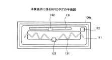
図1は、本実施例に係るRFIDタグ100aの平面図である。同図に示すように、RFIDタグ100aは、HF帯域用コイルアンテナ111と、HF帯域用RFIDチップ112と、UHF帯域用ダイポールアンテナ121と、UHF帯域用RFIDチップ122と、マイクロ波帯域用ダイポールアンテナ131と、マイクロ波帯域用RFIDチップ132とを有する。 FIG. 1 is a plan view of an
HF帯域用コイルアンテナ111は、RFIDチップ内の回路動作と信号を送信するための電力をリーダライタから発する電磁界を受けて、電磁誘導により起電する機能を持っていると同時に、タグからの電磁信号による送受信を実現する機能を持つものである。HF帯域用RFIDチップ112は、HF帯域用コイルアンテナ111を介しての通信を制御するとともに、所定の情報を記憶する不揮発メモリ回路を備えたICチップである。本実施例では、リーダライタとタグ間での通信で使用される電磁界の周波数は13.56MHzであり、タグアンテナの共進周波数は13.56MHzに調整している。 The coil antenna for
UHF帯域用アンテナ121は、UHF帯域の電波を送受信するのに適した形状のダイポールアンテナであり、UHF帯域用RFIDチップ122は、UHF帯域用ダイポールアンテナ121を介してリーダライタとの通信を制御するとともに、所定の情報を記憶する不揮発メモリを内蔵したICチップである。このダイポールアンテナは950−956MHz帯域の電波長を考慮した長さとしており、この電波帯域では、電波の送受信に十分必要なアンテナゲインとなるように設計している。 The
マイクロ波帯域用ダイポールアンテナ131は、マイクロ波帯域の電磁波を送受信するのに適した形状のダイポールアンテナであり、マイクロ波帯域用RFIDチップ132は、マイクロ波帯域用ダイポールアンテナ131を介しての通信を制御するとともに、所定の情報を記憶する不揮発メモリを内蔵したICチップである。 The microwave
このように、RFIDタグ100aは、HF帯域用コイルアンテナ111と、UHF帯域用ダイポールアンテナ121と、マイクロ波帯域用ダイポールアンテナ131という3つのアンテナを有し、これらを並列に配置せず、同一タグ内に重ねて配置することによってサイズが大きくなることを回避している。 As described above, the
このように複数のアンテナを重ねて配置した場合、アンテナ同士の干渉やカップリングによってアンテナが機能しなくなる恐れがある。アンテナ間のスペースが近接しすぎると、アンテナ間の電気的結合により、結合性容量がアンテナの容量として見えるため、UHF帯やマイクロ波帯のアンテナでは、あらかじめチューニングしたインピーダンスから大きくずれ、チップ側回路へ電力を十分に供給できずに、タグの通信特性の劣化、或いは通信応答しない場合もある。また、HF帯では、アンテナの共振周波数がずれ、リーダライタとの通信性能が著しく低下する場合もあるが、本実施例に係るRFIDタグ100aは、アンテナ間に絶縁性のスペーサを配置することで、この問題を解決している。 When a plurality of antennas are arranged in such a manner, the antennas may not function due to interference or coupling between the antennas. If the space between the antennas is too close, the coupling capacitance appears as the antenna capacitance due to the electrical coupling between the antennas. Therefore, the UHF band and microwave band antennas deviate greatly from the impedance tuned in advance, and the chip side circuit In some cases, sufficient power cannot be supplied to the tag, the communication characteristics of the tag deteriorate, or no communication response is made. In the HF band, the resonance frequency of the antenna may be shifted and the communication performance with the reader / writer may be significantly degraded. However, the
図2は、本実施例に係るRFIDタグ100aの断面図である。同図に示すように、RFIDタグ100aは、HF帯域用コイルアンテナ111とUHF帯域用ダイポールアンテナ121の間と、HF帯域用コイルアンテナ111とマイクロ波帯域用ダイポールアンテナ131の間にスペーサ140を配置している。 FIG. 2 is a cross-sectional view of the
このスペーサ140は、電磁波の干渉を回避するために、絶縁性と所定の厚みを必要とする。スペーサ140の素材は、たとえば、ポリエチレンテレフタレート(PET)などの樹脂を利用することができる。スペーサ140の素材を樹脂とした場合、2mm以上の厚さがあれば電磁波の干渉を回避することができる。スペーサ140の素材は、樹脂以外に、たとえば、セラミックや絶縁紙などであってもよい。また、今回の実施例では、スペーサにより確保されるスペース厚みを2mmとしているが、スペーサ材の誘電率を変化させることにより、その厚みも制御することができる。すなわち、誘電率を小さくすることにより、スペース厚みを薄くできる。 The
電磁波の干渉を回避するには、スペーサを使用する手法以外に、アンテナをコーティングする手法も有効である。図3は、コーティングにより電磁波干渉を回避する場合のRFIDタグ100bの断面図である。RFIDタグ100bは、本実施例に係るRFIDタグ100aと同様のアンテナを内蔵したRFIDタグである。 In order to avoid interference of electromagnetic waves, in addition to the method using a spacer, a method of coating an antenna is also effective. FIG. 3 is a cross-sectional view of the
同図に示すように、HF帯域用コイルアンテナ111は、コーティング150を施されており、UHF帯域用ダイポールアンテナ121やマイクロ波帯域用ダイポールアンテナ131と直接接触しないようになっている。このコーティングの素材は、HF帯域用コイルアンテナ111が送受信する周波数帯域の電磁波を透過させ、他の周波数帯域の電磁波は遮蔽する特性をもつ。 As shown in the figure, the HF
上述してきたように、本実施例では、RFIDタグ内に、それぞれの周波数帯域に適した形状のアンテナを重ねて配置し、スペーサやコーティングによって電磁波の干渉を回避するように構成したので、複数の周波数帯域に対応し、小型で十分な通信性能を発揮するRFIDタグを提供することができる。 As described above, in this embodiment, antennas having shapes suitable for the respective frequency bands are arranged in the RFID tag so as to avoid interference of electromagnetic waves by spacers and coatings. It is possible to provide an RFID tag that is small and exhibits sufficient communication performance in response to a frequency band.
また、このようにRFIDタグ内に複数のアンテナ及びRFIDチップを備えることで動作不良に対する二重化対策がとられることとなり、信頼性も向上する。 In addition, by providing a plurality of antennas and RFID chips in the RFID tag in this way, a countermeasure against duplication against malfunction is taken, and reliability is improved.
なお、本実施例ではアンテナごとにRFIDチップを備えた構成としているが、複数のアンテナが一つのRFIDチップを共用する構成とすることもできる。 In this embodiment, each antenna has an RFID chip. However, a plurality of antennas may share one RFID chip.
以上のように、本発明に係るRFIDタグおよびアンテナ配置方法は、複数の周波数帯への対応が必要な場合に有用であり、特に、小型で十分な性能を発揮するRFIDタグが必要な場合に適している。 As described above, the RFID tag and the antenna arrangement method according to the present invention are useful when it is necessary to cope with a plurality of frequency bands, and particularly when a small RFID tag that exhibits sufficient performance is required. Is suitable.
100a、100b RFIDタグ
111 HF帯域用コイルアンテナ
112 HF帯域用RFIDチップ
121 UHF帯域用ダイポールアンテナ
122 UHF帯域用RFIDチップ
131 マイクロ波帯域用ダイポールアンテナ
132 マイクロ波帯域用RFIDチップ
140 スペーサ
150 コーティング100a,
Claims (10)
Translated fromJapaneseアンテナ間の干渉を防止する干渉防止手段
を備えたことを特徴とするRFIDタグ。An RFID tag having a plurality of antennas,
An RFID tag comprising interference prevention means for preventing interference between antennas.
Priority Applications (2)
| Application Number | Priority Date | Filing Date | Title |
|---|---|---|---|
| JP2005116142AJP2006295729A (en) | 2005-04-13 | 2005-04-13 | RFID tag and antenna arrangement method |
| US11/283,921US20060232419A1 (en) | 2005-04-13 | 2005-11-22 | RFID tag and antenna arranging method |
Applications Claiming Priority (1)
| Application Number | Priority Date | Filing Date | Title |
|---|---|---|---|
| JP2005116142AJP2006295729A (en) | 2005-04-13 | 2005-04-13 | RFID tag and antenna arrangement method |
Publications (1)
| Publication Number | Publication Date |
|---|---|
| JP2006295729Atrue JP2006295729A (en) | 2006-10-26 |
Family
ID=37107981
Family Applications (1)
| Application Number | Title | Priority Date | Filing Date |
|---|---|---|---|
| JP2005116142AWithdrawnJP2006295729A (en) | 2005-04-13 | 2005-04-13 | RFID tag and antenna arrangement method |
Country Status (2)
| Country | Link |
|---|---|
| US (1) | US20060232419A1 (en) |
| JP (1) | JP2006295729A (en) |
Cited By (12)
| Publication number | Priority date | Publication date | Assignee | Title |
|---|---|---|---|---|
| EP1956524A2 (en) | 2007-02-09 | 2008-08-13 | Semiconductor Energy Laboratory Co., Ltd. | Semiconductor device |
| JP2008253500A (en)* | 2007-04-04 | 2008-10-23 | Toshiba Corp | Ultrasonic diagnostic apparatus, control processing program thereof, and ultrasonic probe |
| JP2009043167A (en)* | 2007-08-10 | 2009-02-26 | Nippon Electronics Service Kk | Composite rfid data carrier |
| JP2009288874A (en)* | 2008-05-27 | 2009-12-10 | Mitsubishi Electric Corp | Radio communication apparatus |
| WO2010001837A1 (en)* | 2008-07-02 | 2010-01-07 | 三菱電機株式会社 | Radio communication device |
| JP2011170714A (en)* | 2010-02-19 | 2011-09-01 | Taketomo:Kk | Packaging container |
| JP4843103B2 (en)* | 2008-07-02 | 2011-12-21 | 三菱電機株式会社 | Wireless communication device |
| JP2012016062A (en)* | 2008-07-02 | 2012-01-19 | Mitsubishi Electric Corp | Radio communication device |
| KR101151444B1 (en) | 2011-12-29 | 2012-06-08 | 김원기 | Integrated smart card |
| KR101277556B1 (en) | 2009-06-26 | 2013-06-24 | 미쓰비시덴키 가부시키가이샤 | Radio communication device |
| WO2023286352A1 (en)* | 2021-07-16 | 2023-01-19 | 大王製紙株式会社 | Antenna module and ic card |
| JP2024501241A (en)* | 2021-01-05 | 2024-01-11 | ベクトン ディキンソン フランス | Medical containers, systems and methods for tracking data related to such medical containers |
Families Citing this family (45)
| Publication number | Priority date | Publication date | Assignee | Title |
|---|---|---|---|---|
| JP4463574B2 (en)* | 2004-01-23 | 2010-05-19 | 株式会社リコー | IC tag reader / writer and apparatus having IC tag reader / writer |
| KR100843887B1 (en)* | 2006-06-02 | 2008-07-03 | 주식회사 하이닉스반도체 | Integrated circuits and information recording methods |
| US7659857B2 (en)* | 2006-07-05 | 2010-02-09 | King Patrick F | System and method for providing a low and narrow-profile radio frequency identification (RFID) tag |
| US9022293B2 (en) | 2006-08-31 | 2015-05-05 | Semiconductor Energy Laboratory Co., Ltd. | Semiconductor device and power receiving device |
| US20080079587A1 (en)* | 2006-09-29 | 2008-04-03 | Ahmadreza Rofougaran | Method And System For Utilizing Magnetic On-Chip Coil For Ultra High Frequency (UHF) |
| US8165552B2 (en)* | 2006-09-29 | 2012-04-24 | Broadcom Corporation | Method and system for identifying radio frequency identification (RFID) tag location using a switchable coil |
| US8031651B2 (en) | 2006-09-29 | 2011-10-04 | Broadcom Corporation | Method and system for minimizing power consumption in a communication system |
| US8264366B2 (en)* | 2009-03-31 | 2012-09-11 | Corning Incorporated | Components, systems, and methods for associating sensor data with component location |
| US8421626B2 (en)* | 2006-10-31 | 2013-04-16 | Corning Cable Systems, Llc | Radio frequency identification transponder for communicating condition of a component |
| US9652707B2 (en) | 2006-10-31 | 2017-05-16 | Fiber Mountain, Inc. | Radio frequency identification (RFID) connected tag communications protocol and related systems and methods |
| US10032102B2 (en) | 2006-10-31 | 2018-07-24 | Fiber Mountain, Inc. | Excess radio-frequency (RF) power storage in RF identification (RFID) tags, and related systems and methods |
| US9652709B2 (en) | 2006-10-31 | 2017-05-16 | Fiber Mountain, Inc. | Communications between multiple radio frequency identification (RFID) connected tags and one or more devices, and related systems and methods |
| US9652708B2 (en) | 2006-10-31 | 2017-05-16 | Fiber Mountain, Inc. | Protocol for communications between a radio frequency identification (RFID) tag and a connected device, and related systems and methods |
| US7772975B2 (en) | 2006-10-31 | 2010-08-10 | Corning Cable Systems, Llc | System for mapping connections using RFID function |
| US7782202B2 (en) | 2006-10-31 | 2010-08-24 | Corning Cable Systems, Llc | Radio frequency identification of component connections |
| US8264355B2 (en) | 2006-12-14 | 2012-09-11 | Corning Cable Systems Llc | RFID systems and methods for optical fiber network deployment and maintenance |
| US7667574B2 (en)* | 2006-12-14 | 2010-02-23 | Corning Cable Systems, Llc | Signal-processing systems and methods for RFID-tag signals |
| US7760094B1 (en) | 2006-12-14 | 2010-07-20 | Corning Cable Systems Llc | RFID systems and methods for optical fiber network deployment and maintenance |
| US7965186B2 (en) | 2007-03-09 | 2011-06-21 | Corning Cable Systems, Llc | Passive RFID elements having visual indicators |
| US7547150B2 (en) | 2007-03-09 | 2009-06-16 | Corning Cable Systems, Llc | Optically addressed RFID elements |
| US7855697B2 (en)* | 2007-08-13 | 2010-12-21 | Corning Cable Systems, Llc | Antenna systems for passive RFID tags |
| US8248208B2 (en) | 2008-07-15 | 2012-08-21 | Corning Cable Systems, Llc. | RFID-based active labeling system for telecommunication systems |
| WO2010018546A1 (en)* | 2008-08-13 | 2010-02-18 | Ipico Innovation Inc | A dual frequency rfid tag |
| US8731405B2 (en) | 2008-08-28 | 2014-05-20 | Corning Cable Systems Llc | RFID-based systems and methods for collecting telecommunications network information |
| US8068012B2 (en)* | 2009-01-08 | 2011-11-29 | Intelleflex Corporation | RFID device and system for setting a level on an electronic device |
| EP2507746B1 (en) | 2009-11-30 | 2015-10-14 | Corning Incorporated | Rfid condition latching |
| US9122967B2 (en) | 2010-04-14 | 2015-09-01 | Technologies Roi, Llc | Radio frequency identification tags and methods employing ceramic components, which may be suitable for use in extreme environmental conditions |
| US8172468B2 (en) | 2010-05-06 | 2012-05-08 | Corning Incorporated | Radio frequency identification (RFID) in communication connections, including fiber optic components |
| CN102918550B (en)* | 2010-05-17 | 2016-08-10 | Zih公司 | Double response device RF identification |
| TWI446271B (en)* | 2010-09-14 | 2014-07-21 | Icon Minsky Luo | Near field communication device, authentication system using the same and method thereof |
| US20130062418A1 (en)* | 2011-04-06 | 2013-03-14 | Craig WEAKLEY | Rfid tag having coupled resonator loop with loading |
| CN102955974B (en)* | 2011-08-29 | 2016-01-20 | 奇鋐科技股份有限公司 | Smart Card with stand-alone display |
| US9152912B2 (en)* | 2011-10-13 | 2015-10-06 | Asia Vital Components Co., Ltd. | Smart card capable of independently displaying information |
| TWI453677B (en)* | 2011-12-01 | 2014-09-21 | Mutual Pak Technology Co Ltd | Radio frequency identification tag and cloth having the same |
| EP2629235B1 (en) | 2012-02-17 | 2016-04-13 | ams AG | RFID, reader, RFID network and method for communication in an RFID network |
| US9165232B2 (en) | 2012-05-14 | 2015-10-20 | Corning Incorporated | Radio-frequency identification (RFID) tag-to-tag autoconnect discovery, and related methods, circuits, and systems |
| US20140048524A1 (en)* | 2012-08-20 | 2014-02-20 | Lincoln Global, Inc. | Hot-wire consumable with embedded id tag |
| US9563832B2 (en) | 2012-10-08 | 2017-02-07 | Corning Incorporated | Excess radio-frequency (RF) power storage and power sharing RF identification (RFID) tags, and related connection systems and methods |
| EP2930680A4 (en)* | 2012-12-04 | 2016-08-03 | Nec Corp | Product management system, product management method, and non-temporary computer-readable medium for storing product management program |
| US9734445B2 (en)* | 2013-09-27 | 2017-08-15 | Infineon Technologies Ag | Electronic document with two antennas |
| US10158166B2 (en)* | 2014-11-06 | 2018-12-18 | Leonardo S.P.A. | Eco-friendly thermoplastic conformal coating for antenna array systems |
| JP6699660B2 (en)* | 2015-04-27 | 2020-05-27 | 日本電気株式会社 | UHF band RFID system and UHF band RFID tag detection method |
| CN111355013A (en)* | 2018-12-20 | 2020-06-30 | 夏敬懿 | Anti-jamming antenna board |
| EP3839826B1 (en)* | 2019-12-20 | 2022-08-10 | Assa Abloy AB | Rfid assembly |
| JP7518356B2 (en)* | 2020-06-16 | 2024-07-18 | 株式会社デンソーウェーブ | Interference suppression device and interference suppression system |
Family Cites Families (3)
| Publication number | Priority date | Publication date | Assignee | Title |
|---|---|---|---|---|
| US6975834B1 (en)* | 2000-10-03 | 2005-12-13 | Mineral Lassen Llc | Multi-band wireless communication device and method |
| US7050017B2 (en)* | 2002-08-14 | 2006-05-23 | King Patrick F | RFID tire belt antenna system and method |
| US6940408B2 (en)* | 2002-12-31 | 2005-09-06 | Avery Dennison Corporation | RFID device and method of forming |
- 2005
- 2005-04-13JPJP2005116142Apatent/JP2006295729A/ennot_activeWithdrawn
- 2005-11-22USUS11/283,921patent/US20060232419A1/ennot_activeAbandoned
Cited By (17)
| Publication number | Priority date | Publication date | Assignee | Title |
|---|---|---|---|---|
| EP1956524A2 (en) | 2007-02-09 | 2008-08-13 | Semiconductor Energy Laboratory Co., Ltd. | Semiconductor device |
| US8552921B2 (en) | 2007-02-09 | 2013-10-08 | Semiconductor Energy Laboratory Co., Ltd. | Semiconductor device |
| US7940224B2 (en) | 2007-02-09 | 2011-05-10 | Semiconductor Energy Laboratory Co., Ltd. | Semiconductor device |
| JP2008253500A (en)* | 2007-04-04 | 2008-10-23 | Toshiba Corp | Ultrasonic diagnostic apparatus, control processing program thereof, and ultrasonic probe |
| JP2009043167A (en)* | 2007-08-10 | 2009-02-26 | Nippon Electronics Service Kk | Composite rfid data carrier |
| JP2009288874A (en)* | 2008-05-27 | 2009-12-10 | Mitsubishi Electric Corp | Radio communication apparatus |
| JP2012016062A (en)* | 2008-07-02 | 2012-01-19 | Mitsubishi Electric Corp | Radio communication device |
| JP4843103B2 (en)* | 2008-07-02 | 2011-12-21 | 三菱電機株式会社 | Wireless communication device |
| KR101201441B1 (en) | 2008-07-02 | 2012-11-14 | 미쓰비시덴키 가부시키가이샤 | Radio communication device |
| US8508429B2 (en) | 2008-07-02 | 2013-08-13 | Mitsubishi Electric Corporation | Radio communication equipment |
| WO2010001837A1 (en)* | 2008-07-02 | 2010-01-07 | 三菱電機株式会社 | Radio communication device |
| KR101277556B1 (en) | 2009-06-26 | 2013-06-24 | 미쓰비시덴키 가부시키가이샤 | Radio communication device |
| JP2011170714A (en)* | 2010-02-19 | 2011-09-01 | Taketomo:Kk | Packaging container |
| KR101151444B1 (en) | 2011-12-29 | 2012-06-08 | 김원기 | Integrated smart card |
| JP2024501241A (en)* | 2021-01-05 | 2024-01-11 | ベクトン ディキンソン フランス | Medical containers, systems and methods for tracking data related to such medical containers |
| WO2023286352A1 (en)* | 2021-07-16 | 2023-01-19 | 大王製紙株式会社 | Antenna module and ic card |
| JP2023013724A (en)* | 2021-07-16 | 2023-01-26 | 大王製紙株式会社 | Antenna module and IC card |
Also Published As
| Publication number | Publication date |
|---|---|
| US20060232419A1 (en) | 2006-10-19 |
Similar Documents
| Publication | Publication Date | Title |
|---|---|---|
| JP2006295729A (en) | RFID tag and antenna arrangement method | |
| US7696884B2 (en) | Systems and methods for enhancing the magnetic coupling in a wireless communication system | |
| EP2071495B1 (en) | Wireless ic device | |
| JP4578411B2 (en) | Antenna and wireless tag | |
| JP5429182B2 (en) | Wireless IC device | |
| US20070222603A1 (en) | Systems and methods for enhancing communication in a wireless communication system | |
| CN101346852B (en) | Wireless IC device | |
| JP5835360B2 (en) | ANTENNA DEVICE, CARD-TYPE COMMUNICATION DEVICE, AND COMMUNICATION TERMINAL DEVICE | |
| US9865913B2 (en) | Communication terminal and card antenna module | |
| JP2006042059A (en) | Radio communication apparatus and impedance controlling method thereof | |
| KR20100027205A (en) | Antenna for rfid reader/writer | |
| JP5094630B2 (en) | IC tag | |
| JP4409257B2 (en) | Radio tag, article provided with the same, and RFID system | |
| US8899489B2 (en) | Resonant circuit structure and RF tag having same | |
| JP2011095844A (en) | Noncontact electronic device | |
| KR100867853B1 (en) | RFID antennas and RDF tags | |
| KR100951138B1 (en) | Miniature Wideband RDF Tag Antenna | |
| JP2005236468A (en) | Wireless tag | |
| CN101783441A (en) | Antenna device and radio frequency device | |
| KR100862477B1 (en) | RFID tag | |
| KR20080042252A (en) | RFID antennas and RDF tags | |
| JP4859020B2 (en) | Wireless tag device | |
| US20240195048A1 (en) | Near field communication antenna | |
| KR20080065405A (en) | RFID tag | |
| JP6518904B1 (en) | Wireless communication terminal |
Legal Events
| Date | Code | Title | Description |
|---|---|---|---|
| A621 | Written request for application examination | Free format text:JAPANESE INTERMEDIATE CODE: A621 Effective date:20071221 | |
| A761 | Written withdrawal of application | Free format text:JAPANESE INTERMEDIATE CODE: A761 Effective date:20080417 |