JP2006294866A - Semiconductor device - Google Patents
Semiconductor deviceDownload PDFInfo
- Publication number
- JP2006294866A JP2006294866AJP2005113483AJP2005113483AJP2006294866AJP 2006294866 AJP2006294866 AJP 2006294866AJP 2005113483 AJP2005113483 AJP 2005113483AJP 2005113483 AJP2005113483 AJP 2005113483AJP 2006294866 AJP2006294866 AJP 2006294866A
- Authority
- JP
- Japan
- Prior art keywords
- electrode
- semiconductor device
- elastic member
- substrate
- piezoelectric actuator
- Prior art date
- Legal status (The legal status is an assumption and is not a legal conclusion. Google has not performed a legal analysis and makes no representation as to the accuracy of the status listed.)
- Abandoned
Links
Images


Classifications
- H—ELECTRICITY
- H01—ELECTRIC ELEMENTS
- H01G—CAPACITORS; CAPACITORS, RECTIFIERS, DETECTORS, SWITCHING DEVICES, LIGHT-SENSITIVE OR TEMPERATURE-SENSITIVE DEVICES OF THE ELECTROLYTIC TYPE
- H01G5/00—Capacitors in which the capacitance is varied by mechanical means, e.g. by turning a shaft; Processes of their manufacture
- H01G5/16—Capacitors in which the capacitance is varied by mechanical means, e.g. by turning a shaft; Processes of their manufacture using variation of distance between electrodes
- H01G5/18—Capacitors in which the capacitance is varied by mechanical means, e.g. by turning a shaft; Processes of their manufacture using variation of distance between electrodes due to change in inclination, e.g. by flexing, by spiral wrapping
- H—ELECTRICITY
- H01—ELECTRIC ELEMENTS
- H01H—ELECTRIC SWITCHES; RELAYS; SELECTORS; EMERGENCY PROTECTIVE DEVICES
- H01H59/00—Electrostatic relays; Electro-adhesion relays
- H01H59/0009—Electrostatic relays; Electro-adhesion relays making use of micromechanics
- H—ELECTRICITY
- H02—GENERATION; CONVERSION OR DISTRIBUTION OF ELECTRIC POWER
- H02N—ELECTRIC MACHINES NOT OTHERWISE PROVIDED FOR
- H02N1/00—Electrostatic generators or motors using a solid moving electrostatic charge carrier
- H02N1/002—Electrostatic motors
- H02N1/006—Electrostatic motors of the gap-closing type
- H—ELECTRICITY
- H10—SEMICONDUCTOR DEVICES; ELECTRIC SOLID-STATE DEVICES NOT OTHERWISE PROVIDED FOR
- H10N—ELECTRIC SOLID-STATE DEVICES NOT OTHERWISE PROVIDED FOR
- H10N30/00—Piezoelectric or electrostrictive devices
- H10N30/20—Piezoelectric or electrostrictive devices with electrical input and mechanical output, e.g. functioning as actuators or vibrators
- H10N30/204—Piezoelectric or electrostrictive devices with electrical input and mechanical output, e.g. functioning as actuators or vibrators using bending displacement, e.g. unimorph, bimorph or multimorph cantilever or membrane benders
- H10N30/2041—Beam type
- H10N30/2042—Cantilevers, i.e. having one fixed end
- H10N30/2043—Cantilevers, i.e. having one fixed end connected at their free ends, e.g. parallelogram type
- H—ELECTRICITY
- H01—ELECTRIC ELEMENTS
- H01H—ELECTRIC SWITCHES; RELAYS; SELECTORS; EMERGENCY PROTECTIVE DEVICES
- H01H1/00—Contacts
- H01H1/0036—Switches making use of microelectromechanical systems [MEMS]
- H01H2001/0063—Switches making use of microelectromechanical systems [MEMS] having electrostatic latches, i.e. the activated position is kept by electrostatic forces other than the activation force
- H—ELECTRICITY
- H01—ELECTRIC ELEMENTS
- H01H—ELECTRIC SWITCHES; RELAYS; SELECTORS; EMERGENCY PROTECTIVE DEVICES
- H01H57/00—Electrostrictive relays; Piezoelectric relays
- H01H2057/006—Micromechanical piezoelectric relay
- H—ELECTRICITY
- H01—ELECTRIC ELEMENTS
- H01H—ELECTRIC SWITCHES; RELAYS; SELECTORS; EMERGENCY PROTECTIVE DEVICES
- H01H59/00—Electrostatic relays; Electro-adhesion relays
- H01H59/0009—Electrostatic relays; Electro-adhesion relays making use of micromechanics
- H01H2059/0018—Special provisions for avoiding charge trapping, e.g. insulation layer between actuating electrodes being permanently polarised by charge trapping so that actuating or release voltage is altered
Landscapes
- Engineering & Computer Science (AREA)
- Power Engineering (AREA)
- Microelectronics & Electronic Packaging (AREA)
- Micromachines (AREA)
- Semiconductor Integrated Circuits (AREA)
Abstract
Translated fromJapaneseDescription
Translated fromJapaneseこの発明は、マイクロマシンもしくはMEMS(Micro-Electro-Mechanical Systems)技術を用いて形成した可変容量やスイッチなどの半導体装置に関する。 The present invention relates to a semiconductor device such as a variable capacitor and a switch formed by using a micromachine or MEMS (Micro-Electro-Mechanical Systems) technology.
MEMS技術を採用した可変容量やスイッチは、PINダイオードやFETを使用したものと比較してロスが少ない(Q値が大きい)、歪が少ないなどの利点を有する。このため、次世代携帯電話システムへの搭載が有望視されている。 Variable capacitors and switches that employ MEMS technology have advantages such as less loss (large Q value) and less distortion compared to those using PIN diodes or FETs. For this reason, it is considered promising for use in next-generation mobile phone systems.
これらMEMS可変容量とスイッチの駆動方式には、静電型、圧電型、熱型、電磁型などが用いられている。このうち熱型と電磁型は消費電力が大きく、携帯機器への搭載には向いていない。これに対し、静電型(例えば特許文献1参照)は消費電力が小さいものの、次のような欠点を持っている。 Electrostatic type, piezoelectric type, thermal type, electromagnetic type, etc. are used for the drive system of these MEMS variable capacitors and switches. Of these, the thermal type and the electromagnetic type consume a large amount of power and are not suitable for mounting on portable devices. On the other hand, the electrostatic type (see, for example, Patent Document 1) has the following drawbacks although the power consumption is small.
i) 駆動電圧が高い。 i) The drive voltage is high.
ii) 絶縁膜への電荷トラップによるスティッキングが発生する。 ii) Sticking occurs due to charge trapping in the insulating film.
電極間距離が約1μmのMEMS可変容量の場合、静電引力で電極を接触させるには約20Vの高電圧が必要となる。この電圧は携帯電話システムの電源電圧より高いため、高電圧を生成する部品もしくは回路が必要となりコストがかかる。また、高電圧を生成するために消費電力も増加する。静電型の可変容量やスイッチでは、この高電圧のために電極間の絶縁膜に電荷がトラップされることが知られている。一回のスイッチングでトラップされる電荷量はわずかであるが、スイッチングを繰り返すと多くの電荷が溜まり、プルアウト電圧がシフトする。このシフト量が大きくなると、電極がくっついたまま離れなくなる(スティッキング)。このスティッキングは106回以上のスイッチングで起こることが知られている。In the case of a MEMS variable capacitor having a distance between electrodes of about 1 μm, a high voltage of about 20 V is required to bring the electrodes into contact with each other by electrostatic attraction. Since this voltage is higher than the power supply voltage of the mobile phone system, a part or a circuit that generates a high voltage is required, which is expensive. In addition, the power consumption increases in order to generate a high voltage. In electrostatic variable capacitors and switches, it is known that charges are trapped in an insulating film between electrodes due to this high voltage. Although the amount of charge trapped by a single switching is small, a large amount of charge accumulates when switching is repeated, and the pull-out voltage shifts. When this shift amount is increased, the electrodes remain stuck and cannot be separated (sticking). This sticking is known to occur after switching 106 times or more.
一方、圧電型の可変容量やスイッチは5V以下の低電圧で駆動可能であり、消費電力も小さい。しかし、駆動力が弱いためコンタクト力が10μN程度と静電型の1/10であり、次のような問題が起こる。 On the other hand, piezoelectric variable capacitors and switches can be driven at a low voltage of 5 V or less, and power consumption is small. However, since the driving force is weak, the contact force is about 10 μN, which is 1/10 of the electrostatic type, and the following problems occur.
iii) MEMSスイッチの場合、接触抵抗が大きい。 iii) In the case of a MEMS switch, the contact resistance is large.
iv) MEMS可変容量の場合、電極間の密着性が悪い(電極に微小な凹凸や反りがあっても、駆動力が強いと電極間を密着させることができる。駆動力が弱いと密着させることができず、結果として可変幅が小さくなる)。 iv) In the case of a MEMS variable capacitor, the adhesion between the electrodes is poor (even if the electrodes have minute irregularities and warpage, the electrodes can be in close contact with each other if the driving force is strong. (As a result, the variable width becomes smaller).
このように、静電型や圧電型の可変容量やスイッチは、熱型や電磁型に比べて携帯機器への搭載には向いているものの、駆動電圧、スティッキング、接触抵抗、電極間の密着性などの特性や機能において一長一短があり、いずれも十分なものではなく改良が望まれている。
この発明の目的とするところは、小さな駆動電圧で大きなコンタクト力が得られる半導体装置を提供することにある。 An object of the present invention is to provide a semiconductor device capable of obtaining a large contact force with a small driving voltage.
この発明の一態様によると、基板との間に空隙を形成するように、一端がアンカーを介して固定され、変形されることによって他端と前記基板間の距離が変化する弾性部材と、前記弾性部材の他端に配置された第1の電極と、前記第1の電極と対向するように前記基板上に配置された第2の電極と、前記弾性部材内に配置され、前記弾性部材の他端を前記基板に近づけるように変形させる圧電アクチュエータと、前記弾性部材内に配置された第3の電極と、前記第3の電極と対向するように前記基板上に配置された第4の電極とからなり、前記弾性部材の他端を前記基板に近づけるように変形させる静電アクチュエータとを具備し、前記圧電アクチュエータと前記静電アクチュエータの駆動によって第1の電極と第2の電極との距離が変化する半導体装置が提供される。 According to one aspect of the present invention, one end is fixed via an anchor so as to form a gap between the substrate and the elastic member whose distance between the other end and the substrate changes when deformed, A first electrode disposed at the other end of the elastic member; a second electrode disposed on the substrate so as to face the first electrode; and disposed within the elastic member; A piezoelectric actuator that deforms the other end closer to the substrate, a third electrode disposed in the elastic member, and a fourth electrode disposed on the substrate so as to face the third electrode And an electrostatic actuator that deforms the other end of the elastic member so as to approach the substrate, and the distance between the first electrode and the second electrode by driving the piezoelectric actuator and the electrostatic actuator. Changes The semiconductor device is provided.
この発明によれば、小さな駆動電圧で大きなコンタクト力が得られる半導体装置が得られる。 According to the present invention, a semiconductor device capable of obtaining a large contact force with a small driving voltage can be obtained.
以下、この発明の実施の形態について図面を参照して説明する。
[第1の実施形態]
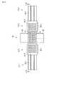
図1乃至図3はそれぞれ、この発明の第1の実施形態に係る半導体装置について説明するためのもので、図1は可変容量の平面図、図2は図1のII−II’線に沿った断面図、図3は図1のIII−III’線に沿った断面図である。この半導体装置は、可変容量部11、静電アクチュエータ部12−1,12−2及び圧電アクチュエータ部13−1,13−2を含んで構成されている。上記圧電アクチュエータ部13−1、静電アクチュエータ部12−1、可変容量部11、静電アクチュエータ部12−2及び圧電アクチュエータ部13−2は一方向に沿って直線的に配置されている。これらは基板(例えばシリコン基板)10上にアンカー27−1,27−2で弾性部材15の両端が固定された構造体中に形成される。上記弾性部材15と基板10との間には空洞35が形成されており、上記圧電アクチュエータ部13−1,13−2と上記静電アクチュエータ部12−1,12−2とを駆動することによって上記弾性部材15の中央部(可変容量部11)が基板10に近づくように変形し、上記弾性部材15と基板10との間の距離が変化するようになっている。Embodiments of the present invention will be described below with reference to the drawings.
[First Embodiment]
1 to 3 are diagrams for explaining a semiconductor device according to the first embodiment of the present invention. FIG. 1 is a plan view of a variable capacitor, and FIG. 2 is taken along the line II-II ′ of FIG. FIG. 3 is a sectional view taken along the line III-III ′ of FIG. This semiconductor device includes a
すなわち、上記可変容量部11は、弾性部材15中に形成された上部電極21と基板10上に形成された下部電極22,23とを備えている。上部電極21はフロートとなっており、上記アクチュエータ部12−1,12−2,13−1,13−2で駆動されることにより電極間距離が変化する。上記可変容量部11の上部電極21がアクチュエータ部12−1,12−2,13−1,13−2により下げられると、この上部電極21が下部電極22,23に近づく。これにより、下部電極22,23が容量結合する。上部電極21が上がっている状態では、上部電極21と絶縁膜33の間に約1.5μmの隙間ができる。従って、この状態では下部電極22,23の間の容量は無視できるほど小さくなる。このように、上部電極21を上下動することにより、容量値が2値的に変化するデジタル可変容量を形成できる。 That is, the
次に、上記可変容量部11の電極間距離を制御するハイブリッド型のアクチュエータについて説明する。上記静電アクチュエータ部12−1,12−2はそれぞれ、上記可変容量部11の両側に配置され、上部電極25−1,25−2と下部電極26−1,26−2とで構成されている。これら静電アクチュエータ部12−1,12−2と両端のアンカー27−1,27−2との間にはそれぞれ、上記圧電アクチュエータ部13−1,13−2が設けられている。上記圧電アクチュエータ部13−1,13−2は、圧電膜28−1,28−2、及びこれら圧電膜28−1,28−2をそれぞれ挟むように配置された圧電駆動用の上部電極29−1,29−2と下部電極30−1,30−2とを有している。上記圧電膜28−1,28−2の材料としては、例えばAlN,PZTなどを使用する。 Next, a hybrid actuator that controls the distance between the electrodes of the
上記可変容量部11の上部電極21、上記静電アクチュエータ部12−1,12−2の上部電極25−1,25−2、及び圧電アクチュエータ部13−1,13−2の上部電極29−1,29−2上には絶縁膜31が形成されている。上記圧電アクチュエータ部13−1,13−2の下部電極30−1,30−2下には絶縁膜32が形成されている。また、上記可変容量部11の下部電極22,23及び上記静電アクチュエータ部12−1,12−2の下部電極26−1,26−2は、基板10上に形成された絶縁膜34上に形成される。これらの下部電極22,23,26−1,26−2上には絶縁膜33が形成されている。 The
上記のような構成において、圧電アクチュエータ部13−1,13−2における上部電極29−1,29−2と下部電極30−1,30−2間に電位差をかけると、圧電膜28−1,28−2が変位して、弾性部材15の他端が下方に変位する。この圧電アクチュエータ部13−1,13−2には、ユニモルフ型とバイモルフ型のいずれも用いることができる。上記圧電アクチュエータ部13−1,13−2の上部電極29−1,29−2と下部電極30−1,30−2間に第1の電位差をかけて上部電極21,25−1,25−2を下方に変位させたとき、上部電極25−1,25−2と下部電極26−1,26−2とが近づく。次いで、この状態で、上部電極25−1,25−2と下部電極26−1,26−2の間に第2の電位差を印加する。この第2の電位差は上記第1の電位差と同じでも良く、あるいは第1の電位差よりも小さくても大きくても良い。これによって、可変容量部11の上部電極21が下方に変位し、上部電極21と下部電極22,23間の電極間距離が小さくなって容量値が2値的に変化する。 In the above configuration, when a potential difference is applied between the upper electrodes 29-1, 29-2 and the lower electrodes 30-1, 30-2 in the piezoelectric actuator portions 13-1, 13-2, the piezoelectric films 28-1, 28-2 is displaced, and the other end of the
可変容量部11の上部電極21を上方に変位させて戻すには、静電アクチュエータ部12−1,12−2の電位差をなくしたあと、もしくはそれと同時に圧電アクチュエータ部13−1,13−2の電位差をなくせば良い。 In order to displace the
上記のような構成では、圧電アクチュエータ部13−1,13−2は変位量が大きいため、第1の電位差は5V以下でも動作可能である。通常、静電アクチュエータ部12−1,12−2を駆動するには20V以上の高い電位差が必要であるが、本実施形態の場合、圧電アクチュエータ部13−1,13−2を駆動して極板間距離(電極間距離)が短くなった状態で静電アクチュエータ部12−1,12−2を駆動する。静電引力は極板間距離の逆数の二乗に比例するため、電極間の電位差が第1の電位差以下であっても十分強い静電引力が得られ、可変容量部11の上部電極21と下部電極22,23の高い密着性を確保できる。 In the configuration as described above, since the piezoelectric actuator units 13-1 and 13-2 have a large displacement, they can operate even when the first potential difference is 5 V or less. Normally, a high potential difference of 20 V or more is required to drive the electrostatic actuator units 12-1 and 12-2. In the case of this embodiment, the piezoelectric actuator units 13-1 and 13-2 are driven to generate poles. The electrostatic actuator units 12-1 and 12-2 are driven in a state where the distance between the plates (distance between the electrodes) is shortened. Since the electrostatic attractive force is proportional to the square of the reciprocal of the distance between the electrode plates, a sufficiently strong electrostatic attractive force can be obtained even if the potential difference between the electrodes is equal to or less than the first potential difference. High adhesion of the
また、本実施形態の構成では、静電アクチュエータ部12−1,12−2の極板間電位差が小さいため、絶縁膜33への電荷トラップが起こり難い。このため、従来技術よりスイッチング回数を増やすことができる。 Further, in the configuration of the present embodiment, since the potential difference between the electrode plates of the electrostatic actuator units 12-1 and 12-2 is small, charge trapping on the insulating
しかも、図1の可変容量部11及び静電アクチュエータ部12−1,12−2にマトリックス状に形成されている窓14は、空洞35を形成するためのエッチング工程において、エッチングの進行を均一化するためのものであるが、空気抵抗の削減にも寄与し、高速スイッチングが可能になる。勿論、この窓14は必須ではなく、なくてもこの発明の本質的な効果に変わりはない。 In addition, the
なお、本実施形態では、静電アクチュエータ部12−1,12−2の圧電駆動用下部電極30−1,30−2と、静電アクチュエータ部12−1,12−2の上部電極25−1,25−2とをショート(接続)しているが、圧電駆動用の上部電極29−1,29−2と静電アクチュエータ部12−1,12−2の上部電極25−1,25−2とをショートさせる構成でも実質的に同様な作用効果が得られる。また、静電アクチュエータ部12−1,12−2の上部電極25−1,25−2と下部電極30−1,30−2は別々に制御しても良い。 In the present embodiment, the piezoelectric driving lower electrodes 30-1 and 30-2 of the electrostatic actuator units 12-1 and 12-2 and the upper electrode 25-1 of the electrostatic actuator units 12-1 and 12-2. , 25-2 are short-circuited (connected), but the upper electrodes 29-1, 29-2 for driving the piezoelectric and the upper electrodes 25-1, 25-2 of the electrostatic actuator units 12-1, 12-2. Even in the configuration in which the two are short-circuited, substantially the same effect can be obtained. Further, the upper electrodes 25-1, 25-2 and the lower electrodes 30-1, 30-2 of the electrostatic actuator units 12-1, 12-2 may be controlled separately.
上述した本実施形態の可変容量は、携帯機器、例えば地上デジタル放送視聴可能な携帯電話のアンテナ整合回路への使用に適している。以下この適用例を説明する。 The above-described variable capacitor of the present embodiment is suitable for use in an antenna matching circuit of a mobile device, for example, a mobile phone capable of viewing digital terrestrial broadcasting. This application example will be described below.
図4は、地上デジタル放送視聴機能を搭載した携帯電話のブロック図である。図4におけるバックエンドシステム41は、従来の携帯電話に備わっているシステムである。地上デジタル放送視聴のために新規に追加しているのは、地上デジタル放送受信専用アンテナ42、整合回路システム43、及びチューナ44とOFDM復調LSI45からなるフロントシステム46である。上記整合回路システム43はアンテナの不整合損による狭帯域化を防ぐ役割を担っており、ドライバ47と整合回路48を備えている。 FIG. 4 is a block diagram of a mobile phone equipped with a digital terrestrial broadcast viewing function. The
次に、上記整合回路システム43についてより詳しく説明する。 Next, the
地上デジタル放送は、周波数470−770MHz(波長63cm−39cm)のUHF帯の電波を用いて放送される。電波の波長が長いため、ダイポールアンテナでこの地上デジタル放送を受信しようとすると、約15cmの長さのアンテナが必要となる。しかし、近年の携帯電話ではデザイン性が特に重視されるため、アンテナの長さは極力短いことが要求されている。可能であれば、アンテナを携帯電話の筐体内に内蔵させることが望ましい。しかしながら、単にアンテナを小型化すると帯域が狭くなり、周波数470−770MHzの全てを受信できなくなる。そこで、この問題を回避するために整合回路48を設け、見たい番組に応じて整合周波数を変化させている。この整合回路48は、例えば可変容量により構成し、可変容量の容量値を変化させることにより整合周波数を変えるように構成すれば良い。 Terrestrial digital broadcasting is broadcast using UHF radio waves having a frequency of 470-770 MHz (wavelength 63 cm-39 cm). Since the wavelength of the radio wave is long, when trying to receive this terrestrial digital broadcast with a dipole antenna, an antenna having a length of about 15 cm is required. However, in recent mobile phones, since design is particularly important, the length of the antenna is required to be as short as possible. If possible, it is desirable to incorporate the antenna in the casing of the mobile phone. However, if the antenna is simply reduced in size, the band becomes narrower and it becomes impossible to receive all of the frequencies 470-770 MHz. In order to avoid this problem, a matching
アンテナを小型化する場合のもう1つの問題点は、アンテナ効率の低下である。アンテナ効率はアンテナ自身の放射抵抗と、アンテナから受信回路に至るまでの損失抵抗とで決まり、
アンテナ効率=放射抵抗/(放射抵抗+損失抵抗)
と表される。アンテナを小型化すると放射抵抗が小さくなるため、損失抵抗が小さくならない限りアンテナ効率が低下する。例えば整合回路48の可変容量としてPINダイオードを採用すると、損失抵抗が大きいためアンテナ効率が低下してしまう。これに対し、MEMSは損失抵抗が小さく、1Ω以下に抑えることも可能である。従って、整合回路48にMEMS可変容量を採用すれば、小型アンテナを実現でき、携帯電話の筐体内にアンテナを内蔵することも可能となる。Another problem in miniaturizing the antenna is a decrease in antenna efficiency. Antenna efficiency is determined by the radiation resistance of the antenna itself and the loss resistance from the antenna to the receiving circuit.
Antenna efficiency = radiation resistance / (radiation resistance + loss resistance)
It is expressed. When the antenna is downsized, the radiation resistance is reduced, so that the antenna efficiency is lowered unless the loss resistance is reduced. For example, when a PIN diode is employed as the variable capacitor of the matching
上述したような考察に基づき、図4の整合回路システム43における整合回路48は、図1乃至図3に示した半導体装置(可変容量)で構成されている。バックエンドシステム41のコントローラ49から出力された選局情報はドライバ47、チューナ44及びOFDM復調LSI45に入力される。上記ドライバ47に入力された選局情報は、容量値選択信号CSSに変換されたのち整合回路48に入力される。 Based on the above consideration, the matching
図5は、上記図4に示した回路におけるドライバ47の具体的な構成例を示す回路図である。選局情報はバイナリの信号形態であり、例えばI2Cバスを介してドライバ47に入力される。このバイナリ信号はドライバ47内のデコーダ(Decoder)51でデコードされる。このデコーダ51から出力されるデコード信号Si(i=1,…,n)が活性化されると(例えば“High”/“Low”のうちの“High”状態になる)、スイッチSWiがオンしてi番目のヒューズデータfuse−iが容量値選択信号CSSとして出力され、整合回路48に入力される。このようにして、選局情報に応じて整合回路48の容量値が変化し、選局された放送局の周波数帯にアンテナの整合がとれた状態にできる。FIG. 5 is a circuit diagram showing a specific configuration example of the
上記容量値選択信号CSSとしてヒューズデータfuse−i(i=1,…,n)を使用するのは、MEMS可変容量の容量値ばらつきや、整合回路48の寄生容量の効果を補正するためである。ヒューズデータfuse−iはテスト工程において次のように決定する。まず、テスト回路52から容量値選択信号CSSを出力し、整合回路48の容量値が最小の値から最大の値に至るまで、1ステップずつ変化するようにする。この際の整合回路48の容量値をテスターでモニタする。次いで、このモニタ値に応じて、選局情報に応じた容量値が実現できるように、ドライバ47内のヒューズデータfuse−iを決定して行く。このヒューズデータfuse−iの決定は、例えばレーザーブローにより行う。 The fuse data fuse-i (i = 1,..., N) is used as the capacitance value selection signal CSS in order to correct the capacitance value variation of the MEMS variable capacitance and the parasitic capacitance effect of the matching
なお、ヒューズに代えて不揮発性メモリを使用しても良い。 A nonvolatile memory may be used instead of the fuse.
また、MEMS可変容量の容量値のばらつきや整合回路48の寄生容量の効果が十分小さく補正の必要がない場合は、図6に示すようにテスト回路をなくし、ヒューズをROM(ROM−1,…,ROM−n)で置き換えても良い。 Also, when the variation in the capacitance value of the MEMS variable capacitor and the effect of the parasitic capacitance of the matching
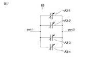
図7は、上記図4乃至図6に示した回路における整合回路48の具体的な構成例を示している。図7において、容量A3−1,…,A3−4はアクチュエータによりデジタル的に(2値的に)容量値を変化させることができるMEMS可変容量である。これら容量A3−1,…,A3−4における一方の電極port1はアンテナに、他方の電極port2は接地点に接続される。 FIG. 7 shows a specific configuration example of the matching
この整合回路48のパターンレイアウトは、例えば図8のようになる。容量A3−j(j=1,2,3,4)は、各々が2j−1Cもしくは0の容量値が実現できるデジタル可変容量である。このように容量値をバイナリ的に割り振ることにより、4個のデジタル可変容量がそれぞれ1C,2C,4C,8Cの4通り、合計で16通りに容量値を変化させることができる。勿論、これは一例であり、デジタル可変容量の数は4以外であっても良い。The pattern layout of the matching
上記図7及び図8に示したデジタル可変容量(容量A3−1,…,A3−4)として、図1乃至図3に示した構成を採用することにより、低電圧・低消費電力の整合回路48が実現できる。また、圧電型と静電型を併用し、それぞれの利点を生かし且つ欠点を補償するハイブリッド型に構成したので、容量部の面積を大きくしても密着性を確保できる。従って、前述したバイナリ可変の構成を採用することができ、整合回路48全体のチップ面積を縮小できる。 As the digital variable capacitors (capacitances A3-1,..., A3-4) shown in FIGS. 7 and 8, the configuration shown in FIGS. 1 to 3 is adopted, thereby matching the low voltage and low power consumption. 48 can be realized. In addition, since the piezoelectric type and the electrostatic type are used in combination, and the hybrid type is configured to take advantage of each and compensate for the defects, the adhesiveness can be ensured even if the area of the capacitor portion is increased. Therefore, the binary variable configuration described above can be adopted, and the entire chip area of the matching
[第2の実施形態]
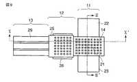
図9及び図10はそれぞれ、この発明の第2の実施形態に係る半導体装置について説明するためのもので、図9は可変容量の平面図、図10は図9のX−X’線に沿った断面図である。図9におけるIII−III’線に沿った断面は、図3と同じになっている。[Second Embodiment]
9 and 10 are each for explaining a semiconductor device according to the second embodiment of the present invention. FIG. 9 is a plan view of a variable capacitor, and FIG. 10 is taken along the line XX 'in FIG. FIG. The cross section along the line III-III ′ in FIG. 9 is the same as FIG.
この半導体装置は、可変容量部11、静電アクチュエータ部12及び圧電アクチュエータ部13を含んで構成されている。これらは基板(例えばシリコン基板)10上にアンカー27で弾性部材15の一端が固定された構造体中に形成される。上記弾性部材15と基板10との間には空隙35’が形成されており、上記圧電アクチュエータ部13と上記静電アクチュエータ部12を駆動することによって上記弾性部材15の他端(可変容量部11の上部電極21)が基板10(可変容量部11の下部電極22)に近づくように変形し、上記弾性部材15と基板10との間の距離が変化するようになっている。 This semiconductor device includes a
図9及び図10において、図1及び図2と同一構成部には同じ符号を付してその詳細な説明は省略する。 9 and 10, the same components as those in FIGS. 1 and 2 are denoted by the same reference numerals, and detailed description thereof is omitted.
すなわち、本第2の実施形態は、弾性部材15を片持ち式にしたものである。このような構成であっても基本的には第1の実施形態と同様な動作を行い、実質的に同じ作用効果が得られる。 That is, in the second embodiment, the
[第3の実施形態]
図11は、この発明の第3の実施形態に係る半導体装置について説明するためのもので、可変容量の平面図である。この半導体装置は、可変容量部11、静電アクチュエータ部12−1,12−2及び圧電アクチュエータ部13−1,13−2,13−3,13−4を含んで構成されている。本第3の実施形態では、可変容量部、静電アクチュエータ部及び圧電アクチュエータ部を直線的に配置するのではなく、圧電アクチュエータ部13−1,13−2,13−3,13−4の配置を変えている。すなわち、圧電アクチュエータ部13−1と13−3は、静電アクチュエータ12−1を挟んで対向する方向に配置され、圧電アクチュエータ部13−2と13−4は、静電アクチュエータ12−2を挟んで対向する方向に配置されている。[Third Embodiment]
FIG. 11 is a plan view of a variable capacitor for explaining a semiconductor device according to the third embodiment of the present invention. This semiconductor device includes a
このような構成であっても基本的には第1の実施形態と同様な動作を行い、同じ作用効果が得られる。しかも、可変容量部、静電アクチュエータ部及び圧電アクチュエータ部を直線的に配置する場合に比べて、弾性部材15の引っ張り応力を緩和してより小さい力で効果的に容量値を変化させることができる。 Even with such a configuration, basically the same operation as that of the first embodiment is performed, and the same effect can be obtained. Moreover, compared with the case where the variable capacitance portion, the electrostatic actuator portion, and the piezoelectric actuator portion are linearly arranged, the tensile stress of the
なお、本第3の実施形態も上述した第2の実施形態と同様に、弾性部材15を片持ち式にしても良い。 In the third embodiment, the
[第4の実施形態]
図12は、この発明の第4の実施形態に係る半導体装置について説明するためのもので、可変容量の平面図である。この半導体装置は、可変容量部11、静電アクチュエータ部12−1,12−2及び圧電アクチュエータ部13−1,13−2,13−3,13−4を含んで構成されている。本第4の実施形態では、圧電アクチュエータ部13−1,13−2,13−3,13−4を折曲した平面パターンで構成している。[Fourth Embodiment]
FIG. 12 is a plan view of a variable capacitor for explaining a semiconductor device according to the fourth embodiment of the present invention. This semiconductor device includes a
このような構成であっても基本的には第1,第3の実施形態と同様な動作を行い、実質的に同じ作用効果が得られる。また、圧電アクチュエータ部13−1,13−2,13−3,13−4の折曲部がバネとして働き、小さい力で効果的に容量値を変化させることができる。 Even with such a configuration, basically the same operation as in the first and third embodiments is performed, and substantially the same operational effects can be obtained. Further, the bent portions of the piezoelectric actuator portions 13-1, 13-2, 13-3, and 13-4 function as springs, and the capacitance value can be effectively changed with a small force.
なお、上述した第2の実施形態と同様に、弾性部材15を片持ち式にしても良いのは勿論である。 Needless to say, the
[第5の実施形態]
図13及び図14はそれぞれ、この発明の第5の実施形態に係る半導体装置について説明するためのもので、図13は可変容量の平面図、図14は図13のXIV−XIV’線に沿った断面図である。図13におけるII−II’線に沿った断面は、図2と実質的に同じ構成になっている。[Fifth Embodiment]
FIGS. 13 and 14 are diagrams for explaining a semiconductor device according to the fifth embodiment of the present invention. FIG. 13 is a plan view of a variable capacitor, and FIG. 14 is taken along the line XIV-XIV ′ in FIG. FIG. The cross section taken along the line II-II ′ in FIG. 13 has substantially the same configuration as FIG.
すなわち、この半導体装置は、可変容量部11の上部電極21がフロートではなく、コンタクト36で固定されている。これによって、上部電極21には上記コンタクト36を介して電位を印加できる。 That is, in this semiconductor device, the
このような構成であっても基本的には第1の実施形態と同様な動作を行い、実質的に同じ作用効果が得られる。また、上部電極21を電気的に固定できるので、可変容量部11の容量を稼ぐことができる。しかも、可変容量部11の下部電極が1つで済むので、パターン占有面積を小さくできる。更に、上部電極21を接地しておけば製造プロセスにおけるチャージアップを防止することもできる。 Even with such a configuration, basically the same operation as in the first embodiment is performed, and substantially the same operational effects can be obtained. Moreover, since the
なお、上述した第2の実施形態と同様に、弾性部材15を片持ち式にしても良いのは勿論である。 Needless to say, the
[第6の実施形態]
図15及び図16はそれぞれ、この発明の第6の実施形態に係る半導体装置について説明するためのもので、図15は可変容量の平面図、図16は図15のXVI−XVI’線に沿った断面図である。図15におけるIII−III’線に沿った断面は、図3と同じになっている。[Sixth Embodiment]
15 and 16 are each for explaining a semiconductor device according to the sixth embodiment of the present invention. FIG. 15 is a plan view of a variable capacitor, and FIG. 16 is along the line XVI-XVI ′ of FIG. FIG. The cross section along the line III-III ′ in FIG. 15 is the same as FIG.
本第6の実施形態では、圧電アクチュエータ部13−1,13−2の圧電膜28−1,28−2、上部電極29−1,29−2及び下部電極30−1,30−2を、静電アクチュエータ部12−1,12−2の下部電極26−1,26−2と対向するように延設している。換言すれば、下部電極30−1,30−2を、静電アクチュエータ部12−1,12−2の上部電極として利用している。 In the sixth embodiment, the piezoelectric films 28-1, 28-2, the upper electrodes 29-1, 29-2 and the lower electrodes 30-1, 30-2 of the piezoelectric actuator units 13-1, 13-2 It extends so as to face the lower electrodes 26-1 and 26-2 of the electrostatic actuator sections 12-1 and 12-2. In other words, the lower electrodes 30-1 and 30-2 are used as upper electrodes of the electrostatic actuator units 12-1 and 12-2.
このような構成であっても基本的には第1の実施形態と同様な動作を行い、実質的に同じ作用効果が得られる。 Even with such a configuration, basically the same operation as in the first embodiment is performed, and substantially the same operational effects can be obtained.
なお、上述した第2の実施形態と同様に、弾性部材15を片持ち式にしても良いのは勿論である。 Needless to say, the
[第7の実施形態]
図17及び図18はそれぞれ、この発明の第7の実施形態に係る半導体装置について説明するためのもので、図17はスイッチの平面図、図18は図17のXVIII−XVIII’線に沿った断面図である。[Seventh Embodiment]
FIGS. 17 and 18 are respectively for explaining a semiconductor device according to the seventh embodiment of the present invention. FIG. 17 is a plan view of the switch, and FIG. 18 is taken along the line XVIII-XVIII ′ of FIG. It is sectional drawing.
この半導体装置は、スイッチ部16、静電アクチュエータ部12−1,12−2及び圧電アクチュエータ部13−1,13−2を含んで構成されている。これらは基板(例えばシリコン基板)10上にアンカー27−1,27−2で弾性部材15の両端が固定された構造体中に形成される。上記弾性部材15と基板10との間には空洞35が形成されており、上記圧電アクチュエータ部13−1,13−2と上記静電アクチュエータ部12−1,12−2とを駆動することによって上記弾性部材15の中央部(スイッチ部16)が基板10に近づくように変形し、スイッチがオン/オフするようになっている。 This semiconductor device includes a
図17及び図18において、図1及び図2と同一構成部には同じ符号を付してその詳細な説明は省略する。 17 and 18, the same components as those in FIGS. 1 and 2 are denoted by the same reference numerals, and detailed description thereof is omitted.
すなわち、図1及び図2における可変容量部11に代えてスイッチ部16を設けたものである。このスイッチ部16は、上部電極21と下部電極22,23を備えている。この上部電極21と下部電極22,23は露出されているので、空気に触れて酸化し、接触抵抗が上昇したり接触不良になったりしないように金かプラチナを用いると良い。上記上部電極21はフロートとなっており、上記静電アクチュエータ部12−1,12−2及び上記圧電アクチュエータ部13−1,13−2で上下方向に可動になっている。上記スイッチ部16の上部電極21がアクチュエータ部12−1,12−2,13−1,13−2により下げられると、この上部電極21の突起部21Aが下部電極22,23と接触して電気的に接続される(スイッチオン)。 That is, a
一方、上部電極21が上がっている状態では、上部電極21と絶縁膜33の間に約1.5μmの隙間ができる(スイッチオフ)。このようにして、上部電極21を上下動することにより、スイッチのオン/オフが実現できる。 On the other hand, when the
なお、前述した第2の実施形態と同様に弾性部材15を片持ち式で構成しても良い。また、第3の実施形態のように静電アクチュエータ部12−1,12−2と圧電アクチュエータ部13−1,13−2,13−3,13−4を配置しても良く、第4の実施形態のように配置しても良い。更に、第5の実施形態と同様に上部電極21をコンタクト36で固定しても良いのは勿論である。 In addition, you may comprise the
次に、第2の実施形態に係る半導体装置である可変容量を例にとって、種々の駆動方法について説明する。 Next, various driving methods will be described by taking a variable capacitor as a semiconductor device according to the second embodiment as an example.
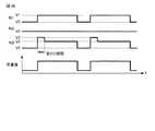
(第1の駆動方法)
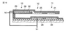
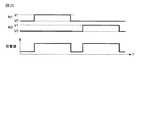
図19は、この発明の第2の実施形態に係る半導体装置の第1の駆動方法について説明するための模式図であり、図20は本駆動方法における各端子の印加電圧と容量値との関係を示している。圧電アクチュエータ部13の上部電極29と静電アクチュエータ部12の下部電極26をショートさせ(端子N1)、圧電アクチュエータ部13の下部電極30(端子N2)に電圧V0を与えると容量値は所定の状態で安定する。可変容量部11の上部電極21を下げる際には、端子N2を電圧V0に保った状態で端子N1の電圧をV0からV1に上げる。電圧V0は例えば0V、電圧V1は例えば3Vとする。(First driving method)
FIG. 19 is a schematic diagram for explaining the first driving method of the semiconductor device according to the second embodiment of the present invention, and FIG. 20 shows the relationship between the applied voltage and capacitance value of each terminal in this driving method. Is shown. When the
これによって、可変容量部11の上部電極21と下部電極22,23の電極間距離が近づいて容量値が増大する。 As a result, the distance between the electrodes of the
なお、図20のタイミングチャートにおける端子N1と端子N2の電圧波形を入れ替えても良い。この場合には、圧電アクチュエータ13が電圧印加により下向きに反るように、圧電膜28の分極の向きや圧電駆動用の上部電極29と下部電極30の膜厚を調整する。 Note that the voltage waveforms at the terminals N1 and N2 in the timing chart of FIG. 20 may be interchanged. In this case, the direction of polarization of the
(第2の駆動方法)
図21は、この発明の第2の実施形態に係る半導体装置の第2の駆動方法について説明するための模式図であり、図22は本駆動方法における各端子の印加電圧と容量値との関係を示している。この駆動例では、電圧V1を印加する端子をN1→N2→N1→N2→…のように交互に変えている。これにより、静電アクチュエータ12の絶縁膜33に加わる電界の向きがスイッチングのたびに変わり、絶縁膜33に電荷がトラップされ難くなる。この結果、スイッチング回数を106回より増やすことが可能となる。(Second driving method)
FIG. 21 is a schematic diagram for explaining a second driving method of the semiconductor device according to the second embodiment of the present invention, and FIG. 22 shows the relationship between the applied voltage and capacitance value of each terminal in this driving method. Is shown. In this driving example, the terminal to which the voltage V1 is applied is alternately changed in the order of N1, N2, N1, N2,. As a result, the direction of the electric field applied to the insulating
なお、ここでは、圧電膜28としてPZTを採用する。PZT膜の膜厚や組成は、電圧V1以下で分極が反転するように決定する。これにより、電界の向きが変わっても圧電アクチュエータ13を常に下方に変位させることができる。 Here, PZT is adopted as the
(第3の駆動方法)
図23は、この発明の第2の実施形態に係る半導体装置の第3の駆動方法について説明するための模式図であり、図24は本駆動方法における各端子の印加電圧と容量値との関係を示している。圧電アクチュエータ13の上部電極29と静電アクチュエータ12の下部電極26を別端子N1,N3とし、図24に示すように電圧印加のタイミングをtdだけずらしている。(Third driving method)
FIG. 23 is a schematic diagram for explaining a third driving method of the semiconductor device according to the second embodiment of the present invention. FIG. 24 shows the relationship between the applied voltage and capacitance value of each terminal in this driving method. Is shown. The
これにより、スイッチング時のピーク電流値を削減でき、電源電圧の低下を抑制できる。上記遅延時間tdは、例えば100nsとする。図24では端子N1の電位の立ち上がりの方が端子N3よりもtdだけ早いが、逆に端子N3の電位の立ち上がりを端子N1より早くしても良い。また、端子N1,N3の印加電圧V1,V2は同じ電圧でも良いし、異なる電圧でも良い。 Thereby, the peak current value at the time of switching can be reduced, and the fall of a power supply voltage can be suppressed. The delay time td is, for example, 100 ns. In FIG. 24, the rising of the potential at the terminal N1 is earlier than the terminal N3 by td, but conversely, the rising of the potential at the terminal N3 may be earlier than that of the terminal N1. The applied voltages V1 and V2 at the terminals N1 and N3 may be the same voltage or different voltages.
(第4の駆動方法)
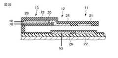
図25は、この発明の第2の実施形態に係る半導体装置の第4の駆動方法について説明するための模式図であり、図26は本駆動方法における各端子の印加電圧と容量値との関係を示している。この駆動例では、端子N3に電圧を印加する際に、立ち上がりの第1の期間だけV2より大きな電圧V3を印加するようにしている。これにより、第1の期間内だけ電極間の静電引力が増加し、電極間の密着性を向上させることができる。電極同士が一度密着すると、極板間距離が短く静電引力が強い状態になっているため、より低い電圧(V2)でも密着状態を保持できる。具体的には、電圧V2は例えば3V、電圧V3は例えば5V、第1の期間は例えば1μsである。(Fourth driving method)
FIG. 25 is a schematic diagram for explaining a fourth driving method of the semiconductor device according to the second embodiment of the present invention. FIG. 26 shows the relationship between the applied voltage and capacitance value of each terminal in this driving method. Is shown. In this driving example, when a voltage is applied to the terminal N3, a voltage V3 larger than V2 is applied only during the first rising period. Thereby, the electrostatic attraction between the electrodes increases only within the first period, and the adhesion between the electrodes can be improved. Once the electrodes are in close contact with each other, the distance between the electrodes is short and the electrostatic attractive force is strong, so that the close contact state can be maintained even at a lower voltage (V2). Specifically, the voltage V2 is 3 V, for example, the voltage V3 is 5 V, for example, and the first period is 1 μs, for example.
(第5の駆動方法)
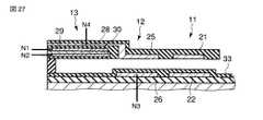
図27は、この発明の第2の実施形態に係る半導体装置の第5の駆動方法について説明するための模式図であり、図28は本駆動方法における各端子の印加電圧と容量値との関係を示している。この駆動例では、圧電アクチュエータ13の駆動電極と静電アクチュエータ12の駆動電極を完全に分離している。そして、各端子N1,N2,N3,N4に図28に示すような駆動電圧を与える。(Fifth driving method)
FIG. 27 is a schematic diagram for explaining a fifth driving method of the semiconductor device according to the second embodiment of the present invention. FIG. 28 shows the relationship between the applied voltage and capacitance value of each terminal in this driving method. Is shown. In this drive example, the drive electrode of the
これにより、静電アクチュエータ12の絶縁膜33に対しては、第2の駆動方法と同様な効果を期待できる。また、静電アクチュエータ12の上部電極25が圧電アクチュエータ13の電極29,30と分離されているため、圧電膜28として分極反転特性のないAlNを採用することが可能となる。 Thereby, the same effect as the second driving method can be expected for the insulating
AlNは、PZTを採用した場合よりも分極反転による疲労が少なくなるため、スイッチング回数をより増やすことが可能となる。 Since AlN has less fatigue due to polarization reversal than when PZT is employed, the number of switching operations can be increased.
なお、上述した第1乃至第5の駆動方法のいくつかを組み合わせた駆動方法を採用しても良い。また、第2の実施形態の駆動方法を例にとり説明したが、他の全ての実施形態の可変容量やスイッチにも同様にして適用できるのは勿論である。 Note that a driving method in which some of the first to fifth driving methods described above are combined may be employed. Further, the driving method of the second embodiment has been described as an example, but it is needless to say that the driving method can be similarly applied to the variable capacitors and switches of all other embodiments.
また、この発明の実施形態に係る可変容量は、アンテナ整合回路以外の回路、例えばVCOにも使用可能である。図29は、MEMS可変容量を搭載したVCO回路を示す回路図である。この回路は、インダクタL1,L2、トランジスタTr1,Tr2、定電流源Iv及びMEMS可変容量Cvを備え、MEMS可変容量Cvの容量値を変化させることにより発振周波数が変化するようになっている。 Further, the variable capacitor according to the embodiment of the present invention can be used for a circuit other than the antenna matching circuit, for example, a VCO. FIG. 29 is a circuit diagram showing a VCO circuit equipped with a MEMS variable capacitor. This circuit includes inductors L1 and L2, transistors Tr1 and Tr2, a constant current source Iv, and a MEMS variable capacitor Cv, and the oscillation frequency is changed by changing the capacitance value of the MEMS variable capacitor Cv.
図30は、この発明の実施形態に係るスイッチをマルチバンド携帯電話向けMEMSスイッチに用いる場合の構成例を示す回路図である。図30に示すマルチバンド携帯電話は、n個の出力システムRxとn個の入力システムTxを、MEMSスイッチSP2nTで切り替えるようになっている。各出力システムRxの入力段と各入力システムTxの出力段にはフィルタFI1〜FIn,FO1〜FOnが設けられている。 FIG. 30 is a circuit diagram showing a configuration example when the switch according to the embodiment of the present invention is used in a MEMS switch for a multiband mobile phone. The multiband mobile phone shown in FIG. 30 is configured to switch between n output systems Rx and n input systems Tx with a MEMS switch SP2nT. Filters FI1 to FIn and FO1 to FOn are provided at the input stage of each output system Rx and the output stage of each input system Tx.
以上第1乃至第7の実施形態と第1乃至第5の駆動方法を用いてこの発明の説明を行ったが、この発明は上記各実施形態や駆動方法に限定されるものではなく、実施段階ではその要旨を逸脱しない範囲で種々に変形することが可能である。また、上記各実施形態には種々の段階の発明が含まれており、開示される複数の構成要件の適宜な組み合わせにより種々の発明が抽出され得る。例えば各実施形態に示される全構成要件からいくつかの構成要件が削除されても、発明が解決しようとする課題の欄で述べた課題の少なくとも1つが解決でき、発明の効果の欄で述べられている効果の少なくとも1つが得られる場合には、この構成要件が削除された構成が発明として抽出され得る。 Although the present invention has been described above using the first to seventh embodiments and the first to fifth driving methods, the present invention is not limited to the above-described embodiments and driving methods, and the implementation stage Then, various modifications can be made without departing from the scope of the invention. Each of the above embodiments includes inventions at various stages, and various inventions can be extracted by appropriately combining a plurality of disclosed constituent elements. For example, even if some constituent elements are deleted from all the constituent elements shown in each embodiment, at least one of the problems described in the column of the problem to be solved by the invention can be solved, and is described in the column of the effect of the invention. When at least one of the effects is obtained, a configuration in which this configuration requirement is deleted can be extracted as an invention.
10…基板(シリコン基板)、11…可変容量部、12,12−1,12−2…静電アクチュエータ部、13,13−1,13−2,13−3,13−4…圧電アクチュエータ部、14…窓、15…弾性部材、16…スイッチ部、21…上部電極、22,23…下部電極、25−1,25−2…上部電極、26−1,26−2…下部電極、27−1,27−2…アンカー、28−1,28−2…圧電膜、29−1,29−2…上部電極、30−1,30−2…下部電極、31,32,33,34…絶縁膜、35…空洞、35’…空隙、36…コンタクト。 DESCRIPTION OF
Claims (5)
Translated fromJapanese前記弾性部材の他端に配置された第1の電極と、
前記第1の電極と対向するように前記基板上に配置された第2の電極と、
前記弾性部材内に配置され、前記弾性部材の他端を前記基板に近づけるように変形させる圧電アクチュエータと、
前記弾性部材内に配置された第3の電極と、前記第3の電極と対向するように前記基板上に配置された第4の電極とからなり、前記弾性部材の他端を前記基板に近づけるように変形させる静電アクチュエータと
を具備し、前記圧電アクチュエータと前記静電アクチュエータの駆動によって第1の電極と第2の電極との距離が変化することを特徴とする半導体装置。One end is fixed via an anchor so as to form a gap between the substrate and an elastic member that changes the distance between the other end and the substrate by being deformed,
A first electrode disposed at the other end of the elastic member;
A second electrode disposed on the substrate to face the first electrode;
A piezoelectric actuator disposed in the elastic member and deformed so that the other end of the elastic member approaches the substrate;
It consists of the 3rd electrode arrange | positioned in the said elastic member, and the 4th electrode arrange | positioned on the said board | substrate so that the said 3rd electrode may be opposed, The other end of the said elastic member is brought close to the said board | substrate. A semiconductor device, wherein the distance between the first electrode and the second electrode is changed by driving the piezoelectric actuator and the electrostatic actuator.
Priority Applications (3)
| Application Number | Priority Date | Filing Date | Title |
|---|---|---|---|
| JP2005113483AJP2006294866A (en) | 2005-04-11 | 2005-04-11 | Semiconductor device |
| US11/280,385US20060226735A1 (en) | 2005-04-11 | 2005-11-17 | Semiconductor device formed by using MEMS technique |
| CNA2006100747161ACN1848342A (en) | 2005-04-11 | 2006-04-11 | Semiconductor devices fabricated using MEMS technology |
Applications Claiming Priority (1)
| Application Number | Priority Date | Filing Date | Title |
|---|---|---|---|
| JP2005113483AJP2006294866A (en) | 2005-04-11 | 2005-04-11 | Semiconductor device |
Publications (1)
| Publication Number | Publication Date |
|---|---|
| JP2006294866Atrue JP2006294866A (en) | 2006-10-26 |
Family
ID=37077849
Family Applications (1)
| Application Number | Title | Priority Date | Filing Date |
|---|---|---|---|
| JP2005113483AAbandonedJP2006294866A (en) | 2005-04-11 | 2005-04-11 | Semiconductor device |
Country Status (3)
| Country | Link |
|---|---|
| US (1) | US20060226735A1 (en) |
| JP (1) | JP2006294866A (en) |
| CN (1) | CN1848342A (en) |
Cited By (8)
| Publication number | Priority date | Publication date | Assignee | Title |
|---|---|---|---|---|
| JP2007075931A (en)* | 2005-09-13 | 2007-03-29 | Toshiba Corp | Semiconductor device and manufacturing method thereof |
| JP2009118627A (en)* | 2007-11-06 | 2009-05-28 | Toshiba Corp | Actuator |
| JP2009170677A (en)* | 2008-01-16 | 2009-07-30 | Advantest Corp | Piezoelectric drive device, piezoelectric drive control method, and electronic device |
| US7633213B2 (en)* | 2005-03-15 | 2009-12-15 | Panasonic Corporation | Actuator, switch using the actuator, and method of controlling the actuator |
| WO2011158708A1 (en)* | 2010-06-17 | 2011-12-22 | 株式会社村田製作所 | Variable capacitance device |
| WO2012099084A1 (en)* | 2011-01-19 | 2012-07-26 | 株式会社村田製作所 | Mems module, variable reactance circuit and antenna device |
| JP2020035828A (en)* | 2018-08-28 | 2020-03-05 | 株式会社東芝 | Ic chip and method of determining fuse to be cut off |
| WO2022153696A1 (en)* | 2021-01-12 | 2022-07-21 | ローム株式会社 | Mems switch |
Families Citing this family (19)
| Publication number | Priority date | Publication date | Assignee | Title |
|---|---|---|---|---|
| WO2006123788A1 (en)* | 2005-05-19 | 2006-11-23 | Rohm Co., Ltd. | Mems element, mems device and mems element manufacturing method |
| JP2008103571A (en)* | 2006-10-19 | 2008-05-01 | Toshiba Corp | Semiconductor device and manufacturing method thereof |
| JP2008238330A (en)* | 2007-03-27 | 2008-10-09 | Toshiba Corp | MEMS device and portable communication terminal having the MEMS device |
| JP4334581B2 (en)* | 2007-04-27 | 2009-09-30 | 株式会社東芝 | Electrostatic actuator |
| US7956429B1 (en)* | 2007-08-02 | 2011-06-07 | Rf Micro Devices, Inc. | Insulator layer based MEMS devices |
| JP5363005B2 (en)* | 2008-02-20 | 2013-12-11 | 富士通株式会社 | Variable capacitance element, matching circuit element, and portable terminal device |
| JP5081038B2 (en)* | 2008-03-31 | 2012-11-21 | パナソニック株式会社 | MEMS switch and manufacturing method thereof |
| DE102009045428B4 (en)* | 2009-10-07 | 2019-06-19 | Robert Bosch Gmbh | Manufacturing method for a micromechanical component and micromechanical component |
| US8552621B2 (en)* | 2009-11-30 | 2013-10-08 | The Trustees Of The University Of Pennsylvania | Systems and methods for operating piezoelectric switches |
| CN103843100B (en)* | 2011-10-06 | 2016-04-27 | 富士通株式会社 | Mems switch |
| KR101272983B1 (en)* | 2011-12-20 | 2013-06-11 | 엘지이노텍 주식회사 | Capacitor |
| US9096422B2 (en)* | 2013-02-15 | 2015-08-04 | Fujifilm Dimatix, Inc. | Piezoelectric array employing integrated MEMS switches |
| US9362620B1 (en)* | 2013-05-20 | 2016-06-07 | Amazon Technologies, Inc. | Dynamically reconfiguring antenna bandwidth based on user scenario |
| CN103545108B (en)* | 2013-10-29 | 2016-01-20 | 苏州科技学院 | MEMS variable capacitor that a kind of thermic drives and preparation method thereof |
| JP2015173207A (en)* | 2014-03-12 | 2015-10-01 | 株式会社東芝 | MEMS equipment |
| CN103943417A (en)* | 2014-04-09 | 2014-07-23 | 苏州锟恩电子科技有限公司 | Capacitive RF MEMS switch |
| CN103943418A (en)* | 2014-04-14 | 2014-07-23 | 苏州锟恩电子科技有限公司 | Elastic micro-bridge type RF MEMS switch |
| CN108288567B (en)* | 2018-03-09 | 2019-07-09 | 清华大学 | relay |
| CN118632177A (en)* | 2024-07-03 | 2024-09-10 | 西安电子科技大学 | Capacitive MEMS microphone based on charge control structure |
Family Cites Families (4)
| Publication number | Priority date | Publication date | Assignee | Title |
|---|---|---|---|---|
| US6355534B1 (en)* | 2000-01-26 | 2002-03-12 | Intel Corporation | Variable tunable range MEMS capacitor |
| US6504118B2 (en)* | 2000-10-27 | 2003-01-07 | Daniel J Hyman | Microfabricated double-throw relay with multimorph actuator and electrostatic latch mechanism |
| US7098577B2 (en)* | 2002-10-21 | 2006-08-29 | Hrl Laboratories, Llc | Piezoelectric switch for tunable electronic components |
| ITTO20030238A1 (en)* | 2003-03-28 | 2004-09-29 | Tetra Laval Holdings & Finance | USABLE INDUCTION WELDING DEVICE AND METHOD |
- 2005
- 2005-04-11JPJP2005113483Apatent/JP2006294866A/ennot_activeAbandoned
- 2005-11-17USUS11/280,385patent/US20060226735A1/ennot_activeAbandoned
- 2006
- 2006-04-11CNCNA2006100747161Apatent/CN1848342A/enactivePending
Cited By (9)
| Publication number | Priority date | Publication date | Assignee | Title |
|---|---|---|---|---|
| US7633213B2 (en)* | 2005-03-15 | 2009-12-15 | Panasonic Corporation | Actuator, switch using the actuator, and method of controlling the actuator |
| JP2007075931A (en)* | 2005-09-13 | 2007-03-29 | Toshiba Corp | Semiconductor device and manufacturing method thereof |
| JP2009118627A (en)* | 2007-11-06 | 2009-05-28 | Toshiba Corp | Actuator |
| JP2009170677A (en)* | 2008-01-16 | 2009-07-30 | Advantest Corp | Piezoelectric drive device, piezoelectric drive control method, and electronic device |
| WO2011158708A1 (en)* | 2010-06-17 | 2011-12-22 | 株式会社村田製作所 | Variable capacitance device |
| WO2012099084A1 (en)* | 2011-01-19 | 2012-07-26 | 株式会社村田製作所 | Mems module, variable reactance circuit and antenna device |
| US9350073B2 (en) | 2011-01-19 | 2016-05-24 | Murata Manufacturing Co., Ltd. | MEMS module, variable reactance circuit and antenna device |
| JP2020035828A (en)* | 2018-08-28 | 2020-03-05 | 株式会社東芝 | Ic chip and method of determining fuse to be cut off |
| WO2022153696A1 (en)* | 2021-01-12 | 2022-07-21 | ローム株式会社 | Mems switch |
Also Published As
| Publication number | Publication date |
|---|---|
| US20060226735A1 (en) | 2006-10-12 |
| CN1848342A (en) | 2006-10-18 |
Similar Documents
| Publication | Publication Date | Title |
|---|---|---|
| JP2006294866A (en) | Semiconductor device | |
| US7027282B2 (en) | Method and arrangement for controlling micromechanical element | |
| JP5204066B2 (en) | MEMS device | |
| US8928435B2 (en) | Electromechanical switch device and method of operating the same | |
| JP5537180B2 (en) | Electrostatic actuator device | |
| US9431201B2 (en) | Micromechanical resonant switches and charge pumps | |
| US8363381B2 (en) | Variable capacitive element, variable capacitive device, and method for driving the variable capacitive element | |
| US20100237929A1 (en) | Voltage generating circuit for electrostatic mems actuator | |
| US7602261B2 (en) | Micro-electromechanical system (MEMS) switch | |
| US7109641B2 (en) | Low voltage micro switch | |
| US8183946B2 (en) | Charge biased MEM resonator | |
| Lin et al. | A micromechanical resonant charge pump | |
| JP2008258670A (en) | Antenna device and portable terminal | |
| JP4707424B2 (en) | Variable capacitance element, variable capacitance device, and mobile phone using variable capacitance device | |
| JP4867007B2 (en) | MEMS switch and portable wireless terminal device | |
| CN111934635B (en) | Micro-electromechanical wireless signal wake-up receiver and preparation method thereof | |
| KR20060078097A (en) | Piezoelectric and Constant Power Driving RF MEMS Switches | |
| KR100323715B1 (en) | micro switch and method for fabricating the same | |
| US9496110B2 (en) | Micro-electro-mechanical system (MEMS) structure and design structures | |
| KR100364726B1 (en) | micro switch and method for fabricating the same | |
| JP2006331742A (en) | Electromechanical switch | |
| US7300813B2 (en) | Method for manufacturing micro-machined switch using pull-up type contact pad | |
| KR101292928B1 (en) | RF MEMS switch | |
| KR100520891B1 (en) | RF MEMS switch using residual stress and piezo-driving force | |
| KR100650272B1 (en) | Piezoelectric RF MEMS Switch and Multi-Band Antenna Module Using the Same |
Legal Events
| Date | Code | Title | Description |
|---|---|---|---|
| A621 | Written request for application examination | Free format text:JAPANESE INTERMEDIATE CODE: A621 Effective date:20080219 | |
| A762 | Written abandonment of application | Free format text:JAPANESE INTERMEDIATE CODE: A762 Effective date:20090202 |