JP2006293312A - Electrophoretic display device - Google Patents
Electrophoretic display deviceDownload PDFInfo
- Publication number
- JP2006293312A JP2006293312AJP2006020013AJP2006020013AJP2006293312AJP 2006293312 AJP2006293312 AJP 2006293312AJP 2006020013 AJP2006020013 AJP 2006020013AJP 2006020013 AJP2006020013 AJP 2006020013AJP 2006293312 AJP2006293312 AJP 2006293312A
- Authority
- JP
- Japan
- Prior art keywords
- electrode
- display device
- electrophoretic display
- substrate
- region
- Prior art date
- Legal status (The legal status is an assumption and is not a legal conclusion. Google has not performed a legal analysis and makes no representation as to the accuracy of the status listed.)
- Pending
Links
Images


Classifications
- G—PHYSICS
- G02—OPTICS
- G02F—OPTICAL DEVICES OR ARRANGEMENTS FOR THE CONTROL OF LIGHT BY MODIFICATION OF THE OPTICAL PROPERTIES OF THE MEDIA OF THE ELEMENTS INVOLVED THEREIN; NON-LINEAR OPTICS; FREQUENCY-CHANGING OF LIGHT; OPTICAL LOGIC ELEMENTS; OPTICAL ANALOGUE/DIGITAL CONVERTERS
- G02F1/00—Devices or arrangements for the control of the intensity, colour, phase, polarisation or direction of light arriving from an independent light source, e.g. switching, gating or modulating; Non-linear optics
- G02F1/01—Devices or arrangements for the control of the intensity, colour, phase, polarisation or direction of light arriving from an independent light source, e.g. switching, gating or modulating; Non-linear optics for the control of the intensity, phase, polarisation or colour
- G02F1/165—Devices or arrangements for the control of the intensity, colour, phase, polarisation or direction of light arriving from an independent light source, e.g. switching, gating or modulating; Non-linear optics for the control of the intensity, phase, polarisation or colour based on translational movement of particles in a fluid under the influence of an applied field
- G02F1/166—Devices or arrangements for the control of the intensity, colour, phase, polarisation or direction of light arriving from an independent light source, e.g. switching, gating or modulating; Non-linear optics for the control of the intensity, phase, polarisation or colour based on translational movement of particles in a fluid under the influence of an applied field characterised by the electro-optical or magneto-optical effect
- G02F1/167—Devices or arrangements for the control of the intensity, colour, phase, polarisation or direction of light arriving from an independent light source, e.g. switching, gating or modulating; Non-linear optics for the control of the intensity, phase, polarisation or colour based on translational movement of particles in a fluid under the influence of an applied field characterised by the electro-optical or magneto-optical effect by electrophoresis
- G—PHYSICS
- G02—OPTICS
- G02F—OPTICAL DEVICES OR ARRANGEMENTS FOR THE CONTROL OF LIGHT BY MODIFICATION OF THE OPTICAL PROPERTIES OF THE MEDIA OF THE ELEMENTS INVOLVED THEREIN; NON-LINEAR OPTICS; FREQUENCY-CHANGING OF LIGHT; OPTICAL LOGIC ELEMENTS; OPTICAL ANALOGUE/DIGITAL CONVERTERS
- G02F1/00—Devices or arrangements for the control of the intensity, colour, phase, polarisation or direction of light arriving from an independent light source, e.g. switching, gating or modulating; Non-linear optics
- G02F1/01—Devices or arrangements for the control of the intensity, colour, phase, polarisation or direction of light arriving from an independent light source, e.g. switching, gating or modulating; Non-linear optics for the control of the intensity, phase, polarisation or colour
- G02F1/13—Devices or arrangements for the control of the intensity, colour, phase, polarisation or direction of light arriving from an independent light source, e.g. switching, gating or modulating; Non-linear optics for the control of the intensity, phase, polarisation or colour based on liquid crystals, e.g. single liquid crystal display cells
- G02F1/133—Constructional arrangements; Operation of liquid crystal cells; Circuit arrangements
- G02F1/1333—Constructional arrangements; Manufacturing methods
- G02F1/133377—Cells with plural compartments or having plurality of liquid crystal microcells partitioned by walls, e.g. one microcell per pixel
- G—PHYSICS
- G02—OPTICS
- G02F—OPTICAL DEVICES OR ARRANGEMENTS FOR THE CONTROL OF LIGHT BY MODIFICATION OF THE OPTICAL PROPERTIES OF THE MEDIA OF THE ELEMENTS INVOLVED THEREIN; NON-LINEAR OPTICS; FREQUENCY-CHANGING OF LIGHT; OPTICAL LOGIC ELEMENTS; OPTICAL ANALOGUE/DIGITAL CONVERTERS
- G02F1/00—Devices or arrangements for the control of the intensity, colour, phase, polarisation or direction of light arriving from an independent light source, e.g. switching, gating or modulating; Non-linear optics
- G02F1/01—Devices or arrangements for the control of the intensity, colour, phase, polarisation or direction of light arriving from an independent light source, e.g. switching, gating or modulating; Non-linear optics for the control of the intensity, phase, polarisation or colour
- G02F1/165—Devices or arrangements for the control of the intensity, colour, phase, polarisation or direction of light arriving from an independent light source, e.g. switching, gating or modulating; Non-linear optics for the control of the intensity, phase, polarisation or colour based on translational movement of particles in a fluid under the influence of an applied field
- G02F1/1675—Constructional details
- G02F1/1679—Gaskets; Spacers; Sealing of cells; Filling or closing of cells
- G02F1/1681—Gaskets; Spacers; Sealing of cells; Filling or closing of cells having two or more microcells partitioned by walls, e.g. of microcup type
- G—PHYSICS
- G02—OPTICS
- G02F—OPTICAL DEVICES OR ARRANGEMENTS FOR THE CONTROL OF LIGHT BY MODIFICATION OF THE OPTICAL PROPERTIES OF THE MEDIA OF THE ELEMENTS INVOLVED THEREIN; NON-LINEAR OPTICS; FREQUENCY-CHANGING OF LIGHT; OPTICAL LOGIC ELEMENTS; OPTICAL ANALOGUE/DIGITAL CONVERTERS
- G02F1/00—Devices or arrangements for the control of the intensity, colour, phase, polarisation or direction of light arriving from an independent light source, e.g. switching, gating or modulating; Non-linear optics
- G02F1/01—Devices or arrangements for the control of the intensity, colour, phase, polarisation or direction of light arriving from an independent light source, e.g. switching, gating or modulating; Non-linear optics for the control of the intensity, phase, polarisation or colour
- G02F1/165—Devices or arrangements for the control of the intensity, colour, phase, polarisation or direction of light arriving from an independent light source, e.g. switching, gating or modulating; Non-linear optics for the control of the intensity, phase, polarisation or colour based on translational movement of particles in a fluid under the influence of an applied field
- G02F1/1675—Constructional details
- G02F2001/1678—Constructional details characterised by the composition or particle type
Landscapes
- Physics & Mathematics (AREA)
- Nonlinear Science (AREA)
- General Physics & Mathematics (AREA)
- Optics & Photonics (AREA)
- Health & Medical Sciences (AREA)
- Life Sciences & Earth Sciences (AREA)
- Chemical & Material Sciences (AREA)
- Chemical Kinetics & Catalysis (AREA)
- Electrochemistry (AREA)
- Molecular Biology (AREA)
- Electrochromic Elements, Electrophoresis, Or Variable Reflection Or Absorption Elements (AREA)
Abstract
Translated fromJapaneseDescription
Translated fromJapanese本発明は、電気泳動表示装置に関し、特に、別途のカラーフィルタなしで全ての色を実現することができる電気泳動表示装置に関する。 The present invention relates to an electrophoretic display device, and more particularly to an electrophoretic display device that can realize all colors without a separate color filter.
電気泳動表示装置(electrophoric display)は、対向する2つの電極の間に形成される電位差によって2つの電極の間に位置した帯電粒子(charged particles)が反対極性の電極に移動する電気泳動(electrophoresis)現象を利用して文字などの画像を表示する平板表示装置である。
このような電気泳動表示装置は、反射率とコントラスト比が高く、紙のように安定した感じの画像を表示できるメリットがある。さらに、液晶表示装置とは異なって、偏光板、配向膜及び液晶などが不要と言う利点もある。An electrophoretic display is an electrophoresis in which charged particles positioned between two electrodes move to electrodes of opposite polarity due to a potential difference formed between the two electrodes facing each other. This is a flat panel display device that displays an image such as a character using a phenomenon.
Such an electrophoretic display device has a high reflectance and contrast ratio, and has an advantage of being able to display an image with a stable feeling like paper. Further, unlike a liquid crystal display device, there is an advantage that a polarizing plate, an alignment film, a liquid crystal, and the like are unnecessary.
しかし、電気泳動表示装置は、白色及び黒色粒子を所定の形態の微小カプセル(microcapsule)内に分散させる複雑な工程が要求され、製造工程及び生産コストの面で不利であり、フルカラーを実現するためには別途のカラーフィルタを備える必要がある。
本発明は、前記問題点を解決するためのものであって、製造工程を単純化しつつ、フルカラーを実現することができる電気泳動表示装置を提供する。However, the electrophoretic display device requires a complicated process of dispersing white and black particles in a microcapsule having a predetermined shape, which is disadvantageous in terms of manufacturing process and production cost, and realizes full color. Need to be provided with a separate color filter.
The present invention is for solving the above-described problems, and provides an electrophoretic display device capable of realizing full color while simplifying the manufacturing process.
本発明による電気泳動表示装置は、第1基板上に形成されている第1電極と、前記第1基板に対向する第2基板上に形成されている第2電極と、前記第1電極と前記第2電極との間を複数の領域に分離する隔壁と、前記各領域内に含まれ、赤色、緑色及び青色のいずれか一色で着色された複数の帯電粒子を備える。
ここで、隣接する前記各領域には、赤色、緑色及び青色のいずれか一色で着色された複数の帯電粒子が各々含まれている構成とすることができる。The electrophoretic display device according to the present invention includes a first electrode formed on a first substrate, a second electrode formed on a second substrate facing the first substrate, the first electrode, A partition that separates the second electrode into a plurality of regions, and a plurality of charged particles that are included in each region and are colored in any one color of red, green, and blue.
Here, each of the adjacent regions may include a plurality of charged particles colored in any one color of red, green, and blue.
また、前記各領域は、複数の黒色帯電粒子をさらに含む構成とすることができる。
さらに、前記黒色帯電粒子は、前記赤色、緑色及び青色のいずれか一色で着色された複数の帯電粒子と反対電荷を有する構成とすることができる。
また、前記第1電極が前記各領域毎に分離されており、各領域毎に別途の電圧が印加されるように構成できる。Each region may further include a plurality of black charged particles.
Furthermore, the black charged particles may be configured to have a charge opposite to that of the plurality of charged particles colored with any one color of red, green, and blue.
The first electrode may be separated for each region, and a separate voltage may be applied to each region.
前記第1基板上には、互いに交差するゲート線及びデータ線、半導体を備え、前記ゲート線及び前記データ線と電気的に接続されている薄膜トランジスタが形成されている構成とすることができる。
さらに、前記薄膜トランジスタと前記第1電極との間には、有機物質からなる保護膜をさらに有する構成とすることができる。A thin film transistor that includes gate lines, data lines, and semiconductors that cross each other and is electrically connected to the gate lines and the data lines may be formed on the first substrate.
Further, a protective film made of an organic material may be further provided between the thin film transistor and the first electrode.
また、前記データ線上に前記隔壁が形成されているように構成できる。
前記第2電極は、前記各領域毎に中心部が凹んだ形態を有する構成とすることができる。
さらに、前記第2基板と前記第2電極との間に層間膜をさらに有する構成とすることができる。Further, the partition may be formed on the data line.
The second electrode may have a configuration in which a central portion is recessed for each region.
Furthermore, an interlayer film may be further provided between the second substrate and the second electrode.
前記層間膜は、前記各領域毎に中心部が凹んだ形態を有する構成とすることができる。
本発明に係る電気泳動表示装置は、第1基板上に形成されている第1電極と、前記第1基板に対向する第2基板上に形成され凹部を有する第2電極と、前記第1電極と前記第2電極との間を複数の領域に分離する隔壁と、前記各領域内に含まれ、流体内に分散している複数の着色帯電粒子とを備える。The interlayer film may have a configuration in which a central portion is recessed for each region.
The electrophoretic display device according to the present invention includes a first electrode formed on a first substrate, a second electrode formed on a second substrate facing the first substrate and having a recess, and the first electrode. And the second electrode are separated into a plurality of regions, and a plurality of colored charged particles contained in each region and dispersed in the fluid.
ここで、前記凹部は、前記各領域毎に形成されている構成とすることができる。
また、前記第2基板と前記第2電極との間に形成され、凹凸を有する層間膜をさらに有し、前記第2電極の凹部は、前記層間膜の凹凸によって形成される構成とすることができる。
さらに、前記第1基板上に互いに交差するゲート線及びデータ線と半導体を備え、前記ゲート線及び前記データ線と電気的に接続されている薄膜トランジスタが形成されている構成とすることができる。Here, the said recessed part can be set as the structure currently formed for every said area | region.
In addition, an interlayer film having unevenness formed between the second substrate and the second electrode may be further provided, and the recess of the second electrode may be formed by the unevenness of the interlayer film. it can.
In addition, a thin film transistor that includes a gate line, a data line, and a semiconductor that intersect with each other and is electrically connected to the gate line and the data line may be formed on the first substrate.
隔壁によって分離された領域でそれぞれの着色粒子を含むことによって、追加工程が不要で、かつ別途のカラーフィルタなしで多様な色を表現することができ、一側の電極に凹部を有することによってより改善された広視野角特性を実現することができる。 By including each colored particle in the region separated by the partition wall, no additional process is required, and various colors can be expressed without a separate color filter. Improved wide viewing angle characteristics can be realized.
以下、添付した図面を参照して、本発明の実施形態を、本発明が属する技術分野における通常の知識を有する者が容易に実施することができるように詳細に説明する。しかし、本発明は、多様な形態で実現することができ、ここで説明する実施形態に限定されない。
図面は、各種層及び領域を明確に表現するために、厚さを拡大して示している。明細書全体を通じて類似した部分については同一の参照符号を付けている。層、膜、領域、板などの部分が、他の部分の“上に”あるとする時、これは他の部分の“すぐ上に”ある場合に限らず、その中間に更に他の部分がある場合も含む。逆に、ある部分が他の部分の“すぐ上に”あるとする時、これは中間に他の部分がない場合を意味する。Hereinafter, embodiments of the present invention will be described in detail with reference to the accompanying drawings so that a person having ordinary knowledge in the technical field to which the present invention belongs can easily carry out the embodiments. However, the present invention can be realized in various forms and is not limited to the embodiments described herein.
In the drawings, the thickness is enlarged to clearly show various layers and regions. Similar parts are denoted by the same reference numerals throughout the specification. When a layer, film, region, plate, or other part is “on top” of another part, this is not limited to “immediately above” another part, and another part is in the middle. Including some cases. Conversely, when a part is “just above” another part, this means that there is no other part in the middle.
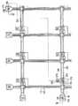
まず、図1を参照して本発明の一実施形態による電気泳動表示装置の駆動原理について説明する。
図1は、本発明の一実施形態による電気泳動表示装置の駆動原理を概略的に示した模式図である。
図1のように、本発明の一実施形態による電気泳動表示装置は、プラス(+)及びマイナス(−)電界を形成するための下部電極190及び上部電極270と、下部電極190と上部電極270との間の領域を分離するための複数の隔壁360を備える。隔壁360によって分離された複数の領域には、絶縁性流体(fluid)310と、絶縁性流体310に分散され、陽性(positive)または陰性(negative)で帯電された複数の赤色粒子300a、緑色粒子300b及び青色粒子300c(以下、着色粒子と言う)が順に充填されている。First, the driving principle of an electrophoretic display device according to an embodiment of the present invention will be described with reference to FIG.
FIG. 1 is a schematic diagram schematically illustrating a driving principle of an electrophoretic display device according to an embodiment of the present invention.
As shown in FIG. 1, the electrophoretic display device according to an embodiment of the present invention includes a
本実施形態による電気泳動表示装置は、対向する下部電極190と上部電極270に電圧を印加して電極両端に電位差(+/−)を形成する場合、陽性または陰性で帯電されている着色粒子300a、300b、300cが電気泳動現象によって反対極性の電極に移動する。この時、着色粒子300a、300b、300cが観察者側の電極に移動する場合、観察者は、着色粒子300a、300b、300cに反射された光によって、赤色、緑色、青色またはこれらの混合色で表現された画像を見ることができる。 In the electrophoretic display device according to the present embodiment, when a voltage is applied to the opposing
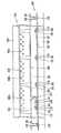
以下、図2及び図3を参照して、本発明の一実施形態による電気泳動表示装置についてより詳細に説明する。
図2は、本発明の一実施形態による薄膜トランジスタ表示板を備える電気泳動表示装置の構造を示した配置図であり、図3は、図2の電気泳動表示装置のIII-III'線に沿った断面図である。Hereinafter, an electrophoretic display device according to an exemplary embodiment of the present invention will be described in more detail with reference to FIGS. 2 and 3.
FIG. 2 is a layout view illustrating a structure of an electrophoretic display device including a thin film transistor array panel according to an embodiment of the present invention, and FIG. 3 is taken along line III-III ′ of the electrophoretic display device of FIG. It is sectional drawing.
本発明の一実施形態による電気泳動表示装置は、薄膜トランジスタ表示板100、対向表示板200、及びこれらの間で隔壁360によって分離される複数の領域に充填され、着色粒子300a、300b、300cを有する絶縁性流体310を備える。
まず、薄膜トランジスタ表示板100には、透明ガラスなどからなる下部基板110上にゲート電極124を有する複数のゲート線121が形成されている。The electrophoretic display device according to an exemplary embodiment of the present invention includes a thin film
First, in the thin film
ゲート線121は、ゲート信号を伝達し、主に図2横方向に延設されている。各ゲート線121の一部は、複数のゲート電極124をなし、他の層または外部駆動回路と接続するための面積が広い端部129を有する。
ゲート線121は、アルミニウムやアルミニウム合金(Al−alloy)などのアルミニウム系金属、銀や銀合金(Ag−alloy)などの銀系金属、銅や銅合金(Cu−alloy)などの銅系金属、モリブデンやモリブデン合金(Mo−alloy)などのモリブデン系金属、クロム(Cr)、タンタル(Ta)及びチタニウム(Ti)などで形成することができる。さらに、これらは、物理的性質が異なる2つの導電膜(図示せず)を含む多重膜構造を有する構成とすることもできる。そのうちの1つの導電膜は、信号遅延や電圧降下を減らすことができるように低い比抵抗(resistivity)の金属、例えばアルミニウム系金属、銀系金属または銅系金属などで形成される。これとは異なって、他の導電膜は他の物質、特にITOまたはIZOとの物理的、化学的及び電気的接触特性が優れた物質、例えばモリブデン系金属、クロム、チタニウム、タンタルなどで形成される。このような組み合わせの好適な例としては、クロム下部膜とアルミニウム(合金)上部膜、またはアルミニウム(合金)下部膜とモリブデン(合金)上部膜がある。しかし、これに限定されず、多様な金属または導電体から構成することができる。The
The
ゲート線121の側面は、基板110に対して傾斜しており、その傾斜角は約30〜80度とすることができる。
ゲート線121上には、窒化ケイ素(SiNx)または酸化ケイ素(SiO2)からなるゲート絶縁膜140が形成されている。
ゲート絶縁膜140上には、水素化非晶質シリコン(非晶質シリコンはa−Siと略称する)または多結晶シリコンなどからなる複数の線状半導体151が形成されている。線状半導体151は、主に図2縦方向に延設されており、ゲート電極124側に延設された複数の突出部154を有する。The side surface of the
A gate
A plurality of
線状半導体151上には、複数の線状及び島状オーミック接触部材161、165が形成されている。線状オーミック接触部材161は、複数の突出部163を有し、突出部163と島状オーミック接触部材165は、線状半導体の突出部154上で対をなしている。線状及び島状オーミック接触部材161、165は、リン(P)のようなn型不純物が高濃度にドーピングされているn+水素化非晶質シリコンなどの物質またはシリサイドで構成することができる。 A plurality of linear and island-shaped
線状半導体151及びオーミック接触部材161、165は、基板110面に対して傾斜しており、その傾斜角は、約30〜80度とすることができる。
オーミック接触部材161、165及びゲート絶縁膜140上には、複数のデータ線171及びデータ線171から分離されている複数のドレイン電極175が形成されている。The
A plurality of
データ線171は、データ信号を伝達し、主に図2縦方向に延設されてゲート線121と交差する。また、各データ線171は、ドレイン電極175側に突出した複数のソース電極173と、他の層または外部駆動回路と接続するための広い面積の端部179を有する。データ信号を生成するデータ駆動回路(図示せず)が基板110上に集積されている場合、データ線171が延設されてデータ駆動回路と直接接続される。 The
ゲート電極124、ソース電極173及びドレイン電極175は、線状半導体151の突出部154と共に薄膜トランジスタ(TFT)をなし、薄膜トランジスタチャンネルは、ソース電極173とドレイン電極175の間の線状半導体151の突出部154上に形成される。
データ線171及びドレイン電極175は、モリブデン(Mo)、クロム(Cr)、タンタル(Ta)及びチタニウム(Ti)などの耐火性金属またはこれらの合金からなることが好ましく、耐火性金属などの導電膜(図示せず)または低抵抗性導電膜(図示せず)からなる多層膜構造を有する構造とすることもできる。多層膜構造としては、例えば、クロムまたはモリブデン(合金)下部膜とアルミニウム(合金)上部膜の二重膜、モリブデン(合金)下部膜、アルミニウム(合金)中間膜とモリブデン(合金)上部膜の三重膜がある。しかし、データ線171及びドレイン電極175は、これに限定されず多様な金属または導電体で構成できる。The
The
ゲート線121と同様に、データ線171及びドレイン電極175の側面も基板110に対して30〜80度程度傾斜するように構成できる。
オーミック接触部材161、165は、下部の線状半導体151と上部のデータ線171及びドレイン電極175の間にのみ存在し、その間の接触抵抗を低くする。線状半導体151は、ソース電極173とドレイン電極175の間でデータ線171とドレイン電極175で覆われない複数の露出部を有する。Similarly to the
The
データ線171、ドレイン電極175及び露出した半導体部分上には、保護膜180が形成されている。保護膜180は、窒化ケイ素(SiNx)や酸化ケイ素(SiO2)などの無機絶縁物質、アクリル系またはイミド系などの感光性を有する有機絶縁物質、4.0以下の誘電定数を有し、プラズマ化学気相蒸着(PECVD)で形成されるa−Si:C:O、a−Si:O:Fなどで構成できる。または、保護膜180は、有機膜の優れた絶縁特性を維持しつつ、露出した半導体部分に影響を及ぼさないように、下部無機膜と上部有機膜からなる二重膜構造で形成することもできる。A
保護膜180は、ゲート線121及びデータ線171の端部129、179とドレイン電極175の拡張部をそれぞれ露出させる複数のコンタクトホール181、182、185を有する。
保護膜180上には、複数の画素電極190及び複数の接触補助部材81、82が形成されている。これらは、ITOまたはIZOなどの透明な導電物質、またはアルミニウム(Al)、銀(Ag)、またはこれらの合金などの反射性導電物質で構成できる。The
A plurality of
画素電極190は、コンタクトホール185を介してドレイン電極175と物理的、電気的に接続されている。
複数の接触補助部材81、82は、それぞれコンタクトホール181、182を介してゲート線121の端部129とデータ線171の端部179に接続されている。接触補助部材81、82は、ゲート線またはデータ線の端部129、179と外部装置との接着性を補完し、それらを保護する。The
The plurality of
一方、薄膜トランジスタ表示板100と対向する対向表示板200は、下部基板110と対向する上部基板210と、上部基板210全面に形成され、透明な導電物質からなる共通電極270とを備える。
薄膜トランジスタ表示板100と対向表示板200との間には、各画素領域を分離するための複数の隔壁360が形成されている。隔壁360は、絶縁性有機物質からなることができ、各画素領域を分離しつつ、開口率に影響を及ぼさないために各データ線171上に形成することができる。本実施形態では、隔壁360を柱状に図示したが、各画素領域を分離できるものであれば、特定の形状に限定されない。Meanwhile, the
A plurality of
隔壁360によって分離された各画素領域は、透明な流体(fluid)310と、陽性または陰性に帯電された着色粒子300a、300b、300cとを有する。流体310は、着色粒子300a、300b、300cを分散するための媒質であって、着色粒子300a、300b、300cの移動を妨げない程度の十分に低い粘性及び誘電定数を有する必要がある。 Each pixel region separated by the
流体20内には、赤色、緑色及び青色のいずれか一色を示し、陽性または陰性の表面電荷を有する着色粒子300a、300b、300cが分散されている。着色粒子300a、300b、300cは、各画素領域に応じて異なる色を有する。例えば、図3のように、連続する3つの画素領域を考慮する場合、1つの画素領域には、例えば複数の赤色粒子300aが充填され、隣接する画素領域には、例えば複数の緑色粒子300bが充填され、それに隣接する画素領域には、例えば青色粒子300cが充填されている。 In the fluid 20,
着色粒子300a、300b、300cは、例えば、酸化チタン(TiO2)からなる白色粒子上に赤色、緑色及び青色の有機顔料を着色して形成する。着色粒子300a、300b、300cは、流体内で十分なコロイド安定性を有しており、互いに固まったり、沈殿することがないようにする。
前記のように、各画素領域内に流体310に分散された着色粒子300a、300b、300cが含まれることによって、観察者は、電界印加時に対向表示板200側に配列される着色粒子300a、300b、300cの色を見ることができる。その結果、別途のカラーフィルタなしでフルカラーを実現することができる。The
As described above, since the
以下、本発明の他の一実施形態による電気泳動表示装置について説明する。
図4は、本発明の他の一実施形態による電気泳動表示装置の駆動原理を概略的に示した模式図である。
本発明の他の一実施形態による電気泳動表示装置は、図4のように、下部電極190、上部電極270、下部電極190と上部電極270との間を複数の領域に分離するための隔壁360、隔壁360によって分離された全ての領域に充填されている絶縁性流体310、絶縁性流体310に分散され陽性または陰性に帯電されて、各領域に順に充填される複数の着色粒子300a、300b、300c、及び同一領域に含まれた着色粒子300a、300b、300cと反対電荷を有する黒色粒子300dを有する。Hereinafter, an electrophoretic display device according to another embodiment of the present invention will be described.
FIG. 4 is a schematic view schematically illustrating a driving principle of an electrophoretic display device according to another embodiment of the present invention.
As shown in FIG. 4, an electrophoretic display device according to another embodiment of the present invention includes a
帯電されている着色粒子300a、300b、300cと黒色粒子300dは、電気泳動現象によって反対極性の電極に移動する。この場合、同一領域に含まれている着色粒子300a、300b、300cと黒色粒子300dは、互いに反対電荷を有するため、互いに混合されず逆方向に配列される。即ち、単一領域内の着色粒子300aが電気泳動現象によって下部電極190側に移動する時、反対の電荷を有する黒色粒子300dは上部電極270側に移動する。この場合、外部光が黒色粒子300dに吸収されて完全なブラックを表現することができるので、コントラスト比を改善することができる。 The charged
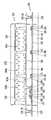
本実施形態では、図4の電気泳動表示装置を本発明の他の一実施形態による薄膜トランジスタ表示板を備える電気泳動表示装置に適用した場合について説明する。
図5及び図6は、本発明の他の一実施形態による電気泳動表示装置を示す断面図である。
本実施形態による電気泳動表示装置は、実施例1と同様に、薄膜トランジスタ表示板100、対向表示板200、及びこれらの間で隔壁360によって分離される複数の領域を備える。In the present embodiment, a case where the electrophoretic display device of FIG. 4 is applied to an electrophoretic display device including a thin film transistor array panel according to another embodiment of the present invention will be described.
5 and 6 are cross-sectional views illustrating an electrophoretic display device according to another embodiment of the present invention.
As in Example 1, the electrophoretic display device according to the present embodiment includes the thin film
まず、薄膜トランジスタ表示板100には、透明ガラスなどからなる下部基板110上にゲート電極124を有する複数のゲート線121が形成されている。
ゲート線121は、ゲート信号を伝達し、主に図において横方向に延設されている。各ゲート線121は、図下方に突出している複数のゲート電極124と他の層または外部駆動回路と接続するための面積が広い端部129を有する。First, in the thin film
The
ゲート線121上には、窒化ケイ素(SiNx)または酸化ケイ素(SiO2)からなるゲート絶縁膜140が形成されている。
ゲート絶縁膜140上には、水素化非晶質シリコン(非晶質シリコンはa−Si略称する)または多結晶シリコンなどからなる複数の線状半導体151が形成されている。線状半導体151は、主に図縦方向に延設されており、ゲート電極124側に延設された複数の突出部154を有する。A
A plurality of
線状半導体151上には、複数の線状及び島状オーミック接触部材161、165が形成されている。線状オーミック接触部材161は、複数の突出部163を有し、突出部163と島状オーミック接触部材165は、線状半導体の突出部154上で対をなしている。線状及び島状オーミック接触部材161、165は、リン(P)のようなn型不純物が高濃度にドーピングされているn+水素化非晶質シリコンなどの物質またはシリサイドで構成することができる。 A plurality of linear and island-shaped
オーミック接触部材161、165及びゲート絶縁膜140上には、複数のデータ線171及びデータ線171から分離されている複数のドレイン電極175が形成されている。
データ線171は、データ信号を伝達し、主に図縦方向に延設されてゲート線121と交差する。また、各データ線171は、ドレイン電極175側に突出した複数のソース電極173と他の層または外部駆動回路と接続するための広い面積の端部179を有する。A plurality of
The
ゲート電極124、ソース電極173及びドレイン電極175は、線状半導体151の突出部154と共に薄膜トランジスタ(TFT)をなし、薄膜トランジスタチャンネルは、ソース電極173とドレイン電極175との間の線状半導体151の突出部154上に形成される。
データ線171、ドレイン電極175及び露出した半導体部分上には、保護膜180が形成されている。保護膜180は、窒化ケイ素(SiNx)や酸化ケイ素(SiO2)などの無機絶縁物質、アクリル系またはイミド系などの感光性を有する有機絶縁物質、4.0以下の誘電定数を有し、プラズマ化学気相蒸着(PECVD)で形成されるa−Si:C:O、a−Si:O:Fなどから構成することができる。さらに、保護膜180は、有機膜の優れた絶縁特性を維持しつつ、露出した半導体部分に影響を及ぼさないように下部無機膜と上部有機膜からなる二重膜構造で形成することもできる。The
A
保護膜180は、データ線171の端部179とドレイン電極175の拡張部をそれぞれ露出する複数のコンタクトホール182、185を有する。
保護膜180上には、複数の画素電極190及び複数の接触補助部材81、82が形成されている。これらは、ITOまたはIZOなどの透明な導電物質、またはアルミニウム(Al)、銀(Ag)またはこれらの合金などの反射性導電物質から構成することができる。The
A plurality of
画素電極190は、コンタクトホール185を介してドレイン電極175と物理的、電気的に接続されている。
複数の接触補助部材81、82は、それぞれコンタクトホール181、182を介してゲート線121の端部129とデータ線171の端部179に接続されている。接触補助部材81、82は、ゲート線またはデータ線の端部129、179と外部装置との接着性を補完し、これらを保護する。The
The plurality of
一方、薄膜トランジスタ表示板100と対向する対向表示板200は、図5のように、透明ガラスなどからなる上部基板210、上部基板210上部に形成され、繰り返される凹パターンを有する共通電極270を備える。
または、図6のように、対向表示板200は、透明ガラスなどからなる上部基板210、上部基板210上部に形成され繰り返される凹凸を有する層間膜250、及び層間膜250全面に形成されている共通電極270を備える構成とすることもできる。この場合、感光性有機物質からなる層間膜250を露光して一定に繰り返される凹凸を形成することができ、前記凹凸によって各画素領域毎に繰り返される凹パターンを形成することができる。層間膜250上には、ITOまたはIZOのような透明導電体からなる共通電極270が形成されている。On the other hand, the
Alternatively, as shown in FIG. 6, the
前記のように、対向表示板200の共通電極270または層間膜250に繰り返される凹パターンが形成することによって、視野角をさらに改善することができる。
また、薄膜トランジスタ表示板100と対向表示板200との間には、各画素領域を分離するための複数の隔壁360が形成されている。
隔壁360によって分離された各画素領域は、透明な流体310、陽性または陰性に帯電された着色粒子300a、300b、300c及び黒色粒子300dを有する。流体310は、着色粒子300a、300b、300c及び黒色粒子300dを分散させるための媒質であって、着色粒子300a、300b、300c及び黒色粒子300dの移動を妨げない程度の十分に低い粘性及び誘電常数を有する必要がある。As described above, by forming a concave pattern repeated on the
In addition, a plurality of
Each pixel region separated by the
黒色粒子300dは、着色粒子300a、300b、300cと反対電荷を有するので、電界印加時に互いに反対電極側に配列される。例えば、1つの画素領域内の着色粒子300aが電気泳動現象によって画素電極190側に移動する時、反対の電荷を有する黒色粒子300dは、共通電極270側に移動することによって外部光が黒色粒子300dに吸収されて完全なブラックを表現することができる。その結果、コントラスト比を改善することができる。 Since the
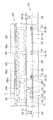
図7は、図6の電気泳動表示装置に電界を印加したときの図6のA部分を拡大して示した断面図である。
電界印加時、共通電極270または層間膜250に繰り返される凹パターンが形成されている場合、共通電極270と反対電荷を有する着色粒子300aは共通電極270の表面に沿って一列に分布する。これにより、各画素の正面だけでなく側面からも着色粒子330aによって反射される程度を調節し、視野角を顕著に向上させることができる。7 is an enlarged cross-sectional view of a portion A in FIG. 6 when an electric field is applied to the electrophoretic display device in FIG.
When a concave pattern is formed in the
以上、薄膜トランジスタを用いた能動型(active)駆動方式のみについて例を挙げて説明したが、交差して形成された2つの電極間に電圧を印加する手動型(passive)駆動方式にも同様に適用することができることは勿論である。
このように、隔壁によって分離された領域でそれぞれの着色粒子を含むことによって、追加工程が不要で、かつ別途のカラーフィルタなしで多様な色を表現することができ、一側の電極に凹部を有することによって、より改善された広視野角特性を実現することができる。As described above, only the active driving method using a thin film transistor has been described by way of example, but the present invention is similarly applied to a manual driving method in which a voltage is applied between two electrodes formed in an intersecting manner. Of course it can be done.
As described above, by including the respective colored particles in the region separated by the partition wall, an additional process is unnecessary, and various colors can be expressed without a separate color filter. By having it, a more improved wide viewing angle characteristic can be realized.
以上、本発明の好適な実施形態について詳細に説明したが、本発明の権利範囲はこれに限定されるものでなく、特許請求の範囲で定義している本発明の基本概念を利用した当業者の様々な変形及び改良形態も本発明の権利範囲に属する。 The preferred embodiment of the present invention has been described in detail above, but the scope of the present invention is not limited to this, and those skilled in the art using the basic concept of the present invention defined in the claims. Various modifications and improvements are also within the scope of the present invention.
100 薄膜トランジスタ表示板
110 下部基板
121 ゲート線
124 ゲート電極
140 ゲート絶縁膜
151 半導体
171 データ線
180 保護膜
190 画素電極
200 対向表示板
210 上部基板
250 層間膜
270 共通電極
300a〜300c 着色粒子
300d 黒色粒子
360 隔壁
310 流体100 Thin film
Claims (15)
Translated fromJapanese前記第1基板に対向する第2基板上に形成されている第2電極と、
前記第1電極と前記第2電極との間を複数の領域に分離する隔壁と、
前記各領域内に含まれ、赤色、緑色及び青色のいずれか一色で着色された複数の帯電粒子と、
を備える電気泳動表示装置。A first electrode formed on the first substrate;
A second electrode formed on a second substrate facing the first substrate;
A partition that separates a plurality of regions between the first electrode and the second electrode;
A plurality of charged particles that are included in each region and are colored with one of red, green, and blue; and
An electrophoretic display device comprising:
前記第1基板に対向する第2基板上に形成され凹部を有する第2電極と、
前記第1電極と前記第2電極との間を複数の領域に分離する隔壁と、
前記各領域内に含まれ、流体内に分散している複数の着色帯電粒子と、
を備えることを特徴とする、電気泳動表示装置。A first electrode formed on the first substrate;
A second electrode formed on a second substrate facing the first substrate and having a recess;
A partition that separates a plurality of regions between the first electrode and the second electrode;
A plurality of colored charged particles contained in each region and dispersed in a fluid;
An electrophoretic display device comprising:
Applications Claiming Priority (1)
| Application Number | Priority Date | Filing Date | Title |
|---|---|---|---|
| KR1020050029905AKR101143002B1 (en) | 2005-04-11 | 2005-04-11 | Electrophoretic display |
Publications (1)
| Publication Number | Publication Date |
|---|---|
| JP2006293312Atrue JP2006293312A (en) | 2006-10-26 |
Family
ID=37077570
Family Applications (1)
| Application Number | Title | Priority Date | Filing Date |
|---|---|---|---|
| JP2006020013APendingJP2006293312A (en) | 2005-04-11 | 2006-01-30 | Electrophoretic display device |
Country Status (5)
| Country | Link |
|---|---|
| US (1) | US7355784B2 (en) |
| JP (1) | JP2006293312A (en) |
| KR (1) | KR101143002B1 (en) |
| CN (1) | CN1847967B (en) |
| TW (1) | TW200636659A (en) |
Cited By (1)
| Publication number | Priority date | Publication date | Assignee | Title |
|---|---|---|---|---|
| JP2009175628A (en)* | 2008-01-28 | 2009-08-06 | Mitsubishi Pencil Co Ltd | Display device, power supply device, power supply method, and program |
Families Citing this family (24)
| Publication number | Priority date | Publication date | Assignee | Title |
|---|---|---|---|---|
| KR20080011873A (en)* | 2006-08-01 | 2008-02-11 | 삼성전자주식회사 | Electrophoresis display |
| KR101256023B1 (en)* | 2006-10-31 | 2013-04-18 | 삼성디스플레이 주식회사 | Electrophoretic display and the manufacturing method thereof |
| KR20080053035A (en)* | 2006-12-08 | 2008-06-12 | 삼성전자주식회사 | Electrophoretic display |
| KR20080061039A (en)* | 2006-12-28 | 2008-07-02 | 삼성전자주식회사 | Electrophoretic display device and manufacturing method thereof |
| JP2009145833A (en)* | 2007-12-18 | 2009-07-02 | Seiko Epson Corp | Electrophoretic display device and electronic apparatus |
| TWI418911B (en)* | 2008-12-01 | 2013-12-11 | Prime View Int Co Ltd | Electro-phoretic display and fabricating method thereof |
| KR101274154B1 (en)* | 2008-12-19 | 2013-06-13 | 엘지디스플레이 주식회사 | Electrophoretic display device using photo sensor |
| KR20090086192A (en)* | 2009-07-22 | 2009-08-11 | 주식회사 나노브릭 | Display Method and Device Using Photonic Crystallinity |
| CN102023453B (en)* | 2009-09-23 | 2012-10-10 | 鸿富锦精密工业(深圳)有限公司 | Electronic paper and display device thereof |
| KR101343800B1 (en)* | 2010-05-10 | 2013-12-20 | 엘지디스플레이 주식회사 | Electrophoretic display device and method of fabricating the same |
| US9013394B2 (en)* | 2010-06-04 | 2015-04-21 | E Ink California, Llc | Driving method for electrophoretic displays |
| KR101352907B1 (en)* | 2010-07-06 | 2014-01-21 | 엘지디스플레이 주식회사 | Electrophoretic display deivce and method of fabrication thereof |
| KR101687720B1 (en)* | 2010-07-14 | 2016-12-29 | 엘지디스플레이 주식회사 | Electrophoretic display device and method of fabrication thereof |
| KR20120022253A (en)* | 2010-09-01 | 2012-03-12 | 엘지디스플레이 주식회사 | Electrophoretic display deivce and method of fabrication thereof |
| US9213211B2 (en) | 2010-10-03 | 2015-12-15 | Hewlett-Packard Development Company, L.P. | Luminescent pixel assembly |
| JPWO2013099560A1 (en)* | 2011-12-27 | 2015-04-30 | 三菱電機株式会社 | Display device |
| US10726760B2 (en) | 2013-10-07 | 2020-07-28 | E Ink California, Llc | Driving methods to produce a mixed color state for an electrophoretic display |
| US10380931B2 (en) | 2013-10-07 | 2019-08-13 | E Ink California, Llc | Driving methods for color display device |
| TWI550332B (en) | 2013-10-07 | 2016-09-21 | 電子墨水加利福尼亞有限責任公司 | Driving methods for color display device |
| US9411374B2 (en)* | 2014-02-20 | 2016-08-09 | Amazon Technologies, Inc. | Electronic device display stack |
| EP3304539A4 (en)* | 2015-06-02 | 2018-11-21 | E Ink Corporation | Apparatus for driving displays |
| KR102413716B1 (en)* | 2017-09-25 | 2022-06-28 | 삼성디스플레이 주식회사 | Display panel |
| CN110320724A (en)* | 2019-07-22 | 2019-10-11 | 浙江富申科技有限公司 | A kind of block type multicolor displaying electrophoretic display apparatus |
| CN111627399A (en)* | 2020-06-16 | 2020-09-04 | 掌阅科技股份有限公司 | Method, terminal and computer readable storage medium capable of locally transforming display colors |
Citations (6)
| Publication number | Priority date | Publication date | Assignee | Title |
|---|---|---|---|---|
| JPH10123547A (en)* | 1996-10-17 | 1998-05-15 | Fuji Xerox Co Ltd | Image display device |
| JP2001174853A (en)* | 1999-12-16 | 2001-06-29 | Japan Science & Technology Corp | Electrophoretic display |
| JP2002099002A (en)* | 2000-09-21 | 2002-04-05 | Fuji Xerox Co Ltd | Image display medium |
| JP2002162651A (en)* | 2000-11-24 | 2002-06-07 | Seiko Epson Corp | Electrophoresis apparatus and method for manufacturing the same |
| JP2003161967A (en)* | 2001-11-27 | 2003-06-06 | Minolta Co Ltd | Reversible image display medium, manufacturing method therefor and image forming method |
| JP2003330047A (en)* | 2002-05-10 | 2003-11-19 | Seiko Epson Corp | Electro-optical device, method of manufacturing the same, and electronic apparatus |
Family Cites Families (34)
| Publication number | Priority date | Publication date | Assignee | Title |
|---|---|---|---|---|
| KR930005559B1 (en)* | 1991-06-14 | 1993-06-23 | 삼성전관 주식회사 | Plane display devices |
| US6124851A (en) | 1995-07-20 | 2000-09-26 | E Ink Corporation | Electronic book with multiple page displays |
| US5961804A (en) | 1997-03-18 | 1999-10-05 | Massachusetts Institute Of Technology | Microencapsulated electrophoretic display |
| US7075502B1 (en) | 1998-04-10 | 2006-07-11 | E Ink Corporation | Full color reflective display with multichromatic sub-pixels |
| JP2000035598A (en) | 1998-07-17 | 2000-02-02 | Nok Corp | Display panel |
| JP2000137250A (en) | 1998-11-04 | 2000-05-16 | Sony Corp | Display device and method for driving the display device |
| US6312304B1 (en)* | 1998-12-15 | 2001-11-06 | E Ink Corporation | Assembly of microencapsulated electronic displays |
| JP4385438B2 (en) | 1999-05-14 | 2009-12-16 | ブラザー工業株式会社 | Recording medium, electrophoretic display device, and control method of recording medium |
| JP2001324728A (en) | 2000-05-15 | 2001-11-22 | Seiko Epson Corp | Video playback paper, video playback method, and product using the same |
| JP3805180B2 (en)* | 2000-09-14 | 2006-08-02 | 株式会社東芝 | Display element |
| JP4865172B2 (en) | 2000-10-11 | 2012-02-01 | キヤノン株式会社 | Display device and manufacturing method thereof |
| JP3819721B2 (en) | 2001-03-21 | 2006-09-13 | 株式会社東芝 | Electrophoretic display device |
| JP2004520621A (en) | 2001-04-25 | 2004-07-08 | コーニンクレッカ フィリップス エレクトロニクス エヌ ヴィ | Electrophoretic color display device |
| JP4377554B2 (en) | 2001-05-29 | 2009-12-02 | Tdk株式会社 | Display device |
| US6788452B2 (en)* | 2001-06-11 | 2004-09-07 | Sipix Imaging, Inc. | Process for manufacture of improved color displays |
| TW552485B (en) | 2001-07-17 | 2003-09-11 | Sipix Imaging Inc | An improved electrophoretic display with in-plane switching |
| TW550529B (en)* | 2001-08-17 | 2003-09-01 | Sipix Imaging Inc | An improved electrophoretic display with dual-mode switching |
| WO2003019279A1 (en) | 2001-08-23 | 2003-03-06 | Koninklijke Philips Electronics N.V. | Electrophoretic display device |
| JP2003156770A (en) | 2001-11-22 | 2003-05-30 | Toppan Printing Co Ltd | Multicolor display panel and manufacturing method thereof |
| EP1478973B1 (en) | 2002-02-19 | 2008-07-23 | Koninklijke Philips Electronics N.V. | Electrophoretic display device |
| JP4207448B2 (en) | 2002-04-02 | 2009-01-14 | 凸版印刷株式会社 | Display method for multicolor display panel and method for manufacturing multicolor display panel |
| JP3645228B2 (en) | 2002-04-17 | 2005-05-11 | 株式会社東芝 | Receiver |
| US6806343B2 (en) | 2002-05-31 | 2004-10-19 | Certainteed Corporation | Method of preparing a stable, low pH phenolic resin |
| JP2004012656A (en) | 2002-06-05 | 2004-01-15 | Hitachi Maxell Ltd | Display device using electrophoretic particles |
| KR100438901B1 (en) | 2002-08-09 | 2004-07-02 | 한국전자통신연구원 | Electrophoretic display |
| JP2004094137A (en)* | 2002-09-04 | 2004-03-25 | Hitachi Ltd | Image display medium, method of manufacturing and disassembling method |
| US6930668B2 (en) | 2003-01-15 | 2005-08-16 | Xerox Corporation | Color-enabled electrophoretic display and medium |
| JP2004271610A (en) | 2003-03-05 | 2004-09-30 | Canon Inc | Color electrophoretic display |
| KR100513085B1 (en) | 2003-03-25 | 2005-09-07 | 경북대학교 산학협력단 | Method of panel fabrication for microencapsulated electrophoretic display driven by External Field |
| KR100951351B1 (en) | 2003-04-22 | 2010-04-08 | 삼성전자주식회사 | Thin film transistor array panel and electrophoretic display device including the same |
| JP2005037851A (en)* | 2003-06-24 | 2005-02-10 | Seiko Epson Corp | Electrophoretic dispersion liquid, electrophoretic display device, electrophoretic display device manufacturing method, and electronic apparatus |
| JP2005242320A (en)* | 2004-01-27 | 2005-09-08 | Canon Inc | Display device and display method thereof |
| KR20050112878A (en)* | 2004-05-28 | 2005-12-01 | 삼성전자주식회사 | Electro phoretic indication display |
| US20060215252A1 (en)* | 2005-03-25 | 2006-09-28 | Fuji Xerox Co., Ltd. | Display medium, display device, and display method |
- 2005
- 2005-04-11KRKR1020050029905Apatent/KR101143002B1/ennot_activeExpired - Lifetime
- 2005-11-08TWTW094139061Apatent/TW200636659A/enunknown
- 2005-11-25CNCN2005101272112Apatent/CN1847967B/enactiveActive
- 2006
- 2006-01-30JPJP2006020013Apatent/JP2006293312A/enactivePending
- 2006-03-07USUS11/369,683patent/US7355784B2/enactiveActive
Patent Citations (6)
| Publication number | Priority date | Publication date | Assignee | Title |
|---|---|---|---|---|
| JPH10123547A (en)* | 1996-10-17 | 1998-05-15 | Fuji Xerox Co Ltd | Image display device |
| JP2001174853A (en)* | 1999-12-16 | 2001-06-29 | Japan Science & Technology Corp | Electrophoretic display |
| JP2002099002A (en)* | 2000-09-21 | 2002-04-05 | Fuji Xerox Co Ltd | Image display medium |
| JP2002162651A (en)* | 2000-11-24 | 2002-06-07 | Seiko Epson Corp | Electrophoresis apparatus and method for manufacturing the same |
| JP2003161967A (en)* | 2001-11-27 | 2003-06-06 | Minolta Co Ltd | Reversible image display medium, manufacturing method therefor and image forming method |
| JP2003330047A (en)* | 2002-05-10 | 2003-11-19 | Seiko Epson Corp | Electro-optical device, method of manufacturing the same, and electronic apparatus |
Cited By (1)
| Publication number | Priority date | Publication date | Assignee | Title |
|---|---|---|---|---|
| JP2009175628A (en)* | 2008-01-28 | 2009-08-06 | Mitsubishi Pencil Co Ltd | Display device, power supply device, power supply method, and program |
Also Published As
| Publication number | Publication date |
|---|---|
| TW200636659A (en) | 2006-10-16 |
| CN1847967A (en) | 2006-10-18 |
| CN1847967B (en) | 2011-02-16 |
| KR101143002B1 (en) | 2012-05-08 |
| KR20060107670A (en) | 2006-10-16 |
| US20060244715A1 (en) | 2006-11-02 |
| US7355784B2 (en) | 2008-04-08 |
Similar Documents
| Publication | Publication Date | Title |
|---|---|---|
| JP2006293312A (en) | Electrophoretic display device | |
| USRE50119E1 (en) | Liquid crystal display and method of fabricating the same having particular data signal transmission lines | |
| CN102193261B (en) | Liquid crystal display | |
| US7952558B2 (en) | Methods for driving electrophoretic display so as to avoid persistent unidirectional current through TFT switches | |
| JP5351498B2 (en) | Liquid crystal display device and driving method thereof | |
| CN107357105A (en) | A kind of array base palte, display panel, display device | |
| CN101025530B (en) | Display panel and method of forming thereof | |
| CN101017294B (en) | Liquid crystal display device | |
| KR20070121403A (en) | Electrophoretic display device and manufacturing method thereof | |
| KR20080008858A (en) | Thin film transistor array panel | |
| KR20040091480A (en) | Thin film transistor array panel and electro phoretic indication display including the panel | |
| JP2012163948A (en) | Liquid crystal display device | |
| KR20080101582A (en) | Liquid crystal display | |
| CN101201516B (en) | Increasing LCD aperture ratios | |
| KR20080006036A (en) | Eletrophoretic display apparatus | |
| KR20080102798A (en) | Liquid crystal display | |
| KR20060030630A (en) | Electrophoretic display device and manufacturing method thereof | |
| KR20160086525A (en) | Liquid crystal display device | |
| US7839463B2 (en) | Thin film diode panel and manufacturing method of the same | |
| KR20080046960A (en) | Electrophoretic display device and manufacturing method thereof | |
| KR20060080761A (en) | Thin film transistor array panel and liquid crystal display including the same | |
| KR20060081153A (en) | Thin film transistor array panel and liquid crystal display including the same | |
| KR20080076543A (en) | Electrophoretic display | |
| KR20080064343A (en) | Liquid crystal display and driving method thereof | |
| KR20080029068A (en) | Electrophoresis display |
Legal Events
| Date | Code | Title | Description |
|---|---|---|---|
| A621 | Written request for application examination | Free format text:JAPANESE INTERMEDIATE CODE: A621 Effective date:20081126 | |
| A131 | Notification of reasons for refusal | Free format text:JAPANESE INTERMEDIATE CODE: A131 Effective date:20110705 | |
| A521 | Request for written amendment filed | Free format text:JAPANESE INTERMEDIATE CODE: A523 Effective date:20110819 | |
| RD02 | Notification of acceptance of power of attorney | Free format text:JAPANESE INTERMEDIATE CODE: A7422 Effective date:20110819 | |
| A131 | Notification of reasons for refusal | Free format text:JAPANESE INTERMEDIATE CODE: A131 Effective date:20120221 | |
| A02 | Decision of refusal | Free format text:JAPANESE INTERMEDIATE CODE: A02 Effective date:20120710 |