JP2006286639A - Light emitting device having a plurality of overlapping panels forming recess for emitting light - Google Patents
Light emitting device having a plurality of overlapping panels forming recess for emitting lightDownload PDFInfo
- Publication number
- JP2006286639A JP2006286639AJP2006097375AJP2006097375AJP2006286639AJP 2006286639 AJP2006286639 AJP 2006286639AJP 2006097375 AJP2006097375 AJP 2006097375AJP 2006097375 AJP2006097375 AJP 2006097375AJP 2006286639 AJP2006286639 AJP 2006286639A
- Authority
- JP
- Japan
- Prior art keywords
- light
- substrate
- emitting device
- light emitting
- recesses
- Prior art date
- Legal status (The legal status is an assumption and is not a legal conclusion. Google has not performed a legal analysis and makes no representation as to the accuracy of the status listed.)
- Pending
Links
Images


Classifications
- G—PHYSICS
- G02—OPTICS
- G02F—OPTICAL DEVICES OR ARRANGEMENTS FOR THE CONTROL OF LIGHT BY MODIFICATION OF THE OPTICAL PROPERTIES OF THE MEDIA OF THE ELEMENTS INVOLVED THEREIN; NON-LINEAR OPTICS; FREQUENCY-CHANGING OF LIGHT; OPTICAL LOGIC ELEMENTS; OPTICAL ANALOGUE/DIGITAL CONVERTERS
- G02F1/00—Devices or arrangements for the control of the intensity, colour, phase, polarisation or direction of light arriving from an independent light source, e.g. switching, gating or modulating; Non-linear optics
- G02F1/01—Devices or arrangements for the control of the intensity, colour, phase, polarisation or direction of light arriving from an independent light source, e.g. switching, gating or modulating; Non-linear optics for the control of the intensity, phase, polarisation or colour
- G02F1/13—Devices or arrangements for the control of the intensity, colour, phase, polarisation or direction of light arriving from an independent light source, e.g. switching, gating or modulating; Non-linear optics for the control of the intensity, phase, polarisation or colour based on liquid crystals, e.g. single liquid crystal display cells
- G02F1/133—Constructional arrangements; Operation of liquid crystal cells; Circuit arrangements
- G02F1/1333—Constructional arrangements; Manufacturing methods
- G02F1/1335—Structural association of cells with optical devices, e.g. polarisers or reflectors
- G—PHYSICS
- G02—OPTICS
- G02B—OPTICAL ELEMENTS, SYSTEMS OR APPARATUS
- G02B6/00—Light guides; Structural details of arrangements comprising light guides and other optical elements, e.g. couplings
- G02B6/0001—Light guides; Structural details of arrangements comprising light guides and other optical elements, e.g. couplings specially adapted for lighting devices or systems
- G02B6/0011—Light guides; Structural details of arrangements comprising light guides and other optical elements, e.g. couplings specially adapted for lighting devices or systems the light guides being planar or of plate-like form
- G02B6/0033—Means for improving the coupling-out of light from the light guide
- G02B6/005—Means for improving the coupling-out of light from the light guide provided by one optical element, or plurality thereof, placed on the light output side of the light guide
- G—PHYSICS
- G02—OPTICS
- G02B—OPTICAL ELEMENTS, SYSTEMS OR APPARATUS
- G02B6/00—Light guides; Structural details of arrangements comprising light guides and other optical elements, e.g. couplings
- G02B6/0001—Light guides; Structural details of arrangements comprising light guides and other optical elements, e.g. couplings specially adapted for lighting devices or systems
- G02B6/0011—Light guides; Structural details of arrangements comprising light guides and other optical elements, e.g. couplings specially adapted for lighting devices or systems the light guides being planar or of plate-like form
- G02B6/0066—Light guides; Structural details of arrangements comprising light guides and other optical elements, e.g. couplings specially adapted for lighting devices or systems the light guides being planar or of plate-like form characterised by the light source being coupled to the light guide
- G02B6/0068—Arrangements of plural sources, e.g. multi-colour light sources
- G—PHYSICS
- G02—OPTICS
- G02B—OPTICAL ELEMENTS, SYSTEMS OR APPARATUS
- G02B6/00—Light guides; Structural details of arrangements comprising light guides and other optical elements, e.g. couplings
- G02B6/0001—Light guides; Structural details of arrangements comprising light guides and other optical elements, e.g. couplings specially adapted for lighting devices or systems
- G02B6/0011—Light guides; Structural details of arrangements comprising light guides and other optical elements, e.g. couplings specially adapted for lighting devices or systems the light guides being planar or of plate-like form
- G02B6/0075—Arrangements of multiple light guides
- G02B6/0078—Side-by-side arrangements, e.g. for large area displays
- G02B6/008—Side-by-side arrangements, e.g. for large area displays of the partially overlapping type
- G—PHYSICS
- G02—OPTICS
- G02B—OPTICAL ELEMENTS, SYSTEMS OR APPARATUS
- G02B6/00—Light guides; Structural details of arrangements comprising light guides and other optical elements, e.g. couplings
- G02B6/0001—Light guides; Structural details of arrangements comprising light guides and other optical elements, e.g. couplings specially adapted for lighting devices or systems
- G02B6/0011—Light guides; Structural details of arrangements comprising light guides and other optical elements, e.g. couplings specially adapted for lighting devices or systems the light guides being planar or of plate-like form
- G02B6/0081—Mechanical or electrical aspects of the light guide and light source in the lighting device peculiar to the adaptation to planar light guides, e.g. concerning packaging
- G02B6/0085—Means for removing heat created by the light source from the package
- G—PHYSICS
- G02—OPTICS
- G02F—OPTICAL DEVICES OR ARRANGEMENTS FOR THE CONTROL OF LIGHT BY MODIFICATION OF THE OPTICAL PROPERTIES OF THE MEDIA OF THE ELEMENTS INVOLVED THEREIN; NON-LINEAR OPTICS; FREQUENCY-CHANGING OF LIGHT; OPTICAL LOGIC ELEMENTS; OPTICAL ANALOGUE/DIGITAL CONVERTERS
- G02F1/00—Devices or arrangements for the control of the intensity, colour, phase, polarisation or direction of light arriving from an independent light source, e.g. switching, gating or modulating; Non-linear optics
- G02F1/01—Devices or arrangements for the control of the intensity, colour, phase, polarisation or direction of light arriving from an independent light source, e.g. switching, gating or modulating; Non-linear optics for the control of the intensity, phase, polarisation or colour
- G02F1/13—Devices or arrangements for the control of the intensity, colour, phase, polarisation or direction of light arriving from an independent light source, e.g. switching, gating or modulating; Non-linear optics for the control of the intensity, phase, polarisation or colour based on liquid crystals, e.g. single liquid crystal display cells
- G02F1/133—Constructional arrangements; Operation of liquid crystal cells; Circuit arrangements
- G02F1/1333—Constructional arrangements; Manufacturing methods
- G02F1/1335—Structural association of cells with optical devices, e.g. polarisers or reflectors
- G02F1/1336—Illuminating devices
- G02F1/133615—Edge-illuminating devices, i.e. illuminating from the side
- G—PHYSICS
- G02—OPTICS
- G02F—OPTICAL DEVICES OR ARRANGEMENTS FOR THE CONTROL OF LIGHT BY MODIFICATION OF THE OPTICAL PROPERTIES OF THE MEDIA OF THE ELEMENTS INVOLVED THEREIN; NON-LINEAR OPTICS; FREQUENCY-CHANGING OF LIGHT; OPTICAL LOGIC ELEMENTS; OPTICAL ANALOGUE/DIGITAL CONVERTERS
- G02F1/00—Devices or arrangements for the control of the intensity, colour, phase, polarisation or direction of light arriving from an independent light source, e.g. switching, gating or modulating; Non-linear optics
- G02F1/01—Devices or arrangements for the control of the intensity, colour, phase, polarisation or direction of light arriving from an independent light source, e.g. switching, gating or modulating; Non-linear optics for the control of the intensity, phase, polarisation or colour
- G02F1/13—Devices or arrangements for the control of the intensity, colour, phase, polarisation or direction of light arriving from an independent light source, e.g. switching, gating or modulating; Non-linear optics for the control of the intensity, phase, polarisation or colour based on liquid crystals, e.g. single liquid crystal display cells
- G02F1/133—Constructional arrangements; Operation of liquid crystal cells; Circuit arrangements
- G02F1/1333—Constructional arrangements; Manufacturing methods
- G02F1/1335—Structural association of cells with optical devices, e.g. polarisers or reflectors
- G02F1/1336—Illuminating devices
- G02F1/133602—Direct backlight
- G02F1/133603—Direct backlight with LEDs
Landscapes
- Physics & Mathematics (AREA)
- General Physics & Mathematics (AREA)
- Optics & Photonics (AREA)
- Nonlinear Science (AREA)
- Mathematical Physics (AREA)
- Chemical & Material Sciences (AREA)
- Crystallography & Structural Chemistry (AREA)
- Planar Illumination Modules (AREA)
- Fastening Of Light Sources Or Lamp Holders (AREA)
- Liquid Crystal (AREA)
- Arrangement Of Elements, Cooling, Sealing, Or The Like Of Lighting Devices (AREA)
- Led Device Packages (AREA)
Abstract
Description
Translated fromJapanese本発明はLCD等の表示装置に使用される発光装置に関する。 The present invention relates to a light emitting device used for a display device such as an LCD.
透過型液晶ディスプレイ(LCD)は照明としてバックライトを必要とするディスプレイである。バックライトは通常、透過面、反射面、及び複数の縁部を有する概ね平坦な光導波路からなる。1以上の光源からの光は光導波路の縁部に入射するように照射され、光導波路の反射面で反射され、光導波路の透過面を通して放射される。光源には、冷陰極蛍光灯(CCFL)や発光ダイオード(LED)アレイのように様々な形がある。 A transmissive liquid crystal display (LCD) is a display that requires a backlight as illumination. A backlight typically consists of a generally flat optical waveguide having a transmissive surface, a reflective surface, and a plurality of edges. Light from one or more light sources is irradiated so as to enter the edge of the optical waveguide, is reflected by the reflection surface of the optical waveguide, and is emitted through the transmission surface of the optical waveguide. There are various types of light sources such as cold cathode fluorescent lamps (CCFL) and light emitting diode (LED) arrays.
例えば1以上の光導波路の縁部に隣接して配置された1以上のCCFL又はLEDアレイにより、バックライトの光導波路の縁部から光を当てる場合がある。このような縁部照明(エッジリット)型の光導波路の詳細については、特許文献1及び特許文献2に開示されている。 For example, one or more CCFLs or LED arrays arranged adjacent to the edge of one or more optical waveguides may shine light from the edge of the backlight optical waveguide. Details of such edge-lit optical waveguides are disclosed in Patent Document 1 and Patent Document 2.
他の場合では、例えば光導波路の反射面の下に配置された1以上のCCFL又はLEDアレイにより、バックライトの光導波路の底部から光を当てる場合がある。これらの光源は一次光導波路の下に配置された二次光導波路の中に光を照射する。二次導波路を出た光は反射され、一次光導波路の1以上の縁部に入射する。このような底部照明(ボトムリット)型の光導波路の詳細については、特許文献3に開示されている。
一実施形態において発光装置は(1)複数の重なり合うパネルに交差する仮想的表面に対して鋭角をなす複数の重なり合うパネルと、(2)重なり合うパネルの重なり部分の間に形成された複数の凹部とを備えた基板を有する。凹部は基板の第1の面に対して開口し、基板の第1の面は反射面を有する。複数の光源は凹部から光を放射するように配置される。 In one embodiment, the light emitting device includes: (1) a plurality of overlapping panels that form an acute angle with respect to a virtual surface that intersects the plurality of overlapping panels; and (2) a plurality of recesses formed between overlapping portions of the overlapping panels. Having a substrate. The recess opens to the first surface of the substrate, and the first surface of the substrate has a reflective surface. The plurality of light sources are arranged to emit light from the recess.
他の実施形態も開示する。 Other embodiments are also disclosed.
図1は液晶ディスプレイ(LCD)100の正面図である。LCD100は、複数のLCD素子を有するLCDパネル102、及びLCDパネル102の背面に配置されたバックライト104を有する。バックライト104はLCDパネル102を通して光を照射するように配置される。任意選択で、LCD100は、LCDパネル102とバックライト104の間に光調整器106、108、110を備える場合がある。光調整器は、1以上の光拡散層(例えば拡散器106)、1以上のプリズム層(例えば輝度上昇フィルム(BEF)108)及び/又は1以上の偏光層(例えば二重輝度上昇フィルム(DBEF)110)を含む場合がある。光調整層106、108、110は、素子の形に形成しても、シートの形に形成しても、フィルムの形に形成してもよく、LCDパネル102とバックライト104のどちらかに付着させてもよいし、両方の間に配置してもよい。 FIG. 1 is a front view of a liquid crystal display (LCD) 100. The
図1及び図2に示すように、バックライト104は、重なり合うパネル114、116、118に交差する仮想的表面120に対して鋭角をなす複数の重なり合う114、116、118と、重なり合うパネル114、116、118の重なり部分128、130の間に形成された複数の凹部122、124、126とを備えた基板112を有する。凹部122、124、126は、反射面132、134、136を有する基板112の面に対して開口している。 As shown in FIGS. 1 and 2, the
バックライト104は複数の光源138、140、142を有し、それらは凹部122、124、126から光を放射するように配置される。場合によっては、光源138、140、142は凹部122、124、126の中に配置されることもある。また、光源138、140、142は、凹部122、124、126の中へ延びるように配置してもよいし、凹部122、124、126の中へ光を照射するように配置してもよい。光源122、124、126は、その放射光の少なくとも一部が、凹部122、124、126の突出面144、146、148によって遮られるように配置することが望ましい。突出面144、146、148は反射性である。従って、光源122、124、126から発せられた光線は(1)凹部122、124、126の表面144、146、148、150、152、154で主に反射され、(2)基板112の反射面132、134、136でも反射される。 The
一実施形態において光調整器106は基板112の反射面132、134、136の上に配置され、基板112から反射された光を調整して透過する。光源138、140、142の位置、並びに凹部122、124、126の高さ及び幅は、光源138、140、142から放射された光線が、光調整器106の表面174に対して垂直から実質的に角度(θ1)で表面174に入射するように選択される。従って、光源138、140、142から直接放射された光の大部分は(A)光調整器106の表面174、及び(B)基板112の反射面132、134、136において複数回反射される。このようして、光(λ)は(1)空洞部156、(2)基板の反射面132、134、136の特性、及び(3)光調整器の表面174の特性により良好に分散され、及び/又は混色される。大抵の場合、光分散及び/又は混色を良好にすることにより、バックライト104から放射されるバックライトの色や照度の均一性を高めることができる。In one embodiment, the
バックライト104の周囲を画定している垂直面158、160、162は反射性であることが好ましく、バックライト104の周囲から外へ光が漏れないようにすることが好ましい。 The
図1及び図3に示すように、基板112は複数の同じ部材114、116、118から構成される。代替実施形態において、基板112は図4に示すように複数の異なる部材400、402から構成される場合もあり、また一体型の要素(図示せず)として構成される場合もある。 As shown in FIGS. 1 and 3, the
バックライト104用の基板112は種々の材料から形成することができ、例えばアルミニウムのような金属から形成される。基板材料(複数の場合もあり)には、実質的に剛性で熱伝導性の構造が得られるような材料が選択される。このようにすれば、基板112を利用して、反射面132、134、136に光線が当たることによって発生する熱を発散させることができる。さらに多くの熱発散素子(例えばヒートシンク164、166、168)が必要な場合、熱発散素子は基板112の概ね水平な面又は概ね垂直な面に取り付けることができ、また、両方の面に取り付けてもよい。ただし、図示の熱発散素子のタイプや形は例にすぎないことに注意して欲しい。 The
空洞部156の中で光を分散及び/又は混色するために、基板112の反射面132、134、136は様々な形に形成される場合がある。例えば、基板112の反射面132、134、136は拡散反射面であっても、鏡面反射面であっても、偏光反射面であってもよく、あるいは、それらの組み合わせであってもよい。凹部122内側の対向する反射面144、150のような種々の反射面は様々な形に形成される場合がある。 In order to disperse and / or mix light within the
一実施形態において、拡散反射面は一様な拡散反射面(即ち、表面のどの地点においても同じ拡散が得られるような拡散面)の形に形成される。他の実施形態において、拡散反射面は、拡散反射面のドットパターンとして形成される場合がある。後者の実施形態の場合、ドットパターンを外れた光を空洞部156の中へ戻すために、ドットパターンの下に鏡面反射層を配置する場合がある。この鏡面反射層は、例えば鏡面コーティングの形に形成される場合もあれば、基板112に付着させたフィルムの形に形成される場合もある。 In one embodiment, the diffuse reflective surface is formed in the form of a uniform diffuse reflective surface (i.e., a diffuse surface that provides the same diffusion at any point on the surface). In other embodiments, the diffuse reflection surface may be formed as a dot pattern of the diffuse reflection surface. In the case of the latter embodiment, a specular reflection layer may be disposed under the dot pattern in order to return light outside the dot pattern into the
図3に示すように、バックライト104の重なり合うパネル114、116、118はそれぞれ、重なり合うパネル114、116、118に交差する仮想的表面120に対して角度θ2を形成する。一実施形態においてバックライト104は、角度θ2が0度〜30度に設定される。As shown in FIG. 3, the
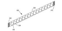
バックライト104の光源138、140、142は、何らかの単一の種々の形に形成される場合もあれば、種々の形の組み合わせとして形成される場合もある。一実施形態において、光源138、140、142は、図5に示すように発光ダイオード(LED)のアレイ500として形成される。アレイ500を構成するLED(例えば502、504)は、同じ色であってもよいし、違う色であってもよい。例えば、LEDアレイ500は、各LEDが赤色又は緑色又は青色を発する複数の異なる色のLED502、504を有する場合がある。LEDアレイ500が異なる色のLED502、504を有する場合、異なる色のLED502、504の駆動信号を調節することで、LEDアレイ500から放射される混合光の色点を調節することができる。 The
LEDの適当な組み合わせにおいて、異なる色のLEDは主に、波長450〜490nm(青っぽい光)、510〜550nm(緑っぽい光)、及び610〜650nm(赤っぽい光)の光を発する。LEDの他の適当な組み合わせにおいて、異なる色のLEDは主に、450〜480nm(青っぽい光)、480〜520nm(青緑色の光)、520〜550nm(緑っぽい光)、及び610〜650nm(赤っぽい光)の光を発する。 In a suitable combination of LEDs, the different colored LEDs mainly emit light with a wavelength of 450-490 nm (bluish light), 510-550 nm (greenish light), and 610-650 nm (reddish light). In other suitable combinations of LEDs, the different colored LEDs are mainly 450-480 nm (blue light), 480-520 nm (blue green light), 520-550 nm (green light), and 610-650 nm ( A reddish light is emitted.
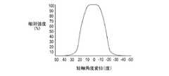
一実施形態においてLEDの光強度空間分布(配光)はLEDの光軸を中心として回転対称である。水平断面が円形のLEDは一般にそうなっている。代替実施形態においてLED600は図6〜図9に示すように楕円型の光強度空間分布を有する場合があり、長軸と短軸において光強度空間分布は異なる場合がある。例えば、図6及び図7に示す楕円型LEDの長軸と短軸における光強度のグラフを見て欲しい。楕円配光のLED600は、LEDの長軸がバックライト104の比較的薄い平面に対して実質的に水平な向きになるように配置し、LEDの短軸がバックライト104の平面に対して実質的に垂直な向きになるように配置すると有利である。その場合、LED600は基板112のより幅の広い「ストリップ」を照らすことができ、LED間の隙間により生じる光のバンディング(縞模様)の影響を低減することができる。また、楕円配光のLEDによれば、アレイ500に必要なLEDの数を減らすことができる場合もある。 In one embodiment, the light intensity spatial distribution (light distribution) of the LED is rotationally symmetric about the optical axis of the LED. This is generally the case for LEDs with a circular horizontal cross section. In an alternative embodiment, the
深さが浅く、比較的広い面積を有するバックライトの場合(例えば、LCDテレビのバックライトなど)、楕円型LED600を備えた複数の重なり合うパネルからなる基板を有するバックライト104に、短軸の光強度空間分布において視角20度〜90度を有し、長軸の光強度空間分において視角60度〜180度を有する楕円型LED600を取り付けると有利であることが、実験から分かっている。 In the case of a backlight having a shallow depth and a relatively large area (for example, a backlight of an LCD TV), a short-axis light is applied to the
バックライト104の光源138、140、142は種々の形に形成することができる。例えば、光源138は、LED502、504のアレイ500の形に形成され、電気接点508、510を備えた基板506上にそれらが取り付けられる場合がある(例えば図5に示すように)。このLED基板506は基板112に取り付けてもよいし、基板112の近くに取り付けてもよい。 The
一実施形態においてLED502、504を取り付ける基板506は可撓性プリント基板(FPC)である。他の実施形態において、LED502、504を取り付ける基板506はメタルコアプリント回路基板(MCPCB)である。後者の場合、MCPCBはLED基板506としての働きをするだけでなく、基板112の一部としても機能する。その他に、FPCのような基板506を内部に誘電体が挿入されたアルミニウム基板に取り付ける(接着する)場合もある。 In one embodiment, the
LED502、504は基板506に対して種々の方法で取り付けることができ、例えば、スルーホールや表面実装のような方法がある。図10は、スルーホールLED1000を基板1002に取り付ける例を示している。図11及び図12は2つの異なる表面実装型LED1100、1200を基板1102、1202に取り付ける例を示している(第1のLED1100は底部に一対のパッド1104、1106を備え、第2のLED1200はLEDパッケージの縁部の下にLEDパッケージを取り囲むように一対の接点1204、1206を備えている)。図10〜図12に示すLED1000、1100、1200を使用した場合、LEDの光軸は基板1002、1102、1202から垂直方向に延びる点に注意して欲しい。 The
図13は、ライトアングル・スルーホールLED1300を基板1302に取り付ける例を示している。図示のように、LED1300は、LED1300を取り付ける基板1302の縁部から突出するように取り付けられる。場合によっては、LED1300は空洞部156にもっと近い位置に(空洞部156の中へ延びるように)取り付けてもよい。図14及び図15は、種々のライトアングル表面実装LED1400、1500を基板1402、1502に取り付ける例を示している。図13〜図15に示すLED1300、1400、1500の光軸はそれぞれ、基板1302、1402、1502に対して平行な方向に延びている点に注意して欲しい。 FIG. 13 shows an example in which the right angle through-
図5に示すLEDアレイ500はLED502、504の行を1本しか有していないが、LEDアレイ500はLEDの行を複数有することもでき、光強度や色の一様な(又は一様でない)空間分布を実現することが望ましい場合、アレイ500を形成するLEDのタイプに応じて、複数の行により平行な列を形成したり、異なる行のLEDによりジグザグその他のパターンを形成してもよい。 Although the
図17及び図18は、パッケージLED502、504を基板506に取り付ける代替実施形態を示している。図示のように、複数のLEDチップ1700、1702が基板1704に取り付けられ、表面実装及び/又はワイヤボンディングを使用して、LEDチップ1700、1702が基板1704上のトレース又はパッドに電気的に接続される。LEDチップ1700、1702を保護するとともに、レンズを形成するために、LEDチップ1700、1702の上には、カプセル材料1706が形成される。カプセル材料1706は種々の製造方法によって形成することができ、例えば、グローブトップ、モールディング、キャスティング、真空印刷封止のような方法がある。一実施形態において、LEDチップ1700、1702を形成する基板1704は可撓性プリント基板(FPC)に取り付けられる。他の実施形態において、LED1700、1702を形成する基板1704はメタルコアプリント回路基板(MCPCB)に取り付けられる。後者の場合、MCPCBはLEDチップ基板1704としての働きをするだけでなく、基板112の一部としても機能する。その他に、FPCのような基板1704を内部に誘電体が挿入されたアルミニウム基板に取り付ける(接着する)場合もある。 17 and 18 show an alternative embodiment in which
一実施形態において、LED502、504やLEDチップ1700、1702のアレイは、基板112を形成する複数の重なり合うパネル114、116、118のうちの一枚に対して実質的に垂直に取り付けられる。代替又は追加として、LED1300、1400、1500のアレイが、基板116の反射面152、又は、凹部124のうちの1つにおける突出面146の1つに取り付けられる場合がある。ただし、光源138、140、142は全て凹部に配置することが望ましい。図16に示すように、異なるLEDタイプのアレイ1602、1604、1606を凹部122内の全ての表面に取り付けてもよい。 In one embodiment, the array of
前述のように、1以上の熱発散素子164、166、168をバックライト104に接続する場合がある。例えば、熱発散素子164、166、168は、光源138、140、142の近くに取り付けてもよいし、基板の反射面132、134、136とは反対側の面に取り付けてもよい。図1〜図3に示すように、熱発散素子164、166、168は基板112に結合される。ただし、熱発散素子164、166、168は、光源138、140、142を取り付ける1以上の基板506に対して(更に、又は代わりに)直接結合してもよい。 As described above, one or more
熱発散素子164、166、168は、対流と放射によりバックライト104から熱を奪い去ることができる。一実施形態において、熱発散素子164、166、168は、エアギャップ170により互いに隔離された複数のフィン(羽)を有する。LCD100及びバックライト104の使用時にフィン間のギャップの向きが重力の方向に一致するような向きにフィンを配置すれば、熱い空気はエアギャップ170から立ち昇り、エアギャップ170の底部から冷たい空気が引き込まれる。 The
一実施形態において、バックライト104は、その外縁部158、160、162の付近に取り付けられた(即ち付着された)反射性の素子、フィルム、又はコーティングを有する。図2を参照して欲しい。このようにすれば、バックライト104の外縁部158、160、162を光線が通過したり、外縁部によって光線が吸収されたり、外縁部によって光線が反射され、バックライト104の中に戻されたりすることを防止することができる。例えば、こうした反射性の素子、フィルム、又はコーティングには、光拡散性又は光反射性のものが使用される。 In one embodiment, the
図19は、代替実施形態によるバックライト1900を示している。この実施形態では、光調整器1902、1904が、バックライト1900の凹部1906、1908に、又は凹部の付近に配置される。このようにすれば、光源1910、1912によって放射された光を光調節器1902、1904によって受光し、調整することができる。例えば、光調整器1902、1904は1以上の素子、シート、又はフィルムからなり、それらが光拡散器、ホログラフィック光拡散器、又はプリズムとして機能する。一実施形態において、光調整器1902、1904は、様々な色のLEDから放射された光を前もって混合しておくのに便利な場合がある。 FIG. 19 shows a
図1〜図3及び図19に示した装置はバックライトを例として記載されているが、この装置は発光装置を必要とする様々な用途に利用することが可能である。例えば、ムード照明やタイル状光源も、バックライト104と同様にして構成される場合がある。 Although the device shown in FIGS. 1 to 3 and FIG. 19 is described using a backlight as an example, this device can be used for various applications that require a light emitting device. For example, mood lighting and tile light sources may be configured in the same manner as the
バックライト104は、その構成によっては、他の照明手段に比べて種々の利点が得られる。例えば、バックライト104は、一部のバックライトに比べて、バックライトとして光を放射するための表面を増加させることができる(そして、増加された表面はバックライトの表面にわたって分散される)。また、バックライト104の周囲からだけでなく、バックライト104の内部の位置からも光がバックライトとして放射される場合、バックライトの生成に使用される光源138、140、142には、200(mW)未満の消費電力を有するLEDのような、低消費電力のLEDを使用することもできる。そのため、光源138、140、142のコストが低減されるだけでなく(1)バックライト表面の正方形領域あたりの消費電力を低減することができ、(2)バックライトから発生する熱の量を低減することができ、(3)光源の効率を向上させることができ、(4)ディスプレイシステムの有機成分やポリマー成分の寿命を延ばすことができる。 Depending on the configuration of the
また、低消費電力の光源は小型の形状であることが多いため、光源を正確な中心間距離で配置することが可能である。異なる色の光(例えば、赤、緑、青の光)の混合を利用するバックライトの場合、光源を互いに近接して配置することができるため、バックライトの光放射面で光が屈折される前にそれらの光が完全に混合される可能性が高くなる。 In addition, since a light source with low power consumption is often small, it is possible to arrange the light source with an accurate center distance. In the case of a backlight that uses a mixture of light of different colors (eg, red, green, and blue light), the light source can be placed close to each other so that the light is refracted at the light emitting surface of the backlight. It is more likely that those lights will be thoroughly mixed before.
一実施形態において、消費電力や発熱の小さいバックライト104は、より小型に構成したり、熱発散素子を全く使用せずに構成したりすることができる。そのため、バックライトを実現するために必要な空間が低減される。 In one embodiment, the
一実施形態において、バックライト104によれば、光がバックライト104の近くに配置された光調整素子106に入射するまでに伝搬しなければならない光路の長さも短縮される場合がある。光路が短くなれば、熱に変換され、バックライト104に吸収される光の量も少なくなることが多い。 In one embodiment, the
本発明の種々の例示的実施形態を以下に列挙する。
1.(i)複数の重なり合うパネルに交差する仮想的表面に対して鋭角をなす複数の重なり合うパネルと、(ii)前記重なり合うパネルの重なり部分の間に形成された複数の凹部とを備えた基板であって、前記凹部が前記基板の第1の面に対して開口し、前記基板の第1の面が反射性の表面を有するように構成された基板と、
前記凹部から光を放射するように配置された複数の光源と
からなる発光装置。
2.前記光源のうちの少なくとも1つは、そのから放射される光の少なくとも一部が前記凹部の突出面によって遮られるように配置される、1に記載の発光装置。
3.前記基板の第1の面の上に配置され、前記基板の第1の面から反射された光を調整して通過させる光調整器を更に含む、1に記載の発光装置。
4.前記光源のうちの少なくとも1つは、そこから放射される光の少なくとも一部が前記凹部のうちの1つの突出面によって遮られるように配置され、前記光源の位置並びに前記凹部の高さ及び幅は、前記光源と前記光調整器との間を直接進行する光を全て、前記光調整器から前記基板の第1の面へ向けて反射させるように選択される、3に記載の発光装置。
5.前記凹部はそれぞれ、各光源の両側に互いに向かい合って配置された少なくとも第1の反射面及び第2の反射面を有する、1に記載の発光装置。
6.前記反射面は拡散反射面である、1に記載の発光装置。
7.前記拡散反射面は拡散反射面のドットパターンからなる、6に記載の発光装置。
8.前記拡散反射面のドットパターンの下に配置された鏡面反射層を更に含む7に記載の発光装置。
9.前記拡散反射面は一様な拡散面である、6に記載の発光装置。
10.前記第1の反射面は鏡面反射面である、1に記載の発光装置。
11.前記第1の反射面は偏光反射面である、1に記載の発光装置。
12.前記光源はそれぞれ、複数の発光ダイオード(LED)からなる、1に記載の発光装置。
13.前記LEDは異なる色のLEDからなる、12に記載の発光装置。
14.前記LEDの一部は、光軸を中心として回転対称な光強度空間分布を有する、13に記載の発光装置。
15.前記LEDの一部は楕円型の光強度空間分布を有し、長軸と短軸における光強度空間分布が異なる、13に記載の発光装置。
16.前記楕円型の光強度空間分布は、短軸において20度〜90度の視角を有し、短軸において60度〜180度の視角を有する、15に記載の発光装置。
17.前記光強度空間分布における短軸は前記基板の反射面に対して実質的に垂直な向きであり、前記光強度空間分布における長軸は前記反射面に対して実質的に平行な向きである、15に記載の発光装置。
18.前記光源のうちの1つを形成するLEDは共通の基板上に形成された複数のLEDチップからなり、該LEDチップはカプセル材料によって覆われている、12に記載の発光装置。
19.前記光源のうちの1つを形成するLEDは前記LEDの光軸に対して垂直な基板に取り付けられる、12に記載の発光装置。
20.前記光源のうちの1つを形成するLEDは前記LEDの光軸に対して平行な基板に取り付けられる、12に記載の発光装置。
21.前記光源のうちの少なくとも1つは、前記基板の複数の重なり合うパネルのうちの1つに対して実質的に垂直な表面に取り付けられる、1に記載の発光装置。
22.前記光源のうちの少なくとも1つは前記基板の第1の面に取り付けられる、1に記載の発光装置。
23.前記光源のうちの少なくとも1つは、前記凹部のうちの1つにおける突出面のうちの1つに取り付けられる、1に記載の発光装置。
24.前記凹部の少なくとも一部における前記光源は、前記凹部の2以上の表面に取り付けられる、1に記載の発光装置。
25.前記基板の前記第1の面とは反対側の第2の面に結合された1以上の熱発散素子を更に含む、1に記載の発光装置。
26.前記光源に結合された複数の熱発散素子を更に含む、1に記載の発光装置。
27.前記重なり合うパネルは、前記仮想的表面に対して0度〜30度の鋭角をなす、1に記載の発光装置。
28.前記凹部に、又は前記凹部の付近に配置され、前記光源から放射された光を受光して調整する第2の光調整器を更に含む、1に記載の発光装置。
29.前記第2の光調整器のうちの少なくとも1つは光拡散器である、28に記載の発光装置。
30.前記第2の光調整器のうちの少なくとも1つはプリズムである、28に記載の発光装置。
31.前記第2の光調整器のうちの少なくとも1つはホログラフィック光拡散器である、28に記載の発光装置。
32.前記基板は複数の構成部品からなる、1に記載の発光装置。
33.複数のLCD素子を有する液晶ディスプレイパネルと、
前記液晶ディスプレイパネルの背面に配置されたバックライトとを含み、
該バックライトは、
(i)複数の重なり合うパネルに交差する仮想的表面に対して鋭角をなす複数の重なり合うパネルと、(ii)前記重なり合うパネルの重なり部分の間に形成された複数の凹部とを備えた基板であって、前記凹部が前記基板の第1の面に対して開口し、前記基板の第1の面が反射性の表面を有するように構成された基板と、
前記凹部から光を放射するように配置された複数の光源とを含む、液晶ディスプレイ(LCD)
34.前記光源のうちの少なくとも1つは、そこから放射される光の少なくとも一部が前記凹部のうちの1つの突出面によって遮られるように配置される、33に記載の液晶ディスプレイ。
35.前記基板の第1の面の上に配置され、前記基板の第1の面から反射された光を調整して通過させる光調整器を更に含む、33に記載の液晶ディスプレイ。
36.前記光源のうちの少なくとも1つは、そこから放射される光の少なくとも一部が前記凹部のうちの1つの突出面によって遮られるように配置され、前記光源の位置並びに前記凹部の高さ及び幅は、前記光源と前記光調整器の間を直接進行する光を全て、前記光調整器から前記基板の第1の面へ向けて反射させるように選択される、35に記載の液晶ディスプレイ。
37.前記光調整器は1以上の光拡散層からなる、35に記載の液晶ディスプレイ。
38.前記光調整器は1以上のプリズム層からなる、35に記載の液晶ディスプレイ。
39.前記光調整器は1以上の偏光層からなる、35に記載の液晶ディスプレイ。Various exemplary embodiments of the invention are listed below.
1. (i) a substrate provided with a plurality of overlapping panels forming an acute angle with respect to a virtual surface intersecting with the plurality of overlapping panels, and (ii) a plurality of recesses formed between the overlapping portions of the overlapping panels. The substrate is configured such that the recess is open to the first surface of the substrate, and the first surface of the substrate has a reflective surface;
A light emitting device comprising: a plurality of light sources arranged to emit light from the recess.
2. 2. The light emitting device according to 1, wherein at least one of the light sources is arranged such that at least a part of light emitted from the light source is blocked by a protruding surface of the recess.
3. 2. The light-emitting device according to 1, further comprising a light adjuster disposed on the first surface of the substrate and configured to adjust and pass light reflected from the first surface of the substrate.
4). At least one of the light sources is arranged such that at least part of the light emitted therefrom is blocked by the projecting surface of one of the recesses, the position of the light source and the height and width of the recesses 4. The light emitting device according to 3, wherein all the light directly traveling between the light source and the light conditioner is selected to be reflected from the light conditioner toward the first surface of the substrate.
5. 2. The light emitting device according to 1, wherein each of the recesses has at least a first reflection surface and a second reflection surface disposed on both sides of each light source so as to face each other.
6). 2. The light emitting device according to 1, wherein the reflection surface is a diffuse reflection surface.
7). 7. The light emitting device according to 6, wherein the diffuse reflection surface is composed of a dot pattern of the diffuse reflection surface.
8). 8. The light emitting device according to 7, further comprising a specular reflection layer disposed under the dot pattern of the diffuse reflection surface.
9. 7. The light emitting device according to 6, wherein the diffuse reflection surface is a uniform diffusion surface.
10. 2. The light emitting device according to 1, wherein the first reflecting surface is a specular reflecting surface.
11. 2. The light emitting device according to 1, wherein the first reflecting surface is a polarization reflecting surface.
12 2. The light emitting device according to 1, wherein each of the light sources includes a plurality of light emitting diodes (LEDs).
13. 13. The light emitting device according to 12, wherein the LED is composed of LEDs of different colors.
14 14. The light emitting device according to 13, wherein a part of the LEDs has a light intensity spatial distribution rotationally symmetric about an optical axis.
15. 14. The light emitting device according to 13, wherein a part of the LEDs has an elliptical light intensity spatial distribution, and the light intensity spatial distributions on the major axis and the minor axis are different.
16. 16. The light-emitting device according to 15, wherein the elliptical light intensity spatial distribution has a viewing angle of 20 degrees to 90 degrees on a minor axis and a viewing angle of 60 degrees to 180 degrees on a minor axis.
17. The minor axis in the light intensity spatial distribution is an orientation substantially perpendicular to the reflecting surface of the substrate, and the major axis in the light intensity spatial distribution is an orientation substantially parallel to the reflecting surface. 15. The light emitting device according to 15.
18. 13. The light-emitting device according to 12, wherein the LED forming one of the light sources comprises a plurality of LED chips formed on a common substrate, and the LED chips are covered with an encapsulant material.
19. 13. The light emitting device according to 12, wherein the LED forming one of the light sources is attached to a substrate perpendicular to the optical axis of the LED.
20. 13. The light emitting device according to 12, wherein the LED forming one of the light sources is attached to a substrate parallel to the optical axis of the LED.
21. 2. The light emitting device of claim 1, wherein at least one of the light sources is attached to a surface that is substantially perpendicular to one of a plurality of overlapping panels of the substrate.
22. 2. The light emitting device according to 1, wherein at least one of the light sources is attached to a first surface of the substrate.
23. 2. The light emitting device according to 1, wherein at least one of the light sources is attached to one of the projecting surfaces of one of the recesses.
24. 2. The light emitting device according to 1, wherein the light source in at least a part of the recess is attached to two or more surfaces of the recess.
25. 2. The light emitting device according to 1, further comprising one or more heat dissipating elements coupled to a second surface opposite to the first surface of the substrate.
26. 2. The light emitting device according to 1, further comprising a plurality of heat dissipating elements coupled to the light source.
27. 2. The light emitting device according to 1, wherein the overlapping panel forms an acute angle of 0 degrees to 30 degrees with respect to the virtual surface.
28. 2. The light emitting device according to 1, further comprising a second light adjuster that is disposed in or near the recess and receives and adjusts light emitted from the light source.
29. 28. The light emitting device according to 28, wherein at least one of the second light conditioners is a light diffuser.
30. 28. The light emitting device according to 28, wherein at least one of the second light conditioners is a prism.
31. 29. A light emitting device according to 28, wherein at least one of the second light conditioners is a holographic light diffuser.
32. 2. The light emitting device according to 1, wherein the substrate comprises a plurality of components.
33. A liquid crystal display panel having a plurality of LCD elements;
A backlight disposed on the back of the liquid crystal display panel,
The backlight is
(i) a substrate provided with a plurality of overlapping panels forming an acute angle with respect to a virtual surface intersecting with the plurality of overlapping panels, and (ii) a plurality of recesses formed between the overlapping portions of the overlapping panels. The substrate is configured such that the recess is open to the first surface of the substrate, and the first surface of the substrate has a reflective surface;
A liquid crystal display (LCD) comprising a plurality of light sources arranged to emit light from the recess
34. 34. The liquid crystal display according to 33, wherein at least one of the light sources is arranged such that at least a part of the light emitted therefrom is blocked by the protruding surface of one of the recesses.
35. 34. The liquid crystal display according to 33, further comprising a light adjuster disposed on the first surface of the substrate and configured to adjust and pass light reflected from the first surface of the substrate.
36. At least one of the light sources is arranged such that at least part of the light emitted therefrom is blocked by the protruding surface of one of the recesses, the position of the light source and the height and width of the recesses 36. The liquid crystal display of 35, wherein the liquid crystal display is selected to reflect all light traveling directly between the light source and the light conditioner from the light conditioner toward the first surface of the substrate.
37. 36. The liquid crystal display according to 35, wherein the light conditioner comprises one or more light diffusion layers.
38. 36. The liquid crystal display according to 35, wherein the light conditioner comprises one or more prism layers.
39. 36. The liquid crystal display according to 35, wherein the light conditioner comprises one or more polarizing layers.
102 LCDパネル
104 バックライト
106、1902 光調整器
112 基板
114、116、118 パネル
120 仮想表面
122、124、126、1906 凹部
128、130 パネル間の重なり部分
132、134、136 反射面
138、140、142、1910 光源
144、146、148 突出面
166、168、170 熱発散素子
600 LED102
Claims (10)
Translated fromJapanese前記凹部(122,124,126)から光を放射するように配置された複数の光源(138,140,142)とからなる発光装置(104)。(i) a plurality of overlapping panels (114, 116, 118) forming an acute angle with respect to a virtual surface (120) intersecting the plurality of overlapping panels (114, 116, 118); and (ii) an overlapping portion (128, 130) of the overlapping panels (114, 116, 118). A substrate (112) having a plurality of recesses (122, 124, 126) formed therebetween, the recesses (122, 124, 126) opening to the first surface of the substrate, and the first of the substrate (112) A substrate (112) configured to have a reflective surface (132, 134, 136) of the surface thereof;
A light emitting device (104) comprising a plurality of light sources (138, 140, 142) arranged to emit light from the recesses (122, 124, 126).
前記ディスプレイパネル(102)の背面に配置され、該ディスプレイパネル(102)を照らす、請求項1に記載の発光装置(104)と
からなる液晶ディスプレイ(LCD)。
A liquid crystal display panel (102) having a plurality of LCD elements;
A liquid crystal display (LCD) comprising the light emitting device (104) according to claim 1, which is disposed on the back surface of the display panel (102) and illuminates the display panel (102).
Applications Claiming Priority (1)
| Application Number | Priority Date | Filing Date | Title |
|---|---|---|---|
| US11/097,397US20060221610A1 (en) | 2005-04-01 | 2005-04-01 | Light-emitting apparatus having a plurality of overlapping panels forming recesses from which light is emitted |
Publications (1)
| Publication Number | Publication Date |
|---|---|
| JP2006286639Atrue JP2006286639A (en) | 2006-10-19 |
Family
ID=36384146
Family Applications (1)
| Application Number | Title | Priority Date | Filing Date |
|---|---|---|---|
| JP2006097375APendingJP2006286639A (en) | 2005-04-01 | 2006-03-31 | Light emitting device having a plurality of overlapping panels forming recess for emitting light |
Country Status (7)
| Country | Link |
|---|---|
| US (1) | US20060221610A1 (en) |
| JP (1) | JP2006286639A (en) |
| KR (1) | KR20060106770A (en) |
| CN (1) | CN1841159B (en) |
| DE (1) | DE102005056654B4 (en) |
| GB (1) | GB2424746A (en) |
| TW (1) | TW200636359A (en) |
Cited By (13)
| Publication number | Priority date | Publication date | Assignee | Title |
|---|---|---|---|---|
| JP2007059220A (en)* | 2005-08-25 | 2007-03-08 | Toshiba Lighting & Technology Corp | Lighting device |
| JP2007134224A (en)* | 2005-11-11 | 2007-05-31 | Showa Denko Kk | Plane light source device and display device |
| JP2007328309A (en)* | 2006-06-06 | 2007-12-20 | Mikuni Denshi Kk | Surface light source device, prism sheet and liquid crystal display device |
| WO2009034846A1 (en)* | 2007-09-13 | 2009-03-19 | Omron Corporation | Apparatus with heating part |
| JP2009140867A (en)* | 2007-12-10 | 2009-06-25 | Sony Corp | Illuminating device and display device |
| JP2010086802A (en)* | 2008-09-30 | 2010-04-15 | Showa Denko Kk | Display and light emitting device |
| JP2010086816A (en)* | 2008-09-30 | 2010-04-15 | Showa Denko Kk | Display and light emitting device |
| KR100959660B1 (en)* | 2008-06-09 | 2010-05-26 | 주식회사 루멘스 | Surface light emitting device |
| JP2010238635A (en)* | 2009-03-31 | 2010-10-21 | Showa Denko Kk | Display device, and light source device |
| JP2010243959A (en)* | 2009-04-09 | 2010-10-28 | Showa Denko Kk | Display and light source device |
| JP2010250013A (en)* | 2009-04-14 | 2010-11-04 | Showa Denko Kk | Display device and light source device |
| JP2011513897A (en)* | 2008-02-22 | 2011-04-28 | スリーエム イノベイティブ プロパティズ カンパニー | Backlight having selective output light flux distribution and display system using the same |
| JP2011523194A (en)* | 2008-06-13 | 2011-08-04 | スリーエム イノベイティブ プロパティズ カンパニー | Lighting device with gradual injection |
Families Citing this family (34)
| Publication number | Priority date | Publication date | Assignee | Title |
|---|---|---|---|---|
| WO2006131924A2 (en) | 2005-06-07 | 2006-12-14 | Oree, Advanced Illumination Solutions Inc. | Illumination apparatus |
| US8215815B2 (en) | 2005-06-07 | 2012-07-10 | Oree, Inc. | Illumination apparatus and methods of forming the same |
| US8272758B2 (en) | 2005-06-07 | 2012-09-25 | Oree, Inc. | Illumination apparatus and methods of forming the same |
| TWI312895B (en)* | 2005-11-11 | 2009-08-01 | Chunghwa Picture Tubes Ltd | Backlight module structure for led chip holder |
| WO2008058575A1 (en)* | 2006-11-17 | 2008-05-22 | Osram Gesellschaft mit beschränkter Haftung | Modular surface lighting system |
| EP2487535A1 (en) | 2007-05-20 | 2012-08-15 | 3M Innovative Properties Company | Design parameters for backlights, which have a thin hollow cavity and recycle the light |
| US9028108B2 (en) | 2007-05-20 | 2015-05-12 | 3M Innovative Properties Company | Collimating light injectors for edge-lit backlights |
| WO2008144644A2 (en) | 2007-05-20 | 2008-11-27 | 3M Innovative Properties Company | Semi-specular components in hollow cavity light recycling backlights |
| CN101681056B (en) | 2007-05-20 | 2013-03-27 | 3M创新有限公司 | Backlight and display system using same |
| WO2008146290A2 (en)* | 2007-05-29 | 2008-12-04 | Oree, Advanced Illumination Solutions Inc. | Method and device for providing circumferential illumination |
| US7907804B2 (en)* | 2007-12-19 | 2011-03-15 | Oree, Inc. | Elimination of stitch artifacts in a planar illumination area |
| WO2009078007A2 (en)* | 2007-12-19 | 2009-06-25 | Oree, Advanced Illumination Solutions Inc. | Discrete lighting elements and planar assembly thereof |
| US8182128B2 (en)* | 2007-12-19 | 2012-05-22 | Oree, Inc. | Planar white illumination apparatus |
| JP5702151B2 (en) | 2008-02-07 | 2015-04-15 | スリーエム イノベイティブ プロパティズ カンパニー | Hollow backlight with structured film |
| US20090225566A1 (en) | 2008-03-05 | 2009-09-10 | Micha Zimmermann | Illumination apparatus and methods of forming the same |
| JP2009244861A (en)* | 2008-03-13 | 2009-10-22 | Panasonic Corp | Image display apparatus |
| EP2297607B1 (en) | 2008-06-04 | 2014-04-23 | 3M Innovative Properties Company | Hollow backlight with tilted light source |
| CN102089702B (en) | 2008-06-13 | 2014-05-14 | 3M创新有限公司 | Collimating light engine |
| US8301002B2 (en) | 2008-07-10 | 2012-10-30 | Oree, Inc. | Slim waveguide coupling apparatus and method |
| US8297786B2 (en) | 2008-07-10 | 2012-10-30 | Oree, Inc. | Slim waveguide coupling apparatus and method |
| US8223296B2 (en)* | 2008-08-25 | 2012-07-17 | Lg Display Co. Ltd. | Backlight unit and liquid crystal display device having the same |
| KR20100103736A (en) | 2009-03-10 | 2010-09-28 | 엘지이노텍 주식회사 | Light unit and display apparatus having the same |
| US8624527B1 (en) | 2009-03-27 | 2014-01-07 | Oree, Inc. | Independently controllable illumination device |
| US20100320904A1 (en) | 2009-05-13 | 2010-12-23 | Oree Inc. | LED-Based Replacement Lamps for Incandescent Fixtures |
| WO2010150202A2 (en) | 2009-06-24 | 2010-12-29 | Oree, Advanced Illumination Solutions Inc. | Illumination apparatus with high conversion efficiency and methods of forming the same |
| DE102009032984B3 (en)* | 2009-07-14 | 2011-03-03 | Osram Gesellschaft mit beschränkter Haftung | Flexible lighting modules and method for producing bendable lighting modules |
| CN102566139B (en)* | 2010-12-28 | 2014-12-24 | 歌尔声学股份有限公司 | LED (Light-Emitting Diode) backlight display equipment |
| CN202065794U (en)* | 2011-04-21 | 2011-12-07 | 深圳市华星光电技术有限公司 | Side light type backlight source device |
| US8591072B2 (en) | 2011-11-16 | 2013-11-26 | Oree, Inc. | Illumination apparatus confining light by total internal reflection and methods of forming the same |
| KR101880136B1 (en)* | 2011-12-12 | 2018-08-17 | 엘지이노텍 주식회사 | illumination unit and display apparatus for using the same |
| JP2013218125A (en)* | 2012-04-10 | 2013-10-24 | Japan Display Inc | Liquid-crystal display |
| US20130278866A1 (en)* | 2012-04-23 | 2013-10-24 | Hitachi Consumer Electronics Co., Ltd. | Illumination device and liquid crystal display apparatus using the same |
| WO2014006501A1 (en) | 2012-07-03 | 2014-01-09 | Yosi Shani | Planar remote phosphor illumination apparatus |
| CN103048727B (en)* | 2012-12-11 | 2014-12-24 | 京东方科技集团股份有限公司 | LGP (Light Guide Plate), backlight source and LCD (Liquid Crystal Display) device |
Citations (13)
| Publication number | Priority date | Publication date | Assignee | Title |
|---|---|---|---|---|
| JPH04288527A (en) | 1991-02-19 | 1992-10-13 | Mitsubishi Electric Corp | Lighting device |
| JPH0584939U (en)* | 1991-05-13 | 1993-11-16 | スタンレー電気株式会社 | Area lighting device |
| JPH07294743A (en)* | 1994-04-18 | 1995-11-10 | Minnesota Mining & Mfg Co <3M> | Face-shaped light-emitting device |
| JPH11283424A (en)* | 1997-09-30 | 1999-10-15 | Sanyo Electric Co Ltd | Lighting system |
| JP2001093321A (en)* | 1999-09-22 | 2001-04-06 | Hitachi Ltd | Illumination device and display device using the same |
| JP2001135102A (en)* | 1999-11-05 | 2001-05-18 | Zeni Lite Buoy Co Ltd | LED lighting |
| JP2001195904A (en)* | 2000-01-12 | 2001-07-19 | Gc Corp | Roentgen film viewer and display apparatus |
| JP2001312916A (en)* | 2000-02-24 | 2001-11-09 | Sony Corp | Surface light source device |
| JP2002050220A (en)* | 2000-07-26 | 2002-02-15 | Three M Innovative Properties Co | Light guide unit |
| JP2002072204A (en)* | 2000-08-31 | 2002-03-12 | Matsushita Electric Ind Co Ltd | Liquid crystal display backlight structure |
| JP2003257223A (en)* | 2002-02-27 | 2003-09-12 | Kyoojin Kk | Plane light-emitting panel member |
| JP2004526185A (en)* | 2001-01-31 | 2004-08-26 | イライト、テクノロジーズ、インコーポレイテッド | Lighting device for pseudo neon light emission |
| JP2005032575A (en)* | 2003-07-04 | 2005-02-03 | Sumitomo Rubber Ind Ltd | Direct backlight |
Family Cites Families (24)
| Publication number | Priority date | Publication date | Assignee | Title |
|---|---|---|---|---|
| GB389677A (en)* | 1932-05-23 | 1933-03-23 | Sign Construction Company Ltd | Improvements relating to illuminated signs and the like |
| DE10006410A1 (en)* | 2000-02-14 | 2001-08-16 | Zumtobel Staff Gmbh | lamp |
| JPH0794008A (en)* | 1993-09-24 | 1995-04-07 | Chiyatani Sangyo Kk | Flat lighting device |
| US5721602A (en)* | 1995-10-11 | 1998-02-24 | International Business Machines Corporation | Mechanical packaging and thermal management of flat mirror arrays |
| JP3373427B2 (en)* | 1998-03-31 | 2003-02-04 | 日東樹脂工業株式会社 | Tandem type surface light source device |
| US6134092A (en)* | 1998-04-08 | 2000-10-17 | Teledyne Lighting And Display Products, Inc. | Illumination device for non-emissive displays |
| US6381068B1 (en)* | 1999-03-19 | 2002-04-30 | 3M Innovative Properties Company | Reflective projection screen and projection system |
| WO2001008228A1 (en)* | 1999-07-26 | 2001-02-01 | Labosphere Institute | Bulk lens, light emitting body, lighting device and optical information system |
| JP2001184929A (en)* | 1999-12-24 | 2001-07-06 | Nec Corp | Plane light source apparatus and liquid crystal display provided with it |
| JP4023079B2 (en)* | 2000-08-31 | 2007-12-19 | 株式会社日立製作所 | Planar illumination device and display device including the same |
| US6637924B2 (en)* | 2000-11-15 | 2003-10-28 | Teledyne Lighting And Display Products, Inc. | Strip lighting apparatus and method |
| JP2002350846A (en)* | 2001-05-22 | 2002-12-04 | Yazaki Corp | LED backlight |
| US6948840B2 (en)* | 2001-11-16 | 2005-09-27 | Everbrite, Llc | Light emitting diode light bar |
| US6954260B2 (en)* | 2002-01-17 | 2005-10-11 | Cross Match Technologies, Inc. | Systems and methods for illuminating a platen in a print scanner |
| US7460196B2 (en)* | 2002-09-25 | 2008-12-02 | Lg Displays Co., Ltd. | Backlight device for liquid crystal display and method of fabricating the same |
| JP4131539B2 (en)* | 2002-10-29 | 2008-08-13 | シチズン電子株式会社 | Planar light source and method for manufacturing the same |
| JP2004206916A (en)* | 2002-12-24 | 2004-07-22 | Yoshihiro Sakai | Planar light source |
| KR100493387B1 (en)* | 2002-12-26 | 2005-06-07 | 엘지.필립스 엘시디 주식회사 | Back light unit of display device and liquid crystal display device by using the same |
| TW200411279A (en)* | 2002-12-27 | 2004-07-01 | Benq Corp | Straight-down backlight module |
| WO2004111532A1 (en)* | 2003-06-16 | 2004-12-23 | Advanced Display Inc. | Planar light source device and display device using the same |
| US8324640B2 (en)* | 2004-07-02 | 2012-12-04 | GE Lighting Solutions, LLC | LED-based edge lit illumination system |
| WO2006004160A1 (en)* | 2004-07-07 | 2006-01-12 | Fuji Photo Film Co., Ltd. | Light guide member, planar lighting apparatus using the light guide member, and bar-like lighting apparatus |
| TWI255377B (en)* | 2004-11-05 | 2006-05-21 | Au Optronics Corp | Backlight module |
| US20080089093A1 (en)* | 2006-10-17 | 2008-04-17 | Miller Anne M | Backlight unit using particular direct backlight assembly |
- 2005
- 2005-04-01USUS11/097,397patent/US20060221610A1/ennot_activeAbandoned
- 2005-10-05TWTW094134779Apatent/TW200636359A/enunknown
- 2005-11-28DEDE102005056654Apatent/DE102005056654B4/ennot_activeExpired - Fee Related
- 2006
- 2006-03-24GBGB0605968Apatent/GB2424746A/ennot_activeWithdrawn
- 2006-03-31KRKR1020060029784Apatent/KR20060106770A/ennot_activeCeased
- 2006-03-31JPJP2006097375Apatent/JP2006286639A/enactivePending
- 2006-04-03CNCN2006100665922Apatent/CN1841159B/ennot_activeExpired - Fee Related
Patent Citations (13)
| Publication number | Priority date | Publication date | Assignee | Title |
|---|---|---|---|---|
| JPH04288527A (en) | 1991-02-19 | 1992-10-13 | Mitsubishi Electric Corp | Lighting device |
| JPH0584939U (en)* | 1991-05-13 | 1993-11-16 | スタンレー電気株式会社 | Area lighting device |
| JPH07294743A (en)* | 1994-04-18 | 1995-11-10 | Minnesota Mining & Mfg Co <3M> | Face-shaped light-emitting device |
| JPH11283424A (en)* | 1997-09-30 | 1999-10-15 | Sanyo Electric Co Ltd | Lighting system |
| JP2001093321A (en)* | 1999-09-22 | 2001-04-06 | Hitachi Ltd | Illumination device and display device using the same |
| JP2001135102A (en)* | 1999-11-05 | 2001-05-18 | Zeni Lite Buoy Co Ltd | LED lighting |
| JP2001195904A (en)* | 2000-01-12 | 2001-07-19 | Gc Corp | Roentgen film viewer and display apparatus |
| JP2001312916A (en)* | 2000-02-24 | 2001-11-09 | Sony Corp | Surface light source device |
| JP2002050220A (en)* | 2000-07-26 | 2002-02-15 | Three M Innovative Properties Co | Light guide unit |
| JP2002072204A (en)* | 2000-08-31 | 2002-03-12 | Matsushita Electric Ind Co Ltd | Liquid crystal display backlight structure |
| JP2004526185A (en)* | 2001-01-31 | 2004-08-26 | イライト、テクノロジーズ、インコーポレイテッド | Lighting device for pseudo neon light emission |
| JP2003257223A (en)* | 2002-02-27 | 2003-09-12 | Kyoojin Kk | Plane light-emitting panel member |
| JP2005032575A (en)* | 2003-07-04 | 2005-02-03 | Sumitomo Rubber Ind Ltd | Direct backlight |
Cited By (14)
| Publication number | Priority date | Publication date | Assignee | Title |
|---|---|---|---|---|
| JP2007059220A (en)* | 2005-08-25 | 2007-03-08 | Toshiba Lighting & Technology Corp | Lighting device |
| JP2007134224A (en)* | 2005-11-11 | 2007-05-31 | Showa Denko Kk | Plane light source device and display device |
| JP2007328309A (en)* | 2006-06-06 | 2007-12-20 | Mikuni Denshi Kk | Surface light source device, prism sheet and liquid crystal display device |
| WO2009034846A1 (en)* | 2007-09-13 | 2009-03-19 | Omron Corporation | Apparatus with heating part |
| US8581156B2 (en) | 2007-09-13 | 2013-11-12 | Omron Corporation | Apparatus with heating part |
| JP2009140867A (en)* | 2007-12-10 | 2009-06-25 | Sony Corp | Illuminating device and display device |
| JP2011513897A (en)* | 2008-02-22 | 2011-04-28 | スリーエム イノベイティブ プロパティズ カンパニー | Backlight having selective output light flux distribution and display system using the same |
| KR100959660B1 (en)* | 2008-06-09 | 2010-05-26 | 주식회사 루멘스 | Surface light emitting device |
| JP2011523194A (en)* | 2008-06-13 | 2011-08-04 | スリーエム イノベイティブ プロパティズ カンパニー | Lighting device with gradual injection |
| JP2010086816A (en)* | 2008-09-30 | 2010-04-15 | Showa Denko Kk | Display and light emitting device |
| JP2010086802A (en)* | 2008-09-30 | 2010-04-15 | Showa Denko Kk | Display and light emitting device |
| JP2010238635A (en)* | 2009-03-31 | 2010-10-21 | Showa Denko Kk | Display device, and light source device |
| JP2010243959A (en)* | 2009-04-09 | 2010-10-28 | Showa Denko Kk | Display and light source device |
| JP2010250013A (en)* | 2009-04-14 | 2010-11-04 | Showa Denko Kk | Display device and light source device |
Also Published As
| Publication number | Publication date |
|---|---|
| US20060221610A1 (en) | 2006-10-05 |
| DE102005056654B4 (en) | 2010-04-15 |
| GB2424746A (en) | 2006-10-04 |
| CN1841159A (en) | 2006-10-04 |
| TW200636359A (en) | 2006-10-16 |
| CN1841159B (en) | 2012-11-14 |
| GB0605968D0 (en) | 2006-05-03 |
| DE102005056654A1 (en) | 2006-10-12 |
| KR20060106770A (en) | 2006-10-12 |
Similar Documents
| Publication | Publication Date | Title |
|---|---|---|
| JP2006286639A (en) | Light emitting device having a plurality of overlapping panels forming recess for emitting light | |
| US7311431B2 (en) | Light-emitting apparatus having a plurality of adjacent, overlapping light-guide plates | |
| KR101203133B1 (en) | Led lighting device | |
| US7210839B2 (en) | Backlight system and liquid crystal display employing the same | |
| US20080231772A1 (en) | Flat panel display and fabrication method thereof | |
| JP5450778B2 (en) | Edge light type surface light source device and illumination device | |
| US10234620B2 (en) | Light guide plate and planer light source device having the same | |
| KR20080075895A (en) | Reflector frame, surface light source device including the reflector frame, and display device using the surface light source device | |
| TWI671574B (en) | Light source module and display appartus | |
| JP2010157444A (en) | Illumination unit using shell-type led and surface light emitting device | |
| CN101321986A (en) | Light guide member, surface light source device having the light guide member, and display apparatus using the surface light source device | |
| TW202026726A (en) | Backlight unit and display device including the same | |
| KR101797593B1 (en) | Backlight unit and display device including the same | |
| KR20120029854A (en) | Light emitting element array | |
| KR101861631B1 (en) | Light emitting device package and light system including the same | |
| KR101700791B1 (en) | Display device | |
| KR101820694B1 (en) | Light emitting device package and lighting system including the same | |
| JPWO2014007293A1 (en) | Edge light type surface light source device | |
| JP2008047482A (en) | Luminaire, liquid crystal device, and electronic apparatus | |
| KR101838018B1 (en) | light emitting device package and lighting system including the same | |
| KR101189161B1 (en) | Backlight unit and display device including the same | |
| KR101804406B1 (en) | Light emitting device package and lighting system including the same | |
| KR20120062123A (en) | Light emitting device package and backlight unit including the same | |
| KR101874903B1 (en) | Light emitting device module and lighting system including the same | |
| KR20160059709A (en) | Light Emitting Module |
Legal Events
| Date | Code | Title | Description |
|---|---|---|---|
| A621 | Written request for application examination | Free format text:JAPANESE INTERMEDIATE CODE: A621 Effective date:20090323 | |
| A977 | Report on retrieval | Free format text:JAPANESE INTERMEDIATE CODE: A971007 Effective date:20110617 | |
| A131 | Notification of reasons for refusal | Free format text:JAPANESE INTERMEDIATE CODE: A131 Effective date:20110628 | |
| A521 | Request for written amendment filed | Free format text:JAPANESE INTERMEDIATE CODE: A523 Effective date:20110928 | |
| A131 | Notification of reasons for refusal | Free format text:JAPANESE INTERMEDIATE CODE: A131 Effective date:20120403 | |
| A601 | Written request for extension of time | Free format text:JAPANESE INTERMEDIATE CODE: A601 Effective date:20120703 | |
| A602 | Written permission of extension of time | Free format text:JAPANESE INTERMEDIATE CODE: A602 Effective date:20120706 | |
| A601 | Written request for extension of time | Free format text:JAPANESE INTERMEDIATE CODE: A601 Effective date:20120803 | |
| A602 | Written permission of extension of time | Free format text:JAPANESE INTERMEDIATE CODE: A602 Effective date:20120808 | |
| A521 | Request for written amendment filed | Free format text:JAPANESE INTERMEDIATE CODE: A523 Effective date:20120820 | |
| A02 | Decision of refusal | Free format text:JAPANESE INTERMEDIATE CODE: A02 Effective date:20121127 | |
| A521 | Request for written amendment filed | Free format text:JAPANESE INTERMEDIATE CODE: A523 Effective date:20130315 | |
| A911 | Transfer to examiner for re-examination before appeal (zenchi) | Free format text:JAPANESE INTERMEDIATE CODE: A911 Effective date:20130325 | |
| A912 | Re-examination (zenchi) completed and case transferred to appeal board | Free format text:JAPANESE INTERMEDIATE CODE: A912 Effective date:20130531 |