JP2006276794A - Liquid crystal display device driving method, liquid crystal display device, and electronic apparatus - Google Patents
Liquid crystal display device driving method, liquid crystal display device, and electronic apparatusDownload PDFInfo
- Publication number
- JP2006276794A JP2006276794AJP2005100085AJP2005100085AJP2006276794AJP 2006276794 AJP2006276794 AJP 2006276794AJP 2005100085 AJP2005100085 AJP 2005100085AJP 2005100085 AJP2005100085 AJP 2005100085AJP 2006276794 AJP2006276794 AJP 2006276794A
- Authority
- JP
- Japan
- Prior art keywords
- potential
- selection
- selection period
- liquid crystal
- signal
- Prior art date
- Legal status (The legal status is an assumption and is not a legal conclusion. Google has not performed a legal analysis and makes no representation as to the accuracy of the status listed.)
- Granted
Links
Images


Classifications
- G—PHYSICS
- G09—EDUCATION; CRYPTOGRAPHY; DISPLAY; ADVERTISING; SEALS
- G09G—ARRANGEMENTS OR CIRCUITS FOR CONTROL OF INDICATING DEVICES USING STATIC MEANS TO PRESENT VARIABLE INFORMATION
- G09G3/00—Control arrangements or circuits, of interest only in connection with visual indicators other than cathode-ray tubes
- G09G3/20—Control arrangements or circuits, of interest only in connection with visual indicators other than cathode-ray tubes for presentation of an assembly of a number of characters, e.g. a page, by composing the assembly by combination of individual elements arranged in a matrix no fixed position being assigned to or needed to be assigned to the individual characters or partial characters
- G09G3/34—Control arrangements or circuits, of interest only in connection with visual indicators other than cathode-ray tubes for presentation of an assembly of a number of characters, e.g. a page, by composing the assembly by combination of individual elements arranged in a matrix no fixed position being assigned to or needed to be assigned to the individual characters or partial characters by control of light from an independent source
- G09G3/36—Control arrangements or circuits, of interest only in connection with visual indicators other than cathode-ray tubes for presentation of an assembly of a number of characters, e.g. a page, by composing the assembly by combination of individual elements arranged in a matrix no fixed position being assigned to or needed to be assigned to the individual characters or partial characters by control of light from an independent source using liquid crystals
- G09G3/3611—Control of matrices with row and column drivers
- G09G3/3614—Control of polarity reversal in general
- G—PHYSICS
- G09—EDUCATION; CRYPTOGRAPHY; DISPLAY; ADVERTISING; SEALS
- G09G—ARRANGEMENTS OR CIRCUITS FOR CONTROL OF INDICATING DEVICES USING STATIC MEANS TO PRESENT VARIABLE INFORMATION
- G09G3/00—Control arrangements or circuits, of interest only in connection with visual indicators other than cathode-ray tubes
- G09G3/20—Control arrangements or circuits, of interest only in connection with visual indicators other than cathode-ray tubes for presentation of an assembly of a number of characters, e.g. a page, by composing the assembly by combination of individual elements arranged in a matrix no fixed position being assigned to or needed to be assigned to the individual characters or partial characters
- G09G3/34—Control arrangements or circuits, of interest only in connection with visual indicators other than cathode-ray tubes for presentation of an assembly of a number of characters, e.g. a page, by composing the assembly by combination of individual elements arranged in a matrix no fixed position being assigned to or needed to be assigned to the individual characters or partial characters by control of light from an independent source
- G09G3/36—Control arrangements or circuits, of interest only in connection with visual indicators other than cathode-ray tubes for presentation of an assembly of a number of characters, e.g. a page, by composing the assembly by combination of individual elements arranged in a matrix no fixed position being assigned to or needed to be assigned to the individual characters or partial characters by control of light from an independent source using liquid crystals
- G09G3/3611—Control of matrices with row and column drivers
- G09G3/3685—Details of drivers for data electrodes
- G09G3/3688—Details of drivers for data electrodes suitable for active matrices only
- G—PHYSICS
- G09—EDUCATION; CRYPTOGRAPHY; DISPLAY; ADVERTISING; SEALS
- G09G—ARRANGEMENTS OR CIRCUITS FOR CONTROL OF INDICATING DEVICES USING STATIC MEANS TO PRESENT VARIABLE INFORMATION
- G09G2310/00—Command of the display device
- G09G2310/02—Addressing, scanning or driving the display screen or processing steps related thereto
- G09G2310/0243—Details of the generation of driving signals
- G09G2310/0248—Precharge or discharge of column electrodes before or after applying exact column voltages
- G—PHYSICS
- G09—EDUCATION; CRYPTOGRAPHY; DISPLAY; ADVERTISING; SEALS
- G09G—ARRANGEMENTS OR CIRCUITS FOR CONTROL OF INDICATING DEVICES USING STATIC MEANS TO PRESENT VARIABLE INFORMATION
- G09G2310/00—Command of the display device
- G09G2310/02—Addressing, scanning or driving the display screen or processing steps related thereto
- G09G2310/0264—Details of driving circuits
- G09G2310/027—Details of drivers for data electrodes, the drivers handling digital grey scale data, e.g. use of D/A converters
- G—PHYSICS
- G09—EDUCATION; CRYPTOGRAPHY; DISPLAY; ADVERTISING; SEALS
- G09G—ARRANGEMENTS OR CIRCUITS FOR CONTROL OF INDICATING DEVICES USING STATIC MEANS TO PRESENT VARIABLE INFORMATION
- G09G2310/00—Command of the display device
- G09G2310/02—Addressing, scanning or driving the display screen or processing steps related thereto
- G09G2310/0264—Details of driving circuits
- G09G2310/0289—Details of voltage level shifters arranged for use in a driving circuit
- G—PHYSICS
- G09—EDUCATION; CRYPTOGRAPHY; DISPLAY; ADVERTISING; SEALS
- G09G—ARRANGEMENTS OR CIRCUITS FOR CONTROL OF INDICATING DEVICES USING STATIC MEANS TO PRESENT VARIABLE INFORMATION
- G09G2310/00—Command of the display device
- G09G2310/08—Details of timing specific for flat panels, other than clock recovery
- G—PHYSICS
- G09—EDUCATION; CRYPTOGRAPHY; DISPLAY; ADVERTISING; SEALS
- G09G—ARRANGEMENTS OR CIRCUITS FOR CONTROL OF INDICATING DEVICES USING STATIC MEANS TO PRESENT VARIABLE INFORMATION
- G09G3/00—Control arrangements or circuits, of interest only in connection with visual indicators other than cathode-ray tubes
- G09G3/20—Control arrangements or circuits, of interest only in connection with visual indicators other than cathode-ray tubes for presentation of an assembly of a number of characters, e.g. a page, by composing the assembly by combination of individual elements arranged in a matrix no fixed position being assigned to or needed to be assigned to the individual characters or partial characters
- G09G3/34—Control arrangements or circuits, of interest only in connection with visual indicators other than cathode-ray tubes for presentation of an assembly of a number of characters, e.g. a page, by composing the assembly by combination of individual elements arranged in a matrix no fixed position being assigned to or needed to be assigned to the individual characters or partial characters by control of light from an independent source
- G09G3/36—Control arrangements or circuits, of interest only in connection with visual indicators other than cathode-ray tubes for presentation of an assembly of a number of characters, e.g. a page, by composing the assembly by combination of individual elements arranged in a matrix no fixed position being assigned to or needed to be assigned to the individual characters or partial characters by control of light from an independent source using liquid crystals
- G09G3/3611—Control of matrices with row and column drivers
- G09G3/3674—Details of drivers for scan electrodes
- G09G3/3677—Details of drivers for scan electrodes suitable for active matrices only
Landscapes
- Engineering & Computer Science (AREA)
- Chemical & Material Sciences (AREA)
- Crystallography & Structural Chemistry (AREA)
- Physics & Mathematics (AREA)
- Computer Hardware Design (AREA)
- General Physics & Mathematics (AREA)
- Theoretical Computer Science (AREA)
- Liquid Crystal (AREA)
- Control Of Indicators Other Than Cathode Ray Tubes (AREA)
- Liquid Crystal Display Device Control (AREA)
Abstract
Description
Translated fromJapanese本発明は液晶表示装置の駆動法に関するものであり、特にアクティブマトリクス基板を用いた液晶表示装置のコモン電極反転駆動方法に関するものである。 The present invention relates to a driving method for a liquid crystal display device, and more particularly to a common electrode inversion driving method for a liquid crystal display device using an active matrix substrate.
近年、ノートPCやモニター用を筆頭に薄膜トランジスタ(TFT:Thin Film transistor)などのアクティブ素子を用いたアクティブマトリクス回路による液晶表示装置は急速に普及している。 In recent years, a liquid crystal display device using an active matrix circuit using an active element such as a thin film transistor (TFT) such as a notebook PC or a monitor is rapidly spreading.
通常のネマティック相液晶材料を用いた液晶表示装置においては、液晶材料を挟むアクティブ素子によりスイッチングされる画素電極とコモン電極と呼ばれる共通電極の間の電位差によって液晶材料が制御され、その結果、各画素の表示状態は制御される。画素電極とコモン電極の電位差が大きい時、すなわちノーマリー・ホワイトモードでは黒表示時、ノーマリー・ブラックモードでは白表示時のコモン電極と画素電極の最大電位差は使用液晶材料、液晶モード、液晶ギャップなどによって異なるものの通常3V〜5V程度である。液晶表示装置では液晶素子の信頼性を確保するために液晶に印加する電圧を一定時間で極性反転させる交流駆動が必要であり、コモン電極の電位を固定とすると画素電極に書き込む電位信号、すなわちアクティブマトリクス回路のデータ線に入力する映像信号の電位振幅は6Vないし10Vとなる。 In a liquid crystal display device using a normal nematic phase liquid crystal material, the liquid crystal material is controlled by a potential difference between a pixel electrode switched by an active element sandwiching the liquid crystal material and a common electrode called a common electrode. The display state of is controlled. When the potential difference between the pixel electrode and the common electrode is large, that is, when displaying black in the normally white mode, the maximum potential difference between the common electrode and the pixel electrode when displaying white in the normally black mode depends on the liquid crystal material used, the liquid crystal mode, the liquid crystal gap, etc. Although it is different, it is usually about 3V to 5V. In order to ensure the reliability of the liquid crystal element, the liquid crystal display device requires AC driving in which the polarity of the voltage applied to the liquid crystal is inverted for a certain time. If the potential of the common electrode is fixed, the potential signal to be written to the pixel electrode, that is, active The potential amplitude of the video signal input to the data line of the matrix circuit is 6V to 10V.
しかしながら、データ線に入力する映像信号を外部のデータドライバICで書き込む場合、5V以上の電位振幅を出力するためには通常のMOSプロセスではなく、高耐圧プロセスで製造された高価なICでなくてはならずコストアップとなり、また消費電力的にも不利になる。そこで、コモン電極を極性ごとに反転駆動する、コモン反転駆動を用いることでデータ線の入力信号振幅を半減する駆動方法が提案されている(特許文献1参照)。 However, when the video signal input to the data line is written by an external data driver IC, it is not an ordinary IC process and an expensive IC manufactured by a high breakdown voltage process in order to output a potential amplitude of 5 V or more. In other words, the cost is increased and the power consumption is disadvantageous. In view of this, there has been proposed a driving method that reduces the input signal amplitude of the data line by half by using common inversion driving that inverts the common electrode for each polarity (see Patent Document 1).
ところで極性反転にはフィールド反転駆動、ゲート反転駆動、ソース反転駆動、ドット反転駆動などの方法がある。これはあるタイミングにおける各画素のコモン電極に対する極性をどのように設定するかの手法であって、フリッカーは、フィールド反転駆動、ゲート反転駆動またはソース反転駆動、ドット反転駆動の順に視認しにくくなる。したがって、ゲート反転駆動やソース反転駆動、特にドット反転駆動ほど表示品位が向上し、フリッカーが発生しにくいことでフレーム周波数を下げることが可能になり、低消費電力駆動が実現しやすくなる。 By the way, polarity inversion includes methods such as field inversion driving, gate inversion driving, source inversion driving, and dot inversion driving. This is a method of setting the polarity with respect to the common electrode of each pixel at a certain timing, and the flicker becomes difficult to visually recognize in the order of field inversion driving, gate inversion driving or source inversion driving, and dot inversion driving. Accordingly, the display quality is improved as gate inversion driving and source inversion driving, particularly dot inversion driving, and the flicker is less likely to occur, so that the frame frequency can be lowered and low power consumption driving can be easily realized.
しかしコモン反転駆動を行う場合、コモン反転に一定の緩和時間が必要なため、1走査期間または1フィールド期間毎にしか極性反転ができず、ソース反転駆動あるいはドット反転駆動は不可能であった。これを解決するために特許文献2では対向のコモン電極をパターニングして別々に駆動する方法が提案されている。しかし、対向側のコモン電極は通常、パターニングしないか、あるいはメタルスパッタを用いた精度の悪いパターニング技術を使っており、提案されているような形状にコモン電極を加工するためにはフォトリソ工程が追加で必要となりコストが高くなる。また、精細度の高いディスプレイでは画素アレイとカラーフィルタ基板の組み立て精度が問題となり、この手法は実現が困難である。また、特許文献3では画素をゲートラインに対して対称に交互に反転させて配置することでゲートライン反転駆動を擬似的にドット反転駆動するようにみせる手法が提案されている。しかしながらこの手法では文字や直線データを表示させた際、同一の走査線上にあるラインがジグザグに表示されるため表示品位が低下する。これを補正するためには外部映像信号を加工するICが必要となり、コストアップになる。 However, when performing common inversion driving, a certain relaxation time is required for common inversion, so that polarity inversion can be performed only in one scanning period or one field period, and source inversion driving or dot inversion driving is impossible. In order to solve this, Patent Document 2 proposes a method of patterning opposing common electrodes and driving them separately. However, the common electrode on the opposite side is usually not patterned or uses an inaccurate patterning technique using metal sputtering, and a photolitho process is added to process the common electrode into the proposed shape. This is necessary and increases the cost. In addition, in a high-definition display, the assembly accuracy of the pixel array and the color filter substrate becomes a problem, and this method is difficult to realize. Further,
従来提案されていた方法ではコモン反転駆動とドット反転駆動を同時に実現するとコストアップあるいは画像品位低下が避けられなかった。本発明ではこれを解決することを課題とするものである。 In the conventionally proposed method, if common inversion driving and dot inversion driving are realized at the same time, it is inevitable that the cost is increased or the image quality is lowered. The present invention aims to solve this problem.
本発明の液晶表示装置の駆動方法では、複数の走査線と、前記複数の走査線に交差して配置される複数のデータ線と、前記複数の走査線と前記複数のデータ線の交差に対応して配置された複数の画素電極と、前記走査線の信号に基づいて前記データ線の信号を前記画素電極に供給する複数の画素スイッチング素子と、前記画素電極に対向配置された対向電極と、を備えた液晶表示装置の駆動方法である。前記複数の走査線は、前記画素スイッチング素子に選択電位と非選択電位のいずれかの電位を与えるよう各々個別のタイミングで供給され、前記対向電極は第1の電位と第2の電位の間で反転駆動し、前記対向電極が前記第1の電位から前記第2の電位へ反転するコモン反転タイミングでは、前記複数の走査線のうち少なくとも1以上が前記選択電位にあることを提案する。このような駆動方法によって1走査線選択期間でも極性の異なる映像信号を書き込めるため、ドット反転駆動等のゲート反転駆動よりフリッカーが視認しにくい駆動方法が実現できる。 In the liquid crystal display device driving method of the present invention, a plurality of scanning lines, a plurality of data lines arranged to intersect the plurality of scanning lines, and an intersection of the plurality of scanning lines and the plurality of data lines are supported. A plurality of pixel electrodes, a plurality of pixel switching elements for supplying the data line signal to the pixel electrode based on the scanning line signal, a counter electrode disposed to face the pixel electrode, A method for driving a liquid crystal display device comprising: The plurality of scanning lines are supplied at individual timings so as to apply either a selection potential or a non-selection potential to the pixel switching element, and the counter electrode is between a first potential and a second potential. It is proposed that at least one of the plurality of scanning lines is at the selection potential at a common inversion timing in which inversion driving is performed and the counter electrode is inverted from the first potential to the second potential. With such a driving method, video signals having different polarities can be written even during one scanning line selection period, so that a driving method in which flicker is less visible than gate inversion driving such as dot inversion driving can be realized.
さらに本発明の液晶表示装置の駆動方法では、前記コモン反転タイミングでは、前記データ線は映像信号あるいはプリチャージ信号を供給する信号端子と電気的にハイインピーダンス状態にあり、前記画素電極との間を除きフローティング状態であることを提案する。このような駆動方法によって走査線の選択中にコモン反転した際、データ線の電位も容量結合で反転するため、データ線とコモン電極間の電位にコモン反転前後で差が生じることがなく、所望の映像を得ることができる。 Further, in the driving method of the liquid crystal display device of the present invention, at the common inversion timing, the data line is electrically in a high impedance state with a signal terminal that supplies a video signal or a precharge signal, and is connected between the pixel electrode. Except that it is in a floating state. When the common inversion is performed during the selection of the scanning line by such a driving method, the potential of the data line is also inverted by capacitive coupling. Therefore, there is no difference between the potential between the data line and the common electrode before and after the common inversion. Can be obtained.
さらに本発明の液晶表示装置の駆動方法では、前記走査線に供給される前記非選択電位は第3の電位と第4の電位との間で反転駆動され、前記走査線の前記比選択電位が前記第3の電位から前記第4の電位に反転駆動される走査線反転タイミングは前記コモン反転タイミングに略等しく、第3の電位と第4の電位の差は第1の電位と第2の電位の差に略等しいことを提案する。あるいは、前記走査線は前記コモン反転タイミングでは前記非選択電位を供給する電源配線および前記選択電位を供給する電源配線とは電気的にハイインピーダンス状態であることを提案する。このような駆動方法により、ゲート線との容量分割によってデータ線とコモン電極間の電位差がコモン反転前後で低下することを防止できる。 Furthermore, in the driving method of the liquid crystal display device of the present invention, the non-selection potential supplied to the scanning line is inverted between a third potential and a fourth potential, and the ratio selection potential of the scanning line is The scanning line inversion timing for inversion driving from the third potential to the fourth potential is substantially equal to the common inversion timing, and the difference between the third potential and the fourth potential is the first potential and the second potential. We propose to be approximately equal to the difference between Alternatively, the scanning line proposes that the power supply wiring for supplying the non-selection potential and the power supply wiring for supplying the selection potential are electrically in a high impedance state at the common inversion timing. With such a driving method, it is possible to prevent the potential difference between the data line and the common electrode from decreasing before and after the common inversion due to the capacitance division with the gate line.
さらに本発明の液晶表示装置の駆動方法では、前記複数の走査線の一つが前記選択電位にある走査線選択期間中に、前記複数のデータ線の第1のデータ線に映像信号を書き込む第1の選択期間と、前記複数のデータ線の第2のデータ線に映像信号を書き込む第2の選択期間と、前記複数のデータ線全てに映像信号を書き込んでいない第1の非選択期間と、前記複数のデータ線全てに映像信号を書き込んでいない第2の非選択期間とを有してなり、前記コモン反転タイミングは前記第1の非選択期間中であり、前記第1の選択期間は前記第1の非選択期間より前であり、前記第2の選択期間は前記第1の非選択期間より後であり、前記第1の非選択期間の長さは第2の非選択期間より長いことを提案する。このような駆動方法により、コモン反転の緩和時間中、データ線をフローティングしておけるためにデータ線とコモン電極間の電位差がコモン反転前後で低下することを防止でき、かつ書き込み時間が低下することがない。 Further, in the driving method of the liquid crystal display device according to the present invention, the first signal for writing the video signal to the first data line of the plurality of data lines during the scanning line selection period in which one of the plurality of scanning lines is at the selection potential. A selection period, a second selection period in which a video signal is written to a second data line of the plurality of data lines, a first non-selection period in which a video signal is not written to all of the plurality of data lines, A second non-selection period in which video signals are not written to all of the plurality of data lines, the common inversion timing is in the first non-selection period, and the first selection period is in the first selection period. The first non-selection period is before, the second selection period is after the first non-selection period, and the length of the first non-selection period is longer than the second non-selection period. suggest. By such a driving method, since the data line can be floated during the common inversion relaxation time, the potential difference between the data line and the common electrode can be prevented from decreasing before and after the common inversion, and the writing time can be reduced. There is no.
さらに本発明の液晶表示装置の駆動方法では、前記第1の選択期間中に前記データ線に書き込む映像信号の電位振幅は、前記第2の選択期間中に前記データ線に書き込む映像信号の電位振幅よりも大きいことを提案する。これにより、コモン反転前に書き込んだデータ線の電位が容量分割によって変動しても補償することが可能になる。 Furthermore, in the driving method of the liquid crystal display device of the present invention, the potential amplitude of the video signal written to the data line during the first selection period is the potential amplitude of the video signal written to the data line during the second selection period. Propose to be bigger than. This makes it possible to compensate even if the potential of the data line written before the common inversion fluctuates due to capacitance division.
さらに本発明ではこれらの液晶表示装置の駆動方法を用いることを特徴とした液晶表示装置を提案する。上に述べたような駆動方法によって従来のゲート反転法よりフリッカーが見えにくいコモン反転駆動の液晶表示装置を実現でき、低コストで高画質・低消費電力な液晶表示装置を実現できる。 Further, the present invention proposes a liquid crystal display device characterized by using these liquid crystal display device driving methods. By the driving method as described above, a common inversion driving liquid crystal display device in which flicker is less visible than in the conventional gate inversion method can be realized, and a low cost, high image quality and low power consumption liquid crystal display device can be realized.
さらに本発明の液晶表示装置では、前記走査線の本数をn、前記データ線と前記走査線の容量をC1、前記データ線と前記対向電極の容量をC2、前記データ線と前記画素電極との容量、前記C1、前記C2を除く、前記データ線との容量をC3としたとき、(C1÷n+C3)÷(C1+C2+C3)≦0.005を満たすことを提案する。このような液晶表示装置では、コモン反転前後でのデータ線とコモン電極との電位差変動が64分の1階調以下となるため、ほぼ視認できなくなるので本発明の駆動方法を用いてもムラ不良にならない。 Furthermore, in the liquid crystal display device of the present invention, the number of the scanning lines is n, the capacitance of the data lines and the scanning lines is C1, the capacitance of the data lines and the counter electrode is C2, and the data lines and the pixel electrodes are It is proposed that (C1 ÷ n + C3) ÷ (C1 + C2 + C3) ≦ 0.005 is satisfied, where C3 is the capacitance with the data line excluding the capacitance, C1 and C2. In such a liquid crystal display device, the variation in potential difference between the data line and the common electrode before and after the common inversion becomes 1 / 64th gradation or less, so that it is almost impossible to visually recognize. do not become.
さらに本発明の液晶表示装置では、前記第1の選択期間中に前記データ線に書き込む映像信号の振幅をΔV1、前記データ線に前記第2の選択期間中に書き込む映像信号の振幅をΔV2とすると、ΔV1はΔV2*{1+2*(C1÷n+C3)÷(C1+C2+C3)}に略等しいことを提案する。このような液晶表示装置では、コモン反転前後でのデータ線とコモン電極との電位差変動があっても映像信号で補償される。 Further, in the liquid crystal display device of the present invention, it is assumed that the amplitude of the video signal written to the data line during the first selection period is ΔV1, and the amplitude of the video signal written to the data line during the second selection period is ΔV2. , ΔV1 is proposed to be approximately equal to ΔV2 * {1 + 2 * (C1 ÷ n + C3) ÷ (C1 + C2 + C3)}. In such a liquid crystal display device, even if there is a potential difference variation between the data line and the common electrode before and after the common inversion, the video signal is compensated.
さらに本発明の液晶表示装置では、前記第1のデータ線に接続された前記複数の画素電極の第1の画素電極と、前記第2のデータ線に接続された前記複数の画素電極の第2の画素電極とは同じ走査線に接続されてなり、かつ互いに同じ色の表示に対応した画素であることを提案する。これにより、同一走査線上の同一色画素同士の極性が互いに反転している構造になるため、単一色表示時にもゲート反転駆動法よりフリッカーが視認しにくい。 Furthermore, in the liquid crystal display device of the present invention, the first pixel electrodes of the plurality of pixel electrodes connected to the first data line and the second of the plurality of pixel electrodes connected to the second data line. It is proposed that these pixel electrodes are connected to the same scanning line and correspond to the same color display. As a result, the polarities of the same color pixels on the same scanning line are reversed from each other, so that flicker is less visible than the gate inversion driving method even when displaying a single color.
さらに本発明の液晶表示装置では、前記第1の画素電極と前記第2の画素電極は同じ走査線に接続された同一色表示に対応する画素としては最も近い画素電極同士であることを提案する。これにより、同一走査線上の同一色隣接画素同士の極性が互いに反転している構造になるため、さらにフリッカーが視認しにくくなる。 Furthermore, in the liquid crystal display device of the present invention, it is proposed that the first pixel electrode and the second pixel electrode are pixel electrodes closest to each other as pixels corresponding to the same color display connected to the same scanning line. . Thereby, since the polarities of adjacent pixels of the same color on the same scanning line are reversed from each other, the flicker becomes more difficult to visually recognize.
さらに本発明の液晶表示装置では、前記データ線を駆動するためのデータ線駆動回路は前記アクティブマトリクス回路と同一基板上に形成されてなることを提案する。このような液晶表示装置では、コモン反転時のデータ線のアクティブマトリクス回路外での寄生容量が少なくなり、コモン反転前後でのデータ線とコモン電極との電位差変動が少なくなるので本発明の駆動方法に向いている。 Furthermore, in the liquid crystal display device of the present invention, it is proposed that the data line driving circuit for driving the data line is formed on the same substrate as the active matrix circuit. In such a liquid crystal display device, the parasitic capacitance outside the active matrix circuit of the data line at the time of the common inversion is reduced, and the potential difference fluctuation between the data line and the common electrode before and after the common inversion is reduced. Suitable for.
さらに本発明の電子機器では、前述した本発明の液晶表示装置を用いた電子機器を提案する。このような構成により、外部ICとして耐圧の低い安価なドライバが利用できるためにコストが安く、かつフリッカーが視認しにくいために高画質で低消費電力化可能な液晶表示装置をディスプレイとして利用できるため、安価で高画質、かつバッテリー駆動時間の長い電子機器が可能である。電子機器とは具体的にはモニター、TV、ノートパソコン、PDA、デジタルカメラ、ビデオカメラ、携帯電話、携帯フォトビューワー、携帯ビデオプレイヤー、携帯DVDプレイヤー、携帯オーディオプレイヤーなどである。 Furthermore, the electronic device of the present invention proposes an electronic device using the above-described liquid crystal display device of the present invention. With such a configuration, since an inexpensive driver with low withstand voltage can be used as an external IC, the cost is low, and flicker is difficult to visually recognize, so that a liquid crystal display device capable of high image quality and low power consumption can be used as a display. An inexpensive electronic device with high image quality and a long battery driving time is possible. Specific examples of the electronic device include a monitor, a TV, a notebook computer, a PDA, a digital camera, a video camera, a mobile phone, a mobile photo viewer, a mobile video player, a mobile DVD player, and a mobile audio player.
以下、本発明の実施形態を図面に基づいて説明する。
[実施形態1]Hereinafter, embodiments of the present invention will be described with reference to the drawings.
[Embodiment 1]
図1は本発明の液晶表示装置を実現する実施形態1での透過型VGA解像度液晶表示装置のためのアクティブマトリクス基板11の構成図である。アクティブマトリクス基板11上には、480本の走査線13と1920本のデータ線15が互いの交差して形成されており、480本の容量線17は走査線13と並行かつ走査線13と対となるように交互に配置されている。 FIG. 1 is a configuration diagram of an
また、走査線13は走査線駆動回路21に接続され、走査線駆動回路21には複数の信号入力端子31が接続される。信号入力端子31から必要な各種信号および電源電位を与えるための信号が走査線駆動回路21に供給される。 また、データ線15の信号入力端子31側端部はデータ線駆動回路23が接続され、データ線15の他端部はデータ線プリチャージ回路25に接続される。データ線駆動回路23及びデータ線プリチャージ回路25には信号入力端子31が接続される。そして、信号入力端子31から必要な各種信号および電源電位を与えるための信号がデータ線駆動回路23及びデータ線プリチャージ回路25に供給される。 The
各容量線17は相互に短絡されてコモン電位信号が供給されるコモン電位入力端子32にコモン電位線33を介して接続される。コモン電位線33はアクティブマトリクス基板11の周囲に配設され、角部において後述する対向基板の対向電極と導通する上下導通部35が接続されている。 Each
図2は、アクティブマトリクス基板11の表示領域41内に形成される画素回路を示す図である。走査線13とデータ線15の各交点に対応してNチャネル型電界効果ポリシリコン薄膜トランジスタよりなる画素スイッチング素子43が形成されており、そのゲート電極は走査線13に、ソース電極はデータ線15に、ドレイン電極は画素電極45に接続されている。画素電極45は液晶材料を挟んで対向基板の対向電極(コモン電極)とで液晶容量を形成すると共に、この液晶容量と並列に画素電位側の容量電極と容量線17とで補助容量形成する。 FIG. 2 is a diagram showing a pixel circuit formed in the
図3は実施形態1における透過型VGA解像度液晶装置の斜視図(一部断面図)である。液晶表示装置51は、アクティブマトリクス基板11と対向基板12とでネマティック相液晶材料52を挟持し、シール材53で両基板11、12を貼り合わせ液晶材料52を封入している。アクティブマトリクス基板11の画素電極上には図示しないが、ポリイミドなどからなる配向材料が塗布されラビング処理された配向膜が形成されている。また、対向基板12は図示しないが、画素に対応して形成されたカラーフィルタと、コモン電位が供給されるITO膜でなる対向電極、液晶材料52と接触する面にはポリイミドなどからなる配向材料が塗布され、アクティブマトリクス基板11の配向膜のラビング処理の方向とは直交する方向にラビング処理された配向膜が形成されている。 FIG. 3 is a perspective view (partially sectional view) of the transmissive VGA resolution liquid crystal device according to the first embodiment. In the liquid
さらに対向基板12の外側には上偏向板54を、アクティブマトリクス基板11の外側には下偏向板55を配置し、互いの偏光方向が直交するよう(クロスニコル状)に配置する。さらに下偏向板55下に面光源を成すバックライトユニット56が配置される。バックライトユニット56は冷陰極管やLEDに導光板や散乱板をとりつけたものでも良いし、EL素子によって発光するユニットでもよい。図示しないが、さらに必要に応じ、周囲を外殻で覆うあるいは上偏向板54のさらに上に保護用のガラスやアクリル版を取り付けても良いし、視野角改善のため、光学補償フィルムを貼っても良い。 Further, an upper deflection plate 54 is disposed outside the counter substrate 12, and a lower deflection plate 55 is disposed outside the
また、アクティブマトリクス基板11は対向基板12から張り出す張り出し部57が設けられ、その張り出し部57には複数の実装端子(図示しない)が設けられている。複数の実装端子は、FPC(可撓性基板)58を介して外部駆動回路用IC59を実装した回路基板60に電気的に接続される。図3では外部駆動回路用IC59は、2個のICで構成されているが、1個もしくは3個以上でもよい。 Further, the
本実施形態1では表示はノーマリー・ホワイトモードであって、コモン電極電位と画素電極電位の電位差が4Vの時に完全不透過(黒表示)、0Vのときに完全透過(白表示)する。液晶表示装置は透過型の他に、反射型、透過と反射を兼用した半透過型の液晶表示装置がある。 In the first embodiment, the display is normally white mode, and complete non-transmission (black display) when the potential difference between the common electrode potential and the pixel electrode potential is 4 V, and complete transmission (white display) when 0 V. In addition to the transmissive type, the liquid crystal display device includes a reflective type and a transflective type liquid crystal display device that combines transmission and reflection.
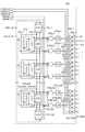
図4は実施形態1における走査線駆動回路21の構成図であり、図5は図4の各構成要素の構成図である。 4 is a configuration diagram of the scanning
走査線駆動回路21は、順次選択回路71と、順次選択回路71の出力段に接続されるレベルシフタ回路81、レベルシフタ回路81の出力段と走査線21に接続される出力回路82とから構成される。 The scanning
図4の破線71は双方向シフトレジスタを用いた順次選択回路であり、電圧VD−VSレベルで駆動される。ここでVD=8V、VS=0Vとする。 A
順次選択回路71は、単位回路としてクロック制御回路(CCC:Clock Control Circuit)72と、クロック生成回路(CGC:Clock Generate Circuit)73と、ラッチ回路74と、双方向転送回路75と、NAND回路76とで構成される。 The
クロック制御回路72は、図4及び図5(A)に示すように、クロック信号端子31aからクロック信号VCLKを入力すると共に、双方向転送回路75の信号CT1、CT2に基づいてクロック生成回路73にクロック信号を供給するものである。すなわち、信号CT1、CT2のいずれかがHighの時にクロック信号を通過させ、両方ともLowの時にはクロック信号を遮断し、固定電位VS又はVDレベルを出力させる。これにより、必要な段にのみクロックを供給し、他は遮断することでクロック信号VCLKの負荷を低減することができる。本実施形態1ではn=奇数の段ではVS、n=偶数の段ではVDレベルを用いる。この構成により、信号の転送が生じている段にのみクロック信号を供給することでクロック信号線77の容量を低減し、遅延による誤動作を防止するとともに消費電流を低減する。なお、クロック制御回路72はクロック信号線77の負荷が問題にならない場合は省略可能である。 As shown in FIGS. 4 and 5A, the
次にクロック生成回路73は、図4及び図5(B)に示すように、クロック制御回路72から出力された単極のクロック信号VCLKを入力し、位相ズレのない両極クロック信号を生成し、ラッチ回路74に出力する回路である。この構成により、出力される両極クロック信号間の位相ズレによるラッチ回路74の誤動作を防止できる。なお、クロック生成回路73はクロック信号の位相ズレが問題にならない場合はクロック信号VLCKの逆極性信号を入力することで省略可能である。 Next, as shown in FIG. 4 and FIG. 5B, the
ラッチ回路74は、図4及び図5(C)に示すように、スタートパルス信号端子31bで入力されたスタートパルス信号VSPを、クロック信号VCLKからクロック生成回路73で生成されたクロック信号によって、ラッチもしくは順次転送する。すなわち、ラッチ回路74は、クロック信号CL=High、反転クロック信号CX=Lowの時にはスタートパルス信号VSPを転送し、クロック信号CL=Low、反転クロック信号CX=Highの時にはラッチ動作を行う。また、初期化信号INITがHighの時には強制的にLow出力を行い、リセットを行う。 4 and 5C, the
また、双方向転送回路75は、図4及び図5(D)に示すように、転送方向制御信号VDIR=HIGH、転送方向反転制御信号VDIRX=LOWの時にはn=1→2→3・・・の順に転送する正方向転送、転送方向制御信号VDIR=LOW、転送方向反転制御信号VDIRX=HIGHの時にはn=480→479→478・・・の順に転送する逆方向転送を行う。なお、双方向転送が不要な場合は、双方向転送回路75は省略可能である。 As shown in FIGS. 4 and 5D, when the transfer direction control signal VDIR = HIGH and the transfer direction inversion control signal VDIRX = LOW, the
NAND回路76は、ラッチ回路74の前後段の出力信号と、イネーブル信号端子VENBからのイネーブル信号を入力し、順次選択回路71の出力信号として出力する。具体的には、ラッチ回路74からの出力はNAND回路76に入力され、イネーブル信号端子31cから供給されたイネーブル信号VENBがHIGH(=VD)のタイミングに選択された段のみNAND回路76はLOW(=VSレベル)を出力し、他段はHigh(=VD)レベルを出力する。 The NAND circuit 76 inputs the output signal before and after the
このVD−VSレベル信号はレベルシフタ回路81によってVH−VLLレベルに変換され、出力回路82のnチャネル型トランジスタ83、pチャネル型トランジスタ84に入力される。 The VD-VS level signal is converted to the VH-VLL level by the
図5(E)はレベルシフタ回路81の構成図であり、いわゆるフリップ・フロップタイプのレベルシフタを2段直列に配置することで、VD−VSレベルの信号をVH−VLL信号に変換する。NAND回路76からの出力信号がLow(=VS)、すなわち選択状態であれば、pチャネル型トランジスタ84によって走査線13にはVH電位が書き込まれる。これにより、画素スイッチング素子43のトランジスタのゲート電極に選択電位としてVHの電位が供給され、画素スイッチング素子43を電気的に低インピーダンスにする。また、NAND回路76からの出力信号がHigh(=VH)の場合はnチャネル型トランジスタ85、86によって極性信号POLがHIGHの場合は電位VLM、極性反転信号POLXがHIGHの場合は電位VLLがそれぞれ選択され、nチャネル型トランジスタ83によって走査線13に書き込まれる。これにより、画素スイッチング素子43のトランジスタのゲート電極に非選択電位としてVH−VLL/VLMの電位が供給され、画素スイッチング素子43を電気的に高インピーダンスにする。 FIG. 5E is a configuration diagram of the
よって最終的に走査線13に電位VH−VLL/VLMレベルの信号が加えられる。ここで、VH=10V、VLM=−1V、VLL=−5Vとする。なお、本実施形態1ではこのように電位VLLと電位VLMを切り替えるのに極性信号POLを用いて走査線駆動回路21内の各段でスイッチを設けているが、出力回路82を通常の相補型インバータ構成とし、nチャネル型トランジスタに繋がる電源電位線を−4.5V〜−0.5VレベルでAC駆動してもよい。この場合、位相はコモン電位信号VCOMと一致させる。また、反転タイミングでは走査線をフローティングとし、コモン電極との結合容量で反転させてもよい。 Therefore, a signal having a potential VH−VLL / VLM level is finally applied to the
図6はデータ線駆動回路23の構成例である。信号入力端子31から供給される映像信号VIDEO1〜320は、それぞれ選択信号線91の数に対応して設けられた伝送ゲートスイッチ92にブロック毎に接続される。そして、映像信号VIDEOは、選択信号SEL1〜6で選択された各ブロック内の伝送ゲートスイッチ92によって、伝送ゲートスイッチ92に対応するデータ線15に書き込まれる。いわゆる1:6のマルチプレクサによる部分ドライバ方式である。選択信号SEL1〜6はVH−VLLレベルであり、図6の93は選択信号SEL1〜6の逆極性信号を生成するインバータ回路であって、電源はVH−VLLレベルである。また、映像信号VIDEOは、0.5〜4.5Vの電位振幅である。 FIG. 6 shows a configuration example of the data line driving
このような構成により、選択信号SEL1がHigh(=VH)、他の選択信号SEL2〜6がLow(=VLL)になると、映像信号VIDEO1とブロック内のデータ線15−1が短絡し、同ブロック内の他のデータ線15−2〜6は絶縁される。次に選択信号SEL2がHigh(=VH)、他の選択信号SEL信号1、選択信号SEL3〜6がLow(=VLL)になると、映像信号VIDEO2とデータ線15−2が短絡し、他のデータ線15−1、15−3〜6は絶縁される。このように1走査線選択期間内で選択信号SEL1〜6を順次Highにすることで映像信号VIDEO1信号をデータ線15−1〜6に分配することができる。 With this configuration, when the selection signal SEL1 is High (= VH) and the other selection signals SEL2 to SEL2 are Low (= VLL), the video signal VIDEO1 and the data line 15-1 in the block are short-circuited, and the same block The other data lines 15-2 to 6 are isolated. Next, when the selection signal SEL2 is High (= VH), the other selection
図7はデータ線プリチャージ回路25の構成例である。各データ線15は伝送ゲートスイッチ95を介してコモン電位端子からコモン電位VCOMが供給されるコモン電位線96に接続される。そして、各伝送ゲートスイッチ95のゲートにはプリチャージ信号供給端子31eからプリチャージ信号PRCが供給されるプリチャージ信号線96が共通接続される。そして、プリチャージ信号PRCによって一斉に各データ線15にコモン電位VCOMが書き込まれる。これにより、データ線書き込み時の負荷が軽減され、確実に書き込みが可能となる。ここではコモン電位VCOMとしたが、書き込み能力に応じ、適当な電位を与えても良い。例えば中間グレーレベル電位であれば、2.5V電位を与えればよい。なお、書き込み時間が十分であるならデータ線プリチャージ回路25は省略化である。また、データ線プリチャージ回路25を省略してデータ線駆動回路23を通じてプリチャージを行う方法もある。すなわち、プリチャージ信号PRC選択のタイミングで選択信号SEL1〜6を全選択し、映像信号1〜320にコモン電位信号VCOMの電位又は相応の電位を供給すればよい。 FIG. 7 shows a configuration example of the data line
ここで、本実施形態1の液晶表示装置の画素配列は縦モザイク構造を成している。すなわち、対向基板12の画素電極45に対応する領域には、前述したブロック内毎に、図中左より赤(R)、緑(G)、青(B)、赤(R)、緑(G)、青(B)と繰り返すように、カラーフィルタが設けられている。よって、データ線15−1,4,7,…,1918に繋がる画素電極402−n−1,4,7,…,1918と対向する対向基板12上の色材は全て赤(R)である。すなわち選択信号SEL1およびSEL4信号が選択されるタイミングによって書き込まれる映像信号は全て赤(R)である。同様に選択信号SEL2およびSEL5信号が選択されるタイミングによって書き込まれる映像信号は全て緑(G)であり、選択信号SEL3およびSEL6が選択されるタイミングによって書き込まれる映像信号は全て青(B)である。 Here, the pixel arrangement of the liquid crystal display device according to the first embodiment has a vertical mosaic structure. That is, in the area corresponding to the
次に、図8は信号入力端子31を通じて入力される各制御信号のタイミングを示すタイミングチャートである。図8(A)は走査線駆動回路21の制御信号であるスタートパルス信号VSP、クロック信号VCLK、イネーブル信号VENBおよびコモン電位入力端子32から入力されるコモン電位信号VCOM、及び走査線13−1、13−2に走査線駆動回路21から出力される信号を示すチャートである。スタートパルス信号VSPは1フィールド期間、本実施形態1ではリフレッシュレート60Hzであるので16.67ミリ秒の周期で入力されるスタートパルス信号である。クロック信号VCLKは走査期間、すなわち本実施形態1では34.72マイクロ秒周期で反転するクロック信号である。そして、イネーブル信号VENBは走査期間周期のパルス波であり、31.25マイクロ秒のパルス長である。極性信号POLはクロック信号VCLKと同周期信号であって、クロック信号VCLKとは17.36マイクロ秒だけ位相がずれた信号である。図示しないが、極性反転信号POLXは極性信号POLと同周波数・同振幅で極性が反転した信号である。スタートパルス信号VSP、クロック信号VCLK、イネーブル信号VENBはいずれもVS−VDレベルの信号であって、極性信号POL、極性反転信号POLXはVLL−VHレベルの信号である。また、転送方向制御信号VDIRはVDレベルに固定、転送方向反転制御信号VDIRXと初期信号INITはVSレベルに固定となる。このような信号を走査線駆動回路21に入力することで、走査線13−nは各走査周期でいずれか1本が31.25マイクロ秒程度の間、Highとなり、n=1,2,3...の順に34.72マイクロ秒間隔で選択されていく(転送方向制御信号VDIR=VD,転送方向反転制御信号VDIRX=VSの場合)。非選択期間は極性信号POLに同期してVLL−VLMレベル間で反転駆動される。コモン電位信号VCOMは極性信号POLと同じ周波数・位相の矩形波であって、LOW側電位が0.5V、High側電位が4.5Vである。 Next, FIG. 8 is a timing chart showing the timing of each control signal input through the
図8(B)は図8(A)の期間Bの間のデータ線駆動回路23における選択信号SEL1〜6、プリチャージ信号PRC及び映像信号VIDEO1〜320のタイミングチャートである。なお、この図8(B)でVIDEO(W)とは全面白表示(ノーマリー・ブラックモードなら黒表示)時のVIDEO1〜320に入力される映像信号、VIDEO(B)とは全面黒表示(ノーマリー・ブラックモードなら白表示)時のVIDEO1〜320に入力される映像信号である。点線は特に規定しない、あるいはハイインピーダンス状態を示す。このように、1走査期間でプリチャージ信号PRC→選択信号SEL1→選択信号SEL5→選択信号SEL3→選択信号SEL4→選択信号SEL2→選択信号SEL6の順に選択される。対応する色の順序で言うと、R→G→B→R→G→Bである。選択信号SEL1〜6の選択期間は各3.16マイクロ秒である。ここで選択信号SEL1、選択信号SEL5、選択信号SEL3の選択期間が第1の選択期間であり、SEL4、SEL2、SEL6の選択期間が第2の選択期間と定義付けられる。各選択期間の間には選択信号SEL1〜6およびプリチャージ信号PRCが全て非選択になる期間があり、選択信号SEL3選択期間と選択信号SEL4選択期間の間の非選択期間(第1の非選択期間)のみがt2=3.16マイクロ秒、それ以外の非選択期間(第2の非選択期間)がt1=1.58マイクロ秒である。コモン電位信号VCOMは選択信号SEL3の選択期間と選択信号SEL4の選択期間との間の第1の非選択期間中に反転する。このようにコモン電位信号VCOMが反転する時の非選択期間だけを長くとるのは、コモン電位信号VCOMの反転開始からコモン電位信号VCOMが緩和するのに十分な時間、全てのデータ線をハイインピーダンス状態にする必要があるためである。かといって、t1=3.16マイクロ秒とすると選択信号SEL1〜6の選択期間の幅が2.63マイクロ秒となってしまい、書き込みが不十分となる恐れがある。なお、選択信号SEL1〜6とプリチャージ信号PRCはVH−VLLレベル信号(−5〜10V電位振幅)であり、映像信号VIDEO1〜320は0.5〜4.5V電位振幅である。 FIG. 8B is a timing chart of the selection signals SEL1 to SEL1, the precharge signal PRC, and the video signals VIDEO1 to 320 in the data
ここで全画素に黒電位(VIDEO(B))を書き込むことを想定し、走査期間を通して各タイミングでの電位について考える。コモン電位信号VCOMは最初0.5Vとする。まず、プリチャージ信号PRCが選択されてデータ線プリチャージ回路25が動作し、全データ線15は0.5Vに書き込まれる。次にイネーブル信号VENBがONし、1本の特定の走査線13が選択電位(=VH)になる。残りの走査線479本は非選択電位(=VLL)である。ここで選択信号SEL1が選択され、データ線15−1、7、…1915に4.5V電位が書き込まれる。ここでデータ線15−1、7、…1915は左から走査線方向に数えて奇数番目の赤色表示に対応した画素に接続されているので、以下便宜上、Roddラインと呼ぶ。同様にデータ線15−2、8、…1916をGoddライン、以下データ線15−3、9、…1917をBoddライン、データ線15−4、10、…1918をRevenライン、データ線15−5、11、…1919をGevenライン、データ線15−6、11、…1920をBevenラインと呼ぶ。次に選択信号SEL4が選択されてGevenライン、選択信号SEL3が選択されてBoddラインに4.5Vが書き込まれる。この時点でRoddライン、Gevenライン、Boddラインの各ラインに接続された画素電極45−n−1,3,5…は0.5Vから4.5Vへ書き込みが行われている途中である。一方、Revenライン、Goddライン、Bevenラインの各ライン及び接続された画素電極45−n−2,4,6…はプリチャージ電位のまま、0.5V電位にある。 Here, it is assumed that a black potential (VIDEO (B)) is written in all pixels, and the potential at each timing is considered throughout the scanning period. The common potential signal VCOM is initially set to 0.5V. First, the precharge signal PRC is selected, the data line
次にコモン反転タイミングになり、コモン電位信号VCOMは0.5Vから4.5Vへ反転し、同時に極性信号POL、極性反転信号POLXも反転するために各走査線13−nの非保持電位もVLLからVLMに反転する。1マイクロ秒程度の緩和時間の後、コモン電位信号VCOMは所定の電位に達するが、この際、全データ線15は接続されている伝送ゲートスイッチ92−n、95−nがハイインピーダンス状態であるため、容量結合で電位が引き上げられる。データ線15の容量を走査線13−nとの交差容量C1、容量線17−nとの交差容量及び対向電極との容量C2、伝送ゲートゲート92−n,95−nの寄生容量、モジュール筐体のGNDやパネル内の電源との寄生容量などのその他の容量C3の3つに分解すると、データ線の容量結合による電位変動幅ΔVは、ΔV=479÷480*C1*(VLM−VLL)÷(C1+C2+C3)+C2*(4.5−0.5)÷(C1+C2+C3)となる。VLM=−1V、VLL=−4Vであるから、ΔV=4*(479÷480*C1+C2)÷(C1+C2+C3)となる。なお、画素電極45はいずれもフローティング状態であるか、データ線15に短絡されているかであるので画素電極45との容量はここでは考慮する必要はない。本実施形態1では対角4インチの液晶ディスプレイであり、C1〜C3は電界シミュレーション等の結果から、C1=2.5pF、C2=16.3pF、C3=0.08pFとなる。従って、ΔV=3.98Vであって、Roddライン、Gevenライン、Boddラインの各データラインは8.48V、Revenライン、Goddライン、Bevenラインの各データラインは4.48Vとなる。また、各画素電極45の容量はほぼ100%が容量線、対向電極、走査線、データ線との容量であるから、ほぼ容量結合で4V電位が変動し、画素電極45−n−1,3,5…は4.5〜8.5Vの間、画素電極45−n−2,4,6…は4.5V電位となる。 Next, at the common inversion timing, the common potential signal VCOM is inverted from 0.5 V to 4.5 V. At the same time, the polarity signal POL and the polarity inversion signal POLX are also inverted, so the non-holding potential of each scanning line 13-n is also VLL. From VLM to VLM. After the relaxation time of about 1 microsecond, the common potential signal VCOM reaches a predetermined potential. At this time, the transmission gate switches 92-n and 95-n to which all the data lines 15 are connected are in a high impedance state. Therefore, the potential is raised by capacitive coupling. The capacitance of the
この後、選択信号SEL4→選択信号SEL2→選択信号SEL6の順に選択され、Revenライン、Goddライン、Bevenラインはそれぞれ0.5V電位を書き込まれる。選択信号SEL6が非選択になった後、イネーブル信号VENBがOFF(=VS)して走査線13−nがVLM電位になるまでの間(図7(B)のt3期間=3.16マイクロ秒)に最終的にデータ線15の電位が画素電極45に書き込まれ、画素電極45−n−1,3,5…はほぼ8.48V、画素電極45−n−2,4,6…はほぼ0.5Vとなる。なお、ここでは画素スイッチング素子43のフィードスルーなどは無視している。 Thereafter, the selection signal SEL4, the selection signal SEL2, and the selection signal SEL6 are selected in this order, and the Reven line, the Godd line, and the Even line are each written with a potential of 0.5V. After the selection signal SEL6 is deselected, the enable signal VENB is turned OFF (= VS) and the scanning line 13-n becomes the VLM potential (t3 period in FIG. 7B = 3.16 microseconds). ) Is finally written into the
次の走査線選択期間(走査線13−n+1がVHになる期間)ではコモン電位信号VCOMは4.5Vから始まり、同様に途中で反転して0.5Vになる。この際の動作は容量結合での変動幅の正負が逆になる他は全く上記と同様であって、最終的にイネーブルVENB信号がOFFする時点では画素電極45−n+1−1,3,5…はほぼ−3.48V、画素電極45−n+1−2,4,6…はほぼ+4.5Vとなる。以上を480走査線分繰り返して1フィールド期間の書き込みは完了する。 In the next scanning line selection period (period in which scanning line 13-
このタイミングでの各画素の液晶素子に印加される電圧(=画素電極電位−コモン電極の電位)は図9に示すようになる。なお、ここで+はコモン電極より高い電位をプラス極性、−はコモン電極より低い電位をマイナス極性であることを示しており、1フィールド期間後では全ての画素で正負が逆になる。これはすなわち、いわゆるドット反転駆動となっており、フリッカーが視認しにくい構成となっている。 The voltage applied to the liquid crystal element of each pixel at this timing (= pixel electrode potential−common electrode potential) is as shown in FIG. Here, + indicates that the potential higher than that of the common electrode is positive polarity, and − indicates that the potential lower than that of the common electrode is negative polarity, and after one field period, the positive / negative is reversed in all pixels. In other words, this is so-called dot inversion driving, and flicker is difficult to visually recognize.
以上のように、各データ線15は約−3.5V〜+8.5V程度の電位振幅となり、この時に画素スイッチング素子43で確実に画素電極45に書き込めるように走査線駆動回路21のVH、VL電位は設定されてなくてはならない。画素スイッチング素子43のトランジスタの閾値をVthとすると、VH≧8.5V+Vthであり、本実施形態1ではVth=1.0VであるのでVHは10Vと設定した。また、データ線駆動回路23の伝送ゲートスイッチ92−nおよびデータ線プリチャージ回路25の伝送ゲートスイッチ95−nを制御している電源電圧もデータ線15からのリークを避けるために各データ線15の電位振幅である約−3.5V〜+8.5Vより大きな電位振幅でなくてはならず、VH=10V、VLL=−5Vとした。なお、本実施形態1では走査線駆動回路21のVH、VLLおよびデータ線駆動回路23のVH、VLLは入力端子、電源IC削減のため共通としたが、これらは別の電位としてもよい。この場合、上記の条件からわかるとおり、走査線駆動回路21のVHはデータ線駆動回路23のVHより高くとるべきである。 As described above, each
参考に対比例として、図10に従来のデータ線駆動回路に与えていた制御信号のタイミングチャートを示す。コモン電位信号VCOMと極性信号POLは、クロック信号VCLKと位相のずれのない同周期の信号である。選択信号SELは、SEL1→SEL2→SEL3→・・・→SEL6と順次供給される。この時のあるタイミングでの各画素の液晶素子に印加される電圧は図11に示すようになる。これはいわゆるゲート反転駆動(あるいはロウ(LOW)反転駆動、1H反転駆動という)であって、従来コモン反転タイミングは全ての走査線が閉じているタイミング(=イネーブル信号VENBがOFFのタイミング)であったので、このようにゲート反転駆動しかできなかったのである。このため、画素フィードスルーや画素スイッチング素子のトランジスタのリークに起因するフリッカーが見えやすく、画質が劣るとともにフレーム周波数を低下させることが難しかったが、本実施形態1の駆動方法によりこの問題を解決できる。 For reference, FIG. 10 shows a timing chart of control signals applied to a conventional data line driving circuit. The common potential signal VCOM and the polarity signal POL are signals having the same period with no phase shift from the clock signal VCLK. The selection signal SEL is sequentially supplied in the order of SEL1, SEL2, SEL3,. The voltage applied to the liquid crystal element of each pixel at a certain timing at this time is as shown in FIG. This is so-called gate inversion drive (or low (LOW) inversion drive, 1H inversion drive), and the conventional common inversion timing is the timing at which all scanning lines are closed (= the timing when the enable signal VENB is OFF). Therefore, only gate inversion drive was possible in this way. For this reason, flicker caused by pixel feedthrough or transistor leakage of the pixel switching element is easy to see, and the image quality is inferior and it is difficult to lower the frame frequency. However, the driving method of the first embodiment can solve this problem. .
さて、本実施形態1の駆動方法では第1の選択期間に書き込んだ画素はデータ線15の外部容量および選択された走査線13の容量(C3+C1÷480)に起因する電圧低下が発生する。しかし、これは正負両極性で同様に起こるのでDCバイアスとしては0であり、ある画素に着目するとフレーム間での液晶の透過率に差異はなく、液晶素子の信頼性劣化やフリッカー要因とはならない。厳密には画素ピッチで微妙な濃淡差となるが、画素電圧の差異は20mVであって、せいぜい64階調表示での1階調分にしか相当せず、視認できないレベルである。このように、本実施形態1の駆動方法を用いる際はC3+C1÷nがC1+C2+C3に比べ十分小さい必要がある。ここでC1はデータ線における全走査線との交差容量、C2はデータ線とコモン電極(対向基板のコモン電極でよいですか?)との容量、C3はデータ線とそれ以外の容量、nは走査線数である。より具体的にはC3+C1÷nがC1+C2+C3の0.5%以下であれば階調のズレは64分の1階調以下であって視認できなくなる。具体的に実現方法を述べると、コモン反転タイミングでデータ線を映像信号やプリチャージ信号からハイインピーダンスで絶縁するスイッチング回路、本実施形態1で言うと伝送ゲートスイッチ92−n、95−nはアクティブマトリクス回路形成基板内に作りこむことが望ましい。外部ICにこの役割を持たせた場合、実装部品や途中配線での寄生容量が大きく、容量C3が大きくなってしまうためである。従って、本実施形態1は特にポリシリコンTFTを用いた液晶表示装置で有効であると言える。また、走査線数nが大きいほど好ましいから高精細な液晶表示装置に向く技術でもある。 In the driving method of the first embodiment, a voltage drop caused by the external capacitance of the
また、上記の条件を満たせない場合、すなわち前記C3+C1÷nが小さく出来ない場合は第1の選択期間への書き込みの映像信号電圧−コモン電圧の電位振幅を同じ階調表示をさせる第2の選択期間への書き込みの映像信号電圧−コモン電圧の電位振幅に比べ、1+2*(C3+C1÷n)÷(C1+C2+C3)倍すればよい。本実施形態1でいうとRoddライン、Gevenライン、Boddラインのデータ線への書き込み時、すなわち選択信号SEL1、選択信号SEL5、選択信号SEL3の選択時の黒表示映像信号を4.52/0.48Vとし、Revenライン、Goddライン、Bevenラインのデータ線への書き込み時、すなわち選択信号SEL4、選択信号SEL2、選択信号SEL6の選択時の黒表示映像信号を4.50/0.50Vとすればよいことになる。 When the above condition cannot be satisfied, that is, when C3 + C1 ÷ n cannot be reduced, the second selection for displaying the same gradation display of the potential amplitude of the video signal voltage to be written to the common selection voltage during the first selection period. It may be multiplied by 1 + 2 * (C3 + C1 ÷ n) ÷ (C1 + C2 + C3) as compared with the potential amplitude of the video signal voltage for writing to the period−common voltage. In the first embodiment, the black display video signal at the time of writing to the data lines of the Rodd line, the Geven line, and the Bodd line, that is, the selection signal SEL1, the selection signal SEL5, and the selection signal SEL3 is 4.52 / 0. 48V, and the black display video signal is 4.50 / 0.50V when writing to the data line of the Reven line, Godd line, and Even line, that is, when the selection signal SEL4, the selection signal SEL2, and the selection signal SEL6 are selected. It will be good.
このように構成された液晶表示装置では、従来のものより低フリッカーであって映像品位が高く、またフレームレートを落としてもフリッカーが見えずらいため、低消費電力化が容易である。このような液晶表示装置を用いた電子機器では映像品位が向上し、より低消費電力で駆動することができるためにバッテリー持続性等に優れる。ここでいう電子機器とはモニター、TV、ノートパソコン、PDA、デジタルカメラ、ビデオカメラ、携帯電話、携帯フォトビューワー、携帯ビデオプレイヤー、携帯DVDプレイヤー、携帯オーディオプレイヤーなどである。
[実施形態2]In the liquid crystal display device configured in this manner, the flicker is lower than that of the conventional one, the image quality is high, and even if the frame rate is lowered, it is difficult to see the flicker. An electronic apparatus using such a liquid crystal display device has improved image quality and can be driven with lower power consumption, and thus has excellent battery sustainability and the like. Examples of the electronic device include a monitor, a TV, a notebook computer, a PDA, a digital camera, a video camera, a mobile phone, a mobile photo viewer, a mobile video player, a mobile DVD player, and a mobile audio player.
[Embodiment 2]
図12は実施形態2を実現するデータ線駆動回路123の構成図である。実施形態2では、単位ブロックをデータ線3本毎とし、それに応じて3つの選択信号SEL1〜3を用いて制御するものである。信号入力端子31から供給される映像信号VIDEO1〜640信号は選択信号SEL1〜3によって伝送ゲートスイッチ192−1〜1920で分配され、データ線15−1〜1920に書き込まれる、いわゆる1:3のマルチプレクサによる部分ドライバ方式である。具体的には、映像信号VIDEO1は伝送ゲートスイッチ192−1〜3、映像信号VIDEO2は伝送ゲートスイッチ192−4〜6というように接続される。選択信号SEL1は伝送ゲートスイッチ192−3、192−6・・・に接続され、選択信号SEL2は伝送ゲートスイッチ192−2、192−5・・・に接続され、選択信号SEL3は伝送ゲートスイッチ192−1、192−4・・・に接続される。193−1〜3は極性を反転させるインバータ回路であって、電源はVH−VLLレベルである。 FIG. 12 is a configuration diagram of the data line driving
その他、液晶表示装置の構成、アクティブマトリクス基板の構成、走査線駆動回路の構成、データ線プリチャージ回路の構成は実施形態1と同様であるので説明を省略する。 In addition, since the configuration of the liquid crystal display device, the configuration of the active matrix substrate, the configuration of the scanning line driving circuit, and the configuration of the data line precharge circuit are the same as those in the first embodiment, the description thereof is omitted.
図13は実施形態2における信号入力端子31を通じて入力される制御信号のタイミングを示すタイミングチャートである。図13(A)は走査線駆動回路21の制御信号であるスタートパルス信号VSP、クロック信号VCLK、イネーブル信号VENBおよびコモン電位入力端子31dから入力されるコモン電位信号VCOM、及び走査線13−1、13−2に走査線駆動回路21から出力される信号を示すチャートである。各信号のタイミング及び動作は実施形態1の図8(A)と同じであるので説明は省略する。 FIG. 13 is a timing chart showing the timing of the control signal input through the
図13(B)は図13(A)の期間Bの間のデータ線駆動回路123における選択信号SEL1〜3、プリチャージ信号PRC及び映像信号VIDEO1〜640のタイミングチャートである。なお、この図13(B)でVIDEO(W)とは全面白表示(ノーマリー・ブラックモードなら黒表示)時のVIDEO1〜640に入力される映像信号、VIDEO(B)とは全面黒表示(ノーマリー・ブラックモードなら白表示)時のVIDEO1〜640に入力される映像信号である。点線は特に規定しない、あるいはハイインピーダンス状態を示す。このように、1走査期間でプリチャージ信号PRC→選択信号SEL1→選択信号SEL2→選択信号SEL3の順に選択される。対応する色の順序で言うと、R→G→Bである。選択信号SEL1〜3の選択期間は4.74マイクロ秒である。ここで選択信号SEL1の選択期間が第1の選択期間であり、選択信号SEL2、選択信号SEL3の選択期間が第2の選択期間と定義付けられる。各選択期間の間には選択信号SEL1〜3およびプリチャージ信号PRCが全て非選択になる期間があり、選択信号SEL1の選択期間と選択信号SEL2の選択期間との間の非選択期間(第1の非選択期間)がt2=6.32マイクロ秒、選択信号SEL2の選択期間と選択信号SEL3の選択期間との間の非選択期間(第2の非選択期間)がt1=3.16マイクロ秒である。コモン電位信号VCOMは選択信号SEL1の選択期間と選択信号SEL2の選択期間との間の非選択期間中に反転する。t2>t1である理由は実施形態1に同じである。 FIG. 13B is a timing chart of the selection signals SEL1 to SEL3, the precharge signal PRC, and the video signals VIDEO1 to 640 in the data
入力信号レベルはクロック信号VCLK、スタートパルス信号VSP、イネーブル信号VENBがVD−VSレベル信号(0〜8V電位振幅)、選択信号SEL1〜3、プリチャージ信号PRC、極性信号POL、極性反転信号POLXはVH−VLLレベル信号(−5〜10V電位振幅)、映像信号VIDEO1〜640およびコモン電位信号VCOMは0.5〜4.5V電位振幅の信号である。 The input signal level is the clock signal VCLK, the start pulse signal VSP, the enable signal VENB is the VD-VS level signal (0 to 8 V potential amplitude), the selection signals SEL1 to SEL3, the precharge signal PRC, the polarity signal POL, and the polarity inversion signal POLX are The VH-VLL level signal (-5 to 10 V potential amplitude), the video signals
このようなタイミングの駆動を行うと、あるタイミングでの各画素の液晶素子に印加される電圧(=画素電極電位−コモン電極の電位)は図14に示すようになる。なお、ここで+はコモン電極より高い電位をプラス極性、−はコモン電極より低い電位をマイナス極性であることを示しており、1フィールド期間後では全ての画素で正負が逆になる。実施形態1の図9に示すように完全なドット反転にはなっていないが、同一走査線上に極性の異なる画素が混在するため、図11に示す従来のゲート反転駆動よりはフリッカーに対して強い構成となっている。 When driving at such timing, the voltage (= pixel electrode potential−common electrode potential) applied to the liquid crystal element of each pixel at a certain timing is as shown in FIG. Here, + indicates that the potential higher than that of the common electrode is positive polarity, and − indicates that the potential lower than that of the common electrode is negative polarity, and after one field period, the positive / negative is reversed in all pixels. Although the dot inversion is not complete as shown in FIG. 9 of the first embodiment, pixels having different polarities coexist on the same scanning line, so that it is more resistant to flicker than the conventional gate inversion driving shown in FIG. It has a configuration.
なお、本実施形態2では選択信号SEL1の選択期間と選択信号SEL2の選択期間との間でコモン反転を行っている。これは比較的人間の目に敏感な赤の画素と緑の画素の極性を逆にした方が、選択信号SEL2の選択期間と選択信号SEL3の選択期間との間でコモン反転を行って赤の画素と緑の画素の極性が同じであるよりもフリッカーが見えにくいためである。 In the second embodiment, common inversion is performed between the selection period of the selection signal SEL1 and the selection period of the selection signal SEL2. This is because when the polarity of the red pixel and the green pixel which are relatively sensitive to human eyes are reversed, the common inversion is performed between the selection period of the selection signal SEL2 and the selection period of the selection signal SEL3. This is because the flicker is less visible than the polarities of the pixel and the green pixel are the same.
また、同様に1:3のマルチプレクサ構成であっても、データ線駆動回路の構成を図15に示す変形例のようにして図13に示す信号を入力してもよい。すなわち、データ線駆動回路223の映像信号VIDEO1は伝送ゲートスイッチ292−1、292−4、292−7に接続され、映像信号VIDEO2は伝送ゲートスイッチ292−2、292−5、292−8に接続され、映像信号VIDEO3は伝送ゲートスイッチ292−3、292−6、292−9に接続され、これらを単位ブロックとして各映像信号VIDEOは対応する伝送ゲートスイッチ292に接続される。そして、選択信号SEL1は伝送ゲートスイッチ292−7〜9、選択信号SEL2は伝送ゲートスイッチ292−4〜6、選択信号SEL3は伝送ゲートスイッチ292−1〜3を単位ブロックとして接続される。293−1〜3は極性を反転させるインバータ回路であって、電源はVH−VLLレベルである。この構成によれば、あるタイミングでの各画素の液晶素子に印加される電圧(=画素電極電位−コモン電極の電位)は図16に示すようになる。これはドット反転ではないが、同一走査線上で各色の画素同士は極性が反転しており、ドット反転に近いレベルでフリッカーが視認しにくい。 Similarly, even in the case of a 1: 3 multiplexer configuration, the signal shown in FIG. 13 may be inputted as in the modification shown in FIG. 15 in the configuration of the data line driving circuit. That is, the video signal VIDEO1 of the data line driving
無論、同様に1:2駆動、1:4駆動などを用いても構わない。いずれの場合でも従来のゲート反転駆動よりフリッカーの見えにくい反転駆動が実現可能である。
[実施形態3]Of course, similarly, 1: 2 drive, 1: 4 drive, or the like may be used. In either case, inversion driving in which flicker is less visible than conventional gate inversion driving can be realized.
[Embodiment 3]
図17は実施形態3を実現するデータ線駆動回路323の構成図である。いわゆるアナログ点順次型のデータ駆動回路構成であって、クロック制御回路(CCC:Clock Control Circuit)回路372、クロック生成回路(CGC:Clock Generate Circuit)373、ラッチ回路374、双方向転送回路375からなる双方向シフトレジスタを用いた順次選択回路を構成している。この順次選択回路は実施形態1で説明した走査線駆動回路と同様であって、各回路の具体的構成も図5(A)〜(D)で示した通りである。 FIG. 17 is a configuration diagram of the data line driving
ただし、一対のNAND回路376a、376bが各段に配置され、NAND回路376aにはイネーブル信号HENB1が供給され、NAND回路376bにはイネーブル信号HENB2が供給される。NAND回路376a、376bに応じて一対のレベルシフタ回路377a、377bが配置されている。この動作も実施形態1で説明したとおりであるので省略する。レベルシフタ回路377a、377bの具体的回路構成も図5(E)で示した通りである。 However, a pair of
レベルシフタ回路377aには、データ線15−1、15−3、15−5に対応した伝送ゲートスイッチ392−1、392−3、392−5に接続される。また、レベルシフタ回路377bには、データ線15−2、15−4、15−6に対応した伝送ゲートスイッチ392−2、392−4、392−6に接続される。そして、赤の映像信号VIDEO−Rは伝送ゲートスイッチ392−1、392−4に接続され、緑の映像信号VIDEO−Gは伝送ゲートスイッチ392−2、392−5に接続され、青の映像信号VIDEO−Bは伝送ゲートスイッチ392−3、392−6に接続される。これらデータ線6本毎を単位ブロックとして順次接続される。 The
この構成により、例えばラッチ回路374−1が選択された時にイネーブル信号HENB1がHIGHになればNAND回路376a−1、レベルシフタ回路377a−1を介して伝送ゲートスイッチ392−1、392−3、392−5がONとなる。そして奇数のデータ線のうちデータ線15−1には赤の映像信号VIDEO−Rが供給され、データ線15−3には青の映像信号VIDEO−Bが供給され、データ線15−5には緑の映像信号VIDEO−Gが供給される。また、ラッチ回路374−1が選択された時にイネーブル信号HENB2がHIGHになればNAND回路376b−1、レベルシフタ回路377b−1を介して伝送ゲートスイッチ392−2、392−4、392−6がONとなる。そして偶数のデータ線のうちデータ線15−2には緑の映像信号VIDEO−Gが供給され、データ線15−4には赤の映像信号VIDEO−Rが供給され、データ線15−6には青の映像信号VIDEO−Bが供給される。 With this configuration, for example, if the enable signal HENB1 becomes HIGH when the latch circuit 374-1 is selected, the transmission gate switches 392-1, 392-3, and 392-through the
また、液晶表示装置の構成、アクティブマトリクス基板の構成、走査線駆動回路の構成、データ線プリチャージ回路の構成は実施形態1と同様であるので説明を省略する。 The configuration of the liquid crystal display device, the configuration of the active matrix substrate, the configuration of the scanning line driving circuit, and the configuration of the data line precharge circuit are the same as those in the first embodiment, and thus description thereof is omitted.
図18は実施形態3における信号入力端子31を通じて入力される制御信号のタイミングを示すタイミングチャートである。図18(A)は走査線駆動回路21の制御信号であるスタートパルス信号VSP、クロック信号VCLK、イネーブル信号VENBおよびコモン電位入力端子31dから入力されるコモン電位信号VCOM、及び走査線13−1、13−2に走査線駆動回路21から出力される信号を示すチャートである。詳細は実施形態1の図8(A)と同じであるので説明は省略する。 FIG. 18 is a timing chart showing the timing of the control signal input through the
図18(B)は図18(A)の期間Bの間のデータ線駆動回路323におけるクロック信号HCLK、スタートパルス信号HSP、イネーブル信号HENB1、イネーブル信号HENB2、プリチャージ信号PRC、赤の映像信号VIDEO−R、緑の映像信号VIDEO−G、青の映像信号VIDEO−Bに入力される信号である。なお、この図18(B)でVIDEO(W)とは全面白表示(ノーマリー・ブラックモードなら黒表示)時のVIDEO−R/G/Bに入力される映像信号、VIDEO(B)とは全面黒表示(ノーマリー・ブラックモードなら白表示)時のVIDEO−R/G/Bに入力される映像信号である。また、クロック信号HCLK、スタートパルス信号HSP、イネーブル信号HENB1、イネーブル信号HENB2、プリチャージ信号PRCはVH−VLLレベル信号(−5〜10V電位振幅)、映像信号VIDEO−R/G/Bおよびコモン電位信号VCOMは0.5〜4.5V電位振幅の信号である。 FIG. 18B shows a clock signal HCLK, a start pulse signal HSP, an enable signal HENB1, an enable signal HENB2, a precharge signal PRC, and a red video signal VIDEO in the data
クロック信号HCLKは48ナノ秒毎に反転する矩形波クロック信号であり、スタートパルス信号HSPは走査線選択期間の半分の周期(=17.36マイクロ秒)であってパルス幅54.25ナノ秒のパルス波である。イネーブル信号HENB1、イネーブル信号HENB2は基本的にはクロック信号VCLKの2倍の周波数をもつの矩形波(34.7μ秒周期)であって互いに逆極性であるが、イネーブル信号VENBがOFFの期間、及びコモン電位信号VCOMの反転タイミング前後の約2マイクロ秒では両方ともOFFになり、Highパルス長は15.36マイクロ秒である。 The clock signal HCLK is a rectangular wave clock signal that is inverted every 48 nanoseconds, and the start pulse signal HSP has a period that is half the scanning line selection period (= 17.36 microseconds) and a pulse width of 54.25 nanoseconds. It is a pulse wave. The enable signal HENB1 and the enable signal HENB2 are basically rectangular waves having a frequency twice that of the clock signal VCLK (period of 34.7 μs) and are opposite in polarity to each other. However, the enable signal VENB is OFF. In addition, both are OFF for about 2 microseconds before and after the inversion timing of the common potential signal VCOM, and the High pulse length is 15.36 microseconds.
すなわち、1走査線選択期間に走査線駆動回路21のシフトレジスタである順次選択回路の各段は2回選択されることになり、かつ1回目の選択期間と2回目の選択期間で映像信号の極性が反転することになる。1回目の選択期間はイネーブル信号HENB1がONであって奇数番目のデータ線15−1,3,・・・,15−1919を選択している期間であり、第1の選択期間と定義される。2回目の選択期間はイネーブル信号HENB2がONであって、偶数番目のデータ線15−2,4,・・・,15−1920を選択している期間になり、第2の選択期間と定義される。従って走査線選択期間中のコモン電位信号の反転タイミングでイネーブル信号HENB1、イネーブル信号HENB2がともにOFFになっている期間が第1の選択期間に相当する。また、請求項でいうスイッチング回路とは本実施形態3では伝送ゲート392−1〜1920がスイッチング回路にあたり、このスイッチング回路はアクティブマトリクス基板上に形成する方が好ましいのは実施形態1で述べたとおりである。 That is, each stage of the sequential selection circuit which is a shift register of the scanning
このような駆動を行うと、あるタイミングでの各画素の液晶素子に印加される電圧(=画素電極電位−コモン電極の電位)は図9に示すようになる。なお、ここで+はコモン電極より高い電位を有するプラス極性、−はコモン電極より低い電位を有しするマイナス極性であることを示しており、1フィールド期間後では全ての画素で正負が逆になる。これはすなわちドット反転であり、従来のゲート反転駆動よりフリッカーが見えにくい。 When such driving is performed, the voltage (= pixel electrode potential-common electrode potential) applied to the liquid crystal element of each pixel at a certain timing is as shown in FIG. Here, + indicates a positive polarity having a higher potential than that of the common electrode, and − indicates a negative polarity having a lower potential than that of the common electrode. After one field period, positive and negative are reversed in all pixels. Become. This is dot inversion, and flicker is less visible than conventional gate inversion driving.
このように、いわゆるマルチプレクサ方式のみならず、点順次駆動方式であっても本発明は成立する。同様に例えばDAC(デジタルアナログ変換器)内蔵のデジタル駆動のデータ線駆動回路を内蔵する場合でも、DACからデータ線への書き込みタイミングを2つ以上のブロックに分割して書き込み、ブロック間で極性を反転させればよい。いずれの場合でも、外付けICではなくアクティブマトリクス基板上に駆動回路を形成した方が容量C3が小さくなることは実施形態1で述べたとおりである。また、第1の選択期間での書き込み映像信号を第2の選択期間での書き込み映像信号より電位振幅を大きくすることで補正が可能なのも同様である。
[電子機器の実施形態]As described above, the present invention can be realized not only by a so-called multiplexer system but also by a dot sequential driving system. Similarly, for example, even when a digital data line drive circuit with a built-in DAC (digital analog converter) is built in, the write timing from the DAC to the data line is divided into two or more blocks, and the polarity between the blocks is changed. What is necessary is just to invert. In any case, as described in the first embodiment, the capacitor C3 is smaller when the drive circuit is formed on the active matrix substrate instead of the external IC. Similarly, it is possible to correct the writing video signal in the first selection period by making the potential amplitude larger than the writing video signal in the second selection period.
[Embodiment of Electronic Device]
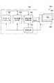
以下、本発明に係る電子機器を実施形態を挙げて説明する。なお、この実施形態は本発明の一例を示すものであり、本発明はこの実施形態に限定されるものではない。 Hereinafter, an electronic device according to the present invention will be described with reference to embodiments. In addition, this embodiment shows an example of this invention and this invention is not limited to this embodiment.
図19は、本発明に係る電子機器の一実施形態を示している。ここに示す電子機器は、液晶表示装置781と、これを制御する制御回路780とを有する。制御回路780は、表示情報処理回路785、電源回路786、タイミングジェネレータ787及び表示情報出力源788によって構成される。そして、液晶表示装置781は液晶パネル782、照明装置784及び駆動回路783を有する。 FIG. 19 shows an embodiment of an electronic apparatus according to the invention. The electronic device shown here includes a liquid
表示情報出力源788は、RAM(Random Access Memory)等といったメモリや、各種ディスク等といったストレージユニットや、デジタル画像信号を同調出力する同調回路等を備え、タイミングジェネレータ787により生成される各種のクロック信号に基づいて、所定フォーマットの画像信号等といった表示情報を表示情報処理回路785に供給する。 The display
次に、表示情報処理回路785は、増幅・反転回路や、ローテーション回路や、ガンマ補正回路や、クランプ回路等といった周知の回路を多数備え、入力した表示情報の処理を実行して、画像信号をクロック信号CLKと共に駆動回路783へ供給する。ここで、駆動回路783は、走査線駆動回路やデータ線駆動回路と共に、検査回路等を総称したものである。また、電源回路786は、上記の各構成要素に所定の電源電圧を供給する。 Next, the display
本発明は実施例の形態に限定されるものではなく、TNモードではなく負の誘電率異方性を持つ液晶を用いた垂直配向モード(VAモード)、横電界を利用したIPSモードの液晶表示装置に利用しても構わない。また、全透過型のみならず全反射型、反射透過兼用型であっても構わない。さらにアクティブ素子はポリシリコンTFTだけでなく、アモルファスシリコンTFTであってもよいし、その他のアクティブ素子であっても構わない。 The present invention is not limited to the form of the embodiment, but a vertical alignment mode (VA mode) using a liquid crystal having negative dielectric anisotropy instead of a TN mode, and an IPS mode liquid crystal display using a lateral electric field. You may use for an apparatus. Moreover, not only a total transmission type but also a total reflection type and a reflection / transmission combined type may be used. Further, the active element is not limited to the polysilicon TFT, but may be an amorphous silicon TFT or another active element.
11・・・アクティブマトリクス基板
13・・・走査線
15・・・データ線
17・・・容量線
45・・・画素電極
21・・・走査線駆動回路
23、123、223、323・・・データ線駆動回路
25・・・データ線プリチャージ回路DESCRIPTION OF
Claims (15)
Translated fromJapanese前記複数の走査線は、前記画素スイッチング素子に選択電位と非選択電位のいずれかの電位を与えるよう各々個別のタイミングで供給され、
前記対向電極は第1の電位と第2の電位の間で反転駆動し、
前記対向電極が前記第1の電位から前記第2の電位へ反転するコモン反転タイミングでは、前記複数の走査線のうち少なくとも1以上が前記選択電位にあることを特徴とする液晶表示装置の駆動方法。A plurality of scanning lines, a plurality of data lines arranged to intersect the plurality of scanning lines, a plurality of pixel electrodes arranged corresponding to the intersection of the plurality of scanning lines and the plurality of data lines, A driving method of a liquid crystal display device, comprising: a plurality of pixel switching elements that supply a signal of the data line to the pixel electrode based on a signal of the scanning line; and a counter electrode that is disposed to face the pixel electrode. And
The plurality of scanning lines are supplied at individual timings so as to apply either a selection potential or a non-selection potential to the pixel switching element,
The counter electrode is driven to invert between a first potential and a second potential,
A driving method of a liquid crystal display device, wherein at least one of the plurality of scanning lines is at the selection potential at a common inversion timing at which the counter electrode inverts from the first potential to the second potential. .
前記データ線は映像信号あるいはプリチャージ信号を供給する信号端子と電気的にハイインピーダンス状態にあり、前記画素電極との間を除きフローティング状態であることを特徴とする請求項1に記載の液晶表示装置の駆動方法。In the common inversion timing,
2. The liquid crystal display according to claim 1, wherein the data line is electrically in a high impedance state with a signal terminal for supplying a video signal or a precharge signal, and is in a floating state except between the pixel electrode and the data line. Device driving method.
前記走査線の前記比選択電位が前記第3の電位から前記第4の電位に反転駆動される走査線反転タイミングは前記コモン反転タイミングに略等しく、
第3の電位と第4の電位の差は第1の電位と第2の電位の差に略等しいことを特徴とする請求項1又は請求項2に記載の液晶表示装置の駆動方法。The non-selection potential supplied to the scan line is inverted and driven between a third potential and a fourth potential,
The scanning line inversion timing at which the ratio selection potential of the scanning line is inverted and driven from the third potential to the fourth potential is substantially equal to the common inversion timing,
3. The method for driving a liquid crystal display device according to claim 1, wherein a difference between the third potential and the fourth potential is substantially equal to a difference between the first potential and the second potential.
前記コモン反転タイミングは前記第1の非選択期間中であり、
前記第1の選択期間は前記第1の非選択期間より前であり、
前記第2の選択期間は前記第1の非選択期間より後であり、
前記第1の非選択期間の長さは第2の非選択期間より長いことを特徴とする請求項1から請求項4のいずれか一項に記載の液晶表示装置の駆動方法。During a scanning line selection period in which one of the plurality of scanning lines is at the selection potential, a first selection period for writing a video signal to a first data line of the plurality of data lines, and a first selection period of the plurality of data lines. A second selection period in which a video signal is written to two data lines, a first non-selection period in which a video signal is not written to all of the plurality of data lines, and a video signal is not written to all of the plurality of data lines. A second non-selection period,
The common inversion timing is during the first non-selection period;
The first selection period is before the first non-selection period;
The second selection period is after the first non-selection period;
5. The method of driving a liquid crystal display device according to claim 1, wherein the length of the first non-selection period is longer than that of the second non-selection period.
前記複数の走査線に交差して配置される複数のデータ線と、
前記複数の走査線と前記複数のデータ線の交差に対応して配置された複数の画素電極と、
前記走査線の信号に基づいて前記データ線の信号を前記画素電極に供給する複数の画素スイッチング素子と、
前記画素電極に対向配置され、第1の電位と第2の電位の間で反転するコモン電位が供給される対向電極と、
前記画素スイッチング素子に選択電位と非選択電位のいずれかの電位を与えるよう前記複数の走査線に各々個別のタイミングで供給すると共に、前記対向電極が前記第1の電位から前記第2の電位へ反転するコモン反転タイミングでは、前記複数の走査線のうち少なくとも1以上が前記選択電位とする走査線駆動回路とを備えることを特徴とする液晶表示装置。A plurality of scan lines;
A plurality of data lines arranged to intersect the plurality of scanning lines;
A plurality of pixel electrodes arranged corresponding to intersections of the plurality of scanning lines and the plurality of data lines;
A plurality of pixel switching elements that supply the data line signals to the pixel electrodes based on the scanning line signals;
A counter electrode disposed opposite to the pixel electrode and supplied with a common potential that is inverted between a first potential and a second potential;
The pixel switching element is supplied to each of the plurality of scanning lines at an individual timing so as to apply either a selection potential or a non-selection potential to the pixel switching element, and the counter electrode changes from the first potential to the second potential. A liquid crystal display device comprising: a scanning line driving circuit in which at least one of the plurality of scanning lines has the selection potential at a common inversion timing to be reversed.
前記データ線と前記走査線の容量をC1、
前記データ線と前記対向電極の容量をC2、
前記データ線と前記画素電極との容量、前記C1、前記C2を除く、前記データ線との容量をC3としたとき、
(C1÷n+C3)÷(C1+C2+C3)≦0.005を満たすことを特徴とする請求項8に記載の液晶表示装置。The number of scanning lines is n,
The capacitance of the data line and the scanning line is C1,
The capacitance of the data line and the counter electrode is C2,
When the capacitance between the data line and the pixel electrode, and the capacitance with the data line excluding C1 and C2, is C3,
9. The liquid crystal display device according to claim 8, wherein (C1 ÷ n + C3) ÷ (C1 + C2 + C3) ≦ 0.005 is satisfied.
前記コモン反転タイミングは前記第1の非選択期間中であり、前記第1の選択期間は前記第1の非選択期間より前であり、前記第2の選択期間は前記第1の非選択期間より後であり、前記第1の非選択期間の長さは第2の非選択期間より長くするよう制御するデータ線駆動回路を備えることを特徴とする請求項8又は請求項9に記載の液晶表示装置。During a scanning line selection period in which one of the plurality of scanning lines is at the selection potential, a first selection period for writing a video signal to a first data line of the plurality of data lines, and a first selection period of the plurality of data lines. A second selection period in which a video signal is written to two data lines, a first non-selection period in which a video signal is not written to all of the plurality of data lines, and a video signal is not written to all of the plurality of data lines. A second non-selection period,
The common inversion timing is during the first non-selection period, the first selection period is before the first non-selection period, and the second selection period is before the first non-selection period. 10. The liquid crystal display according to claim 8, further comprising a data line driving circuit that controls the length of the first non-selection period to be longer than that of the second non-selection period. apparatus.
前記データ線に前記第2の選択期間中に書き込む映像信号の振幅をΔV2とすると、
ΔV1はΔV2*{1+2*(C1÷n+C3)÷(C1+C2+C3)}に略等しいことを特徴とする請求項10に記載の液晶表示装置。The amplitude of the video signal written to the data line during the first selection period is ΔV1,
When the amplitude of the video signal written to the data line during the second selection period is ΔV2,
11. The liquid crystal display device according to claim 10, wherein ΔV1 is substantially equal to ΔV2 * {1 + 2 * (C1 ÷ n + C3) ÷ (C1 + C2 + C3)}.
前記第2のデータ線に接続された前記複数の画素電極の第2の画素電極とは同じ走査線に接続されてなり、
かつ互いに同じ色の表示に対応した画素であることを特徴とする請求項8から請求項11のいずれか一項に記載の液晶表示装置。A first pixel electrode of the plurality of pixel electrodes connected to the first data line;
A second pixel electrode of the plurality of pixel electrodes connected to the second data line is connected to the same scanning line;
12. The liquid crystal display device according to claim 8, wherein the liquid crystal display device is a pixel corresponding to display of the same color.
An electronic apparatus using the liquid crystal display device according to claim 7.
Priority Applications (4)
| Application Number | Priority Date | Filing Date | Title |
|---|---|---|---|
| JP2005100085AJP4419897B2 (en) | 2005-03-30 | 2005-03-30 | Liquid crystal display device driving method, liquid crystal display device, and electronic apparatus |
| US11/354,120US7646369B2 (en) | 2005-03-30 | 2006-02-15 | Method of driving liquid crystal display device, liquid crystal display device,and electronic apparatus |
| KR1020060028514AKR100798171B1 (en) | 2005-03-30 | 2006-03-29 | Driving method of liquid crystal display device, liquid crystal display device and electronic device |
| CNB200610066975XACN100495517C (en) | 2005-03-30 | 2006-03-30 | Driving method of liquid crystal display device, liquid crystal display device, and electronic equipment |
Applications Claiming Priority (1)
| Application Number | Priority Date | Filing Date | Title |
|---|---|---|---|
| JP2005100085AJP4419897B2 (en) | 2005-03-30 | 2005-03-30 | Liquid crystal display device driving method, liquid crystal display device, and electronic apparatus |
Publications (2)
| Publication Number | Publication Date |
|---|---|
| JP2006276794Atrue JP2006276794A (en) | 2006-10-12 |
| JP4419897B2 JP4419897B2 (en) | 2010-02-24 |
Family
ID=37030476
Family Applications (1)
| Application Number | Title | Priority Date | Filing Date |
|---|---|---|---|
| JP2005100085AExpired - LifetimeJP4419897B2 (en) | 2005-03-30 | 2005-03-30 | Liquid crystal display device driving method, liquid crystal display device, and electronic apparatus |
Country Status (4)
| Country | Link |
|---|---|
| US (1) | US7646369B2 (en) |
| JP (1) | JP4419897B2 (en) |
| KR (1) | KR100798171B1 (en) |
| CN (1) | CN100495517C (en) |
Cited By (3)
| Publication number | Priority date | Publication date | Assignee | Title |
|---|---|---|---|---|
| CN102087842A (en)* | 2009-12-03 | 2011-06-08 | 乐金显示有限公司 | LCD Monitor |
| US8405644B2 (en) | 2008-10-08 | 2013-03-26 | Sony Corporation | Electro-optical device, and electronic apparatus having the same |
| US11333910B2 (en) | 2018-11-20 | 2022-05-17 | Seiko Epson Corporation | Electro-optical device with a pre-charge circuit between pre-charge control signal lines |
Families Citing this family (14)
| Publication number | Priority date | Publication date | Assignee | Title |
|---|---|---|---|---|
| JP4154598B2 (en)* | 2003-08-26 | 2008-09-24 | セイコーエプソン株式会社 | Liquid crystal display device driving method, liquid crystal display device, and portable electronic device |
| KR100790977B1 (en)* | 2006-01-13 | 2008-01-03 | 삼성전자주식회사 | Output buffer with improved output deviation and source driver for flat panel display |
| EP2157565A4 (en)* | 2007-06-12 | 2012-01-04 | Sharp Kk | Liquid crystal display device, scan signal drive device, liquid crystal display device drive method, scan signal drive method, and television receiver |
| JP5260141B2 (en)* | 2008-05-22 | 2013-08-14 | パナソニック株式会社 | Display driving device, display module package, display panel module, and television set |
| FR2955964A1 (en)* | 2010-02-02 | 2011-08-05 | Commissariat Energie Atomique | IMAGE WRITING METHOD IN A LIQUID CRYSTAL DISPLAY |
| US20130021320A1 (en)* | 2011-07-18 | 2013-01-24 | Chimei Innolux Corporation | Pixel element, display panel thereof, and control method thereof |
| CN103913913B (en)* | 2013-12-10 | 2016-11-02 | 上海中航光电子有限公司 | An array substrate and its preparation method, display panel and display device |
| CN104155820B (en)* | 2014-08-13 | 2017-09-22 | 深圳市华星光电技术有限公司 | A kind of array base palte and driving method |
| KR102336183B1 (en)* | 2015-02-23 | 2021-12-07 | 삼성전자 주식회사 | Electronic device and power saving method therefor |
| CN105976747B (en)* | 2016-04-05 | 2019-11-22 | 上海中航光电子有限公司 | A display panel and its driving method |
| JP6780408B2 (en)* | 2016-09-26 | 2020-11-04 | セイコーエプソン株式会社 | Scanning line drive circuit, display driver, electro-optic device, electronic device and drive method |
| US10490154B2 (en)* | 2016-12-01 | 2019-11-26 | Seiko Epson Corporation | Electro-optical device and electronic device |
| CN107871478B (en)* | 2017-12-26 | 2020-11-13 | 深圳Tcl新技术有限公司 | Driving circuit and method of display module and display equipment |
| US11848333B2 (en)* | 2021-08-24 | 2023-12-19 | Innolux Corporation | Electronic device |
Family Cites Families (20)
| Publication number | Priority date | Publication date | Assignee | Title |
|---|---|---|---|---|
| JPS6249399A (en) | 1985-08-29 | 1987-03-04 | キヤノン株式会社 | display device |
| JP2982877B2 (en) | 1990-12-25 | 1999-11-29 | 日本電気株式会社 | Active matrix liquid crystal display |
| KR100474786B1 (en)* | 1995-12-14 | 2005-07-07 | 세이코 엡슨 가부시키가이샤 | Display method of operation, display device and electronic device |
| JPH09243997A (en)* | 1996-03-12 | 1997-09-19 | Toshiba Corp | Active matrix liquid crystal display device and driving method thereof |
| JPH11142815A (en) | 1997-11-10 | 1999-05-28 | Sony Corp | Liquid crystal display device |
| JP3512710B2 (en)* | 2000-05-30 | 2004-03-31 | Nec液晶テクノロジー株式会社 | Liquid crystal display |
| JP2001356741A (en)* | 2000-06-14 | 2001-12-26 | Sanyo Electric Co Ltd | Level shifter and active matrix type display device using the same |
| JP4123711B2 (en)* | 2000-07-24 | 2008-07-23 | セイコーエプソン株式会社 | Electro-optical panel driving method, electro-optical device, and electronic apparatus |
| US7088330B2 (en)* | 2000-12-25 | 2006-08-08 | Sharp Kabushiki Kaisha | Active matrix substrate, display device and method for driving the display device |
| JP3791354B2 (en)* | 2001-06-04 | 2006-06-28 | セイコーエプソン株式会社 | Operational amplifier circuit, drive circuit, and drive method |
| JP3820918B2 (en)* | 2001-06-04 | 2006-09-13 | セイコーエプソン株式会社 | Operational amplifier circuit, drive circuit, and drive method |
| JP3791355B2 (en)* | 2001-06-04 | 2006-06-28 | セイコーエプソン株式会社 | Driving circuit and driving method |
| KR100477598B1 (en) | 2001-10-08 | 2005-03-18 | 엘지.필립스 엘시디 주식회사 | Apparatus and Method for Driving Liquid Crystal Display of 2 Dot Inversion Type |
| JP2004317785A (en)* | 2003-04-16 | 2004-11-11 | Seiko Epson Corp | Driving method of electro-optical device, electro-optical device, and electronic apparatus |
| JP4154598B2 (en) | 2003-08-26 | 2008-09-24 | セイコーエプソン株式会社 | Liquid crystal display device driving method, liquid crystal display device, and portable electronic device |
| JP4148064B2 (en) | 2003-08-26 | 2008-09-10 | セイコーエプソン株式会社 | Liquid crystal display device driving method, liquid crystal display device, and portable electronic device |
| JP2005070541A (en) | 2003-08-26 | 2005-03-17 | Seiko Epson Corp | Liquid crystal display device and portable electronic device |
| JP2005300948A (en)* | 2004-04-13 | 2005-10-27 | Hitachi Displays Ltd | Display device and driving method thereof |
| JP5542297B2 (en)* | 2007-05-17 | 2014-07-09 | 株式会社半導体エネルギー研究所 | Liquid crystal display device, display module, and electronic device |
| JP5542296B2 (en)* | 2007-05-17 | 2014-07-09 | 株式会社半導体エネルギー研究所 | Liquid crystal display device, display module, and electronic device |
- 2005
- 2005-03-30JPJP2005100085Apatent/JP4419897B2/ennot_activeExpired - Lifetime
- 2006
- 2006-02-15USUS11/354,120patent/US7646369B2/enactiveActive
- 2006-03-29KRKR1020060028514Apatent/KR100798171B1/enactiveActive
- 2006-03-30CNCNB200610066975XApatent/CN100495517C/enactiveActive
Cited By (4)
| Publication number | Priority date | Publication date | Assignee | Title |
|---|---|---|---|---|
| US8405644B2 (en) | 2008-10-08 | 2013-03-26 | Sony Corporation | Electro-optical device, and electronic apparatus having the same |
| CN102087842A (en)* | 2009-12-03 | 2011-06-08 | 乐金显示有限公司 | LCD Monitor |
| CN102087842B (en)* | 2009-12-03 | 2013-07-17 | 乐金显示有限公司 | LCD Monitor |
| US11333910B2 (en) | 2018-11-20 | 2022-05-17 | Seiko Epson Corporation | Electro-optical device with a pre-charge circuit between pre-charge control signal lines |
Also Published As
| Publication number | Publication date |
|---|---|
| CN1841488A (en) | 2006-10-04 |
| KR20060105527A (en) | 2006-10-11 |
| US7646369B2 (en) | 2010-01-12 |
| KR100798171B1 (en) | 2008-01-24 |
| JP4419897B2 (en) | 2010-02-24 |
| CN100495517C (en) | 2009-06-03 |
| US20060232538A1 (en) | 2006-10-19 |
Similar Documents
| Publication | Publication Date | Title |
|---|---|---|
| KR100798171B1 (en) | Driving method of liquid crystal display device, liquid crystal display device and electronic device | |
| KR101318043B1 (en) | Liquid Crystal Display And Driving Method Thereof | |
| US7839374B2 (en) | Liquid crystal display device and method of driving the same | |
| KR100602761B1 (en) | Liquid-crystal display device and driving method thereof | |
| TWI397893B (en) | Liquid crystal device | |
| US8248338B2 (en) | Method of driving liquid crystal display device, liquid crystal display device, and portable electronic apparatus | |
| CN100487785C (en) | Electro-optical device, driving method therefor, and electronic apparatus | |
| US8294662B2 (en) | Electro-optical device, scan line driving circuit, and electronic apparatus | |
| KR100800490B1 (en) | Liquid crystal display and driving method thereof | |
| US7633592B2 (en) | Liquid crystal display device and electronic device | |
| KR20060021055A (en) | Liquid crystal display device, drive device and method for liquid crystal display device | |
| KR20070002544A (en) | Mobile LCD and Driving Method | |
| US7847775B2 (en) | Electro-optical device, method of driving electro-optical device, and electronic apparatus | |
| US8115719B2 (en) | Electro-optical device | |
| EP1600936A2 (en) | Active-matrix liquid-crystal display device | |
| JP4957169B2 (en) | Electro-optical device, scanning line driving circuit, and electronic apparatus | |
| KR20110067819A (en) | LCD and its driving method | |
| KR100898789B1 (en) | Driving Method of LCD | |
| KR20040110695A (en) | Apparatus and method for driving gate lines of liquid crystal display panel | |
| JP2009086171A (en) | Electro-optical device, method of driving electro-optical device, and electronic apparatus | |
| JP2005241741A (en) | Liquid crystal display device driving method, liquid crystal display device, and electronic apparatus | |
| JP2006337624A (en) | Driving method, driving circuit, electrooptical device, and electronic equipment |
Legal Events
| Date | Code | Title | Description |
|---|---|---|---|
| A977 | Report on retrieval | Free format text:JAPANESE INTERMEDIATE CODE: A971007 Effective date:20090401 | |
| A131 | Notification of reasons for refusal | Free format text:JAPANESE INTERMEDIATE CODE: A131 Effective date:20090714 | |
| A521 | Request for written amendment filed | Free format text:JAPANESE INTERMEDIATE CODE: A523 Effective date:20090908 | |
| TRDD | Decision of grant or rejection written | ||
| A01 | Written decision to grant a patent or to grant a registration (utility model) | Free format text:JAPANESE INTERMEDIATE CODE: A01 Effective date:20091110 | |
| A01 | Written decision to grant a patent or to grant a registration (utility model) | Free format text:JAPANESE INTERMEDIATE CODE: A01 | |
| A61 | First payment of annual fees (during grant procedure) | Free format text:JAPANESE INTERMEDIATE CODE: A61 Effective date:20091123 | |
| FPAY | Renewal fee payment (event date is renewal date of database) | Free format text:PAYMENT UNTIL: 20121211 Year of fee payment:3 | |
| R150 | Certificate of patent or registration of utility model | Ref document number:4419897 Country of ref document:JP Free format text:JAPANESE INTERMEDIATE CODE: R150 Free format text:JAPANESE INTERMEDIATE CODE: R150 | |
| S111 | Request for change of ownership or part of ownership | Free format text:JAPANESE INTERMEDIATE CODE: R313113 | |
| FPAY | Renewal fee payment (event date is renewal date of database) | Free format text:PAYMENT UNTIL: 20121211 Year of fee payment:3 | |
| R350 | Written notification of registration of transfer | Free format text:JAPANESE INTERMEDIATE CODE: R350 | |
| FPAY | Renewal fee payment (event date is renewal date of database) | Free format text:PAYMENT UNTIL: 20121211 Year of fee payment:3 | |
| S111 | Request for change of ownership or part of ownership | Free format text:JAPANESE INTERMEDIATE CODE: R313113 | |
| FPAY | Renewal fee payment (event date is renewal date of database) | Free format text:PAYMENT UNTIL: 20121211 Year of fee payment:3 | |
| R350 | Written notification of registration of transfer | Free format text:JAPANESE INTERMEDIATE CODE: R350 | |
| FPAY | Renewal fee payment (event date is renewal date of database) | Free format text:PAYMENT UNTIL: 20131211 Year of fee payment:4 | |
| R250 | Receipt of annual fees | Free format text:JAPANESE INTERMEDIATE CODE: R250 | |
| R250 | Receipt of annual fees | Free format text:JAPANESE INTERMEDIATE CODE: R250 | |
| R250 | Receipt of annual fees | Free format text:JAPANESE INTERMEDIATE CODE: R250 | |
| R250 | Receipt of annual fees | Free format text:JAPANESE INTERMEDIATE CODE: R250 | |
| R250 | Receipt of annual fees | Free format text:JAPANESE INTERMEDIATE CODE: R250 | |
| R250 | Receipt of annual fees | Free format text:JAPANESE INTERMEDIATE CODE: R250 | |
| R250 | Receipt of annual fees | Free format text:JAPANESE INTERMEDIATE CODE: R250 | |
| R250 | Receipt of annual fees | Free format text:JAPANESE INTERMEDIATE CODE: R250 | |
| R250 | Receipt of annual fees | Free format text:JAPANESE INTERMEDIATE CODE: R250 | |
| S111 | Request for change of ownership or part of ownership | Free format text:JAPANESE INTERMEDIATE CODE: R313111 | |
| R350 | Written notification of registration of transfer | Free format text:JAPANESE INTERMEDIATE CODE: R350 | |
| R250 | Receipt of annual fees | Free format text:JAPANESE INTERMEDIATE CODE: R250 | |
| R250 | Receipt of annual fees | Free format text:JAPANESE INTERMEDIATE CODE: R250 | |
| R250 | Receipt of annual fees | Free format text:JAPANESE INTERMEDIATE CODE: R250 | |
| R250 | Receipt of annual fees | Free format text:JAPANESE INTERMEDIATE CODE: R250 | |
| EXPY | Cancellation because of completion of term |