JP2006269534A - Semiconductor device and method for manufacturing the same, substrate for manufacturing the semiconductor device, method for manufacturing the same, and substrate for growing the semiconductor - Google Patents
Semiconductor device and method for manufacturing the same, substrate for manufacturing the semiconductor device, method for manufacturing the same, and substrate for growing the semiconductorDownload PDFInfo
- Publication number
- JP2006269534A JP2006269534AJP2005082308AJP2005082308AJP2006269534AJP 2006269534 AJP2006269534 AJP 2006269534AJP 2005082308 AJP2005082308 AJP 2005082308AJP 2005082308 AJP2005082308 AJP 2005082308AJP 2006269534 AJP2006269534 AJP 2006269534A
- Authority
- JP
- Japan
- Prior art keywords
- layer
- semiconductor
- gan
- electron
- substrate
- Prior art date
- Legal status (The legal status is an assumption and is not a legal conclusion. Google has not performed a legal analysis and makes no representation as to the accuracy of the status listed.)
- Pending
Links
Images


Classifications
- H—ELECTRICITY
- H10—SEMICONDUCTOR DEVICES; ELECTRIC SOLID-STATE DEVICES NOT OTHERWISE PROVIDED FOR
- H10D—INORGANIC ELECTRIC SEMICONDUCTOR DEVICES
- H10D30/00—Field-effect transistors [FET]
- H10D30/40—FETs having zero-dimensional [0D], one-dimensional [1D] or two-dimensional [2D] charge carrier gas channels
- H10D30/47—FETs having zero-dimensional [0D], one-dimensional [1D] or two-dimensional [2D] charge carrier gas channels having 2D charge carrier gas channels, e.g. nanoribbon FETs or high electron mobility transistors [HEMT]
- H10D30/471—High electron mobility transistors [HEMT] or high hole mobility transistors [HHMT]
- H10D30/472—High electron mobility transistors [HEMT] or high hole mobility transistors [HHMT] having lower bandgap active layer formed on top of wider bandgap layer, e.g. inverted HEMT
- H—ELECTRICITY
- H10—SEMICONDUCTOR DEVICES; ELECTRIC SOLID-STATE DEVICES NOT OTHERWISE PROVIDED FOR
- H10D—INORGANIC ELECTRIC SEMICONDUCTOR DEVICES
- H10D62/00—Semiconductor bodies, or regions thereof, of devices having potential barriers
- H10D62/10—Shapes, relative sizes or dispositions of the regions of the semiconductor bodies; Shapes of the semiconductor bodies
- H10D62/17—Semiconductor regions connected to electrodes not carrying current to be rectified, amplified or switched, e.g. channel regions
- H10D62/213—Channel regions of field-effect devices
- H10D62/221—Channel regions of field-effect devices of FETs
- H10D62/235—Channel regions of field-effect devices of FETs of IGFETs
- H—ELECTRICITY
- H10—SEMICONDUCTOR DEVICES; ELECTRIC SOLID-STATE DEVICES NOT OTHERWISE PROVIDED FOR
- H10D—INORGANIC ELECTRIC SEMICONDUCTOR DEVICES
- H10D62/00—Semiconductor bodies, or regions thereof, of devices having potential barriers
- H10D62/80—Semiconductor bodies, or regions thereof, of devices having potential barriers characterised by the materials
- H10D62/85—Semiconductor bodies, or regions thereof, of devices having potential barriers characterised by the materials being Group III-V materials, e.g. GaAs
- H10D62/8503—Nitride Group III-V materials, e.g. AlN or GaN
Landscapes
- Junction Field-Effect Transistors (AREA)
Abstract
Description
Translated fromJapanese本発明は半導体装置およびその製造方法、その半導体装置製造用基板及びその製造方法並びにその半導体成長用基板、特に、GaN系半導体装置及びその製造方法、その半導体装置製造用基板及びその製造方法並びにその半導体成長用基板に関する。The present invention relates to a semiconductor device and its manufacturing method, its semiconductor device manufacturing substrate and its manufacturing method, and its semiconductor growth substrate, in particular, a GaN-based semiconductor device and its manufacturing method, its semiconductor device manufacturing substrate and its manufacturing method, and its The present invention relates to a semiconductor growth substrate.
GaN系半導体、特に窒化ガリウム(GaN)を用いた半導体装置は、高周波かつ高出力で動作するパワー素子として用いられている。特に、マイクロ波、準ミリ波、ミリ波等の高周波帯域において増幅を行うのに適した半導体装置として、高電子移動度トランジスタ(High Electron Mobility Transistor:HEMT)が知られている。GaN系半導体とは、例えば、GaN若しくはGaNとAlNまたはInNの混晶である。 A semiconductor device using a GaN-based semiconductor, particularly gallium nitride (GaN), is used as a power element that operates at high frequency and high output. In particular, a high electron mobility transistor (HEMT) is known as a semiconductor device suitable for performing amplification in a high frequency band such as a microwave, a quasi-millimeter wave, and a millimeter wave. The GaN-based semiconductor is, for example, a mixed crystal of GaN or GaN and AlN or InN.
GaN系半導体を用いたHEMTにおいては、より高周波数動作、高出力動作を実現するための技術開発が進められている。高周波数動作、高出力動作を実現するため、2次元電子ガス(2 Dimensional Electron Gas:2DEG)の電子濃度を高くすること、ソース電極およびドレイン電極と2DEGとの接触抵抗(オーミック電極接触抵抗)を小さくすることが求められる。また、単一電源で動作可能な増幅器を提供するため、正の閾値電圧を有するエンハンスメント・モード(Eモード)のHEMTの技術開発も進められている。 In the HEMT using a GaN-based semiconductor, technological development for realizing higher frequency operation and higher output operation is underway. To realize high frequency operation and high output operation, increase the electron concentration of 2D electron gas (2 Dimensional Electron Gas: 2DEG), and contact resistance (ohmic electrode contact resistance) between the source and drain electrodes and 2DEG. It is required to be small. Further, in order to provide an amplifier that can operate with a single power supply, the technical development of an enhancement mode (E mode) HEMT having a positive threshold voltage is also underway.
HEMTには、電子走行層上に電子供給層を堆積し、該電子供給層上にゲート電極、ソース電極、およびドレイン電極を設けた通常型HEMTと、電子供給層上に電子走行層を堆積し、電子走行層上にゲート電極、ソース電極、およびドレイン電極を設けた反転型HEMTが知られている。 In the HEMT, an electron supply layer is deposited on the electron transit layer, a normal HEMT provided with a gate electrode, a source electrode, and a drain electrode on the electron supply layer, and an electron transit layer is deposited on the electron supply layer. An inversion HEMT in which a gate electrode, a source electrode, and a drain electrode are provided on an electron transit layer is known.
通常型HEMTについては特許文献1(従来例1)に開示されている。サファイア基板あるいはSiC基板上に、バッファ層を介し、不純物の添加されていないGaN電子走行層(特許文献1ではチャネル層)、電子走行層上にAlGaNスペーサ層を介しN型のAlGaN電子供給層が堆積され、電子供給層上にゲート電極、N型のGaNコンタクト層を介しソース電極およびドレイン電極が形成されている。 The normal HEMT is disclosed in Patent Document 1 (Conventional Example 1). On the sapphire substrate or SiC substrate, a GaN electron transit layer (channel layer in Patent Document 1) to which no impurity is added via a buffer layer, and an N-type AlGaN electron supply layer on the electron transit layer via an AlGaN spacer layer. A source electrode and a drain electrode are formed on the electron supply layer through a gate electrode and an N-type GaN contact layer.
一方、特許文献1においては、2DEGの電子濃度を増大させる手段として、電子供給層と電子走行層のバンドギャップの不連続エネルギーを大きくすることのみならず、電気的分極を用いることが記載されている。すなわち、自発分極とピエゾ分極の和により電子供給層と電子走行層の界面に正電荷が発生すれば、正電荷を打ち消すように電子が誘起し、2DEGの電子濃度が増大することが記載されている。従来例1においては、スペーサ層のAlN混晶比を一部大きくすることで、自発分極およびピエゾ分極に起因した正の電荷を2DEG付近に誘起させ2DEGの電子濃度を大きくすることが開示されている。 On the other hand, in
反転型HEMTについては特許文献2の図1(従来例2)に開示されている。サファイア基板の(0001)面にAlGaN下地層、下地層上に下地層よりAlNの混晶比の小さなN型のAlGaN電子供給層、電子供給層上に電子走行層(特許文献1においては電子蓄積層と記載)が堆積され、電子走行層上にゲート電極、ソース電極およびドレイン電極が形成されている。電子走行層の電子供給層界面付近には2DEGが形成されている。反転型HEMTにおいては、ソース電極およびドレイン電極と2DEGの間にバンドギャップの大きいAlGaN層が存在せず、オーミック電極接触抵抗が低減できる。
しかしながら、従来例1においては、通常型HEMTであるがゆえ、ソース電極およびドレイン電極と2DEGの間にバンドギャップの大きいAlGaN電子供給層が存在する。このため、オーミック電極接触抵抗が大きくなるという問題がある。 However, in the conventional example 1, since it is a normal type HEMT, an AlGaN electron supply layer having a large band gap exists between the source electrode and the drain electrode and 2DEG. For this reason, there exists a problem that ohmic electrode contact resistance becomes large.
一方、従来例2においては、2DEGの電子濃度が小さいという問題がある。以下、その原因について考察した結果を説明する。 On the other hand, Conventional Example 2 has a problem that the electron density of 2DEG is small. Hereinafter, the result of considering the cause will be described.
半導体層の電気的分極には、自発分極とピエゾ分極(圧電分極)がある。自発分極とは、電気陰性度の違いから分極するものであり、結晶種類と結晶方位から決まる。ピエゾ分極は、結晶が歪むことにより生じる分極であり、半導体層に、格子定数が異なる薄層が積層されると発生する。2層の半導体層の界面に誘起される電荷は両半導体層内の自発分極およびピエゾ分極の差となる。半導体層の2DEGの濃度は、自発分極とピエゾ分極との和になる。このことから、両者それぞれの働く向きが2DEGの濃度に影響する。 The electrical polarization of the semiconductor layer includes spontaneous polarization and piezoelectric polarization (piezoelectric polarization). Spontaneous polarization is polarization based on the difference in electronegativity and is determined by the crystal type and crystal orientation. Piezoelectric polarization is polarization that occurs when a crystal is distorted, and occurs when thin layers having different lattice constants are stacked on a semiconductor layer. The charge induced at the interface between the two semiconductor layers is the difference between spontaneous polarization and piezoelectric polarization in the two semiconductor layers. The concentration of 2DEG in the semiconductor layer is the sum of spontaneous polarization and piezoelectric polarization. For this reason, the working directions of both influence the concentration of 2DEG.
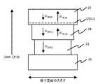
図1は従来例2のゲート電極下の各半導体層を模式的に表している。ここで、各層の横方向の長さは格子定数の大きさを模式的に表している。上方向がウルツ鉱構造の[0001]方向となる。(0001)サファイア基板20上に、AlGaN下地層22、AlGaN電子供給層24、GaN電子走行層26が堆積されている。GaN結晶やAlGaN結晶では[000−1]方向が正になるように自発分極する。自発分極の働く方向は、C軸に沿ったGa−Nの結合の向きで決まる。このため、[0001]方向(Ga面成長)では、下地層22、電子供給層24、および電子走行層26の自発分極PSP22、PSP24、およびPSP26が、下向きに働く(下向きが正となる)。また、AlN結晶はGaN結晶より自発分極が大きいため、AlN混晶比が大きいほど自発分極の絶対値は大きくなる。すなわち、以下の関係となる
下地層22は格子緩和する程度の厚膜として形成されているのため、下地層22の電子供給層24付近にはピエゾ分極はほとんど発生しない。電子供給層24および電子走行層26には下地層22との格子定数の違いによりピエゾ分極が発生する。電子供給層24および電子走行層26は、下地層22に比べ。格子定数が大きいため、電子供給層24および電子走行層26のピエゾ分極PPE24、およびPPE26は上向きに働く(上向きに正となる)。また、下地層22に対する格子定数は電子走行層26が電子供給層24より大きため、以下の関係になる。
[0001](Ga面成長)では、対象物(この場合には電子供給層24)に対して対象物と比較する電子走行層26の格子定数が大きい場合には、ピエゾ電荷は、上向きを正として働く。(ピエゾ分極の働く方向は、(1)結晶に加わる応力の向きと(2)結晶方位(Ga面、N面)で決まる。この場合には、前述の格子定数の大小の関係とGa面成長になることからピエゾ電荷は、上向きに働く) In [0001] (Ga plane growth), when the lattice constant of the
電子供給層24内の分極の和、と電子走行層26内の分極の和、の差が電子供給層24と電子走行層26の界面に発生する電荷となるから、電子供給層24と電子走行層26の界面には負の電荷が発生し、2DEGの電子濃度は減少する方向に働いてしまう。図1の場合には、自発分極とピエゾ分極がそれぞれ反対方向に働く。この場合、両者の分極が打ち消し合うため、分極電極が減少し、その結果、2DEGの電子濃度も減少する。 Since the difference between the sum of the polarization in the
以上のごとく、通常型HEMTにおいては自発分極とピエゾ分極を用い2DEGの電子濃度を増加させることが可能であるが、オーミック接触抵抗が大きい。一方、反転型HEMTにおいては、オーミック接触抵抗を減少させることが可能であるが、自己分極とピエゾ分極に起因し2DEGの電子濃度が小さいという問題がある。 As described above, in the normal HEMT, it is possible to increase the electron concentration of 2DEG using spontaneous polarization and piezo polarization, but the ohmic contact resistance is large. On the other hand, in the inverted HEMT, it is possible to reduce the ohmic contact resistance, but there is a problem that the electron concentration of 2DEG is low due to self-polarization and piezoelectric polarization.
また、従来例1および2においては、サファイア基板またはSiC基板にAlGaN膜またはGaN膜を堆積させている。AlGaN膜またはGaN膜の堆積の際、サファイア基板またはSiC基板には、まずGaが堆積するため、AlGaN膜またはGaN膜を[000−1]方向に堆積させることは容易ではなかった。 In the conventional examples 1 and 2, an AlGaN film or a GaN film is deposited on a sapphire substrate or SiC substrate. When depositing the AlGaN film or the GaN film, Ga is first deposited on the sapphire substrate or the SiC substrate. Therefore, it is not easy to deposit the AlGaN film or the GaN film in the [000-1] direction.
本発明の目的は、電子供給層および電子走行層を[000−1]方向に堆積させ、オーミック電極接触抵抗が小さく、かつ2DEGの電子濃度の大きい半導体装置及びその製造方法、その半導体装置製造用基板及びその製造方法並びにその半導体成長用基板を提供することである。 The object of the present invention is to deposit an electron supply layer and an electron transit layer in the [000-1] direction, have a low ohmic electrode contact resistance and a high 2DEG electron concentration, a method for manufacturing the semiconductor device, and a method for manufacturing the semiconductor device It is to provide a substrate, a manufacturing method thereof, and a semiconductor growth substrate.
本発明は、基板と相対する厚さ方向が[000−1]であるAlGaN電子供給層と、該電子供給層上に形成されたGaN電子走行層と、該電子走行層上に形成されたゲート電極と、該ゲート電極を挟み、前記電子走行層上に形成されたソース電極およびドレイン電極と、を備えたことを特徴とする半導体装置である。本発明によれば、電子供給層および電子走行層を[000−1]方向に形成させるため、ソース電極およびドレイン電極と2DEGの接触抵抗が小さく、かつ2DEGの電子濃度の大きい半導体装置を提供することが可能となる。 The present invention relates to an AlGaN electron supply layer whose thickness direction is [000-1] relative to the substrate, a GaN electron transit layer formed on the electron supply layer, and a gate formed on the electron transit layer. A semiconductor device comprising: an electrode; and a source electrode and a drain electrode formed on the electron transit layer with the gate electrode interposed therebetween. According to the present invention, since the electron supply layer and the electron transit layer are formed in the [000-1] direction, a semiconductor device having a low contact resistance between the source electrode and the drain electrode and 2DEG and a high electron concentration of 2DEG is provided. It becomes possible.
本発明は、前記電子走行層と前記ゲート電極の間に、AlGaN半導体層が設けられていることを特徴とする半導体装置とすることができる。また、本発明は、前記電子供給層は、300nm以下の膜厚を有することを特徴とする半導体装置とすることができる。さらに、本発明は、前記電子供給層は、0.25以下のAlNの混晶比を有することを特徴とする半導体装置とすることができる。 The present invention can provide a semiconductor device characterized in that an AlGaN semiconductor layer is provided between the electron transit layer and the gate electrode. In the semiconductor device according to the present invention, the electron supply layer has a thickness of 300 nm or less. Furthermore, the present invention can provide a semiconductor device wherein the electron supply layer has a mixed crystal ratio of AlN of 0.25 or less.
本発明は、基板と相対する厚さ方向が[000−1]方向であるAlGaN電子供給層とGaN電子走行層を順にMOCVD法を用い形成する第1のステップと、前記電子走行層上にゲート電極を形成する第2のステップと、前記電子走行層上に前記ゲート電極を挟んでソース電極およびドレイン電極を形成する第3のステップと、を備えることを特徴とする半導体装置の製造方法である。本発明によれば、電子供給層および電子走行層を[000−1]方向に形成させることができるため、ソース電極およびドレイン電極と2DEGの接触抵抗が小さく、かつ2DEGの電子濃度の大きい半導体装置の製造方法を提供することができる。 The present invention includes a first step of sequentially forming an AlGaN electron supply layer and a GaN electron transit layer whose thickness direction opposite to the substrate is a [000-1] direction by using a MOCVD method, and a gate on the electron transit layer. A method for manufacturing a semiconductor device, comprising: a second step of forming an electrode; and a third step of forming a source electrode and a drain electrode with the gate electrode interposed therebetween on the electron transit layer. . According to the present invention, since the electron supply layer and the electron transit layer can be formed in the [000-1] direction, the contact resistance between the source electrode and the drain electrode and 2DEG is low, and the semiconductor device has a high electron concentration of 2DEG. The manufacturing method of can be provided.
本発明は、前記第1のステップは、前記電子走行層上にAlGaN半導体層を形成するステップを含み、前記第3のステップは、前記半導体層上に前記ゲート電極を形成するステップであることを特徴とする半導体装置の製造方法とすることができる。また、本発明は、前記電子供給層は、300nm以下の膜厚で形成することを特徴とする半導体装置の製造方法とするこtができる。さらに、前記電子供給層は、0.25以下のAlN混晶比で形成することを特徴とする半導体装置の製造方法とすることができる。 According to the present invention, the first step includes a step of forming an AlGaN semiconductor layer on the electron transit layer, and the third step is a step of forming the gate electrode on the semiconductor layer. It can be set as the manufacturing method of the semiconductor device characterized. Further, the present invention can be a method for manufacturing a semiconductor device, wherein the electron supply layer is formed with a film thickness of 300 nm or less. Furthermore, the electron supply layer may be formed with an AlN mixed crystal ratio of 0.25 or less.
本発明は、主面が(000−1)面の半導体成長用基板と、該半導体成長用基板上に、[000−1]方向に成長されたGaN系半導体層と、を備えることを特徴とする半導体装置製造用基板である。本発明によれば、電子供給層および電子走行層を[000−1]方向に形成させることができ、ソース電極およびドレイン電極と2DEGの接触抵抗が小さく、かつ2DEGの電子濃度の大きい半導体装置を製造することができる半導体装置製造用基板を提供することができる。 The present invention includes a semiconductor growth substrate having a (000-1) plane as a principal surface, and a GaN-based semiconductor layer grown in the [000-1] direction on the semiconductor growth substrate. This is a substrate for manufacturing a semiconductor device. According to the present invention, a semiconductor device in which an electron supply layer and an electron transit layer can be formed in the [000-1] direction, the contact resistance between the source electrode and the drain electrode and 2DEG is small, and the electron concentration of 2DEG is large. A semiconductor device manufacturing substrate that can be manufactured can be provided.
本発明は、前記半導体成長用基板は、SiC、Si、サファイアおよびGaN系半導体のいずれか1つからなることを特徴とする半導体装置製造用基板とすることができる。また、本発明は、前記GaN系半導体層は、MOCVD法で形成されたことを特徴とする半導体装置製造用基板とすることができる。さらに、前記GaN系半導体層は、AlGaN電子供給層とGaN電子走行層が順にMOCVD法で形成された層を含むことを特徴とする半導体装置製造用基板とすることができる。 According to the present invention, the semiconductor growth substrate may be any one of SiC, Si, sapphire, and a GaN-based semiconductor. In the present invention, the GaN-based semiconductor layer may be a substrate for manufacturing a semiconductor device, wherein the substrate is formed by MOCVD. Furthermore, the GaN-based semiconductor layer can be a semiconductor device manufacturing substrate including a layer in which an AlGaN electron supply layer and a GaN electron transit layer are sequentially formed by MOCVD.
本発明は、主面が(000−1)面の半導体成長用基板上に[000−1]方向に、MOCVD法を用いGaN系半導体層を形成する工程を備えることを特徴とする半導体装置製造用基板の製造方法である。本発明によれば、電子供給層および電子走行層を[000−1]方向に形成させるため、ソース電極およびドレイン電極と2DEGの接触抵抗が小さく、かつ2DEGの電子濃度の大きい半導体装置を製造することができる半導体装置製造用基板の製造方法を提供することができる。 The present invention includes a process for forming a GaN-based semiconductor layer using a MOCVD method in a [000-1] direction on a semiconductor growth substrate having a (000-1) principal surface. It is a manufacturing method of the board | substrate. According to the present invention, since the electron supply layer and the electron transit layer are formed in the [000-1] direction, a semiconductor device having a low contact resistance between the source electrode and the drain electrode and 2DEG and a high electron concentration of 2DEG is manufactured. A method for manufacturing a substrate for manufacturing a semiconductor device can be provided.
本発明は、前記半導体成長用基板は、SiC、Si、サファイアおよびGaN系半導体のいずれか1つからなることを特徴とする半導体装置製造用基板の製造方法とすることができる。また、前記GaN半導体層を形成する工程の後に、AlGaN半導体層を形成する工程を備える半導体装置製造用基板の製造方法とすることができる。さらに、前記GaN系半導体層を形成す工程は、AlGaN電子供給層とGaN電子走行層を順に形成する工程を含むことを特徴とする半導体装置製造用基板の製造方法とすることができる。 The present invention can be a method for manufacturing a semiconductor device manufacturing substrate, wherein the semiconductor growth substrate is made of any one of SiC, Si, sapphire, and a GaN-based semiconductor. Moreover, it can be set as the manufacturing method of the board | substrate for semiconductor device manufacture provided with the process of forming an AlGaN semiconductor layer after the process of forming the said GaN semiconductor layer. Furthermore, the step of forming the GaN-based semiconductor layer may include a step of forming an AlGaN electron supply layer and a GaN electron transit layer in order, and a method for manufacturing a substrate for manufacturing a semiconductor device.
本発明は、成長用表面がGaN半導体層を[000−1]方向に成長させるための(000−1)面を主面とすることを特徴とする半導体成長用基板である。本発明によれば、電子供給層および電子走行層を[000−1]方向に形成させるため、ソース電極およびドレイン電極と2DEGの接触抵抗が小さく、かつ2DEGの電子濃度の大きい半導体装置を製造することができる半導体成長用基板を提供することができる。 The present invention is the substrate for semiconductor growth characterized in that the growth surface has a (000-1) plane as a main surface for growing a GaN semiconductor layer in the [000-1] direction. According to the present invention, since the electron supply layer and the electron transit layer are formed in the [000-1] direction, a semiconductor device having a low contact resistance between the source electrode and the drain electrode and 2DEG and a high electron concentration of 2DEG is manufactured. A semiconductor growth substrate that can be provided can be provided.
本発明は、前記半導体成長用基板は、SiC、Si,サファイアおよびGaN系半導体のいずれか1つからなることを特徴とする半導体成長用基板である。また、本発明は、前記GaN半導体層はMOCVDで成長する層であることを特徴とする半導体成長用基板である。さらに、前記GaN系半導体層は、AlGaN電子供給層とGaN電子走行層をこの順で形成する層を含むことを特徴とする半導体成長用基板である。 The present invention is the semiconductor growth substrate, wherein the semiconductor growth substrate is made of any one of SiC, Si, sapphire, and a GaN-based semiconductor. Further, the present invention is the substrate for semiconductor growth, wherein the GaN semiconductor layer is a layer grown by MOCVD. Furthermore, the GaN-based semiconductor layer is a semiconductor growth substrate including a layer in which an AlGaN electron supply layer and a GaN electron transit layer are formed in this order.
本発明によれば、電子供給層および電子走行層を[000−1]方向に
形成させるため、ソース電極およびドレイン電極と2DEGの接触抵抗が小さく、かつ2DEGの電子濃度の大きい半導体装置及びその製造方法、その半導体装置製造用基板及びその製造方法並びにその半導体成長用基板を提供することができる。According to the present invention, since the electron supply layer and the electron transit layer are formed in the [000-1] direction, the contact resistance between the source electrode and the drain electrode and 2DEG is low, and the semiconductor device has a high 2DEG electron concentration, and its manufacture It is possible to provide a method, a semiconductor device manufacturing substrate, a manufacturing method thereof, and a semiconductor growth substrate.
以下、図面を参照し本発明の実施例を説明する。 Embodiments of the present invention will be described below with reference to the drawings.
実施例1の断面図を図2に示す。GaN基板30(半導体成長用基板)の(000−1)面上に、基板面に対する厚さ方向が[000−1]であるSiをドープしたN型のAlGaN電子供給層32がMOCVD(Metal Organic Chemical Vapor Deposition)法を用い形成されている。電子供給層32の厚さは200nm、Siドナー濃度は1x1016cm−3、AlGaNのAlN混晶比は0.25である。電子供給層32の膜厚は電子供給層32が格子緩和しない厚さであり、300nm以下が好ましく、より好ましくは200nm以下である。例えば、200nm以下の場合には、AlGaN電子供給層32に働く応力が大きく発揮でき、ピエゾ分極の影響が大きく得られる。A sectional view of Example 1 is shown in FIG. On the (000-1) surface of the GaN substrate 30 (semiconductor growth substrate), an N-type AlGaN
さらに、ピエゾ分極の影響が得られる十分な電子供給層32の膜厚として10nm以上が好ましい。AlGaN電子供給層32のAlN混晶比は十分な分極の効果を得るため、0.3以下が好ましく、より好ましくは0.25以下である。混晶比が大きくなるとピエゾ電荷も大きくなる。その結果、2DEG濃度も大きくなる。しかし、例えば、電子供給層32の混晶比が0.3以上の場合には、電子走行層34であるGaN層との格子不整合が生じるため結晶性は劣化する。例えば、混晶比が0.25以下の場合には、電子走行層34であるGaN層との格子不整合が大きく改善される。また、半導体成長用基板としては、GaN基板が好ましいが、SiC基板、Si基板、サファイア基板を用いることもできる。 Furthermore, the film thickness of the sufficient
次に電子供給層32上に不純物を添加しないGaN電子走行層34がMOCVD法を用い形成されている。電子走行層34の電子供給層32界面付近には2DEG33が形成される。電子走行層34の厚さは20nmである。電子走行層34の厚さはオーミック電極接触抵抗が小さくなり、閾値電圧が大きくなる厚さ、50nm以下が好ましい、電子走行層34が例えば50nm以上と厚くなる場合には、ソース電極42およびドレイン電極44と、電子走行層34の距離が大きくなる。このため、ソース電極42およびドレイン電極44と2DEG33のコンタクト抵抗値が大きくなってしまう。また、ゲート電極の逆方向リーク電流が十分抑制できる厚み、5nm以上が好ましい。 Next, a GaN
これにより、GaN基板30(半導体成長用基板)と、GaN基板30(半導体成長用基板)上に[000−1]方向に成長されたGaN系半導体層とを備える半導体製造用基板が完成する。次に、電子走行層33上に蒸着法およびリフトオフ法を用い、ソース電極42およびドレイン電極44としてTi/Alが形成され、ゲート電極40としてNi/Auが形成されている。すなわち、ゲート電極40を挟みソース電極42およびドレイン電極44が形成されている。 Thus, a semiconductor manufacturing substrate including the GaN substrate 30 (semiconductor growth substrate) and the GaN-based semiconductor layer grown in the [000-1] direction on the GaN substrate 30 (semiconductor growth substrate) is completed. Next, Ti / Al is formed as the
実施例1においては、反転型HEMT構造のため、オーミック接触抵抗を小さくすることができる。また、2DEGの電子濃度を増大させることができる。その2DEGの電子濃度が増大する原理を以下に説明する。 In the first embodiment, the ohmic contact resistance can be reduced due to the inverted HEMT structure. In addition, the electron concentration of 2DEG can be increased. The principle of increasing the electron concentration of 2DEG will be described below.
図3は実施例1におけるゲート電極下の各半導体層を模式的に表している。ここで、各層の横方向の長さは格子定数の大きさを模式的に表している。上方向がウルツ鉱構造の「000−1」方向となる。GaN基板の(000−1)面上に、[000−1]方向に電子供給層32、電子走行層34が堆積されている。電子供給層32および電子走行層34の自発分極PSP32、およびPSP34は、上向きに働く(上向きが正となる)。自発分極は、[000−1](N面成長)では、C軸に沿ったGa−Nの結合の向きにより上向きに働く。また、以下の関係となる。
一方、電子供給層32はGaN基板30に対し格子定数が小さいため、[000−1]方向、すなわち上方向が正となり、PPE32のピエゾ分極が生じる。電子供給層32は、厚く積まれていないため格子緩和されない。その結果、電子供給層32には応力が発生する。[000−1](N面成長)では、対象物(この場合には、基板)に対して、対象物に比較する電子供給層32の格子定数が小さい場合には、ピエゾ分極は上向きに働く。例えば、GaN結晶の格子定数は0.3189nmに対し、AlN混晶比0.25のAlGaN結晶の格子定数は0.3170nmである。走行層34はGaN基板30と同じ格子定数のためピエゾ分極は発生しない。On the other hand, since the
以上より、電子供給層32と電子走行層34の界面には、自発分極およびピエゾ分極に起因し正電荷が発生する。このため、2DEGの電子濃度を増加させることができる。従来例2においては、2DEGの電子濃度は8.1x1012cm−2であったが、実施例1においては、1.3x1013cm−2の2DEG電子濃度が得られた。As described above, positive charges are generated at the interface between the
図4は実施例1の変形例である。GaN基板30に電子供給層32を堆積させる工程の前に、GaN基板30の(000−1)面にMOCVD法により、GaNバッファ層38を堆積させている。この結果、GaNバッファ層38の上層の結晶性が向上する。GaN基板30とGaNバッファ層38は同じGaNであるため、本変形例においても、実施例1と同様の効果が生じる。 FIG. 4 shows a modification of the first embodiment. Before the step of depositing the
実施例2の断面図を図5に示す。実施例2は、AlGaNバリア層36(AlGaN半導体層)を具備することにより、より高性能なEモードを可能とする反転型HEMTである。以下製造方法について説明する。 A sectional view of Example 2 is shown in FIG. Example 2 is an inversion HEMT that enables an E-mode with higher performance by including an AlGaN barrier layer 36 (AlGaN semiconductor layer). The manufacturing method will be described below.
まず、図6において、GaN基板の(000−1)面上に、MOCVD法を用い、[000−1]方向にSi添加したN型のAlGaN電子供給層を形成させる。電子供給層32の膜厚は300nm、ドナー濃度は1x1016cm−3、AlN混晶比は0.25である。次に、MOCVD法を用い、電子供給層32上にGaN電子走行層34を形成させる。電子走行層34の厚さは10nmである。電子走行層34の厚さが10nm以下と薄いのはEモードの閾値電圧を所望するためである。例えば、電子走行層34の厚さが10nm以上と厚くなる場合には、P型のバリア層36と2DEG33との距離が大きくなる。このため、空乏層が低減して閾値電圧が負方向にシフトする。その結果、閾値電圧が0Vを下回ればEモードからDモードとなる。次に、MOCVD法を用い、電子走行層34上にP型のAlGaNバリア層36(AlGaN半導体層)を形成させる。バリア層36の厚さは200nm、アクセプタ濃度は2x1018cm−3、混晶比は0.3である。このとき、電子走行層33の電子供給層32界面には2DEG33、電子走行層33のバリア層36界面には2DHG35が形成される。これにより半導体装置製造用基板が完成する。First, in FIG. 6, an N-type AlGaN electron supply layer to which Si is added in the [000-1] direction is formed on the (000-1) plane of the GaN substrate by using the MOCVD method. The thickness of the
次に、図7において、ソース電極およびドレイン電極形成予定領域のバリア層36をドライエッチング法またはウェットエッチング法により除去する。または、バリア層36は電子走行層33上に、例えば酸化シリコン膜をマスクにして、ゲート電極40形成領域にのみ選択成長することも可能である。 Next, in FIG. 7, the
次に、図8において、電子走行層33上に、蒸着法およびリフトオフ法により、ソースで電極およびドレイン電極としてTi/Alを形成する。最後に、バリア層36上に、蒸着法およびリフトオフ法を用い、ゲート電極40としてNi/Auを形成し、図5の反転型HEMTが完成する。 Next, in FIG. 8, Ti / Al is formed on the
図9は実施例2におけるゲート電極下の各半導体層を模式的に表している。ここで、各層の横方向の長さは格子定数の大きさを模式的に表している。上方向がウルツ鉱構造の「000−1」方向となる。GaN基板の(000−1)面上に、[000−1]方向に電子供給層32、電子走行層34、バリア層36を堆積している。電子供給層32、電子走行層34、バリア層36の自発分極PSP32、PSP34、PSP36は、[000−1]方向、すなわち上向きが正となる。また、以下の関係となる
一方、電子供給層32およびバリア層36は、GaN基板30に対し格子定数が小さいため、電子供給層32およびバリア層36のピエゾ分極PPE32、およびPPE36は上方向が正となる。電子走行層34はGaN基板30と同じ格子定数のためピエゾ分極は発生しない。On the other hand, since the
以上より、電子供給層32と電子走行層34の界面には、自発分極およびピエゾ分極に起因した正の電荷が発生する。これにより、実施例1同様に2DEG33の電子濃度を増加させることができる。また、電子走行層34とバリア層36の界面には、自発分極およびピエゾ分極に起因した負の電荷が発生する。これにより、電子走行層34のバリア層36界面に発生した2DHG35のホール濃度を増加させることができる。 As described above, positive charges due to spontaneous polarization and piezoelectric polarization are generated at the interface between the
一方、実施例1においては、性能の良好なEモードを得ることは容易ではなかった。これは、閾値電圧を正とするためには、電子走行層34を薄くすることが必要である。しかし、電子走行層34が薄くなると、ゲート電極のリーク電流が大きくなるためである。また、ピンチオフ特性も悪くなってしまう。そこで、実施例2においては、電子走行層34上にバンドギャップが大きく、電子、ホールにとって障壁となるバリア層36が配置されている。バリア層36により、電子走行層34を薄くしてもゲート電極のリーク電流を抑制できる。また、バリア層36と2DHG35により、ゲート電極直下の空乏層の伸びを大きくし、ピンチオフ特性の良いEモードのHEMTを実現できる。 On the other hand, in Example 1, it was not easy to obtain an E mode with good performance. In order to make the threshold voltage positive, it is necessary to make the
図10に実施例2のドレイン電流(Ids)−ゲート・ソース電圧(Vgs)特性を示す。本実施例においては、電子供給層32は不純物を添加しないAlNの混晶比0.25のAlGaN層、電子走行層34は不純物を添加しないGaN層20nm、バリア層はアプセクタ濃度2x1018cm−3で混晶比0.25のAlGaN層30nmである。実施例2に係るHEMTにおいては、Vgsが負の領域ではIdが流れておらず、良好なピンチオフ特性を示している。これは、バリア層36および2DEG35により、ゲート電極直下の空乏層が伸びたためである。これにより、良好なEモードのHEMTが実現できている。FIG. 10 shows the drain current (Ids) -gate-source voltage (Vgs) characteristics of Example 2. In the present embodiment, the
以上のように、実施例1および実施例2においては、電子供給層および電子走行層を[000−1]方向に形成させることができるため、ソース電極およびドレイン電極と2DEGの接触抵抗が小さく、かつ2DEGの電子濃度の大きい半導体装置およびその製造方法、半導体装置製造用基板およびその製造方法を提供することができる。さらに、成長用表面がGaN系半導体層を[000−1]に成長させるための(000−1)面を主面とする半導体成長用基板もGaN系半導体層を[000−1]に成長させることにより同様の効果が得られる。 As described above, in Example 1 and Example 2, since the electron supply layer and the electron transit layer can be formed in the [000-1] direction, the contact resistance between the source electrode and the drain electrode and 2DEG is small. In addition, it is possible to provide a semiconductor device having a high electron concentration of 2DEG and a manufacturing method thereof, a substrate for manufacturing a semiconductor device, and a manufacturing method thereof. Further, the growth surface of the semiconductor growth substrate having a (000-1) plane as a main surface for growing the GaN-based semiconductor layer to [000-1] also grows the GaN-based semiconductor layer to [000-1]. Thus, the same effect can be obtained.
以上、本発明の好ましい実施形態について詳述したが、本発明は係る特定の実施形態に限定されるものではなく、特許請求の範囲に記載された本発明の要旨の範囲内において、種々の変形・変更が可能である。例えば、電子供給層32と電子走行層34の間にAlGaNストッパ層を配置し、あるいは電子供給層内で不純物のドープ濃度を変化させる等の変更を行うこともできる。 The preferred embodiments of the present invention have been described in detail above, but the present invention is not limited to such specific embodiments, and various modifications can be made within the scope of the gist of the present invention described in the claims.・ Change is possible. For example, an AlGaN stopper layer may be disposed between the
20 サファイア基板
22 AlGaNバッファ層
24 AlGaN電子供給層
26 GaN電子走行層
30 GaN基板
32 AlGaAs電子供給層
33 2DEG
34 電子走行層
35 2DHG
36 AlGaNバリア層
38 GaNバッファ層
40 ゲート電極
42 ソース電極
44 ドレイン電極
20
34
36
Claims (20)
Translated fromJapanese該電子供給層上に形成されたGaN電子走行層と、
該電子走行層上に形成されたゲート電極と、
該ゲート電極を挟み、前記電子走行層上に形成されたソース電極およびドレイン電極と、を備えたことを特徴とする半導体装置。An AlGaN electron supply layer whose thickness direction with respect to the substrate surface is [000-1];
A GaN electron transit layer formed on the electron supply layer;
A gate electrode formed on the electron transit layer;
A semiconductor device comprising: a source electrode and a drain electrode formed on the electron transit layer with the gate electrode interposed therebetween.
前記電子走行層上にゲート電極を形成する第2のステップと、
前記電子走行層上に前記ゲート電極を挟んでソース電極およびドレイン電極を形成する第3のステップと、を備えることを特徴とする半導体装置の製造方法。A first step of sequentially forming an AlGaN electron supply layer and a GaN electron transit layer whose thickness direction with respect to the substrate surface is the [000-1] direction by using the MOCVD method;
A second step of forming a gate electrode on the electron transit layer;
And a third step of forming a source electrode and a drain electrode across the gate electrode on the electron transit layer.
前記第3のステップは、前記AlGaN半導体層上に前記ゲート電極を形成するステップであることを特徴とする請求項5記載の半導体装置の製造方法。The first step includes forming an AlGaN semiconductor layer on the electron transit layer,
6. The method of manufacturing a semiconductor device according to claim 5, wherein the third step is a step of forming the gate electrode on the AlGaN semiconductor layer.
該半導体成長用基板上に、[000−1]方向に成長されたGaN系半導体層と、を備えることを特徴とする半導体装置製造用基板。A semiconductor growth substrate having a (000-1) principal surface;
A semiconductor device manufacturing substrate comprising: a GaN-based semiconductor layer grown in the [000-1] direction on the semiconductor growth substrate.
18. The semiconductor growth substrate according to claim 17, wherein the GaN-based semiconductor layer includes a layer in which an AlGaN electron supply layer and a GaN electron transit layer are formed in this order.
Priority Applications (2)
| Application Number | Priority Date | Filing Date | Title |
|---|---|---|---|
| JP2005082308AJP2006269534A (en) | 2005-03-22 | 2005-03-22 | Semiconductor device and method for manufacturing the same, substrate for manufacturing the semiconductor device, method for manufacturing the same, and substrate for growing the semiconductor |
| US11/385,749US7521707B2 (en) | 2005-03-22 | 2006-03-22 | Semiconductor device having GaN-based semiconductor layer |
Applications Claiming Priority (1)
| Application Number | Priority Date | Filing Date | Title |
|---|---|---|---|
| JP2005082308AJP2006269534A (en) | 2005-03-22 | 2005-03-22 | Semiconductor device and method for manufacturing the same, substrate for manufacturing the semiconductor device, method for manufacturing the same, and substrate for growing the semiconductor |
Publications (2)
| Publication Number | Publication Date |
|---|---|
| JP2006269534Atrue JP2006269534A (en) | 2006-10-05 |
| JP2006269534A5 JP2006269534A5 (en) | 2008-05-01 |
Family
ID=37034326
Family Applications (1)
| Application Number | Title | Priority Date | Filing Date |
|---|---|---|---|
| JP2005082308APendingJP2006269534A (en) | 2005-03-22 | 2005-03-22 | Semiconductor device and method for manufacturing the same, substrate for manufacturing the semiconductor device, method for manufacturing the same, and substrate for growing the semiconductor |
Country Status (2)
| Country | Link |
|---|---|
| US (1) | US7521707B2 (en) |
| JP (1) | JP2006269534A (en) |
Cited By (20)
| Publication number | Priority date | Publication date | Assignee | Title |
|---|---|---|---|---|
| JP2006310644A (en)* | 2005-04-28 | 2006-11-09 | Sumitomo Electric Ind Ltd | Field effect transistor and epitaxial substrate |
| US7425721B2 (en) | 2006-05-23 | 2008-09-16 | Sharp Kabushiki Kaisha | Field-effect transistor |
| JP2009004421A (en)* | 2007-06-19 | 2009-01-08 | Nec Corp | Semiconductor device |
| JP2009509343A (en)* | 2005-09-16 | 2009-03-05 | ザ リージェンツ オブ ザ ユニバーシティ オブ カリフォルニア | N pole aluminum gallium nitride / gallium nitride enhancement mode field effect transistor |
| WO2009116281A1 (en)* | 2008-03-19 | 2009-09-24 | 住友化学株式会社 | Semiconductor device and manufacturing method for the same |
| JP2010517261A (en)* | 2007-01-22 | 2010-05-20 | エレメント シックス リミテッド | ELECTRONIC FIELD EFFECT DEVICE AND METHOD FOR MANUFACTURING THE SAME |
| JP2010199321A (en)* | 2009-02-25 | 2010-09-09 | Fujitsu Ltd | Compound semiconductor device and method for manufacturing same |
| JP2011003808A (en)* | 2009-06-19 | 2011-01-06 | Nec Corp | Field effect transistor and method of manufacturing the same |
| JP2011108712A (en)* | 2009-11-13 | 2011-06-02 | New Japan Radio Co Ltd | Nitride semiconductor device |
| US8164117B2 (en) | 2008-10-27 | 2012-04-24 | Sanken Electric Co., Ltd. | Nitride semiconductor device |
| JP2013074179A (en)* | 2011-09-28 | 2013-04-22 | Fujitsu Ltd | Compound semiconductor device and manufacturing method of the same |
| US8546848B2 (en) | 2008-10-15 | 2013-10-01 | Sanken Electric Co., Ltd. | Nitride semiconductor device |
| JP5388839B2 (en)* | 2007-02-28 | 2014-01-15 | ルネサスエレクトロニクス株式会社 | Group III nitride semiconductor field effect transistor |
| JP2014197644A (en)* | 2013-03-29 | 2014-10-16 | トランスフォーム・ジャパン株式会社 | Compound semiconductor device and method of manufacturing the same |
| JP5718458B2 (en)* | 2011-05-16 | 2015-05-13 | ルネサスエレクトロニクス株式会社 | Field effect transistor and semiconductor device |
| JP2015095483A (en)* | 2013-11-08 | 2015-05-18 | 住友電気工業株式会社 | Group III nitride semiconductor device |
| JP2016187025A (en)* | 2015-03-27 | 2016-10-27 | 富士通株式会社 | Semiconductor device |
| WO2021234813A1 (en)* | 2020-05-19 | 2021-11-25 | 日本電信電話株式会社 | Method for fabricating field-effect transistor |
| WO2023085524A1 (en)* | 2021-11-15 | 2023-05-19 | 엘앤디전자 주식회사 | Semiconductor active element |
| JP2024543256A (en)* | 2021-11-25 | 2024-11-20 | 華為技術有限公司 | High electron mobility transistor, radio frequency transistor, power amplifier and method for manufacturing high electron mobility transistor |
Families Citing this family (16)
| Publication number | Priority date | Publication date | Assignee | Title |
|---|---|---|---|---|
| ATE359602T1 (en)* | 2000-06-02 | 2007-05-15 | Microgan Gmbh | HETEROSTRUCTURE WITH BACK DONATOR DOPPING |
| JP4705482B2 (en)* | 2006-01-27 | 2011-06-22 | パナソニック株式会社 | Transistor |
| JP5362187B2 (en)* | 2006-03-30 | 2013-12-11 | 日本碍子株式会社 | Semiconductor element |
| JP4282708B2 (en)* | 2006-10-20 | 2009-06-24 | 株式会社東芝 | Nitride semiconductor devices |
| CA2669228C (en)* | 2006-11-15 | 2014-12-16 | The Regents Of The University Of California | Method for heteroepitaxial growth of high-quality n-face gan, inn, and ain and their alloys by metal organic chemical vapor deposition |
| US8193020B2 (en)* | 2006-11-15 | 2012-06-05 | The Regents Of The University Of California | Method for heteroepitaxial growth of high-quality N-face GaN, InN, and AlN and their alloys by metal organic chemical vapor deposition |
| WO2008121976A2 (en)* | 2007-03-29 | 2008-10-09 | The Regents Of The University Of California | Method to fabricate iii-n semiconductor devices on the n-face of layers which are grown in the iii-face direction using wafer bonding and substrate removal |
| US20090085065A1 (en)* | 2007-03-29 | 2009-04-02 | The Regents Of The University Of California | Method to fabricate iii-n semiconductor devices on the n-face of layers which are grown in the iii-face direction using wafer bonding and substrate removal |
| US8455920B2 (en)* | 2007-05-23 | 2013-06-04 | International Rectifier Corporation | III-nitride heterojunction device |
| US7728356B2 (en)* | 2007-06-01 | 2010-06-01 | The Regents Of The University Of California | P-GaN/AlGaN/AlN/GaN enhancement-mode field effect transistor |
| US7875537B2 (en)* | 2007-08-29 | 2011-01-25 | Cree, Inc. | High temperature ion implantation of nitride based HEMTs |
| KR101774933B1 (en)* | 2010-03-02 | 2017-09-06 | 삼성전자 주식회사 | High Electron Mobility Transistor representing dual depletion and method of manufacturing the same |
| EP2610912A4 (en) | 2010-08-27 | 2014-10-22 | Nat Univ Corp Nara Inst | SiC SEMICONDUCTOR ELEMENT |
| CN112652659B (en) | 2019-10-09 | 2024-02-13 | 联华电子股份有限公司 | High electron mobility transistor and manufacturing method thereof |
| CN112951963B (en)* | 2021-02-09 | 2023-10-13 | 华灿光电(浙江)有限公司 | Light-emitting diode epitaxial wafer and preparation method thereof |
| CN114725019B (en)* | 2022-01-06 | 2025-07-11 | 西安电子科技大学 | An N-face GaN-based p- and n-channel device integrated structure and preparation method thereof |
Citations (3)
| Publication number | Priority date | Publication date | Assignee | Title |
|---|---|---|---|---|
| JPH11340510A (en)* | 1998-03-27 | 1999-12-10 | Sharp Corp | Semiconductor device and manufacturing method thereof |
| JP2000294768A (en)* | 1999-04-01 | 2000-10-20 | Sony Corp | Semiconductor device and method of manufacturing the same |
| JP2006261179A (en)* | 2005-03-15 | 2006-09-28 | Hitachi Cable Ltd | Semiconductor wafer and manufacturing method thereof |
Family Cites Families (3)
| Publication number | Priority date | Publication date | Assignee | Title |
|---|---|---|---|---|
| JP2001077353A (en)* | 1999-06-30 | 2001-03-23 | Toshiba Corp | High electron mobility transistor and power amplifier |
| JP4117535B2 (en) | 2001-11-30 | 2008-07-16 | 信越半導体株式会社 | Compound semiconductor device |
| US20050077538A1 (en)* | 2003-10-10 | 2005-04-14 | The Regents Of The University Of California | Design methodology for multiple channel heterostructures in polar materials |
- 2005
- 2005-03-22JPJP2005082308Apatent/JP2006269534A/enactivePending
- 2006
- 2006-03-22USUS11/385,749patent/US7521707B2/ennot_activeExpired - Fee Related
Patent Citations (3)
| Publication number | Priority date | Publication date | Assignee | Title |
|---|---|---|---|---|
| JPH11340510A (en)* | 1998-03-27 | 1999-12-10 | Sharp Corp | Semiconductor device and manufacturing method thereof |
| JP2000294768A (en)* | 1999-04-01 | 2000-10-20 | Sony Corp | Semiconductor device and method of manufacturing the same |
| JP2006261179A (en)* | 2005-03-15 | 2006-09-28 | Hitachi Cable Ltd | Semiconductor wafer and manufacturing method thereof |
Cited By (20)
| Publication number | Priority date | Publication date | Assignee | Title |
|---|---|---|---|---|
| JP2006310644A (en)* | 2005-04-28 | 2006-11-09 | Sumitomo Electric Ind Ltd | Field effect transistor and epitaxial substrate |
| JP2009509343A (en)* | 2005-09-16 | 2009-03-05 | ザ リージェンツ オブ ザ ユニバーシティ オブ カリフォルニア | N pole aluminum gallium nitride / gallium nitride enhancement mode field effect transistor |
| US7425721B2 (en) | 2006-05-23 | 2008-09-16 | Sharp Kabushiki Kaisha | Field-effect transistor |
| JP2010517261A (en)* | 2007-01-22 | 2010-05-20 | エレメント シックス リミテッド | ELECTRONIC FIELD EFFECT DEVICE AND METHOD FOR MANUFACTURING THE SAME |
| JP5388839B2 (en)* | 2007-02-28 | 2014-01-15 | ルネサスエレクトロニクス株式会社 | Group III nitride semiconductor field effect transistor |
| JP2009004421A (en)* | 2007-06-19 | 2009-01-08 | Nec Corp | Semiconductor device |
| WO2009116281A1 (en)* | 2008-03-19 | 2009-09-24 | 住友化学株式会社 | Semiconductor device and manufacturing method for the same |
| US8546848B2 (en) | 2008-10-15 | 2013-10-01 | Sanken Electric Co., Ltd. | Nitride semiconductor device |
| US8164117B2 (en) | 2008-10-27 | 2012-04-24 | Sanken Electric Co., Ltd. | Nitride semiconductor device |
| JP2010199321A (en)* | 2009-02-25 | 2010-09-09 | Fujitsu Ltd | Compound semiconductor device and method for manufacturing same |
| JP2011003808A (en)* | 2009-06-19 | 2011-01-06 | Nec Corp | Field effect transistor and method of manufacturing the same |
| JP2011108712A (en)* | 2009-11-13 | 2011-06-02 | New Japan Radio Co Ltd | Nitride semiconductor device |
| JP5718458B2 (en)* | 2011-05-16 | 2015-05-13 | ルネサスエレクトロニクス株式会社 | Field effect transistor and semiconductor device |
| JP2013074179A (en)* | 2011-09-28 | 2013-04-22 | Fujitsu Ltd | Compound semiconductor device and manufacturing method of the same |
| JP2014197644A (en)* | 2013-03-29 | 2014-10-16 | トランスフォーム・ジャパン株式会社 | Compound semiconductor device and method of manufacturing the same |
| JP2015095483A (en)* | 2013-11-08 | 2015-05-18 | 住友電気工業株式会社 | Group III nitride semiconductor device |
| JP2016187025A (en)* | 2015-03-27 | 2016-10-27 | 富士通株式会社 | Semiconductor device |
| WO2021234813A1 (en)* | 2020-05-19 | 2021-11-25 | 日本電信電話株式会社 | Method for fabricating field-effect transistor |
| WO2023085524A1 (en)* | 2021-11-15 | 2023-05-19 | 엘앤디전자 주식회사 | Semiconductor active element |
| JP2024543256A (en)* | 2021-11-25 | 2024-11-20 | 華為技術有限公司 | High electron mobility transistor, radio frequency transistor, power amplifier and method for manufacturing high electron mobility transistor |
Also Published As
| Publication number | Publication date |
|---|---|
| US20060214188A1 (en) | 2006-09-28 |
| US7521707B2 (en) | 2009-04-21 |
Similar Documents
| Publication | Publication Date | Title |
|---|---|---|
| JP2006269534A (en) | Semiconductor device and method for manufacturing the same, substrate for manufacturing the semiconductor device, method for manufacturing the same, and substrate for growing the semiconductor | |
| US20210313462A1 (en) | Nitride semiconductor device | |
| JP5348364B2 (en) | Heterojunction field effect semiconductor device | |
| JP5397825B2 (en) | Field effect semiconductor device | |
| JP5245305B2 (en) | Field effect semiconductor device and manufacturing method thereof | |
| US7777254B2 (en) | Normally-off field-effect semiconductor device | |
| JP4663156B2 (en) | Compound semiconductor device | |
| JP5084262B2 (en) | Semiconductor device | |
| JP6174874B2 (en) | Semiconductor device | |
| JP4744109B2 (en) | Semiconductor device and manufacturing method thereof | |
| JP5684574B2 (en) | Semiconductor device | |
| JP4729067B2 (en) | Field effect transistor | |
| JP5190923B2 (en) | Nitride semiconductor transistor having GaN as channel layer and manufacturing method thereof | |
| CN103035696B (en) | Compound semiconductor device and the method for the manufacture of compound semiconductor device | |
| JP2009099691A (en) | Method of manufacturing field-effect semiconductor device | |
| JP2002016087A (en) | Semiconductor device | |
| CN103548127A (en) | Semiconductor device and manufacturing method thereof | |
| JPWO2007122790A1 (en) | Field effect transistor | |
| JP2012231003A (en) | Semiconductor device | |
| WO2011024754A1 (en) | Group iii nitride laminated semiconductor wafer and group iii nitride semiconductor device | |
| CN105244377A (en) | Silicon substrate based HEMT device and manufacturing method thereof | |
| JP2011108712A (en) | Nitride semiconductor device | |
| JP5581601B2 (en) | Compound semiconductor device and manufacturing method thereof | |
| JP2011210785A (en) | Field-effect transistor and method for manufacturing the same | |
| JP2012230991A (en) | Semiconductor device |
Legal Events
| Date | Code | Title | Description |
|---|---|---|---|
| A521 | Request for written amendment filed | Free format text:JAPANESE INTERMEDIATE CODE: A523 Effective date:20080317 | |
| A621 | Written request for application examination | Free format text:JAPANESE INTERMEDIATE CODE: A621 Effective date:20080317 | |
| A977 | Report on retrieval | Free format text:JAPANESE INTERMEDIATE CODE: A971007 Effective date:20111125 | |
| A02 | Decision of refusal | Free format text:JAPANESE INTERMEDIATE CODE: A02 Effective date:20120703 |