Movatterモバイル変換


[0]ホーム

URL:


JP2006269349A - Discharge lamp lighting device and lighting fixture - Google Patents

Discharge lamp lighting device and lighting fixture
Download PDF

Info

Publication number
JP2006269349A
JP2006269349AJP2005088826AJP2005088826AJP2006269349AJP 2006269349 AJP2006269349 AJP 2006269349AJP 2005088826 AJP2005088826 AJP 2005088826AJP 2005088826 AJP2005088826 AJP 2005088826AJP 2006269349 AJP2006269349 AJP 2006269349A
Authority
JP
Japan
Prior art keywords
circuit
discharge lamp
preheating
lighting
lamp
Prior art date
Legal status (The legal status is an assumption and is not a legal conclusion. Google has not performed a legal analysis and makes no representation as to the accuracy of the status listed.)
Pending
Application number
JP2005088826A
Other languages
Japanese (ja)
Inventor
Tomohiro Sasagawa
知宏 笹川
Current Assignee (The listed assignees may be inaccurate. Google has not performed a legal analysis and makes no representation or warranty as to the accuracy of the list.)
Panasonic Electric Works Co Ltd
Original Assignee
Matsushita Electric Works Ltd
Priority date (The priority date is an assumption and is not a legal conclusion. Google has not performed a legal analysis and makes no representation as to the accuracy of the date listed.)
Filing date
Publication date
Application filed by Matsushita Electric Works LtdfiledCriticalMatsushita Electric Works Ltd
Priority to JP2005088826ApriorityCriticalpatent/JP2006269349A/en
Publication of JP2006269349ApublicationCriticalpatent/JP2006269349A/en
Pendinglegal-statusCriticalCurrent

Links

Images

Landscapes

Abstract

<P>PROBLEM TO BE SOLVED: To enable to process a fade-in start in a stable state from low flux of light without superposing pulse voltage. <P>SOLUTION: The discharge lamp lighting device includes an inverter circuit 16 converting DC voltage to high-frequency voltage and supplying it to a discharge lamp 12, a light controller 24 outputting a light control signal to control light of the discharge lamp 12, a signal boosting circuit 30 sweeping a directive signal generated in correspondence to an output light control signal from the light controller 24 from a lower value than a value set by the light controller 24 to a set value in a predetermined period after preheating of the discharge lamp 12, a lamp current output circuit 22 detecting lamp current flowing through the discharge lamp 12, a feedback circuit 28 outputting a light control regulation signal based on the directive signal output from the signal boosting circuit 30 and a detection signal output from the lamp current output circuit 22, and a lighting control circuit 32 controlling a movement of the inverter circuit 16 by inputting of the light control regulation signal output from the feedback circuit 28. <P>COPYRIGHT: (C)2007,JPO&INPIT

Description

Translated fromJapanese

本発明は、インバータ回路を用いて放電灯を高周波点灯させると共に、所定の調光レベルに調光する放電灯点灯装置、及び、この放電灯点灯装置により放電灯の点灯動作が制御される照明器具に関する。  The present invention relates to a discharge lamp lighting device that performs high-frequency lighting of a discharge lamp using an inverter circuit and dimmes to a predetermined dimming level, and a lighting fixture whose lighting operation is controlled by the discharge lamp lighting device. About.

従来、調光用電子安定器を用いた放電灯点灯装置では、放電灯の始動時における光出力と調光時における光出力とが異なるため、例えば調光器から出力される調光信号が調光可能範囲の下限レベル(調光下限レベル)であった場合、始動時と点灯時との間で光の明暗が発生して人の目に違和感を生じさせることから、種々の対応策がとられている。  Conventionally, in a discharge lamp lighting device using an electronic ballast for dimming, the light output at the start of the discharge lamp is different from the light output at the time of dimming, and therefore, for example, the dimming signal output from the dimmer is dimmed. If the light level is the lower limit level (dimming dimming lower limit level), the brightness of the light will occur between the start and when it is turned on, causing a sense of discomfort to the human eye. It has been.

例えば、図21に示す放電灯点灯装置は、直流電源101と、直流電源101から出力される直流電圧を高周波電圧に変換するインバータ回路102と、予熱電極を有する放電灯103と、放電灯103のランプ電流を制限するバラストチョーク104と、バラストチョーク104と放電灯103の予熱電極との間に接続されたカップリングコンデンサ105と、放電灯103の両端に接続された始動コンデンサ106と、発振周波数を制御することで出力を設定した値に維持するフィードバック回路107と、放電灯103の異常を検出してインバータ回路102の動作を停止させるもので、カップリングコンデンサ105の両端電圧を検出する電圧検出回路108を含む保護回路109と、放電灯103の調光開始を制御する調光開始制御回路110などで構成されたものである(例えば、特許文献1)。  For example, the discharge lamp lighting device shown in FIG. 21 includes a DC power source 101, aninverter circuit 102 that converts a DC voltage output from the DC power source 101 into a high frequency voltage, adischarge lamp 103 having a preheating electrode, and adischarge lamp 103. Aballast choke 104 for limiting the lamp current, acoupling capacitor 105 connected between theballast choke 104 and the preheating electrode of thedischarge lamp 103, astarting capacitor 106 connected to both ends of thedischarge lamp 103, and an oscillation frequencyA feedback circuit 107 that maintains the output at a set value by controlling, and a voltage detection circuit that detects the abnormality of thedischarge lamp 103 and stops the operation of theinverter circuit 102, and detects the voltage across thecoupling capacitor 105. And a dimming start control for controlling the dimming start of thedischarge lamp 103. Those which are constituted by a circuit 110 (for example, Patent Document 1).

このように構成された放電灯点灯装置では、電圧検出回路108から出力される検出信号が放電灯103の予熱期間においてはカップリングコンデンサ105の電圧が低いことでロー信号となり、放電灯103が始動を開始して以降はカップリングコンデンサ105の電圧が高くなることでハイ信号となるようにされ、調光開始制御回路110により予熱期間にフィードバック回路107が動作しないようにマスクする一方、放電灯103が始動したときにマスクを解除して調光が開始されるようにすることで、人の目に違和感を生じさせることが緩和される。  In the discharge lamp lighting device configured as described above, the detection signal output from thevoltage detection circuit 108 becomes a low signal because the voltage of thecoupling capacitor 105 is low during the preheating period of thedischarge lamp 103, and thedischarge lamp 103 is started. Since the voltage of thecoupling capacitor 105 is increased after the start of the operation, a high signal is generated, and the dimmingstart control circuit 110 masks thefeedback circuit 107 not to operate during the preheating period, while thedischarge lamp 103 By releasing the mask and starting dimming when the camera is started, it is alleviated that the human eyes feel uncomfortable.

また、図22に示す放電灯点灯装置は、商用交流電源を整流して得た直流電源201と、直流電圧を高周波電圧に変換するインバータ回路からなる点灯回路202と、放電灯203を含む負荷回路204と、点灯回路202の動作を制御する制御回路205とで構成されたものであり、制御回路205の制御動作により、調光制御を行う際の放電灯の出力光束を最低にするときの電圧に略等しい電圧と、この電圧よりも高い電圧であって放電灯の出力光束を最高にするときの電圧よりも低い電圧に設定したパルス電圧とを交互に放電灯203に印加する始動期間を設けるようにしたものである(例えば、特許文献2)。  A discharge lamp lighting device shown in FIG. 22 includes aDC power supply 201 obtained by rectifying a commercial AC power supply, alighting circuit 202 including an inverter circuit that converts a DC voltage into a high-frequency voltage, and a load circuit including adischarge lamp 203. 204 and acontrol circuit 205 for controlling the operation of thelighting circuit 202, and the voltage for minimizing the output luminous flux of the discharge lamp when performing dimming control by the control operation of thecontrol circuit 205. And a starting period in which a pulse voltage that is higher than this voltage and set to a voltage lower than the voltage at which the output luminous flux of the discharge lamp is maximized is alternately applied to thedischarge lamp 203. (For example, patent document 2).

このように構成された放電灯点灯装置では、放電灯203が徐々に点灯状態に移行されることになり、点灯状態への移行時に低光束に設定されていたとしても瞬間的に高光束になることが抑制されて人の目に違和感を生じさせることが緩和される。
特開2001−284091号公報特許第3324862号公報
In the discharge lamp lighting device configured as described above, thedischarge lamp 203 is gradually shifted to the lighting state, and even if it is set to a low luminous flux at the time of transition to the lighting state, it instantaneously becomes a high luminous flux. It is relieved that this is suppressed and the user's eyes feel uncomfortable.
JP 2001-284091 A Japanese Patent No. 3324862

ところが、図21に示す放電灯点灯装置では、予熱期間が終了してインバータ回路102の動作周波数を予熱期間における周波数(予熱周波数)から始動期間における周波数(始動周波数)に変化させた場合、カップリングコンデンサ105の電圧が高くなることでマスクが解除されてフィードバック回路107が動作するようになるにも拘わらず、周囲温度が低い場合などでは放電灯103が点灯しないことがある。こうした場合、フィードバック回路107がすでに動作していることで放電灯103を点灯させるのに必要な電圧が放電灯103の両端に供給できないことになり、放電灯103がいつまでも点灯しないことになる。  However, in the discharge lamp lighting device shown in FIG. 21, when the preheating period ends and the operating frequency of theinverter circuit 102 is changed from the frequency in the preheating period (preheating frequency) to the frequency in the starting period (starting frequency), coupling is performed. Thedischarge lamp 103 may not be lit when the ambient temperature is low, even though the mask is released and thefeedback circuit 107 starts to operate when the voltage of thecapacitor 105 becomes high. In such a case, since thefeedback circuit 107 is already operating, a voltage necessary for lighting thedischarge lamp 103 cannot be supplied to both ends of thedischarge lamp 103, and thedischarge lamp 103 is not lit indefinitely.

このような問題は、始動周波数を無負荷共振周波数により近づけて周囲温度が低い場合などでも放電灯103が確実に点灯するような始動電圧を供給することにより解決することはできないことはないが、こうした場合には始動直後の光出力が明るくなりすぎ、始動直後にフィードバック回路107が動作しても閃光が発生しやすくなるだけでなく、調光器により設定された光出力より低い光出力から当該設定された光出力まで安定した状態でフェードイン始動を行わせることができないという問題がある。  Such a problem cannot be solved by supplying a starting voltage that ensures that thedischarge lamp 103 is lit even when the starting frequency is brought closer to the no-load resonance frequency and the ambient temperature is low. In such a case, the light output immediately after start-up becomes too bright, and even if thefeedback circuit 107 operates immediately after start-up, not only flashing is likely to occur, but also from the light output lower than the light output set by the dimmer. There is a problem that the fade-in start cannot be performed in a stable state up to the set light output.

また、図22に示す放電灯点灯装置では、点灯状態への移行時に低光束に設定されていたとしても、瞬間的に高光束になることが抑制されて人の目に違和感を生じさせることが緩和されるとはいうものの、放電灯の出力光束を最低にするときの電圧にパルス電圧を重畳させるものであって放電灯の定格電力などが異なるような場合にパルス幅、パルス高さ、パルス周期などを変更しなけれればならないから、制御動作が複雑になることに加え、フェードイン始動時には予熱電流波形もパルス状に変化するので、放電灯寿命の悪化を招く虞があるという問題がある。  Further, in the discharge lamp lighting device shown in FIG. 22, even if the light flux is set to a low luminous flux at the time of transition to the lighting state, the momentary high luminous flux is suppressed and a sense of incongruity is generated in the human eye. Although it is alleviated, the pulse voltage is superimposed on the voltage when the output light flux of the discharge lamp is minimized, and when the rated power of the discharge lamp is different, the pulse width, pulse height, pulse Since the cycle must be changed, the control operation becomes complicated, and the preheating current waveform also changes in a pulse shape at the start of fade-in, which may cause a deterioration of the discharge lamp life. .

本発明は、このような事情に鑑みてなされたもので、パルス電圧を重畳させることなく低光束から安定した状態でフェードイン始動を行わせることができる放電灯点灯装置及び照明器具を提供することを目的とする。  The present invention has been made in view of such circumstances, and provides a discharge lamp lighting device and a lighting fixture that can perform a fade-in start in a stable state from a low luminous flux without superimposing a pulse voltage. With the goal.

上記目的を達成するため、請求項1の発明は、直流電源と、この直流電源から出力される直流電圧を高周波電圧に変換して前記放電灯に供給するインバータ回路と、放電灯の調光を行うための調光信号を出力する調光器と、この調光器から出力される調光信号に対応して生成される指令信号を前記放電灯の予熱終了後の所定期間に前記調光器により設定された値よりも低い値から当該設定された値にまでスイープさせる信号昇圧回路と、前記放電灯の放電状態を検出する状態検出回路と、前記信号昇圧回路から出力される指令信号と前記状態検出回路から出力される検出信号とに基づいて調光制御信号を出力するフィードバック回路と、このフィードバック回路から出力される調光制御信号が入力されることで前記インバータ回路の動作を制御する点灯制御回路とを備えたことを特徴としている。  In order to achieve the above object, an invention according toclaim 1 is directed to a DC power supply, an inverter circuit that converts a DC voltage output from the DC power supply into a high frequency voltage and supplies the high frequency voltage to the discharge lamp, and dimming the discharge lamp. A dimmer for outputting a dimming signal for performing, and a dimming device for generating a command signal corresponding to the dimming signal output from the dimmer for a predetermined period after the preheating of the discharge lamp is completed. A signal booster circuit for sweeping from a value lower than a value set by the above to the set value, a state detection circuit for detecting a discharge state of the discharge lamp, a command signal output from the signal booster circuit, and the A feedback circuit that outputs a dimming control signal based on a detection signal output from the state detection circuit, and a dimming control signal output from the feedback circuit is input to control the operation of the inverter circuit. It is characterized in that a lighting control circuit for.

請求項2の発明は、請求項1に係るものにおいて、前記放電灯の始動期間に放電灯が点灯したか否かを判別する点灯判別回路を備え、前記信号昇圧回路は、前記放電灯が点灯したときに前記点灯判別回路から出力される検出信号により作動されることで前記指令信号を前記調光器により設定された値よりも低い値から当該設定された値にスイープさせるものであることを特徴としている。  According to a second aspect of the present invention, there is provided a lighting determination circuit for determining whether or not the discharge lamp is lit during a start-up period of the discharge lamp, and the signal booster circuit is configured so that the discharge lamp is lit. The command signal is swept from a value lower than a value set by the dimmer to a set value by being actuated by a detection signal output from the lighting determination circuit. It is a feature.

請求項3の発明は、請求項2に係るものにおいて、前記状態検出回路は、前記放電灯の予熱電極間に流れるランプ電流を検出するランプ電流検出回路からなるものであり、前記点灯判別回路は、前記ランプ電流検出回路から出力される検出信号に基づいて前記放電灯が点灯したか否かを判別するものであることを特徴としている。  According to a third aspect of the present invention, in the first aspect, the state detection circuit includes a lamp current detection circuit that detects a lamp current flowing between the preheating electrodes of the discharge lamp. Further, it is characterized in that it is determined whether or not the discharge lamp is lit based on a detection signal output from the lamp current detection circuit.

請求項4の発明は、請求項2に係るものにおいて、前記点灯判別回路は、前記直流電源から前記放電灯の予熱電極間に供給される直流電圧を検出する直流電圧検出回路を備えたもので、当該直流電圧検出回路から出力される検出信号に基づいて放電灯が点灯したか否かを判別するものであることを特徴としている。  According to a fourth aspect of the present invention, the lighting determination circuit includes a direct-current voltage detection circuit that detects a direct-current voltage supplied from the direct-current power source to a preheating electrode of the discharge lamp. It is characterized in that it is determined whether or not the discharge lamp is lit based on a detection signal output from the DC voltage detection circuit.

請求項5の発明は、請求項1に係るものにおいて、前記放電灯の予熱電極を予熱する予熱回路を備え、前記状態検出回路は前記放電灯の予熱電極間に流れるランプ電流を検出するランプ電流検出回路からなるものであり、当該ランプ電流検出回路は、前記放電灯の予熱電流とランプ電流とが流れる個所に介挿された一次巻線、前記放電灯の予熱電流のみが流れる個所に前記一次巻線と逆極性となるように介挿された二次巻線及びランプ電流の検出巻線となる三次巻線を備えたカレントトランスを含んで構成されるものであることを特徴としている。  According to a fifth aspect of the present invention, there is provided a preheating circuit for preheating the preheating electrode of the discharge lamp according to the first aspect, wherein the state detection circuit detects a lamp current flowing between the preheating electrodes of the discharge lamp. The lamp current detection circuit comprises a primary winding interposed at a location where the preheating current of the discharge lamp and the lamp current flow, and the primary winding at a location where only the preheating current of the discharge lamp flows. It is characterized by including a current transformer having a secondary winding inserted so as to have a polarity opposite to that of the winding and a tertiary winding serving as a lamp current detection winding.

請求項6の発明は、請求項1乃至5のいずれかに係るものにおいて、前記放電灯の予熱期間が終了するまで前記フィードバック回路から出力される調光制御信号のレベルを固定するマスク回路を備えたことを特徴としている。  According to a sixth aspect of the present invention, there is provided the mask circuit according to any one of the first to fifth aspects, wherein a mask circuit for fixing a level of a dimming control signal output from the feedback circuit until a preheating period of the discharge lamp ends. It is characterized by that.

請求項7の発明は、請求項1乃至6のいずれかに係るものにおいて、前記放電灯の始動期間における前記インバータ回路の動作周波数を前記信号昇圧回路によりスイープされる指令信号に応じて変更可能にする始動周波数変更回路を備えたことを特徴としている。  According to a seventh aspect of the invention, in any one of the first to sixth aspects, the operating frequency of the inverter circuit during the start-up period of the discharge lamp can be changed according to a command signal swept by the signal booster circuit. And a starting frequency changing circuit.

請求項8の発明は、請求項2に係るものにおいて、前記放電灯が始動した後に不点灯状態になった場合に前記点灯判別回路から出力される検出信号により前記信号昇圧回路を作動させて指令信号を前記調光器により設定された値よりも低い値から当該設定された値にまでスイープさせることによって前記放電灯を再始動させる再始動回路を備えたことを特徴としている。  The invention according to claim 8 is the one according toclaim 2, wherein the signal booster circuit is operated by a detection signal output from the lighting determination circuit when the discharge lamp enters a non-lighting state after starting. A restart circuit for restarting the discharge lamp by sweeping a signal from a value lower than a value set by the dimmer to the set value is provided.

請求項9の発明は、予熱電極を有する放電灯への印加電圧を調整することにより調光可能にし、前記予熱電極を予熱した後に点灯状態に移行させる照明器具であって、請求項1乃至8のいずれかに記載の放電灯点灯装置と、この放電灯点灯装置により点灯動作が制御される放電灯とを含むことを特徴としている。  A ninth aspect of the present invention is a lighting fixture that enables dimming by adjusting a voltage applied to a discharge lamp having a preheating electrode, and that preheats the preheating electrode and then shifts to a lighting state. The discharge lamp lighting device according to any one of the above, and a discharge lamp whose lighting operation is controlled by the discharge lamp lighting device.

請求項1の発明によれば、フィードバック回路に入力される指令信号が放電灯の予熱終了後の所定期間に調光器により設定された値よりも低い値から当該設定された値にスイープされるようになっているため、低光束から安定した状態でフェードイン始動を行わせることができる。また、フェードイン始動を行わせるにあたってパルス電圧を重畳させる必要がないため、制御構成が簡素化されると共に、放電灯の長寿命化を図ることができる。  According to the first aspect of the present invention, the command signal input to the feedback circuit is swept from the value lower than the value set by the dimmer during the predetermined period after the preheating of the discharge lamp to the set value. Therefore, the fade-in start can be performed in a stable state from a low luminous flux. Further, since it is not necessary to superimpose the pulse voltage when performing the fade-in start, the control configuration is simplified and the life of the discharge lamp can be extended.

請求項2の発明によれば、放電灯の始動期間に点灯判別回路から出力される検出信号により信号昇圧回路が作動されて指令信号が調光器により設定された値よりも低い値から当該設定された値にスイープされるので、始動期間内にフェードイン始動を行うことができる結果、始動期間を必要以上に短くする必要がないことから低温時における始動性を向上させることができる。  According to the second aspect of the present invention, the signal booster circuit is activated by the detection signal output from the lighting determination circuit during the starting period of the discharge lamp, and the command signal is set from a value lower than the value set by the dimmer. As a result, the fade-in start can be performed within the start period, so that it is not necessary to shorten the start period more than necessary, so that the startability at a low temperature can be improved.

請求項3の発明によれば、点灯判別回路がランプ電流検出回路から出力される検出信号に基づいて放電灯が点灯したか否かを判別するものであるため、始動期間内に確実にフェードイン始動を行うことができ、始動期間を必要以上に短くする必要がないことで低温時における始動性を向上させることができる。  According to the invention of claim 3, since the lighting determination circuit determines whether or not the discharge lamp has been lit based on the detection signal output from the lamp current detection circuit, the fade-in is surely performed within the start period. Starting can be performed, and it is not necessary to shorten the starting period more than necessary, so that starting performance at low temperatures can be improved.

請求項4の発明によれば、点灯判別回路が放電灯の予熱電極間に供給される直流電圧を検出する直流電圧検出回路から出力される検出信号に基づいて放電灯が点灯したか否かを判別するものであるため、放電灯の状態変化を確実に検出することができる結果、始動期間内に確実にフェードイン始動を行うことができ、始動期間を必要以上に短くする必要がないことで低温時における始動性を向上させることができる。  According to the invention ofclaim 4, whether or not the discharge lamp is lit based on the detection signal output from the DC voltage detection circuit that detects the DC voltage supplied between the preheating electrodes of the discharge lamp. As a result, it is possible to reliably detect a change in the state of the discharge lamp, so that the fade-in start can be performed reliably within the start period, and the start period need not be shortened more than necessary. Startability at low temperatures can be improved.

請求項5の発明によれば、カレントトランスの一次巻線が放電灯の予熱電流とランプ電流とが流れる個所に介挿されると共に、二次巻線が予熱電流のみが流れる個所に介挿されているので、予熱電流の影響を受けないでランプ電流のみを正確に検出することができる結果、フェードイン始動を確実に行うことができる。  According to the invention of claim 5, the primary winding of the current transformer is inserted at a location where the preheating current and the lamp current of the discharge lamp flow, and the secondary winding is inserted at a location where only the preheating current flows. As a result, only the lamp current can be accurately detected without being affected by the preheating current, so that the fade-in start can be reliably performed.

請求項6の発明によれば、放電灯の予熱期間が終了するまでフィードバック回路から出力される調光制御信号がマスク回路により最大値に固定されるため、始動期間に移行したときに確実に所定の始動電圧を放電灯に供給することができる結果、低温時においても確実に低光束からフェードイン始動を行うことができる。  According to the sixth aspect of the present invention, the dimming control signal output from the feedback circuit is fixed to the maximum value by the mask circuit until the preheating period of the discharge lamp is completed. As a result of being able to supply the starting voltage to the discharge lamp, it is possible to reliably perform fade-in starting from a low luminous flux even at low temperatures.

請求項7の発明によれば、始動周波数変更回路により放電灯の始動期間におけるインバータ回路の動作周波数が信号昇圧回路によりスイープされる指令信号に応じて変更可能にされるため、調光器により放電灯の光出力が最大となる定格出力に設定されているような場合であっても違和感を生じさせないで確実にフェードイン始動を行うことができる。  According to the seventh aspect of the present invention, the operating frequency of the inverter circuit during the starting period of the discharge lamp can be changed by the starting frequency changing circuit according to the command signal swept by the signal boosting circuit. Even when the light output of the lamp is set to the maximum rated output, the fade-in start can be surely performed without causing a sense of incongruity.

請求項8の発明によれば、点灯判別回路から出力される検出信号により信号昇圧回路を作動させて指令信号を調光器により設定された値よりも低い値から当該設定された値にまでスイープさせることによって放電灯を再始動させる再始動回路を備えているため、放電灯が始動した後に不点灯状態になった場合でも再び放電灯を点灯させることができる。  According to the eighth aspect of the present invention, the signal booster circuit is activated by the detection signal output from the lighting determination circuit, and the command signal is swept from a value lower than the value set by the dimmer to the set value. Since the restart circuit for restarting the discharge lamp is provided, the discharge lamp can be turned on again even when the discharge lamp is turned off after being started.

請求項9の発明によれば、フィードバック回路に入力される指令信号が放電灯の予熱終了後に調光器により設定された値よりも低い値から当該設定された値にスイープされるようになっているため、低光束から安定した状態でフェードイン始動を行わせることができる。また、フェードイン始動を行わせるにあたってパルス電圧を重畳させる必要がないため、制御構成が簡素化されると共に、放電灯の長寿命化を図ることができる。  According to the invention of claim 9, the command signal input to the feedback circuit is swept from a value lower than the value set by the dimmer after the preheating of the discharge lamp to the set value. Therefore, the fade-in start can be performed in a stable state from a low luminous flux. Further, since it is not necessary to superimpose the pulse voltage when performing the fade-in start, the control configuration is simplified and the life of the discharge lamp can be extended.

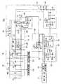
図1は、本発明の第1の実施形態に係る放電灯点灯装置の回路構成を示す図である。この図において、放電灯点灯装置10aは、一対の予熱電極(フィラメント)F1、F2を有する放電灯12に供給される印加電圧を調整することにより調光可能にすると共に、放電灯12の予熱期間(先行予熱期間)が終了した後に点灯状態への移行が容易になるように高い始動電圧を印加する始動期間を経て点灯状態に移行させるようにしたものであり、交流電圧を直流電圧に変換する直流電源14と、直流電源14の出力端に接続されたインバータ回路16と、インバータ回路16の出力端に接続され、一対の予熱電極F1、F2を予熱する予熱回路18と、インバータ回路16の出力端に接続され、放電灯12に供給する電力を調整する共振回路20とを備えている。  FIG. 1 is a diagram showing a circuit configuration of a discharge lamp lighting device according to a first embodiment of the present invention. In this figure, the dischargelamp lighting device 10a enables dimming by adjusting the applied voltage supplied to thedischarge lamp 12 having a pair of preheating electrodes (filaments) F1 and F2, and the preheating period of thedischarge lamp 12 The transition to the lighting state is made through a starting period in which a high starting voltage is applied so that the transition to the lighting state is facilitated after the (preceding preheating period) is completed, and the AC voltage is converted into a DC voltage.DC power supply 14,inverter circuit 16 connected to the output terminal ofDC power supply 14, preheatingcircuit 18 connected to the output terminal ofinverter circuit 16 to preheat the pair of preheatingelectrodes F 1 andF 2, and output ofinverter circuit 16 And aresonance circuit 20 that is connected to the end and adjusts the power supplied to thedischarge lamp 12.

また、放電灯点灯装置10aは、放電灯12に流れるランプ電流を検出するランプ電流検出回路22と、放電灯12を調光する調光器24と、調光器24の出力端に接続された直流変換回路(Duty−DC変換回路)26と、ランプ電流検出回路22から出力される検出信号と直流変換回路26から出力される指令信号とから調光制御信号を得るフィードバック回路28と、直流変換回路26から出力される指令信号を調光器24により設定された値よりも低い値から当該設定された値にスイープさせる信号昇圧回路30と、フィードバック回路28から出力される調光制御信号に基づいてインバータ回路16の動作を制御する点灯制御回路(インバータ制御回路)32とを備えている。  The dischargelamp lighting device 10 a is connected to a lampcurrent detection circuit 22 that detects a lamp current flowing through thedischarge lamp 12, a dimmer 24 that dimmes thedischarge lamp 12, and an output terminal of the dimmer 24. A DC conversion circuit (Duty-DC conversion circuit) 26, afeedback circuit 28 for obtaining a dimming control signal from a detection signal output from the lampcurrent detection circuit 22 and a command signal output from theDC conversion circuit 26; Based on asignal booster circuit 30 for sweeping a command signal output from thecircuit 26 from a value lower than the value set by the dimmer 24 to the set value, and a dimming control signal output from thefeedback circuit 28 And a lighting control circuit (inverter control circuit) 32 for controlling the operation of theinverter circuit 16.

直流電源14は、昇圧チョッパからなるものであり、交流電源VSから出力される交流電圧を全波整流することで直流電圧を得るダイオードブリッジDB1と、一端がダイオードブリッジDB1の出力端に接続されたインダクタL1と、インダクタL1の他端とグランド電位との間に接続され、インダクタL1に所定周期で電流を流すMOSFETからなるスイッチング素子Q1と、インダクタL1の他端にアノードが接続されたダイオードD1と、ダイオードD1のカソードとグランド電位との間に接続され、インダクタL1に蓄積された磁気エネルギをダイオードD1を介して蓄積するコンデンサC1と、スイッチング素子Q1の導通状態を制御する導通制御回路CCとから構成されたものである。  TheDC power source 14 is composed of a step-up chopper, and has a diode bridge DB1 that obtains a DC voltage by full-wave rectifying the AC voltage output from the AC power source VS, and one end connected to the output end of the diode bridge DB1. An inductor L1, a switching element Q1 connected between the other end of the inductor L1 and the ground potential, and passing a current through the inductor L1 in a predetermined cycle; a diode D1 having an anode connected to the other end of the inductor L1; A capacitor C1 connected between the cathode of the diode D1 and the ground potential and storing the magnetic energy stored in the inductor L1 via the diode D1, and a conduction control circuit CC for controlling the conduction state of the switching element Q1. It is configured.

インバータ回路16は、直流電源14から出力される直流電圧を高周波電圧に変換し、その変換した高周波電圧を放電灯12に供給するものであり、ダイオードD1のカソードとグランド電位との間において互いに直列接続されたMOSFETからなる2つのスイッチング素子Q2、Q3と、この2つのスイッチング素子Q2、Q3の中点に一端が接続された直流カットコンデンサC2とを含んで構成されたものである。  Theinverter circuit 16 converts a DC voltage output from theDC power source 14 into a high frequency voltage, and supplies the converted high frequency voltage to thedischarge lamp 12. Theinverter circuit 16 is connected in series between the cathode of the diode D1 and the ground potential. It is configured to include two switching elements Q2 and Q3 made of connected MOSFETs and a DC cut capacitor C2 having one end connected to the midpoint of the two switching elements Q2 and Q3.

予熱回路18は、2つの二次巻線を有する予熱トランスPTを用いた巻線予熱方式を採用したもので、一次巻線LM1がインバータ回路16の直流カットコンデンサC2の他端とグランド電位との間に接続されると共に、一方の二次巻線LM2が放電灯12の一方の予熱電極F1の両端に接続され、他方の二次巻線LM3が放電灯12の他方の予熱電極F2の両端に接続されて構成されたものである。  The preheatingcircuit 18 employs a winding preheating method using a preheating transformer PT having two secondary windings, and the primary winding LM1 is connected between the other end of the DC cut capacitor C2 of theinverter circuit 16 and the ground potential. One secondary winding LM2 is connected to both ends of one preheating electrode F1 of thedischarge lamp 12, and the other secondary winding LM3 is connected to both ends of the other preheating electrode F2 of thedischarge lamp 12. Connected and configured.

共振回路20は、一端がインバータ回路16の直流カットコンデンサC2の他端に接続されると共に、他端が放電灯12の一方の予熱電極F1に接続されたインダクタL2と、インダクタL2の他端とグランド電位との間に接続されたコンデンサC3とで構成されたものである。  Theresonance circuit 20 has one end connected to the other end of the DC cut capacitor C2 of theinverter circuit 16 and the other end connected to one preheating electrode F1 of thedischarge lamp 12, and the other end of the inductor L2. The capacitor C3 is connected to the ground potential.

ランプ電流検出回路22は、放電灯12の一対の予熱電極F1、F2間に流れるランプ電流を直流電圧に変換して検出するものであり、インバータ回路16の放電灯12に対する電力供給回路に一次巻線LM1が介挿されてなるカレントトランスCTと、カレントトランスCTの二次巻線LM2に接続され、二次巻線LM2に誘起される高周波電圧を全波整流することで直流電圧を得るダイオードブリッジDB2と、ダイオードブリッジDB2に接続された検出端を構成する抵抗素子R1とから構成されたものである。  The lampcurrent detection circuit 22 detects the lamp current flowing between the pair of preheating electrodes F1 and F2 of thedischarge lamp 12 by converting it into a DC voltage, and is used as a primary winding for the power supply circuit for thedischarge lamp 12 of theinverter circuit 16. A current transformer CT in which the line LM1 is inserted, and a diode bridge that is connected to the secondary winding LM2 of the current transformer CT and obtains a DC voltage by full-wave rectifying the high-frequency voltage induced in the secondary winding LM2. This is composed of DB2 and a resistance element R1 constituting the detection end connected to the diode bridge DB2.

このように構成されたランプ電流検出回路22では、放電灯12の予熱期間における一対の予熱電極F1、F2間にはアーク放電によるランプ電流が流れないので、抵抗素子R1の両端に電圧が出力されることはないが、放電灯12の予熱期間が終了して始動期間に達することで点灯が開始されると、一次巻線LM1にランプ電流が流れ始めることで二次巻線LM2に電圧が誘起され、この二次巻線LM2に誘起された電圧がダイオードブリッジDB2で整流されて抵抗素子R1の両端に出力される。すなわち、ランプ電流検出回路22は、放電灯12の予熱期間にはローレベルの信号を出力し、始動期間に達するとハイレベルの信号を出力する。  In the lampcurrent detection circuit 22 configured in this way, since a lamp current due to arc discharge does not flow between the pair of preheating electrodes F1 and F2 during the preheating period of thedischarge lamp 12, a voltage is output to both ends of the resistance element R1. However, when lighting starts when the preheating period of thedischarge lamp 12 ends and reaches the starting period, a voltage is induced in the secondary winding LM2 by starting the lamp current to flow in the primary winding LM1. The voltage induced in the secondary winding LM2 is rectified by the diode bridge DB2 and output to both ends of the resistance element R1. That is, the lampcurrent detection circuit 22 outputs a low level signal during the preheating period of thedischarge lamp 12, and outputs a high level signal when the start period is reached.

調光器24は、調光信号としてパルス幅変調により生成されるパルス信号を出力するものであり、デューティ比が大きくなるほど放電灯12の光出力が高光束となるようにし、デューティ比が小さくなるほど放電灯12の光出力が低光束となるようにするものである。直流変換回路26は、調光器24から出力された調光信号をデューティ比に対応したレベルの直流信号に変換するものである。すなわち、直流変換回路26は、調光器24から出力される調光信号のデューティ比が大きくなるほどハイレベルの直流信号を出力し、デューティ比が小さくなるほどローレベルの直流信号を出力する。この直流変換回路26から出力される直流信号は、調光動作を制御する指令信号としてフィードバック回路28に供給される。  The dimmer 24 outputs a pulse signal generated by pulse width modulation as a dimming signal. The light output of thedischarge lamp 12 becomes a higher luminous flux as the duty ratio increases, and the duty ratio decreases. The light output of thedischarge lamp 12 is set to a low luminous flux. TheDC conversion circuit 26 converts the dimming signal output from the dimmer 24 into a DC signal having a level corresponding to the duty ratio. That is, theDC conversion circuit 26 outputs a high-level DC signal as the duty ratio of the dimming signal output from the dimmer 24 increases, and outputs a low-level DC signal as the duty ratio decreases. The DC signal output from theDC conversion circuit 26 is supplied to thefeedback circuit 28 as a command signal for controlling the dimming operation.

フィードバック回路28は、ランプ電流検出回路22から出力される検出信号と直流変換回路26から出力される指令信号との誤差を増幅して調光制御信号として出力する誤差増幅回路を構成するオペアンプOP1を含んで構成されたもので、ランプ電流検出回路22から出力される検出信号が反転入力端子(−端子)に抵抗素子R−を介して入力され、直流変換回路26から出力される指令信号が非反転入力端子(+端子)に抵抗素子R+を介して入力される。  Thefeedback circuit 28 amplifies an error between the detection signal output from the lampcurrent detection circuit 22 and the command signal output from theDC conversion circuit 26 and outputs an operational amplifier OP1 constituting an error amplification circuit that outputs the light as a dimming control signal. The detection signal output from the lampcurrent detection circuit 22 is input to the inverting input terminal (− terminal) via the resistance element R−, and the command signal output from theDC conversion circuit 26 is not. The signal is input to the inverting input terminal (+ terminal) via the resistance element R +.

このよう構成されたフィードバック回路28は、ランプ電流検出回路22から出力される検出信号が放電灯12の予熱期間であることでローレベルにある場合には、オペアンプOP1から出力される調光制御信号は最大値に設定された状態で固定され、オペアンプOP1の動作がマスクされた状態となる。そして、放電灯12の始動期間に達すると点灯が開始されてランプ電流検出回路22から出力される検出信号がハイレベルとなり、マスクが解除されてオペアンプOP1が動作することでフィードバック回路28が機能し、出力される調光制御信号に基づいて点灯制御回路32が動作する。なお、オペアンプOP1の反転入力端子と出力端子との間には、カットオフ周波数を決定する抵抗素子RpとコンデンサCpとの並列回路が接続されており、低周波のリップルが低減されるようになっている。  When the detection signal output from the lampcurrent detection circuit 22 is at a low level due to the preheating period of thedischarge lamp 12, thefeedback circuit 28 configured in this way is a dimming control signal output from the operational amplifier OP1. Is fixed in the state set to the maximum value, and the operation of the operational amplifier OP1 is masked. When the start-up period of thedischarge lamp 12 is reached, lighting is started and the detection signal output from the lampcurrent detection circuit 22 becomes a high level, the mask is released, and the operational amplifier OP1 operates to operate thefeedback circuit 28. Thelighting control circuit 32 operates based on the output dimming control signal. Note that a parallel circuit of a resistance element Rp and a capacitor Cp for determining a cut-off frequency is connected between the inverting input terminal and the output terminal of the operational amplifier OP1, so that low-frequency ripple is reduced. ing.

信号昇圧回路30は、放電灯12の予熱期間及び始動期間に直流変換回路26から出力される指令信号を調光器24による調光可能範囲の下限値近傍レベル(下限値よりも低い値を含む。以下同じ。)に設定する電圧変更回路34と、放電灯12の予熱期間及び始動期間終了後に電圧変更回路34の動作が解除されることで直流変換回路26から出力される指令信号を調光器24で設定されたレベルにまでスイープ(徐々に復帰)させる時定数回路36と、直流変換回路26から出力される指令信号が所定のレベル以下にならないようにするリミッタ回路38とから構成されている。  Thesignal booster circuit 30 outputs a command signal output from theDC conversion circuit 26 during the preheating period and the starting period of thedischarge lamp 12 to a level near the lower limit value of a dimmable range by the dimmer 24 (including a value lower than the lower limit value) The same applies to the following), and the command signal output from theDC conversion circuit 26 is dimmed when the operation of thevoltage changing circuit 34 is canceled after the preheating period and the starting period of thedischarge lamp 12 are completed. A timeconstant circuit 36 for sweeping (gradually returning) to a level set by thedevice 24, and alimiter circuit 38 for preventing the command signal output from theDC conversion circuit 26 from falling below a predetermined level. Yes.

ここで、電圧変更回路34は、直流変換回路26の出力ラインに一端が接続された抵抗素子R2と、この抵抗素子R2の他端とグランド電位との間に接続されたスイッチ素子であるNPN型トランジスタTr1とで構成されている。このトランジスタTr1は、放電灯12の予熱期間及び始動期間に点灯制御回路32から制御端子であるベースにハイ信号が供給されることでオンし、直流変換回路26から出力される指令信号を調光器24により設定される調光可能範囲の下限値近傍レベルに設定する。  Here, thevoltage changing circuit 34 is an NPN type which is a resistance element R2 having one end connected to the output line of theDC conversion circuit 26 and a switching element connected between the other end of the resistance element R2 and the ground potential. It is composed of a transistor Tr1. The transistor Tr1 is turned on when a high signal is supplied from thelighting control circuit 32 to the base which is a control terminal during the preheating period and the starting period of thedischarge lamp 12, and the command signal output from theDC conversion circuit 26 is dimmed. The level near the lower limit value of the dimmable range set by thedevice 24 is set.

また、時定数回路36は、抵抗素子R3とコンデンサC4との直列回路により構成され、直流変換回路26の出力ラインとグランド電位との間に接続されたものである。また、リミッタ回路38は、オペアンプOP2を含んで構成されたもので、降圧した交流電圧を整流して得た電源電圧Vccを抵抗素子R4と抵抗素子R5とで分圧して得た基準電圧がオペアンプOP2の非反転入力端子(+)に入力されると共に、オペアンプOP2の出力信号がダイオードD2を介して反転入力端子(−)に入力され、オペアンプOP2の出力端がダイオードD2を介して直流変換回路26の出力ラインに接続されるようにしたものである。  The timeconstant circuit 36 is constituted by a series circuit of a resistance element R3 and a capacitor C4, and is connected between the output line of theDC conversion circuit 26 and the ground potential. Thelimiter circuit 38 includes an operational amplifier OP2, and a reference voltage obtained by dividing the power supply voltage Vcc obtained by rectifying the stepped-down AC voltage using the resistance element R4 and the resistance element R5 is an operational amplifier. While being input to the non-inverting input terminal (+) of OP2, the output signal of the operational amplifier OP2 is input to the inverting input terminal (−) via the diode D2, and the output terminal of the operational amplifier OP2 is connected to the DC conversion circuit via the diode D2. 26 output lines are connected.

点灯制御回路32は、例えばPWM−ICにより構成されたもので、放電灯12の予熱期間、始動期間及び点灯期間にインバータ回路16の動作周波数を各期間の対応する周波数に切り替える動作を行うものである。すなわち、放電灯12の予熱期間においては最も高い周波数fpreでインバータ回路16を駆動させ、始動期間においては周波数fpreよりも低い周波数fstrでインバータ回路16を駆動させ、点灯期間には周波数fstrよりも低い周波数foscでインバータ回路16を駆動させる。  Thelighting control circuit 32 is configured by, for example, a PWM-IC, and performs an operation of switching the operating frequency of theinverter circuit 16 to a frequency corresponding to each period during a preheating period, a starting period, and a lighting period of thedischarge lamp 12. is there. That is, theinverter circuit 16 is driven at the highest frequency fpre during the preheating period of thedischarge lamp 12, theinverter circuit 16 is driven at the frequency fstr lower than the frequency fpre during the start period, and is lower than the frequency fstr during the lighting period. Theinverter circuit 16 is driven at the frequency fosc.

また、点灯制御回路32は、放電灯12の予熱期間及び始動期間に電圧変更回路34のトランジスタTr1のベースにハイ信号を供給すると共に、始動期間終了後にトランジスタTr1のベースにロー信号を供給する一方、フィードバック回路28から出力される調光制御信号が増加するとインバータ回路16の動作周波数を低下させて光出力(ランプ電流)を増加させると共に、調光制御信号が減少するとインバータ回路16の動作周波数を増加させて光出力(ランプ電流)を減少させる。これにより、点灯制御回路32は、始動期間終了後にフィードバック回路28から出力される調光制御信号に基づいて放電灯12に対しフェードイン始動を行うことが可能となる。  Thelighting control circuit 32 supplies a high signal to the base of the transistor Tr1 of thevoltage changing circuit 34 during the preheating period and the starting period of thedischarge lamp 12, and supplies a low signal to the base of the transistor Tr1 after the starting period ends. When the dimming control signal output from thefeedback circuit 28 increases, the operating frequency of theinverter circuit 16 is decreased to increase the light output (lamp current), and when the dimming control signal decreases, the operating frequency of theinverter circuit 16 is increased. Increase to decrease light output (lamp current). Thereby, thelighting control circuit 32 can perform the fade-in start for thedischarge lamp 12 based on the dimming control signal output from thefeedback circuit 28 after the start period ends.

このように構成された放電灯点灯装置10aは、次のように動作する。すなわち、オペレータにより調光器24が所定の調光値に設定され、図略の電源スイッチがオンにされると、点灯制御回路32によりインバータ回路16が周波数fpreで駆動される。これにより、インバータ回路16から出力された高周波電圧が予熱回路18の予熱トランスPTの一次巻線LM1に供給され、各二次巻線LM2、LM3から予熱電極F1、F2に電圧が供給されることで各予熱電極F1、F2が予熱(先行予熱)される。  The dischargelamp lighting device 10a configured as described above operates as follows. That is, when the dimmer 24 is set to a predetermined dimming value by an operator and a power switch (not shown) is turned on, thelighting control circuit 32 drives theinverter circuit 16 at the frequency fpre. Thereby, the high-frequency voltage output from theinverter circuit 16 is supplied to the primary winding LM1 of the preheating transformer PT of the preheatingcircuit 18, and the voltage is supplied from the secondary windings LM2 and LM3 to the preheating electrodes F1 and F2. Thus, each preheating electrode F1, F2 is preheated (preceding preheating).

この予熱期間においては、放電灯12の一対の予熱電極F1、F2間にはランプ電流が流れないことからランプ電流検出回路22からの出力はローレベルになることで、フィードバック回路28から出力される調光制御信号は最大値に固定され、オペアンプOP1の動作がマスクされた状態となる。一方、予熱期間及び始動期間においては、点灯制御回路32から出力されるハイ信号により電圧変更回路34のトランジスタTr1がオンにされることで、信号昇圧回路30から出力される指令信号は調光器24による調光可能範囲の下限値近傍レベルに設定されている。これにより、点灯制御回路32は、予熱期間及び始動期間において、予め設定された所定の周波数fpre及び周波数fstrでインバータ回路16を駆動することが可能となる。  During this preheating period, since the lamp current does not flow between the pair of preheating electrodes F1 and F2 of thedischarge lamp 12, the output from the lampcurrent detection circuit 22 becomes low level and is output from thefeedback circuit 28. The dimming control signal is fixed at the maximum value, and the operation of the operational amplifier OP1 is masked. On the other hand, in the preheating period and the starting period, the transistor Tr1 of thevoltage changing circuit 34 is turned on by the high signal output from thelighting control circuit 32, so that the command signal output from thesignal booster circuit 30 is dimmer. 24 is set near the lower limit value of the dimmable range. Thus, thelighting control circuit 32 can drive theinverter circuit 16 at a predetermined frequency fpre and frequency fstr set in advance during the preheating period and the starting period.

そして、放電灯12の始動期間が終了すると、点灯制御回路32から電圧変更回路34に対して出力されているハイ信号がロー信号に変わることで電圧変更回路34のトランジスタTr1がオフになる結果、直流変換回路26から出力される指令信号は調光器24による調光可能範囲の下限値近傍レベルから調光器24により設定されたレベルにまで時定数回路36の時定数でスイープすることになる。  When the start-up period of thedischarge lamp 12 ends, the high signal output from thelighting control circuit 32 to thevoltage change circuit 34 is changed to a low signal, so that the transistor Tr1 of thevoltage change circuit 34 is turned off. The command signal output from theDC conversion circuit 26 is swept with the time constant of the timeconstant circuit 36 from the level near the lower limit value of the dimmable range by the dimmer 24 to the level set by the dimmer 24. .

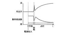
すなわち、放電灯12の始動期間が終了すると点灯制御回路32は周波数foscでインバータ回路16を駆動させようとするが、放電灯12の点灯期間になるとフィードバック回路28から出力される調光制御信号が時定数回路36の時定数に基づいてスイープする指令信号に対応して変化することで、インバータ回路16の動作周波数と光出力との関係を表わす図2及び図3に示すように、調光器24で如何なる調光レベルに設定されていたとしても、始動期間終了後において明から暗への急激な変化のない演出用途に適したフェードイン始動が行われることになる。  That is, when the start-up period of thedischarge lamp 12 ends, thelighting control circuit 32 tries to drive theinverter circuit 16 at the frequency fosc. However, when thedischarge lamp 12 enters the lighting period, the dimming control signal output from thefeedback circuit 28 is As shown in FIG. 2 and FIG. 3 showing the relationship between the operating frequency of theinverter circuit 16 and the optical output by changing in response to the command signal to be swept based on the time constant of the timeconstant circuit 36, the dimmer Whatever dimming level is set at 24, a fade-in start suitable for a production application without a sudden change from light to dark after the start period ends.

ここで、図2は始動期間が短くなるように設定した場合のインバータ回路16の動作周波数と光出力との関係を示すもので、始動期間が短いために指令信号は始動期間に達した後にすぐに調光器24で設定されたレベルにまでスイープする。図3は始動期間が長くなるように設定した場合のインバータ回路16の動作周波数と光出力との関係を示すもので、指令信号は始動後のしばらくの期間は低い値で一定となり、始動期間終了後に調光器24で設定されたレベルにまでスイープする。  Here, FIG. 2 shows the relationship between the operating frequency of theinverter circuit 16 and the optical output when the start period is set to be short. Since the start period is short, the command signal is immediately after reaching the start period. To the level set by the dimmer 24. FIG. 3 shows the relationship between the operating frequency of theinverter circuit 16 and the optical output when the start period is set to be long. The command signal is constant at a low value for a while after the start, and the start period ends. Later, the light is swept to the level set by the dimmer 24.

この図2及び図3において、いずれも予熱期間が終了して始動期間に移行したときにインバータ回路16の動作周波数が低くなることで高電圧が印加され、放電灯12が点灯して光出力が増大することになるが、この放電灯12の点灯によりランプ電流が検出されてフィードバック回路28から出力される調光制御信号が小さくなる結果、点灯制御回路32によりインバータ回路16の動作周波数が増大されて光出力が減少される。このため、このフィードバック回路28の時定数を小さくする(遅延時間を短くする)ことで、始動期間に移行したときの光出力の変化する期間(先鋭状となる期間)を短くすることができ、これにより人の目に閃光として認識できないレベルに抑えることが可能となる。  2 and 3, in both cases, when the preheating period is over and the start period is started, the operating frequency of theinverter circuit 16 is lowered so that a high voltage is applied, thedischarge lamp 12 is turned on, and the light output is generated. However, thelighting control circuit 32 increases the operating frequency of theinverter circuit 16 as a result of the lamp current being detected by the lighting of thedischarge lamp 12 and the dimming control signal output from thefeedback circuit 28 being reduced. The light output is reduced. For this reason, by reducing the time constant of the feedback circuit 28 (decreasing the delay time), it is possible to shorten the period during which the optical output changes when the start period starts (a period in which the light output changes), As a result, it is possible to suppress to a level that cannot be recognized as a flash by human eyes.

なお、調光下限値におけるインバータ回路16の動作周波数と始動時におけるインバータ回路16の動作周波数とを等しくすることで、始動期間に移行したときの閃光をより抑制することが可能になる。  In addition, by making the operating frequency of theinverter circuit 16 at the dimming lower limit value equal to the operating frequency of theinverter circuit 16 at the time of starting, it becomes possible to further suppress the flashing when shifting to the starting period.

また、本実施形態におけるフェードイン時の指令信号の変化は、図4に示すように、フェードイン開始から1秒以内に終了するように設定されている。これは、点灯後の光出力の変化に必要以上の遅れを生じさせると違和感が生じるためである。また、本実施形態では、指令信号の変化をRC時定数により実現していることから、図4に示す上向きに膨らむフェードカーブとなるが、図5に示す下向きに膨らんだフェードカーブとしてもよい。人間の目には図5に示す下向きに膨らんだフェードカーブの方がより快適に感じることができる。  Further, the change in the command signal at the time of fade-in in the present embodiment is set to end within one second from the start of the fade-in as shown in FIG. This is because a sense of incongruity occurs when a delay more than necessary is caused in the change in the light output after lighting. Further, in the present embodiment, since the change of the command signal is realized by the RC time constant, the fade curve bulges upward as shown in FIG. 4, but it may be a fade curve bulges downward as shown in FIG. The fading curve bulging downward shown in FIG. 5 can be more comfortably felt by human eyes.

図6は、本発明の第2の実施形態に係る放電灯点灯装置の回路構成を示す図である。この第2の実施形態に係る回路構成では、図1に示す第1の実施形態に係る回路構成と基本的には同一の構成要素からなるものであるため、同一の機能を有する構成要素については同一の符号を付与することにより詳細な説明を省略し、以下には第1の実施形態に係る回路構成との相違点を中心に説明する。この第2の実施形態に係る回路構成は、第1の実施形態に係る回路構成とは、放電灯12の始動期間に放電灯12が点灯したか否かを判別する点灯判別回路40を備え、この点灯判別回路40からの出力信号により信号昇圧回路30の電圧変更回路34の動作を制御するようにした点で相違するものであり、その他の構成は第1の実施形態に係るものと同一である。  FIG. 6 is a diagram showing a circuit configuration of a discharge lamp lighting device according to the second embodiment of the present invention. The circuit configuration according to the second embodiment is basically composed of the same components as the circuit configuration according to the first embodiment shown in FIG. Detailed description will be omitted by assigning the same reference numerals, and the following description will focus on differences from the circuit configuration according to the first embodiment. The circuit configuration according to the second embodiment is different from the circuit configuration according to the first embodiment in that it includes alighting determination circuit 40 that determines whether or not thedischarge lamp 12 is lit during the starting period of thedischarge lamp 12, The difference is that the operation of thevoltage changing circuit 34 of thesignal booster circuit 30 is controlled by the output signal from thelighting discrimination circuit 40, and the other configurations are the same as those according to the first embodiment. is there.

すなわち、この第2の実施形態に係る放電灯点灯装置10bは、点灯判別回路40がコンパレータCP1を含んで構成されたものであり、ランプ電流検出回路22から出力される検出信号がコンパレータCP1の反転入力端子(−端子)に入力されると共に、降圧した交流電圧を整流して得た電源電圧Vccを抵抗素子R6及びR7により分圧して得た基準電圧がコンパレータCP1の非反転入力端子(+端子)に入力され、コンパレータCP1の出力端子から出力される検出信号が電圧変更回路34のトランジスタTr1のベースに入力されるようにしたものである。なお、ランプ電流検出回路22から出力される検出信号が入力される入力端子とグランド電位との間に入力値を安定化するための充電用のコンデンサC5が接続されている。  That is, in the dischargelamp lighting device 10b according to the second embodiment, thelighting determination circuit 40 includes the comparator CP1, and the detection signal output from the lampcurrent detection circuit 22 is inverted from the comparator CP1. The reference voltage obtained by dividing the power supply voltage Vcc obtained by rectifying the stepped-down AC voltage with the resistance elements R6 and R7 is input to the input terminal (−terminal), and the non-inverting input terminal (+ terminal) of the comparator CP1 ) And the detection signal output from the output terminal of the comparator CP1 is input to the base of the transistor Tr1 of thevoltage changing circuit 34. A charging capacitor C5 for stabilizing the input value is connected between the input terminal to which the detection signal output from the lampcurrent detection circuit 22 is input and the ground potential.

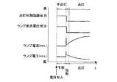
このように構成された第2の実施形態に係る放電灯点灯装置10bは、光出力、インバータ回路16の動作周波数及び点灯判別回路40の出力が図7に示すような関係性を呈するように動作する。すなわち、放電灯12の予熱期間においてはランプ電流が流れないことでランプ電流検出回路22からの検出信号はローレベルとなり、コンパレータCP1の出力端子からハイ信号が出力される。このため、電圧変更回路34のトランジスタTr1がオンにされることで、信号昇圧回路30から出力される指令信号は調光器24による調光可能範囲の下限値近傍レベルに設定される。  The dischargelamp lighting device 10b according to the second embodiment configured as described above operates such that the light output, the operating frequency of theinverter circuit 16, and the output of thelighting determination circuit 40 exhibit the relationship as shown in FIG. To do. That is, since the lamp current does not flow during the preheating period of thedischarge lamp 12, the detection signal from the lampcurrent detection circuit 22 becomes low level, and a high signal is output from the output terminal of the comparator CP1. Therefore, when the transistor Tr1 of thevoltage changing circuit 34 is turned on, the command signal output from thesignal booster circuit 30 is set to a level near the lower limit value of the dimmable range by the dimmer 24.

ところが、予熱期間が終了して始動期間に達するとランプ電流が流れることでランプ電流検出回路22から出力される検出信号がハイレベルとなり、コンパレータCP1の出力端子からはロー信号が出力される。このため、電圧変更回路34のトランジスタTr1がオフにされることで、信号昇圧回路30から出力される指令信号は調光器24による調光可能範囲の下限値近傍レベルから調光器24により設定されたレベルにまで時定数回路36の時定数でスイープすることになり、フィードバック回路28の調光制御信号に応じてインバータ回路16の動作周波数が徐々に低下することで放電灯12の光出力が漸次増加していくことになる。  However, when the preheating period ends and the starting period is reached, the lamp current flows, so that the detection signal output from the lampcurrent detection circuit 22 becomes a high level, and a low signal is output from the output terminal of the comparator CP1. Therefore, when the transistor Tr1 of thevoltage changing circuit 34 is turned off, the command signal output from thesignal booster circuit 30 is set by the dimmer 24 from the level near the lower limit value of the dimmable range by the dimmer 24. The time constant of the timeconstant circuit 36 is swept up to the set level, and the operating frequency of theinverter circuit 16 gradually decreases in accordance with the dimming control signal of thefeedback circuit 28, so that the light output of thedischarge lamp 12 is increased. It will gradually increase.

このように構成された第2の実施形態に係る放電灯点灯装置10bにおいては、第1の実施形態に係る放電灯点灯装置10aにおいて奏する作用効果に加え、次のような作用効果を奏する。すなわち、点灯判別回路40により電圧変更回路34の動作を制御しているので、放電灯12の始動期間内にフェードイン始動を開始することができるようになり、第1の実施形態に係る放電灯点灯装置10aに比べて十分な始動期間を設定することができることから、低温時においても放電灯12の始動性を向上させることができる。  The dischargelamp lighting device 10b according to the second embodiment configured as described above has the following effects in addition to the effects provided by the dischargelamp lighting device 10a according to the first embodiment. In other words, since the operation of thevoltage change circuit 34 is controlled by thelighting determination circuit 40, the fade-in start can be started within the start-up period of thedischarge lamp 12, and the discharge lamp according to the first embodiment. Since a sufficient starting period can be set as compared with thelighting device 10a, the startability of thedischarge lamp 12 can be improved even at a low temperature.

また、始動期間を長く設定しても始動直後から始動期間の終了までの間に光出力が一定になることがないので、フェードイン時の明暗の差による違和感がより改善されることになると共に、始動期間内にフェードイン始動が開始されることで低温時に発生しやすくなる始動直後の光のジャンプ現象が発生し難くなるという利点もある。なお、ここでいうジャンプ現象とは、放電灯12がアーク放電からグロー放電に移行し、放電灯12の管端のみが僅かに光る現象をいう。  In addition, even if the start period is set longer, the light output does not become constant from immediately after the start to the end of the start period, so that the sense of incongruity due to the difference in brightness during fade-in is further improved. In addition, since the fade-in start is started within the start period, there is also an advantage that the light jump phenomenon immediately after the start, which is likely to occur at a low temperature, is difficult to occur. The jump phenomenon here refers to a phenomenon in which thedischarge lamp 12 shifts from arc discharge to glow discharge, and only the tube end of thedischarge lamp 12 shines slightly.

図8は、本発明の第3の実施形態に係る放電灯点灯装置の回路構成を示す図である。この第3の実施形態に係る回路構成では、図6に示す第2の実施形態に係る回路構成と基本的には同一の構成要素からなるものであるため、同一の機能を有する構成要素については同一の符号を付与することにより詳細な説明を省略し、以下には第2の実施形態に係る回路構成との相違点を中心に説明する。この第3の実施形態に係る回路構成は、第2の実施形態に係る回路構成とは、放電灯12の始動期間に放電灯12が点灯したか否かを判別する点灯判別回路40が放電灯12に印加される直流電圧成分を検出するように構成された点で相違するものであり、その他の構成は第2の実施形態に係るものと同一である。  FIG. 8 is a diagram showing a circuit configuration of a discharge lamp lighting device according to the third embodiment of the present invention. The circuit configuration according to the third embodiment is basically composed of the same components as the circuit configuration according to the second embodiment shown in FIG. Detailed description will be omitted by assigning the same reference numerals, and the following description will focus on differences from the circuit configuration according to the second embodiment. The circuit configuration according to the third embodiment is different from the circuit configuration according to the second embodiment in that thelighting determination circuit 40 that determines whether or not thedischarge lamp 12 is lit during the starting period of thedischarge lamp 12 12 is different from that of the second embodiment in that it is configured to detect a direct-current voltage component applied to the first and second embodiments.

すなわち、この第3の実施形態に係る放電灯点灯装置10cは、点灯判別回路40がコンパレータCP1を含むと共に、直流電源14から放電灯12に供給される直流電圧成分を検出するための電圧検出回路42を備えて構成されたものである。  That is, in the dischargelamp lighting device 10c according to the third embodiment, thelighting determination circuit 40 includes the comparator CP1, and the voltage detection circuit for detecting the DC voltage component supplied from theDC power supply 14 to thedischarge lamp 12. 42 is configured.

この電圧検出回路42は、直流電源14の高電位側の出力端と放電灯12の一方の予熱電極F1との間に接続された高抵抗の抵抗素子R11、R12及びR13の直列抵抗回路44と、一端がグランド電位に接続された充電用のコンデンサC6と、放電灯12の一方の予熱電極F1とコンデンサC6の他端に接続された高抵抗の抵抗素子R14、R15及びR16の直列抵抗回路46とを含んで構成されたもので、直列抵抗回路46とコンデンサC6との接続点がダイオードD3を介してコンパレータCP1の非反転入力端子(+端子)に接続されている。  Thisvoltage detection circuit 42 includes aseries resistance circuit 44 of high-resistance resistance elements R11, R12, and R13 connected between the output terminal on the high potential side of theDC power supply 14 and one preheating electrode F1 of thedischarge lamp 12. , A charging capacitor C6 having one end connected to the ground potential, and aseries resistance circuit 46 of high-resistance resistance elements R14, R15 and R16 connected to one preheating electrode F1 of thedischarge lamp 12 and the other end of the capacitor C6. The connection point between theseries resistance circuit 46 and the capacitor C6 is connected to the non-inverting input terminal (+ terminal) of the comparator CP1 via the diode D3.

また、コンパレータCP1の反転入力端子(−端子)には、電源電圧Vccを抵抗素子R9及びR10により分圧して得た基準電圧が入力され、コンパレータCP1の出力端子から出力される検出信号が電圧変更回路34のトランジスタTr1のベースに入力されるようになっている。なお、コンパレータCP1の非反転入力端子とグランド電位との間には、入力値を安定化するための充電用のコンデンサC7と、このコンデンサC7に充電された電荷を放電するための抵抗素子R17とが接続されている。  Further, a reference voltage obtained by dividing the power supply voltage Vcc by the resistance elements R9 and R10 is input to the inverting input terminal (− terminal) of the comparator CP1, and the detection signal output from the output terminal of the comparator CP1 is changed in voltage. The signal is input to the base of the transistor Tr1 of thecircuit 34. Between the non-inverting input terminal of the comparator CP1 and the ground potential, a charging capacitor C7 for stabilizing the input value and a resistance element R17 for discharging the charge charged in the capacitor C7 are provided. Is connected.

このように構成された第3の実施形態に係る放電灯点灯装置10cは、点灯判別回路40の出力、放電灯12の直流電圧成分、放電灯12に流れるランプ電流及び放電灯12のランプ電圧が図9に示すような関係性を呈するように動作する。すなわち、放電灯12の予熱期間においては、一対の予熱電極F1、F2間の等価抵抗は無限大であるため、直流電源14から放電灯12に重畳される直流電圧が高抵抗の直列抵抗回路44、46を介してコンデンサC6に充電され、この電位がダイオードD2を介してコンパレータCP1の非反転入力端子に入力されることで、コンパレータCP1の出力端子からハイ信号が出力される。このため、電圧変更回路34のトランジスタTr1がオンにされることで、信号昇圧回路30から出力される指令信号は調光器24による調光可能範囲の下限値近傍レベルに設定される。  In the dischargelamp lighting device 10c according to the third embodiment configured as described above, the output of thelighting determination circuit 40, the DC voltage component of thedischarge lamp 12, the lamp current flowing through thedischarge lamp 12, and the lamp voltage of thedischarge lamp 12 are It operates so as to exhibit the relationship as shown in FIG. That is, during the preheating period of thedischarge lamp 12, since the equivalent resistance between the pair of preheating electrodes F1 and F2 is infinite, the DC resistance superimposed from theDC power supply 14 to thedischarge lamp 12 is a high resistanceseries resistance circuit 44. 46, the capacitor C6 is charged, and this potential is input to the non-inverting input terminal of the comparator CP1 via the diode D2, so that a high signal is output from the output terminal of the comparator CP1. Therefore, when the transistor Tr1 of thevoltage changing circuit 34 is turned on, the command signal output from thesignal booster circuit 30 is set to a level near the lower limit value of the dimmable range by the dimmer 24.

一方、予熱期間が終了して始動期間に移行すると点灯が開始されることで放電灯12の等価抵抗が低下し、コンデンサC6には正負のバランスのとれた充放電電流が流れることで殆ど充電されないことになり、コンパレータCP1の非反転入力端子に入力される電圧はほぼゼロとなることから、コンパレータCP1の出力端子からはロー信号が出力される。このため、電圧変更回路34のトランジスタTr1がオフにされることで、信号昇圧回路30から出力される指令信号は調光器24による調光可能範囲の下限値近傍レベルから調光器24により設定されたレベルにまで時定数回路36の時定数でスイープすることになり、フィードバック回路28の調光制御信号に応じてインバータ回路16の動作周波数が徐々に低下することで放電灯12の光出力が漸次増加していくことになる。  On the other hand, when the preheating period ends and the start period starts, lighting is started to reduce the equivalent resistance of thedischarge lamp 12, and the capacitor C6 is charged with a positive / negative balanced charge / discharge current that is hardly charged. As a result, the voltage input to the non-inverting input terminal of the comparator CP1 is almost zero, so that a low signal is output from the output terminal of the comparator CP1. Therefore, when the transistor Tr1 of thevoltage changing circuit 34 is turned off, the command signal output from thesignal booster circuit 30 is set by the dimmer 24 from the level near the lower limit value of the dimmable range by the dimmer 24. The time constant of the timeconstant circuit 36 is swept up to the set level, and the operating frequency of theinverter circuit 16 gradually decreases in accordance with the dimming control signal of thefeedback circuit 28, so that the light output of thedischarge lamp 12 is increased. It will gradually increase.

このように、この第3の実施形態に係る放電灯点灯装置10cにおいては、放電灯12に印加される直流電圧成分を検出することで始動期間に放電灯12が点灯したか否かを判別する点灯判別回路40により電圧変更回路34の動作を制御しているので、第2の実施形態の場合と同様に始動期間内にフェードイン始動を開始することができるようになり、第1の実施形態に係る放電灯点灯装置10aに比べて十分な始動期間を設定することができることから、低温時においても放電灯12の始動性を向上させることができる。  Thus, in the dischargelamp lighting device 10c according to the third embodiment, it is determined whether or not thedischarge lamp 12 has been lit during the starting period by detecting the DC voltage component applied to thedischarge lamp 12. Since the operation of thevoltage change circuit 34 is controlled by thelighting determination circuit 40, the fade-in start can be started within the start period as in the case of the second embodiment. Since a sufficient starting period can be set as compared with the dischargelamp lighting device 10a according to the above, the startability of thedischarge lamp 12 can be improved even at a low temperature.

また、始動期間を長く設定しても始動直後から始動期間の終了までの間に光出力が一定になることがないので、フェードイン時の明暗の差による違和感がより改善されることになると共に、始動期間内にフェードイン始動が開始されることで低温時に発生しやすくなる始動直後の光のジャンプ現象が発生し難くなるという利点もある。  In addition, even if the start period is set longer, the light output does not become constant from immediately after the start to the end of the start period, so that the sense of incongruity due to the difference in brightness during fade-in is further improved. In addition, since the fade-in start is started within the start period, there is also an advantage that the light jump phenomenon immediately after the start, which is likely to occur at a low temperature, is difficult to occur.

また、放電灯12に供給される直流電圧成分を検出することで始動期間に放電灯12が点灯したか否かを判別するので、第2の実施形態に係る放電灯点灯装置10bのようにランプ電流により放電灯12が点灯したか否かを判別するもの比べ、放電灯12が点灯しない予熱期間における検出信号と放電灯12が点灯する始動期間における検出信号との差異が大きくなる結果、始動期間における点灯判別を確実に行うことができる。このことは、図9に示す波形図からも理解することができる。なお、放電灯12に供給される直流電圧成分を検出する構成としたことで、その検出回路をランプ寿命末期検出回路と共用することが可能となる。  In addition, since the DC voltage component supplied to thedischarge lamp 12 is detected to determine whether or not thedischarge lamp 12 has been lit during the start-up period, a lamp like the dischargelamp lighting device 10b according to the second embodiment is used. As a result of the difference between the detection signal in the preheating period in which thedischarge lamp 12 is not lit and the detection signal in the start period in which thedischarge lamp 12 is lit, compared to what determines whether or not thedischarge lamp 12 is lit by current. It is possible to reliably perform the lighting determination at. This can also be understood from the waveform diagram shown in FIG. In addition, since it is configured to detect the DC voltage component supplied to thedischarge lamp 12, the detection circuit can be shared with the lamp end-of-life detection circuit.

図10は、本発明の第4の実施形態に係る放電灯点灯装置の回路構成を示す図である。この第4の実施形態に係る回路構成では、図8に示す第3の実施形態に係る回路構成と基本的には同一の構成要素からなるものであるため、同一の機能を有する構成要素については同一の符号を付与することにより詳細な説明を省略し、以下には第3の実施形態に係る回路構成との相違点を中心に説明する。この第4の実施形態に係る回路構成は、第3の実施形態に係る回路構成とは、予熱電極F1、F2の予熱方式として一対の予熱電極F1、F2間に始動コンデンサC10を接続したC予熱方式を採用すると共に、これに伴ってランプ電流検出回路22の構成を異ならせた点で相違するものであり、その他の構成は第3の実施形態に係るものと同一である。  FIG. 10 is a diagram showing a circuit configuration of a discharge lamp lighting device according to the fourth embodiment of the present invention. The circuit configuration according to the fourth embodiment is basically composed of the same components as the circuit configuration according to the third embodiment shown in FIG. Detailed description will be omitted by assigning the same reference numerals, and the following description will focus on differences from the circuit configuration according to the third embodiment. The circuit configuration according to the fourth embodiment is different from the circuit configuration according to the third embodiment as C preheating in which a starting capacitor C10 is connected between a pair of preheating electrodes F1 and F2 as a preheating method for the preheating electrodes F1 and F2. The system is different and the configuration of the lampcurrent detection circuit 22 is changed accordingly, and the other configuration is the same as that according to the third embodiment.

すなわち、この第4の実施形態に係る放電灯点灯装置10dは、放電灯12の予熱電極F1、F2間に始動コンデンサC10を接続して構成した予熱回路50を備えると共に、一次巻線LM1、二次巻線LM2及び三次巻線LM3を備えたカレントトランスCTを用いてランプ電流検出回路22を構成したものである。このカレントトランスCTは、その一次巻線LM1がインバータ回路16から放電灯12に対して電力を供給する電力供給回路(すなわち、放電灯12の予熱電流とランプ電流とが共に流れる個所)に介挿され、二次巻線LM2が予熱回路50(すなわち、放電灯12の予熱電流のみが流れる個所)に一次巻線LM1とは逆極性(逆相)となるように介挿され、三次巻線LM3がランプ電流を検出する検出巻線となるようにされたものである。  That is, the dischargelamp lighting device 10d according to the fourth embodiment includes the preheatingcircuit 50 configured by connecting the starting capacitor C10 between the preheating electrodes F1 and F2 of thedischarge lamp 12, and the primary windings LM1 and 2 The lampcurrent detection circuit 22 is configured using a current transformer CT including a secondary winding LM2 and a tertiary winding LM3. The current transformer CT is inserted in a power supply circuit whose primary winding LM1 supplies electric power from theinverter circuit 16 to the discharge lamp 12 (that is, a place where the preheating current and the lamp current of thedischarge lamp 12 flow together). The secondary winding LM2 is inserted into the preheating circuit 50 (that is, where only the preheating current of thedischarge lamp 12 flows) so as to have a reverse polarity (reverse phase) to the primary winding LM1, and the tertiary winding LM3 Is a detection winding for detecting the lamp current.

このように構成された第4の実施形態に係る放電灯点灯装置10dは、放電灯12の予熱期間にはランプ電流が流れないことから一次巻線LM1及び二次巻線LM2に互いに逆向きの予熱電流(先行予熱電流)が流れることで磁界が打ち消され、三次巻線LM3には検出電圧が出力されないことになる。また、始動期間及び点灯期間には、一次巻線LM1に予熱電流(常時予熱電流)とランプ電流の合成電流が流れ、二次巻線LM2に予熱電流(常時予熱電流)が流れることで三次巻線LM3には予熱電流とランプ電流の合成電流から予熱電流が打ち消されたランプ電流のみによる検出電圧が検出されることになる。このため、C予熱方式を採用した場合であっても放電灯12に流れるランプ電流を正確に検出することができ、ランプ電流のフィードバック制御によるフェードイン始動を確実に行うことができる。  In the dischargelamp lighting device 10d according to the fourth embodiment configured as described above, since the lamp current does not flow during the preheating period of thedischarge lamp 12, the primary winding LM1 and the secondary winding LM2 are opposite to each other. When the preheating current (preceding preheating current) flows, the magnetic field is canceled and the detection voltage is not output to the tertiary winding LM3. Further, during the start-up period and the lighting period, a combined current of the preheating current (always preheating current) and the lamp current flows in the primary winding LM1, and the preheating current (always preheating current) flows in the secondary winding LM2, so that the tertiary winding On the line LM3, a detection voltage based only on the lamp current in which the preheating current is canceled out from the combined current of the preheating current and the lamp current is detected. For this reason, even when the C preheating method is adopted, the lamp current flowing through thedischarge lamp 12 can be accurately detected, and the fade-in start by the feedback control of the lamp current can be reliably performed.

図11は、本発明の第5の実施形態に係る放電灯点灯装置の回路構成を示す図である。この第5の実施形態に係る回路構成では、図8に示す第3の実施形態に係る回路構成と基本的には同一の構成要素からなるものであるため、同一の機能を有する構成要素については同一の符号を付与することにより詳細な説明を省略し、以下には第3の実施形態に係る回路構成との相違点を中心に説明する。この第5の実施形態に係る回路構成は、第3の実施形態に係る回路構成とは、放電灯12への電力供給を出力トランスを用いて行い、これに伴ってランプ電流検出回路22の構成を異ならせた点で相違するものであり、その他の構成は第3の実施形態に係るものと同一である。  FIG. 11 is a diagram showing a circuit configuration of a discharge lamp lighting device according to the fifth embodiment of the present invention. The circuit configuration according to the fifth embodiment is basically composed of the same components as the circuit configuration according to the third embodiment shown in FIG. Detailed description will be omitted by assigning the same reference numerals, and the following description will focus on differences from the circuit configuration according to the third embodiment. The circuit configuration according to the fifth embodiment is different from the circuit configuration according to the third embodiment in that power is supplied to thedischarge lamp 12 using an output transformer, and accordingly, the configuration of the lampcurrent detection circuit 22 is configured. And the other configurations are the same as those according to the third embodiment.

すなわち、この第5の実施形態に係る放電灯点灯装置10eは、共振回路20のコンデンサC3に並列に一次巻線LM1を接続した出力トランス(センタータップトランス)OTのセンタータップを有する二次巻線LM2の両端を一対の予熱電極F1、F2の各一端にそれぞれ接続して電力供給を行うことで放電灯12を点灯させるようにする一方、一次巻線LM1、二次巻線LM2及び三次巻線LM3を備えたカレントトランスCTを用い、その一次巻線LM1を予熱電極F2の一端とその一端に接続される予熱トランスPTの二次巻線LM2及び出力トランスOTの二次巻線LM2との間(すなわち、放電灯12の予熱電流とランプ電流とが共に流れる個所)に介挿すると共に、二次巻線LM2を予熱電極F2の他端とその他端に接続される予熱トランスPTの二次巻線LM2との間(すなわち、放電灯12の予熱電流のみが流れる個所)に一次巻線LM1とは逆極性(逆相)となるように介挿し、三次巻線LM3がランプ電流を検出する検出巻線となるようにしてランプ電流検出回路22を構成したものである。  That is, the dischargelamp lighting device 10e according to the fifth embodiment includes a secondary winding having a center tap of an output transformer (center tap transformer) OT in which the primary winding LM1 is connected in parallel to the capacitor C3 of theresonance circuit 20. While connecting the both ends of LM2 to each one end of a pair of preheating electrodes F1 and F2, and supplying power, thedischarge lamp 12 is turned on, while the primary winding LM1, the secondary winding LM2, and the tertiary winding Using a current transformer CT provided with LM3, the primary winding LM1 is connected between one end of the preheating electrode F2, the secondary winding LM2 of the preheating transformer PT connected to the one end thereof, and the secondary winding LM2 of the output transformer OT. (That is, the portion where the preheating current and the lamp current of thedischarge lamp 12 flow together) and the secondary winding LM2 is connected to the other end and the other end of the preheating electrode F2. Is inserted between the secondary winding LM2 of the preheating transformer PT (that is, where only the preheating current of thedischarge lamp 12 flows) so as to have a reverse polarity (reverse phase) with respect to the primary winding LM1. The lampcurrent detection circuit 22 is configured such that LM3 serves as a detection winding for detecting the lamp current.

このように構成された第5の実施形態に係る放電灯点灯装置10eは、放電灯12の予熱期間にはランプ電流が流れないことからカレントトランスCTの一次巻線LM1及び二次巻線LM2に互いに逆向きの予熱電流(先行予熱電流)が流れることで磁界が打ち消され、三次巻線LM3には検出電圧が出力されないことになる。また、始動期間及び点灯期間には、一次巻線LM1に予熱電流(常時予熱電流)とランプ電流の合成電流が流れ、二次巻線LM2に予熱電流(常時予熱電流)が流れることで三次巻線LM3には予熱電流とランプ電流の合成電流から予熱電流が打ち消されたランプ電流のみによる検出電圧が検出されることになる。このため、予熱トランスPTを用いた巻線予熱方式を採用すると共に、電力供給回路に出力トランスOTを用いた場合であっても放電灯12に流れるランプ電流を正確に検出することができ、ランプ電流のフィードバック制御によるフェードイン始動を確実に行うことができる。  In the dischargelamp lighting device 10e according to the fifth embodiment configured as described above, since the lamp current does not flow during the preheating period of thedischarge lamp 12, the primary winding LM1 and the secondary winding LM2 of the current transformer CT are used. The preheating currents (preceding preheating currents) that are opposite to each other flow to cancel the magnetic field, and no detection voltage is output to the tertiary winding LM3. Further, during the start-up period and the lighting period, a combined current of the preheating current (always preheating current) and the lamp current flows in the primary winding LM1, and the preheating current (always preheating current) flows in the secondary winding LM2, so that the tertiary winding On the line LM3, a detection voltage based only on the lamp current in which the preheating current is canceled out from the combined current of the preheating current and the lamp current is detected. For this reason, the winding preheating method using the preheating transformer PT is adopted, and the lamp current flowing through thedischarge lamp 12 can be accurately detected even when the output transformer OT is used in the power supply circuit. Fade-in starting by current feedback control can be performed reliably.

なお、予熱トランスPTを用いた巻線予熱方式を採用した場合は、カレントトランスCTの一次巻線LM1及び二次巻線LM2のみでランプ電流の検出は可能ではあるが、調光の下限付近における低光束時ではラインインピーダンスが非常に大きくなることからランプ電流が小さくなるにも拘わらず予熱電流が大きくなる。このため、予熱電流による漏れ電流によりランプ電流が正確に検出できないことになると共に、低温時においては実際のランプ電流と検出されるランプ電流との相関関係が変化するなどして実際のランプ電流よりも大きな値のランプ電流が検出されることになり、低光束からフェードイン始動を行うときにジャンプ現象やちらつきが生じる虞がある。これに対し、本実施形態による方式によれば、調光の下限付近における低光束時においてもランプ電流を正確に検出することができることになり、低温時においても予熱電流による漏れ電流に影響されることなくフェードイン始動を確実に行うことができる。  When the winding preheating method using the preheating transformer PT is adopted, the lamp current can be detected only by the primary winding LM1 and the secondary winding LM2 of the current transformer CT, but near the lower limit of dimming. When the luminous flux is low, the line impedance becomes very large, so that the preheating current becomes large although the lamp current becomes small. For this reason, the lamp current cannot be accurately detected due to the leakage current due to the preheating current, and the correlation between the actual lamp current and the detected lamp current changes at low temperatures. In other words, a large value of the lamp current is detected, and there is a possibility that a jump phenomenon or flicker may occur when fading-in is started from a low luminous flux. On the other hand, according to the method according to the present embodiment, the lamp current can be accurately detected even at a low light flux near the lower limit of dimming, and is affected by the leakage current due to the preheating current even at a low temperature. Thus, it is possible to reliably perform the fade-in start.

図12は、本発明の第6の実施形態に係る放電灯点灯装置の回路構成を示す図である。この第6の実施形態に係る回路構成では、図11に示す第5の実施形態に係る回路構成と基本的には同一の構成要素からなるものであるため、同一の機能を有する構成要素については同一の符号を付与することにより詳細な説明を省略し、以下には第5の実施形態に係る回路構成との相違点を中心に説明する。  FIG. 12 is a diagram showing a circuit configuration of a discharge lamp lighting device according to the sixth embodiment of the present invention. The circuit configuration according to the sixth embodiment is basically composed of the same components as the circuit configuration according to the fifth embodiment shown in FIG. Detailed description will be omitted by assigning the same reference numerals, and the following description will focus on differences from the circuit configuration according to the fifth embodiment.

すなわち、この第6の実施形態に係る放電灯点灯装置10fは、第5の実施形態に係る回路構成とは、フィードバック回路28を構成するオペアンプOP1の反転入力端子(−端子)とグランド電位間にスイッチ素子であるNPN型トランジスタTr2を接続することでマスク回路54を構成し、そのマスク回路54の制御端子となるベースに点灯制御回路32から制御信号を供給するようにした点で相違するものであり、その他の構成は第5の実施形態に係るものと同一である。なお、この第6の実施形態に係る回路構成では、直流電源14の具体的回路構成を省略して示している。また、放電灯12の電力供給回路を構成する出力トランスOTとして二次巻線LM2にセンタータップを有しないものを用いている。  That is, the dischargelamp lighting device 10f according to the sixth embodiment differs from the circuit configuration according to the fifth embodiment between the inverting input terminal (− terminal) of the operational amplifier OP1 constituting thefeedback circuit 28 and the ground potential. This is different in that amask circuit 54 is configured by connecting an NPN transistor Tr2 that is a switch element, and a control signal is supplied from thelighting control circuit 32 to a base that is a control terminal of themask circuit 54. In other respects, the configuration is the same as that according to the fifth embodiment. In the circuit configuration according to the sixth embodiment, the specific circuit configuration of theDC power supply 14 is omitted. Further, as the output transformer OT constituting the power supply circuit of thedischarge lamp 12, a secondary winding LM2 having no center tap is used.

このように構成された第6の実施形態に係る放電灯点灯装置10fは、放電灯12の予熱期間にのみ点灯制御回路32からハイ信号がマスク回路54を構成するトランジスタTr2のベースに供給されることでトランジスタTr2がオンとなり、オペアンプOP1の反転入力端子がグランド電位に接続されることになる結果、オペアンプOP1から出力される調光制御信号が予熱期間中は必ず最大値で固定され、フィードバック回路28の動作にマスク期間が設けられることになり、低温時においても確実に低光束からフェードイン始動を行うことができる。  In the dischargelamp lighting device 10f according to the sixth embodiment configured as described above, a high signal is supplied from thelighting control circuit 32 to the base of the transistor Tr2 constituting themask circuit 54 only during the preheating period of thedischarge lamp 12. As a result, the transistor Tr2 is turned on, and the inverting input terminal of the operational amplifier OP1 is connected to the ground potential. As a result, the dimming control signal output from the operational amplifier OP1 is always fixed at the maximum value during the preheating period. A mask period is provided for theoperation 28, and fading-in start can be reliably performed from a low luminous flux even at a low temperature.

すなわち、ランプ電流のフィードバック制御の場合、通常であれば放電灯12の予熱期間においてはランプ電流検出回路22で検出されるランプ電流はローレベルであるため、オペアンプOP1から出力される調光制御信号が予熱期間では最大値に固定されることになる。ところが、予熱期間における予熱電流や回路パターンを流れる電流が漏れ電流となり、この漏れ電流がランプ電流としてオペアンプOP1の反転入力端子に入力される結果、フィードバック回路28が動作してオペアンプOP1から出力される調光制御信号が予熱期間であるにも拘わらず小さくなってしまう。  That is, in the case of the lamp current feedback control, the lamp current detected by the lampcurrent detection circuit 22 is normally at a low level during the preheating period of thedischarge lamp 12, and therefore the dimming control signal output from the operational amplifier OP1. However, the maximum value is fixed during the preheating period. However, the preheating current during the preheating period and the current flowing through the circuit pattern become a leakage current, and this leakage current is input to the inverting input terminal of the operational amplifier OP1 as a lamp current. As a result, thefeedback circuit 28 operates and is output from the operational amplifier OP1. The dimming control signal becomes small despite the preheating period.

このように、調光制御信号が予熱期間であるにも拘わらず小さくなると、始動期間に移行したときに所定の始動電圧を放電灯12に供給することができないことになり、低光束からのフェードイン始動が困難となるのに対し、本実施形態に係る構成によれば、予熱期間におけるフィードバック回路28の動作にマスク期間が設けられることで確実に低光束からフェードイン始動させることができる。  In this way, if the dimming control signal becomes small in spite of the preheating period, a predetermined starting voltage cannot be supplied to thedischarge lamp 12 when the starting period is started, and fading from a low luminous flux is not possible. While in-starting is difficult, according to the configuration according to the present embodiment, the operation of thefeedback circuit 28 in the preheating period is provided with a mask period, so that fading-in start can be reliably started from a low luminous flux.

図13は、本発明の第7の実施形態に係る放電灯点灯装置の回路構成を示す図である。この第7の実施形態に係る回路構成では、図12に示す第6の実施形態に係る回路構成と基本的には同一の構成要素からなるものであるため、同一の機能を有する構成要素については同一の符号を付与することにより詳細な説明を省略し、以下には第6の実施形態に係る回路構成との相違点を中心に説明する。  FIG. 13 is a diagram showing a circuit configuration of a discharge lamp lighting device according to the seventh embodiment of the present invention. Since the circuit configuration according to the seventh embodiment is basically composed of the same components as the circuit configuration according to the sixth embodiment shown in FIG. 12, the components having the same functions are as follows. Detailed description will be omitted by assigning the same reference numerals, and the following description will focus on differences from the circuit configuration according to the sixth embodiment.

すなわち、この第7の実施形態に係る放電灯点灯装置10gは、第6の実施形態に係る回路構成とは、フィードバック回路28におけるオペアンプOP1の反転入力端子(−端子)とグランド電位間に設けたマスク回路54を構成するトランジスタTr2の制御を点灯判別回路40のコンパレータCP1の出力信号により行うようにした点で相違するものであり、その他の構成は第6の実施形態に係るものと同一である。  That is, the dischargelamp lighting device 10g according to the seventh embodiment is provided between the inverting input terminal (−terminal) of the operational amplifier OP1 in thefeedback circuit 28 and the ground potential, unlike the circuit configuration according to the sixth embodiment. The difference is that the transistor Tr2 constituting themask circuit 54 is controlled by the output signal of the comparator CP1 of thelighting discrimination circuit 40, and the other configuration is the same as that according to the sixth embodiment. .

このように構成された第7の実施形態に係る放電灯点灯装置10gは、放電灯12の予熱期間にのみ点灯判別回路40からハイ信号がマスク回路54を構成するトランジスタTr2のベースに供給されることでトランジスタTr2がオンとなり、オペアンプOP1の反転入力端子がグランド電位に接続されることになる結果、オペアンプOP1から出力される調光制御信号が予熱期間内は必ず最大値で固定され、フィードバック回路28の動作にマスク期間が設けられることになる結果、第6の実施形態に係るものと同様に低温時においても確実に低光束からフェードイン始動させることができることになる。  In the dischargelamp lighting device 10g according to the seventh embodiment configured as described above, a high signal is supplied from thelighting determination circuit 40 to the base of the transistor Tr2 constituting themask circuit 54 only during the preheating period of thedischarge lamp 12. As a result, the transistor Tr2 is turned on, and the inverting input terminal of the operational amplifier OP1 is connected to the ground potential. As a result, the dimming control signal output from the operational amplifier OP1 is always fixed at the maximum value during the preheating period. As a result of providing the mask period for theoperation 28, the fade-in start can be reliably started from the low light flux even at the low temperature as in the case of the sixth embodiment.

図14は、本発明の第8の実施形態に係る放電灯点灯装置の回路構成を示す図である。この第8の実施形態に係る回路構成では、図12に示す第6の実施形態に係る回路構成と基本的には同一の構成要素からなるものであるため、同一の機能を有する構成要素については同一の符号を付与することにより詳細な説明を省略し、以下には第6の実施形態に係る回路構成との相違点を中心に説明する。  FIG. 14 is a diagram showing a circuit configuration of a discharge lamp lighting device according to the eighth embodiment of the present invention. Since the circuit configuration according to the eighth embodiment is basically composed of the same components as the circuit configuration according to the sixth embodiment shown in FIG. 12, the components having the same functions are as follows. Detailed description will be omitted by assigning the same reference numerals, and the following description will focus on differences from the circuit configuration according to the sixth embodiment.

この第8の実施形態に係る回路構成は、第6の実施形態に係る回路構成とは、点灯制御回路32に設けられている始動周波数(放電灯12の始動期間におけるインバータ回路16の動作周波数)を決定する抵抗素子Rsのグランド側端子を放電灯12の予熱期間にはグランド電位に接続し、予熱期間が終了した後の始動期間においてグランド電位への接続を遮断してオープンにすることでインバータ回路16の動作周波数を始動期間内において通常点灯時における動作周波数である最低周波数まで変更制御することができるようにする始動周波数変更回路56を設けた点で相違するものであり、その他の構成は第6の実施形態に係るものと同一である。  The circuit configuration according to the eighth embodiment is different from the circuit configuration according to the sixth embodiment in the starting frequency provided in the lighting control circuit 32 (the operating frequency of theinverter circuit 16 in the starting period of the discharge lamp 12). Is connected to the ground potential during the preheating period of thedischarge lamp 12, and the connection to the ground potential is cut off and opened during the starting period after the preheating period ends. The difference is that a startingfrequency changing circuit 56 is provided that enables the operating frequency of thecircuit 16 to be changed and controlled to the lowest frequency that is the operating frequency during normal lighting within the starting period. This is the same as that according to the sixth embodiment.

すなわち、この第8の実施形態に係る放電灯点灯装置10hは、始動周波数変更回路56がコンパレータCP2を含んで構成されたものであり、信号昇圧回路30から出力される指令信号がコンパレータCP2の反転入力端子(−端子)に入力されると共に、電源電圧Vccを抵抗素子R20及びR21により分圧して得た基準電圧がコンパレータCP2の非反転入力端子(+端子)に入力され、コンパレータCP2の出力端子からの出力信号が抵抗素子Rsのグランド側端子とグランドとの間に接続したスイッチ素子であるNPN型トランジスタTr3の制御端子となるベースに入力されるようにしたものである。  That is, in the dischargelamp lighting device 10h according to the eighth embodiment, the startingfrequency changing circuit 56 includes the comparator CP2, and the command signal output from thesignal booster circuit 30 is inverted from the comparator CP2. A reference voltage obtained by dividing the power supply voltage Vcc by the resistance elements R20 and R21 is input to the non-inverting input terminal (+ terminal) of the comparator CP2 and input to the input terminal (−terminal), and the output terminal of the comparator CP2 Is output to a base that serves as a control terminal of an NPN transistor Tr3, which is a switch element connected between the ground side terminal of the resistor element Rs and the ground.

このように構成された第8の実施形態に係る放電灯点灯装置10hは、放電灯12の予熱期間には抵抗素子R20及びR21により分圧して得た基準電圧が信号昇圧回路30から出力される指令信号よりも高くなるように設定されており、これによりコンパレータCP2の出力端子からハイ信号が出力されることでトランジスタTr3がオンとなる結果、抵抗素子Rsのグランド側端子がグランド電位に接続され、始動期間におけるインバータ回路16が予め設定された所定の始動周波数で動作するようになっている。  In the dischargelamp lighting device 10h according to the eighth embodiment configured as described above, the reference voltage obtained by dividing by the resistance elements R20 and R21 is output from thesignal booster circuit 30 during the preheating period of thedischarge lamp 12. As a result, the transistor Tr3 is turned on by outputting a high signal from the output terminal of the comparator CP2. As a result, the ground side terminal of the resistance element Rs is connected to the ground potential. In the starting period, theinverter circuit 16 operates at a predetermined starting frequency.

そして、放電灯12の予熱期間が終了して始動期間に移行すると、点灯判別回路40により放電灯12の始動が検出されることで信号昇圧回路30から出力される指令信号がRC時定数に対応してスイープすることになるが、この過程で指令信号のレベルが抵抗素子R20及びR21により分圧して得た基準電圧よりも高くなったとき、コンパレータCP2からロー信号が出力されることでトランジスタTr3がオフとなる。  When the preheating period of thedischarge lamp 12 ends and the start period starts, thelighting determination circuit 40 detects the start of thedischarge lamp 12 and the command signal output from thesignal booster circuit 30 corresponds to the RC time constant. In this process, when the level of the command signal becomes higher than the reference voltage obtained by dividing by the resistance elements R20 and R21, a low signal is output from the comparator CP2, whereby the transistor Tr3 Is turned off.

これにより、抵抗素子Rsのグランド側端子がグランド電位から遮断された状態になり、インバータ回路16の動作周波数を決定する電流値が変更可能となることでフィードバック回路28の調光制御信号に対応して点灯制御回路32により始動期間内においても通常点灯時の最低周波数まで変更制御することができるようになる結果、調光器24により放電灯12の光出力が最大となる定格出力に設定されているような場合でもフェードイン始動により違和感なく光出力を変化させることができる。  As a result, the ground-side terminal of the resistance element Rs is cut off from the ground potential, and the current value that determines the operating frequency of theinverter circuit 16 can be changed, thereby responding to the dimming control signal of thefeedback circuit 28. As a result, thelighting control circuit 32 can control to change to the lowest frequency during normal lighting even during the start-up period. As a result, the dimmer 24 sets the rated output at which the light output of thedischarge lamp 12 is maximized. Even in such a case, the light output can be changed without a sense of incongruity by fading in.

すなわち、調光器24により放電灯12の光出力が最大となる定格出力に設定されているような場合であっても、放電灯12の予熱期間に信号昇圧回路30から出力される指令信号は調光器24による調光可能範囲の下限値近傍レベルになるように設定されており、予熱期間から始動期間に移行することに伴ってRC時定数に対応してスイープすることになる。ところが、始動周波数変更回路56が設けられていない場合では、指令信号のレベルがRC時定数対応してスイープしても始動期間が終了するまではインバータ回路16の動作周波数が予め設定された始動周波数以下には変化しないことから、光出力も始動期間が終了するまでは実質的に変化しないで始動期間が終了するのと同時に急激に高光出力へと変化する。このため、調光器24により放電灯12の光出力が最大となる定格出力に設定されているような場合では、フェードイン始動により違和感なく光出力を変化させることが困難となる。  That is, even when the light output of thedischarge lamp 12 is set to the maximum rated output by the dimmer 24, the command signal output from thesignal booster circuit 30 during the preheating period of thedischarge lamp 12 is The level is set to be near the lower limit value of the dimmable range by the dimmer 24, and sweeping is performed corresponding to the RC time constant as the preheat period shifts to the start period. However, if the startfrequency changing circuit 56 is not provided, the operating frequency of theinverter circuit 16 is set in advance until the start period ends even if the level of the command signal sweeps corresponding to the RC time constant. Since the light output does not change below, the light output does not substantially change until the start period ends, and at the same time the start period ends, the light output rapidly changes to high light output. For this reason, in the case where the light output of thedischarge lamp 12 is set to the maximum value by the dimmer 24, it becomes difficult to change the light output without a sense of incongruity by the fade-in start.

このような不都合は始動期間をできるだけ短くすることで解消できないことはないが、放電灯12の特性ばらつき、回路部品の特性ばらつき、周囲温度の変化などの影響を除去するためには一定の始動期間が不可避的に必要となるため、始動周波数変更回路56を設けることでかかる不都合を容易に解消することができる。なお、図15は、始動周波数変更回路56を設けない場合の光出力の状態を示す図であり、図16は、始動周波数変更回路56を設けた場合の光出力の状態を示す図である。  Such an inconvenience cannot be solved by shortening the start-up period as much as possible. However, in order to eliminate the influence of the characteristic variation of thedischarge lamp 12, the characteristic variation of the circuit components, the change of the ambient temperature, etc., a certain start-up period is required. This is inevitably necessary, so that the inconvenience can be easily eliminated by providing the startingfrequency changing circuit 56. FIG. 15 is a diagram showing the state of light output when the startingfrequency changing circuit 56 is not provided, and FIG. 16 is a diagram showing the state of light output when the startingfrequency changing circuit 56 is provided.

図17は、本発明の第9の実施形態に係る放電灯点灯装置の回路構成を示す図である。この第9の実施形態に係る回路構成では、図14に示す第8の実施形態に係る回路構成と基本的には同一の構成要素からなるものであるため、同一の機能を有する構成要素については同一の符号を付与することにより詳細な説明を省略し、以下には第8の実施形態に係る回路構成との相違点を中心に説明する。  FIG. 17 is a diagram showing a circuit configuration of a discharge lamp lighting device according to the ninth embodiment of the present invention. The circuit configuration according to the ninth embodiment is basically composed of the same components as the circuit configuration according to the eighth embodiment shown in FIG. Detailed description will be omitted by assigning the same reference numerals, and the following description will focus on differences from the circuit configuration according to the eighth embodiment.

この第9の実施形態に係る回路構成は、第8の実施形態に係る回路構成とは、点灯判別回路40を構成するコンパレータCP1の非反転入力端子の電位を放電灯12の予熱期間及び始動期間が終了し、点灯期間に移行した段階で強制的にローレベルにすることでコンパレータCP1からロー信号が出力されるようにし、周囲温度が低い場合などに放電灯12の始動期間終了後にジャンプ現象(放電灯12がアーク放電からグロー放電となり、管端のみが僅かに光る現象)が生じた場合でも再始動を可能にする再始動回路60を設けるようにした点で相違するものであり、その他の構成は第8の実施形態に係るものと同一である。  The circuit configuration according to the ninth embodiment is different from the circuit configuration according to the eighth embodiment in that the potential of the non-inverting input terminal of the comparator CP1 constituting thelighting determination circuit 40 is the preheating period and the starting period of thedischarge lamp 12. Is terminated and the low level is forcibly set to the low level at the stage of the lighting period, so that a low signal is output from the comparator CP1, and the jump phenomenon ( This is different in that arestart circuit 60 is provided that enables restart even when thedischarge lamp 12 changes from arc discharge to glow discharge and only the tube end glows slightly). The configuration is the same as that according to the eighth embodiment.

すなわち、この第9の実施形態に係る放電灯点灯装置10iは、再始動回路60が、一定周期で矩形波を出力するカウンタ発振器62と、カウンタ発振器62から出力される矩形波の数をカウントするカウンタ回路64と、カウンタ回路64のカウント値が所定値に達したときにコンパレータCP1の非反転入力端子をローレベルにするもので、一端がコンパレータCP1の非反転入力端子に接続された抵抗素子R22と、この抵抗素子R22の他端とグランド電位との間に接続されたスイッチ素子であるNPN型トランジスタTr4とからなる短絡回路66とを含んで構成されたものである。  That is, in the discharge lamp lighting device 10i according to the ninth embodiment, therestart circuit 60 counts thecounter oscillator 62 that outputs a rectangular wave at a constant period and the number of rectangular waves that are output from thecounter oscillator 62. When the count value of thecounter circuit 64 and thecounter circuit 64 reaches a predetermined value, the non-inverting input terminal of the comparator CP1 is set to low level, and one end is connected to the non-inverting input terminal of the comparator CP1. And a short circuit 66 comprising an NPN transistor Tr4 which is a switch element connected between the other end of the resistor element R22 and the ground potential.

このように構成された第9の実施形態に係る放電灯点灯装置10iは、電源投入によりカウンタ発振器62が作動することで矩形波が出力されると共に、カウンタ回路64による矩形波のカウントが開始され、放電灯12の予熱期間及び始動期間が終了する所定のカウント値に達したときにカウンタ回路64からハイ信号がトランジスタTr4のベースに供給される。これにより、トランジスタTr4がオンにされ、コンパレータCP1の非反転入力端子が抵抗素子R22を介してグランド電位に接続されることで非反転入力端子の電位が強制的にローレベルとなり、コンパレータCP1からロー信号が出力される結果、周囲温度が低い場合などに放電灯12の始動期間終了後にジャンプ現象が生じて点灯判別回路40からハイ信号が出力されることで再始動が不能になることを阻止することができる。  In the discharge lamp lighting device 10i according to the ninth embodiment configured as described above, thecounter oscillator 62 is activated when the power is turned on to output a rectangular wave, and thecounter circuit 64 starts counting the rectangular wave. A high signal is supplied from thecounter circuit 64 to the base of the transistor Tr4 when a predetermined count value at which the preheating period and the starting period of thedischarge lamp 12 end is reached. As a result, the transistor Tr4 is turned on, and the non-inverting input terminal of the comparator CP1 is connected to the ground potential via the resistance element R22, so that the potential of the non-inverting input terminal is forcibly set to the low level and the comparator CP1 As a result of the signal being output, a jump phenomenon occurs after the start-up period of thedischarge lamp 12 when the ambient temperature is low or the like, and a high signal is output from thelighting determination circuit 40 to prevent the restart from being disabled. be able to.

すなわち、本発明のように調光器24による調光可能範囲の下限値近傍レベルからフェードイン始動が開始されるものでは、周囲温度が低い場合などには始動期間が終了して点灯期間に移行した瞬間にジャンプ現象が生じて放電灯12のインピーダンスが非常に高くなり、点灯判別回路40の出力がロー信号からハイ信号になる場合が生じる。このように、始動期間が終了した後に点灯判別回路40の出力がロー信号からハイ信号になると、点灯判別回路40の出力が再びロー信号になることがないため、信号昇圧回路30から出力される指令信号が調光器24による調光可能範囲の下限値近傍レベルに固定されてしまうことになる。  That is, in the case where the fade-in start is started from the level near the lower limit value of the dimmable range by the dimmer 24 as in the present invention, when the ambient temperature is low, the start period ends and the lighting period starts. The jump phenomenon occurs at the moment, the impedance of thedischarge lamp 12 becomes very high, and the output of thelighting determination circuit 40 may change from a low signal to a high signal. As described above, when the output of thelighting determination circuit 40 changes from a low signal to a high signal after the start-up period ends, the output of thelighting determination circuit 40 does not become a low signal again. The command signal is fixed at a level near the lower limit value of the dimmable range by the dimmer 24.

ところが、本実施形態のように再始動回路60を設けておくことで、始動期間終了後にジャンプ現象が生じた場合でも点灯判別回路40から強制的にロー信号が出力されることになるため、信号昇圧回路30から出力される指令信号が調光器24による調光可能範囲の下限値近傍レベルから調光器24で設定されたレベルにまでスイープする。これにより、フィードバック回路28が機能してランプ電流検出回路22で検出されたランプ電流のレベルと指令信号のレベルとが等しくなるまで調光制御信号が増大し、それに応じてインバータ回路16の動作周波数が低下することで放電灯12に供給される電圧が始動電圧に達し、放電灯12が再び点灯することになる。なお、この回路構成によれば、ジャンプ現象が発生しない場合に再始動回路60が動作しても正常な回路動作に影響を及ぼすことはない。  However, since therestart circuit 60 is provided as in the present embodiment, a low signal is forcibly output from thelighting determination circuit 40 even when a jump phenomenon occurs after the start period ends. The command signal output from thebooster circuit 30 sweeps from the level near the lower limit of the dimmable range by the dimmer 24 to the level set by the dimmer 24. Thus, the dimming control signal increases until thefeedback circuit 28 functions and the level of the lamp current detected by the lampcurrent detection circuit 22 becomes equal to the level of the command signal, and the operating frequency of theinverter circuit 16 is increased accordingly. The voltage supplied to thedischarge lamp 12 reaches the starting voltage, and thedischarge lamp 12 is lit again. According to this circuit configuration, even if therestart circuit 60 operates when the jump phenomenon does not occur, normal circuit operation is not affected.

図18は、本発明の第10の実施形態に係る放電灯点灯装置の回路構成を示す図である。この第10の実施形態に係る回路構成では、図17に示す第9の実施形態に係る回路構成と基本的には同一の構成要素からなるものであるため、同一の機能を有する構成要素については同一の符号を付与することにより詳細な説明を省略し、以下には第9の実施形態に係る回路構成との相違点を中心に説明する。  FIG. 18 is a diagram showing a circuit configuration of a discharge lamp lighting device according to the tenth embodiment of the present invention. The circuit configuration according to the tenth embodiment is basically composed of the same components as the circuit configuration according to the ninth embodiment shown in FIG. Detailed description will be omitted by assigning the same reference numerals, and the following description will focus on differences from the circuit configuration according to the ninth embodiment.

この第10の実施形態に係る回路構成は、第9の実施形態に係る回路構成とは、点灯判別回路40を構成するコンパレータCP1に代えてスイッチ素子であるPNP型トランジスタTr5を用いるなどすることにより、再始動回路60の動作の影響を受けずに点灯判別回路40を用いてランプ寿命末期検出などの異常検出回路68を作動させることができるようにした点において相違するものであり、その他の構成は第9の実施形態に係るものと同一である。  The circuit configuration according to the tenth embodiment is different from the circuit configuration according to the ninth embodiment by using a PNP transistor Tr5 that is a switch element instead of the comparator CP1 that configures thelighting determination circuit 40. The difference is that theabnormality detection circuit 68 such as the lamp life end detection can be operated by using thelighting determination circuit 40 without being affected by the operation of therestart circuit 60, and other configurations. Is the same as that according to the ninth embodiment.

すなわち、この第10の実施形態に係る放電灯点灯装置10jは、点灯判別回路40を構成するコンパレータCP1に代えてスイッチ素子であるPNP型トランジスタTr5を用いたものであり、そのエミッタをツェナーダイオードZD1を介して信号昇圧回路30のトランジスタTr1のベースに接続すると共に、抵抗素子R24を介して電源電圧Vccに接続し、再始動回路60の抵抗素子R22に接続したものである。そして、始動周波数変更回路56のコンパレータCP2の出力端子を、信号昇圧回路30のオペアンプOP2の非反転入力端子とグランド電位との間に抵抗素子R25を介して接続したスイッチ素子であるNPN型トランジスタTr6の制御端子であるベースに接続するようにしている。  That is, the dischargelamp lighting device 10j according to the tenth embodiment uses a PNP transistor Tr5 which is a switch element instead of the comparator CP1 constituting thelighting determination circuit 40, and the emitter thereof is a Zener diode ZD1. Is connected to the base of the transistor Tr1 of thesignal booster circuit 30 via the resistor, connected to the power supply voltage Vcc via the resistor element R24, and connected to the resistor element R22 of therestart circuit 60. The output terminal of the comparator CP2 of the startingfrequency changing circuit 56 is an NPN transistor Tr6 that is a switch element connected between the non-inverting input terminal of the operational amplifier OP2 of thesignal booster circuit 30 and the ground potential via a resistor element R25. It connects to the base which is the control terminal.

このように構成された第10の実施形態に係る放電灯点灯装置10jは、放電灯12の予熱期間においてはトランジスタTr5のエミッタ電位がベース電位よりも低くなるように設定されていることでトランジスタTr5はオフになり、ツェナー電圧以上の電圧が電源電圧Vccから抵抗素子R24を介してツェナーダイオードZD1のアノードに印加されるようになっている。このため、ツェナーダイオードZD1が導通することで信号昇圧回路30のトランジスタTr1がオンになる結果、放電灯12の予熱期間においては信号昇圧回路30から出力される指令信号のレベルが低い値に維持される。  In the dischargelamp lighting device 10j according to the tenth embodiment configured as described above, the transistor Tr5 is set such that the emitter potential of the transistor Tr5 is lower than the base potential during the preheating period of thedischarge lamp 12. Is turned off, and a voltage equal to or higher than the zener voltage is applied from the power supply voltage Vcc to the anode of the zener diode ZD1 via the resistor element R24. For this reason, the transistor Tr1 of thesignal booster circuit 30 is turned on when the Zener diode ZD1 is turned on. As a result, the level of the command signal output from thesignal booster circuit 30 is maintained at a low value during the preheating period of thedischarge lamp 12. The

そして、放電灯12の予熱期間が終了して始動期間に移行すると、トランジスタTr5のベースに印加される電圧がほほゼロになることでトランジスタTr5がオンし、ツェナーダイオードZD1のアノードに印加される電圧が低下することでツェナーダイオードZD1が不導通となる結果、トランジスタTr1がオフして信号昇圧回路30から出力される指令信号のレベルがスイープすることでフェードイン始動が行われる。  When the preheating period of thedischarge lamp 12 ends and the start period starts, the voltage applied to the base of the transistor Tr5 becomes almost zero, so that the transistor Tr5 is turned on and the voltage applied to the anode of the Zener diode ZD1 As a result, the Zener diode ZD1 becomes non-conductive. As a result, the transistor Tr1 is turned off, and the level of the command signal output from thesignal booster circuit 30 is swept, whereby the fade-in start is performed.

すなわち、この構成によれば、周囲温度が低いことなどの影響で始動期間が終了して点灯状態になった瞬間にジャンプ現象が生じた場合でも、再始動回路60によりトランジスタTr5のエミッタに加わる電位が強制的に低下することでツェナーダイオードZD1が不導通となってトランジスタTr1がオフとなり、信号昇圧回路30から出力される指令信号のレベルがスイープすることで放電灯12が再始動される一方、再始動回路60が動作することでトランジスタTr4がオンになってトランジスタTr5がオフになる結果、点灯判別回路40を用いてランプ寿命末期検出などの異常検出回路68を作動させるようにされている場合であっても再始動回路60の動作の影響を受けずに異常検出回路68を作動させることができる。  That is, according to this configuration, even when a jump phenomenon occurs at the moment when the starting period ends and the lighting state is turned on due to the low ambient temperature, the potential applied to the emitter of the transistor Tr5 by therestart circuit 60 Is forcibly lowered, the Zener diode ZD1 is turned off, the transistor Tr1 is turned off, and the level of the command signal output from thesignal booster circuit 30 is swept to restart thedischarge lamp 12, while When the transistor Tr4 is turned on and the transistor Tr5 is turned off by the operation of therestart circuit 60, thelighting detection circuit 40 is used to operate theabnormality detection circuit 68 such as the end of lamp life detection. However, theabnormality detection circuit 68 can be operated without being affected by the operation of therestart circuit 60.

図19は、上述した各実施形態に係る放電灯点灯装置10a乃至10jを構成する各回路と放電灯12とから構成される照明器具の具体的構成を示す図である。この図19に示す照明器具70は、断面で示す反射部を構成する灯具72と、灯具72の側部に設けられたランプソケット74と、ランプソケット74の背部に設けられた回路収納部76と、灯具72、ランプソケット74及び回路収納部76を一体に支持する支持板78とを含んで構成されたものである。なお、ランプソケット74に放電灯12が装着され、回路収納部76に放電灯点灯装置10a乃至10jを構成する各回路を含む回路基板が収納されたものであり、灯具72が天井80に形成された穴部81に配設されて取り付けられる。  FIG. 19 is a diagram illustrating a specific configuration of a lighting fixture including the circuits and thedischarge lamp 12 that constitute the dischargelamp lighting devices 10a to 10j according to the above-described embodiments. Alighting fixture 70 shown in FIG. 19 includes alamp 72 that constitutes a reflecting portion shown in cross section, alamp socket 74 provided on the side of thelamp 72, and acircuit storage portion 76 provided on the back of thelamp socket 74. , Thelamp 72, thelamp socket 74, and thesupport plate 78 that integrally supports thecircuit storage portion 76. In addition, thedischarge lamp 12 is mounted in thelamp socket 74, and a circuit board including each circuit constituting the dischargelamp lighting devices 10a to 10j is stored in thecircuit storage portion 76, and thelamp 72 is formed on theceiling 80. It is disposed in thehole 81 and attached.

図20は、上述した各実施形態に係る放電灯点灯装置10a乃至10jを構成する各回路と放電灯12とから構成される別の照明器具の具体的構成を示す図である。この図20に示す照明器具86は、一部を切り欠いて示す反射部を構成する灯具88と、灯具88の頂部に設けられたランプソケット部90と、ランプソケット部90が支持された回路収納部92とを含んで構成されたものである。なお、ランプソケット部90に放電灯12が装着され、回路収納部92に放電灯点灯装置10a乃至10jを構成する各回路を含む回路基板が収納されたもので、ランプソケット部90が回路収納部92に対して回動可能となっている。  FIG. 20 is a diagram illustrating a specific configuration of another lighting fixture including the circuits and thedischarge lamp 12 that constitute the dischargelamp lighting devices 10a to 10j according to the above-described embodiments. Alighting fixture 86 shown in FIG. 20 includes alamp 88 that constitutes a reflecting portion shown by cutting out a part thereof, alamp socket 90 provided on the top of thelamp 88, and a circuit housing in which thelamp socket 90 is supported. Theunit 92 is configured to be included. In addition, thedischarge lamp 12 is mounted in thelamp socket portion 90, and a circuit board including each circuit constituting the dischargelamp lighting devices 10a to 10j is stored in thecircuit storage portion 92. Thelamp socket portion 90 is the circuit storage portion. It can rotate with respect to 92.

本発明は、上記各実施形態に示すように構成されているので、低光束から安定した状態でフェードイン始動を行うことができる。なお、本発明は、上記実施形態のものに限定されるものではなく、例えば、以下に述べるような種々の変形態様を必要に応じて採用することができる。  Since the present invention is configured as shown in the above embodiments, it is possible to perform a fade-in start in a stable state from a low luminous flux. In addition, this invention is not limited to the thing of the said embodiment, For example, the various deformation | transformation aspects described below can be employ | adopted as needed.

(1)上記いずれの実施形態においても、放電灯12が点灯したか否かの放電状態を検出する状態検出回路として、放電灯12の一対の予熱電極F1、F2間に流れるランプ電流を検出するランプ電流検出回路22を用いているが、これに限るものではない。例えば、放電灯12の消費電力、放電灯12の光出力、インバータ回路16のスイッチング素子Q2、Q3に流れる電流などを検出することによっても放電灯12の放電状態を検出することができる。  (1) In any of the above-described embodiments, the lamp current flowing between the pair of preheating electrodes F1 and F2 of thedischarge lamp 12 is detected as a state detection circuit for detecting whether or not thedischarge lamp 12 is lit. Although the lampcurrent detection circuit 22 is used, the present invention is not limited to this. For example, the discharge state of thedischarge lamp 12 can also be detected by detecting the power consumption of thedischarge lamp 12, the light output of thedischarge lamp 12, the current flowing through the switching elements Q2 and Q3 of theinverter circuit 16, and the like.

(2)上記図1に示す第1の実施形態、図6に示す第2の実施形態、及び、図8に示す第3の実施形態において、放電灯12の予熱電極F1、F2に対する予熱は巻線予熱方式が適用されたものであるが、これに限るものではない。例えば、図10に示す第4の実施形態のようなC予熱方式やその他の適宜の予熱方式を必要に応じて採用することも可能である。  (2) In the first embodiment shown in FIG. 1, the second embodiment shown in FIG. 6, and the third embodiment shown in FIG. 8, the preheating of the preheating electrodes F1 and F2 of thedischarge lamp 12 is performed by winding. Although the wire preheating method is applied, it is not limited to this. For example, a C preheating method as in the fourth embodiment shown in FIG. 10 and other appropriate preheating methods may be employed as necessary.

(3)上記図10に示す第4の実施形態、図11に示す第5の実施形態、図12に示す第6の実施形態、図13に示す第7の実施形態、図14に示す第8の実施形態、及び、図17に示す第9の実施形態における点灯判別回路40は、放電灯12に供給される直流電圧成分を検出することで放電灯12が点灯しているか否かを判別するようにしたものであるが、これに限るものではない。例えば、図6の第2の実施形態のように、ランプ電流検出回路22から出力される検出信号を用いて放電灯12が点灯しているか否かを判別する構成とすることもできる。  (3) The fourth embodiment shown in FIG. 10, the fifth embodiment shown in FIG. 11, the sixth embodiment shown in FIG. 12, the seventh embodiment shown in FIG. 13, and the eighth embodiment shown in FIG. And thelighting determination circuit 40 in the ninth embodiment shown in FIG. 17 determines whether or not thedischarge lamp 12 is lit by detecting a DC voltage component supplied to thedischarge lamp 12. However, it is not limited to this. For example, as in the second embodiment of FIG. 6, it is possible to determine whether or not thedischarge lamp 12 is lit using a detection signal output from the lampcurrent detection circuit 22.

(4)上記図12に示す第6の実施形態、及び、図13に示す第7の実施形態におけるマスク回路54は、放電灯12の予熱電極F1、F2に対する予熱が巻線予熱方式を採用したものに適用されたものであるが、これに限るものではない。例えば、図10に示す第4の実施形態におけるC予熱方式などの他の予熱方式を採用したものであっても適用可能である。  (4) Themask circuit 54 in the sixth embodiment shown in FIG. 12 and the seventh embodiment shown in FIG. 13 employs a winding preheating method for preheating the preheating electrodes F1 and F2 of thedischarge lamp 12. It is applied to things, but is not limited to this. For example, the present invention can be applied even if another preheating method such as the C preheating method in the fourth embodiment shown in FIG. 10 is adopted.

また、図12に示す第6の実施形態、及び、図13に示す第7の実施形態におけるマスク回路54は、点灯判別回路40が放電灯12の直流電圧成分を検出することで点灯判別を行うようにしたものに適用されたものであるが、これに限るものではない。例えば、図6に示す第2の実施形態におけるランプ電流検出回路22から出力される検出信号を用いて点灯判別を行うようにしたものにも適用可能である。  Further, in the sixth embodiment shown in FIG. 12 and themask circuit 54 in the seventh embodiment shown in FIG. 13, thelighting determination circuit 40 performs lighting determination by detecting the DC voltage component of thedischarge lamp 12. However, the present invention is not limited to this. For example, the present invention can also be applied to an apparatus in which lighting determination is performed using a detection signal output from the lampcurrent detection circuit 22 in the second embodiment shown in FIG.

(5)上記図14に示す第8の実施形態における始動周波数変更回路56は、放電灯12の予熱電極F1、F2に対する予熱が巻線予熱方式を採用したものに適用されたものであるが、これに限るものではない。例えば、図10に示す第4の実施形態におけるC予熱方式などの他の予熱方式を採用したものであっても適用可能である。  (5) Although the startingfrequency changing circuit 56 in the eighth embodiment shown in FIG. 14 is applied to the preheating electrodes F1 and F2 of thedischarge lamp 12 adopting the winding preheating method, This is not a limitation. For example, the present invention can be applied even if another preheating method such as the C preheating method in the fourth embodiment shown in FIG. 10 is adopted.

また、図14に示す第8の実施形態における始動周波数変更回路56は、点灯判別回路40が放電灯12の直流電圧成分を検出することで点灯判別を行うようにしたものに適用されたものであるが、これに限るものではない。例えば、図6に示す第2の実施形態におけるランプ電流検出回路22から出力される検出信号を用いて点灯判別を行うようにしたものにも適用可能である。  In addition, the startingfrequency changing circuit 56 in the eighth embodiment shown in FIG. 14 is applied to a circuit in which thelighting determination circuit 40 performs lighting determination by detecting the DC voltage component of thedischarge lamp 12. There is, but is not limited to this. For example, the present invention can also be applied to an apparatus in which lighting determination is performed using a detection signal output from the lampcurrent detection circuit 22 in the second embodiment shown in FIG.

さらに、図14に示す第8の実施形態における始動周波数変更回路56は、マスク回路54を用いたものに適用されたものであるが、これに限るものではない。例えば、マスク回路54を用いないものにも適用可能である。  Furthermore, the startingfrequency changing circuit 56 in the eighth embodiment shown in FIG. 14 is applied to the one using themask circuit 54, but is not limited thereto. For example, the present invention can be applied to a device that does not use themask circuit 54.

(6)上記図17に示す第9の実施形態における再始動回路60は、放電灯12の予熱電極F1、F2に対する予熱が巻線予熱方式を採用したものに適用されたものであるが、これに限るものではない。例えば、図10に示す第4の実施形態におけるC予熱方式などの他の予熱方式を採用したものであっても適用可能である。  (6) Therestart circuit 60 in the ninth embodiment shown in FIG. 17 is applied to the preheating electrodes F1 and F2 of thedischarge lamp 12 that employ a winding preheating method. It is not limited to. For example, the present invention can be applied even if another preheating method such as the C preheating method in the fourth embodiment shown in FIG. 10 is adopted.

また、図17に示す第9の実施形態における再始動回路60は、点灯判別回路40が放電灯12の直流電圧成分を検出することで点灯判別を行うようにしたものに適用されたものであるが、これに限るものではない。例えば、図6に示す第2の実施形態におけるランプ電流検出回路22から出力される検出信号を用いて点灯判別を行うようにしたものにも適用可能である。  In addition, therestart circuit 60 in the ninth embodiment shown in FIG. 17 is applied to a circuit in which thelighting determination circuit 40 performs lighting determination by detecting the DC voltage component of thedischarge lamp 12. However, it is not limited to this. For example, the present invention can also be applied to an apparatus in which lighting determination is performed using a detection signal output from the lampcurrent detection circuit 22 in the second embodiment shown in FIG.

さらに、図17に示す第9の実施形態における再始動回路60は、始動周波数変更回路56を用いたものに適用されたものであるが、これに限るものではない。例えば、始動周波数変更回路56を用いないものにも適用可能である。  Furthermore, therestart circuit 60 in the ninth embodiment shown in FIG. 17 is applied to a circuit using the startfrequency changing circuit 56, but is not limited thereto. For example, the present invention can be applied to a device that does not use the startingfrequency changing circuit 56.

(7)上記図18に示す第10の実施形態における点灯判別回路40は、放電灯12の予熱電極F1、F2に対する予熱が巻線予熱方式を採用したものに適用されたものであるが、これに限るものではない。例えば、図10に示す第4の実施形態におけるC予熱方式などの他の予熱方式を採用したものであっても適用可能である。  (7) Thelighting determination circuit 40 according to the tenth embodiment shown in FIG. 18 is applied to the preheating electrodes F1 and F2 of thedischarge lamp 12 that employ the winding preheating method. It is not limited to. For example, the present invention can be applied even if another preheating method such as the C preheating method in the fourth embodiment shown in FIG. 10 is adopted.

また、図18に示す第10の実施形態における点灯判別回路40は、始動周波数変更回路56を用いたものに適用されたものであるが、これに限るものではない。例えば、始動周波数変更回路56を用いないものにも適用可能である。  Further, thelighting determination circuit 40 in the tenth embodiment shown in FIG. 18 is applied to a circuit using the startingfrequency changing circuit 56, but is not limited thereto. For example, the present invention can be applied to a device that does not use the startingfrequency changing circuit 56.

本発明の第1の実施形態に係る放電灯点灯装置の回路構成を示す図である。It is a figure which shows the circuit structure of the discharge lamp lighting device which concerns on the 1st Embodiment of this invention.放電灯の予熱期間、始動期間及び点灯期間におけるインバータ回路の動作周波数と光出力との関係を示す特性図である。It is a characteristic view which shows the relationship between the operating frequency of an inverter circuit and the light output in the preheating period of a discharge lamp, a starting period, and a lighting period.放電灯の予熱期間、始動期間及び点灯期間におけるインバータ回路の動作周波数と光出力との関係を示す特性図である。It is a characteristic view which shows the relationship between the operating frequency of an inverter circuit and the light output in the preheating period of a discharge lamp, a starting period, and a lighting period.フェードイン始動の光出力の変化を示す図である。It is a figure which shows the change of the optical output of fade-in start.フェードイン始動の光出力の変化を示す図である。It is a figure which shows the change of the optical output of fade-in start.本発明の第2の実施形態に係る放電灯点灯装置の回路構成を示す図である。It is a figure which shows the circuit structure of the discharge lamp lighting device which concerns on the 2nd Embodiment of this invention.放電灯の予熱期間、始動期間及び点灯期間における点灯判別回路の出力、インバータ回路の動作周波数及び光出力の関係を示す特性図である。It is a characteristic view which shows the relationship of the output of the lighting determination circuit in the preheating period of a discharge lamp, a starting period, and a lighting period, the operating frequency of an inverter circuit, and a light output.本発明の第3の実施形態に係る放電灯点灯装置の回路構成を示す図である。It is a figure which shows the circuit structure of the discharge lamp lighting device which concerns on the 3rd Embodiment of this invention.放電灯の予熱期間、始動期間及び点灯期間における点灯判別回路の出力、ランプ直流電圧成分、ランプ電流及びランプ電圧の関係を示す特性図である。It is a characteristic view which shows the relationship of the output of the lighting discrimination circuit, the lamp DC voltage component, the lamp current, and the lamp voltage during the preheating period, the starting period and the lighting period of the discharge lamp.本発明の第4の実施形態に係る放電灯点灯装置の回路構成を示す図である。It is a figure which shows the circuit structure of the discharge lamp lighting device which concerns on the 4th Embodiment of this invention.本発明の第5の実施形態に係る放電灯点灯装置の回路構成を示す図である。It is a figure which shows the circuit structure of the discharge lamp lighting device which concerns on the 5th Embodiment of this invention.本発明の第6の実施形態に係る放電灯点灯装置の回路構成を示す図である。It is a figure which shows the circuit structure of the discharge lamp lighting device which concerns on the 6th Embodiment of this invention.本発明の第7の実施形態に係る放電灯点灯装置の回路構成を示す図である。It is a figure which shows the circuit structure of the discharge lamp lighting device which concerns on the 7th Embodiment of this invention.本発明の第8の実施形態に係る放電灯点灯装置の回路構成を示す図である。It is a figure which shows the circuit structure of the discharge lamp lighting device which concerns on the 8th Embodiment of this invention.始動周波数変更回路を設けない場合のフェードイン始動による光出力の状態を示す図である。It is a figure which shows the state of the optical output by the fade-in start when not providing a starting frequency change circuit.始動周波数変更回路を設けた場合のフェードイン始動による光出力の状態を示す図である。It is a figure which shows the state of the optical output by the fade-in start at the time of providing the starting frequency change circuit.本発明の第9の実施形態に係る放電灯点灯装置の回路構成を示す図である。It is a figure which shows the circuit structure of the discharge lamp lighting device which concerns on the 9th Embodiment of this invention.本発明の第10の実施形態に係る放電灯点灯装置の回路構成を示す図である。It is a figure which shows the circuit structure of the discharge lamp lighting device which concerns on the 10th Embodiment of this invention.本発明に係る照明器具の構成を示す要部断面側面図である。It is a principal part cross-sectional side view which shows the structure of the lighting fixture which concerns on this invention.本発明に係る照明器具の構成を示す一部切り欠き側面図である。It is a partially notched side view which shows the structure of the lighting fixture which concerns on this invention.従来の放電灯点灯装置の回路構成を示す図である。It is a figure which shows the circuit structure of the conventional discharge lamp lighting device.従来の放電灯点灯装置の別の回路構成を示す図である。It is a figure which shows another circuit structure of the conventional discharge lamp lighting device.

符号の説明Explanation of symbols

10a乃至10j 放電灯点灯装置
12 放電灯
14 直流電源
16 インバータ回路
18 予熱回路
20 共振回路
22 ランプ電流検出回路
24 調光器
26 直流変換回路
28 フィードバック回路
30 信号昇圧回路
32 点灯制御回路
34 電圧変更回路
36 時定数回路
40 点灯判別回路
54 マスク回路
56 始動周波数変更回路
60 再始動回路
68 異常検出回路
70、86 照明器具
10a to 10j Dischargelamp lighting device 12Discharge lamp 14DC power supply 16Inverter circuit 18Preheating circuit 20Resonance circuit 22 Lampcurrent detection circuit 24 Dimmer 26DC conversion circuit 28Feedback circuit 30Signal booster circuit 32Lighting control circuit 34Voltage change circuit 36 Timeconstant circuit 40Lighting determination circuit 54Mask circuit 56 Startfrequency changing circuit 60Restart circuit 68Abnormality detection circuit 70, 86 Lighting equipment

Claims (9)

Translated fromJapanese
直流電源と、この直流電源から出力される直流電圧を高周波電圧に変換して前記放電灯に供給するインバータ回路と、放電灯の調光を行うための調光信号を出力する調光器と、この調光器から出力される調光信号に対応して生成される指令信号を前記放電灯の予熱終了後の所定期間に前記調光器により設定された値よりも低い値から当該設定された値にまでスイープさせる信号昇圧回路と、前記放電灯の放電状態を検出する状態検出回路と、前記信号昇圧回路から出力される指令信号と前記状態検出回路から出力される検出信号とに基づいて調光制御信号を出力するフィードバック回路と、このフィードバック回路から出力される調光制御信号が入力されることで前記インバータ回路の動作を制御する点灯制御回路とを備えたことを特徴とする放電灯点灯装置。  A DC power supply, an inverter circuit that converts a DC voltage output from the DC power supply into a high-frequency voltage and supplies it to the discharge lamp, a dimmer that outputs a dimming signal for dimming the discharge lamp, The command signal generated corresponding to the dimming signal output from the dimmer is set from a value lower than the value set by the dimmer during a predetermined period after the preheating of the discharge lamp is completed. A signal booster circuit that sweeps to a value, a state detection circuit that detects a discharge state of the discharge lamp, a command signal output from the signal booster circuit, and a detection signal output from the state detection circuit. A feedback circuit that outputs a light control signal, and a lighting control circuit that controls the operation of the inverter circuit by receiving a dimming control signal output from the feedback circuit. Discharge lamp lighting device. 前記放電灯の始動期間に放電灯が点灯したか否かを判別する点灯判別回路を備え、前記信号昇圧回路は、前記放電灯が点灯したときに前記点灯判別回路から出力される検出信号により作動されることで前記指令信号を前記調光器により設定された値よりも低い値から当該設定された値にスイープさせるものであることを特徴とする請求項1記載の放電灯点灯装置。  A lighting discriminating circuit for discriminating whether or not the discharge lamp is lit during the start-up period of the discharge lamp, and the signal booster circuit is operated by a detection signal output from the lighting discriminating circuit when the discharge lamp is lit. The discharge lamp lighting device according to claim 1, wherein the command signal is swept from a value lower than a value set by the dimmer to the set value. 前記状態検出回路は、前記放電灯の予熱電極間に流れるランプ電流を検出するランプ電流検出回路からなるものであり、前記点灯判別回路は、前記ランプ電流検出回路から出力される検出信号に基づいて前記放電灯が点灯したか否かを判別するものであることを特徴とする請求項2記載の放電灯点灯装置。  The state detection circuit includes a lamp current detection circuit that detects a lamp current flowing between the preheating electrodes of the discharge lamp, and the lighting determination circuit is based on a detection signal output from the lamp current detection circuit. The discharge lamp lighting device according to claim 2, wherein the discharge lamp lighting device determines whether or not the discharge lamp is lit. 前記点灯判別回路は、前記直流電源から前記放電灯の予熱電極間に供給される直流電圧を検出する直流電圧検出回路を備えたもので、当該直流電圧検出回路から出力される検出信号に基づいて放電灯が点灯したか否かを判別するものであることを特徴とする請求項2記載の放電灯点灯装置。  The lighting determination circuit includes a DC voltage detection circuit that detects a DC voltage supplied between the DC power supply and the preheating electrode of the discharge lamp, and based on a detection signal output from the DC voltage detection circuit. The discharge lamp lighting device according to claim 2, wherein the discharge lamp lighting device determines whether or not the discharge lamp is lit. 前記放電灯の予熱電極を予熱する予熱回路を備え、前記状態検出回路は前記放電灯の予熱電極間に流れるランプ電流を検出するランプ電流検出回路からなるものであり、当該ランプ電流検出回路は、前記放電灯の予熱電流とランプ電流とが流れる個所に介挿された一次巻線、前記放電灯の予熱電流のみが流れる個所に前記一次巻線と逆極性となるように介挿された二次巻線及びランプ電流の検出巻線となる三次巻線を備えたカレントトランスを含んで構成されるものであることを特徴とする請求項1記載の放電灯点灯装置。  A preheating circuit for preheating the preheating electrode of the discharge lamp, and the state detection circuit comprises a lamp current detection circuit for detecting a lamp current flowing between the preheating electrodes of the discharge lamp, the lamp current detection circuit comprising: A primary winding inserted at a location where the preheating current of the discharge lamp and the lamp current flow, and a secondary winding inserted at a location where only the preheating current of the discharge lamp flows so as to have a polarity opposite to that of the primary winding. 2. A discharge lamp lighting device according to claim 1, comprising a current transformer having a winding and a tertiary winding serving as a lamp current detection winding. 前記放電灯の予熱期間が終了するまで前記フィードバック回路から出力される調光制御信号のレベルを固定するマスク回路を備えたことを特徴とする請求項1乃至5のいずれかに記載の放電灯点灯装置。  6. The discharge lamp lighting according to claim 1, further comprising a mask circuit that fixes a level of a dimming control signal output from the feedback circuit until a preheating period of the discharge lamp ends. apparatus. 前記放電灯の始動期間における前記インバータ回路の動作周波数を前記信号昇圧回路によりスイープされる指令信号に応じて変更可能にする始動周波数変更回路を備えたことを特徴とする請求項1乃至6のいずれかに記載の放電灯点灯装置。  7. A start frequency changing circuit for changing an operating frequency of the inverter circuit during a start period of the discharge lamp according to a command signal swept by the signal booster circuit. A discharge lamp lighting device according to claim 1. 前記放電灯が始動した後に不点灯状態になった場合に前記点灯判別回路から出力される検出信号により前記信号昇圧回路を作動させて指令信号を前記調光器により設定された値よりも低い値から当該設定された値にスイープさせることによって前記放電灯を再始動させる再始動回路を備えたことを特徴とする請求項2記載の放電灯点灯装置。  A value lower than the value set by the dimmer by operating the signal booster circuit by the detection signal output from the lighting determination circuit when the discharge lamp is in a non-lighting state after starting. The discharge lamp lighting device according to claim 2, further comprising a restart circuit that restarts the discharge lamp by sweeping the set value to the set value. 予熱電極を有する放電灯への印加電圧を調整することにより調光可能にし、前記予熱電極を予熱した後に点灯状態に移行させる照明器具であって、請求項1乃至8のいずれかに記載の放電灯点灯装置と、この放電灯点灯装置により点灯動作が制御される放電灯とを含むことを特徴とする照明器具。  A lighting fixture that enables dimming by adjusting a voltage applied to a discharge lamp having a preheating electrode, and that shifts to a lighting state after preheating the preheating electrode, wherein the discharge lamp according to any one of claims 1 to 8. A lighting apparatus comprising: an electric lamp lighting device; and a discharge lamp whose lighting operation is controlled by the discharge lamp lighting device.
JP2005088826A2005-03-252005-03-25Discharge lamp lighting device and lighting fixturePendingJP2006269349A (en)

Priority Applications (1)

Application NumberPriority DateFiling DateTitle
JP2005088826AJP2006269349A (en)2005-03-252005-03-25Discharge lamp lighting device and lighting fixture

Applications Claiming Priority (1)

Application NumberPriority DateFiling DateTitle
JP2005088826AJP2006269349A (en)2005-03-252005-03-25Discharge lamp lighting device and lighting fixture

Publications (1)

Publication NumberPublication Date
JP2006269349Atrue JP2006269349A (en)2006-10-05

Family

ID=37205066

Family Applications (1)

Application NumberTitlePriority DateFiling Date
JP2005088826APendingJP2006269349A (en)2005-03-252005-03-25Discharge lamp lighting device and lighting fixture

Country Status (1)

CountryLink
JP (1)JP2006269349A (en)

Cited By (8)

* Cited by examiner, † Cited by third party
Publication numberPriority datePublication dateAssigneeTitle
WO2009119619A1 (en)*2008-03-242009-10-01東芝ライテック株式会社Power supply device and illuminating apparatus provided with power supply device
JP2010177136A (en)*2009-01-302010-08-12Sharp CorpLighting device and dimming method
US8354804B2 (en)2008-03-242013-01-15Toshiba Lighting & Technology CorporationPower supply device and lighting equipment
US8492992B2 (en)2009-09-182013-07-23Toshiba Lighting & Technology CorporationLED lighting device and illumination apparatus
US8593067B2 (en)2010-01-272013-11-26Toshiba Lighting & Technology CorporationLed lighting device and illumination apparatus
US8638050B2 (en)2010-05-142014-01-28Toshiba Lighting And Technology CorporationDC power supply unit and LED lighting apparatus
US8742681B2 (en)2009-11-092014-06-03Toshiba Lighting & Technology CorporationLED lighting device, illuminating device and power supply therefore having a normally-on type switching element
US8970127B2 (en)2009-08-212015-03-03Toshiba Lighting & Technology CorporationLighting circuit and illumination device

Cited By (14)

* Cited by examiner, † Cited by third party
Publication numberPriority datePublication dateAssigneeTitle
US8896225B2 (en)2008-03-242014-11-25Toshiba Lighting Technology CorporationPower supply device and lighting equipment provided with power supply device
US9226357B2 (en)2008-03-242015-12-29Toshiba Lighting & Technology CorporationPower supply device and lighting equipment provided with power supply device
US8354804B2 (en)2008-03-242013-01-15Toshiba Lighting & Technology CorporationPower supply device and lighting equipment
US8441204B2 (en)2008-03-242013-05-14Toshiba Lighting & Technology Corp.Power supply device and lighting equipment provided with power supply device
WO2009119619A1 (en)*2008-03-242009-10-01東芝ライテック株式会社Power supply device and illuminating apparatus provided with power supply device
US8884540B2 (en)2008-03-242014-11-11Toshiba Lighting & Technology CorporationPower supply device and lighting equipment provided with power supply device
JP2010177136A (en)*2009-01-302010-08-12Sharp CorpLighting device and dimming method
US8970127B2 (en)2009-08-212015-03-03Toshiba Lighting & Technology CorporationLighting circuit and illumination device
US8492992B2 (en)2009-09-182013-07-23Toshiba Lighting & Technology CorporationLED lighting device and illumination apparatus
US9155143B2 (en)2009-11-092015-10-06Toshiba Lighting & Technology CorporationLED lighting device and illuminating device
US8742681B2 (en)2009-11-092014-06-03Toshiba Lighting & Technology CorporationLED lighting device, illuminating device and power supply therefore having a normally-on type switching element
US9392655B2 (en)2009-11-092016-07-12Toshiba Lighting & Technology CorporationLED lighting device and illuminating device
US8593067B2 (en)2010-01-272013-11-26Toshiba Lighting & Technology CorporationLed lighting device and illumination apparatus
US8638050B2 (en)2010-05-142014-01-28Toshiba Lighting And Technology CorporationDC power supply unit and LED lighting apparatus

Similar Documents

PublicationPublication DateTitle
JP4513376B2 (en) High pressure discharge lamp lighting device and lighting fixture
JP2012226924A (en)Lighting device of semiconductor light-emitting element and lighting equipment using the same
JP2007194044A (en)Lighting circuit
JP2004134360A (en)Ballast for three-way dimming compact fluorescent lamp
JP5129651B2 (en) High pressure discharge lamp lighting device and lighting fixture
US6657401B2 (en)Ballast for discharge lamp
JP2007115660A (en) High pressure discharge lamp lighting device and lighting device
JP2005510834A (en) Discharge lamp electrode heating device
CN101663922B (en) Lamp ballasts and lighting equipment
JP2006269349A (en)Discharge lamp lighting device and lighting fixture
JP4155249B2 (en) Electrodeless discharge lamp lighting device and lighting device
JP2010198875A (en)Discharge lamp lighting device and illumination fixture
JP2001196196A (en)Electric-discharge lamp lighting method and electric- discharge lamp lighting equipment
JP5460065B2 (en) Discharge lamp lighting circuit
JP4802554B2 (en) Discharge lamp lighting device and lighting fixture
JP4321061B2 (en) Discharge lamp lighting device
JP2009199876A (en)Discharge lamp lighting device, and illumination fixture equipped with this discharge lamp lighting device
JP4810994B2 (en) Discharge lamp lighting device and lighting fixture
JP4140219B2 (en) Discharge lamp lighting device
JP4341487B2 (en) Discharge lamp lighting device
JP5010320B2 (en) Discharge lamp lighting device, lighting fixture and lighting system
JP4577119B2 (en) Discharge lamp lighting device and lighting fixture
JP2010009776A (en)Electrodeless discharge lamp lighting device, electrodeless discharge lamp device, and illuminating apparatus
JP2006294383A (en)Lighting system and luminaire
JP2005174610A (en)Lighting system

Legal Events

DateCodeTitleDescription
A621Written request for application examination

Free format text:JAPANESE INTERMEDIATE CODE: A621

Effective date:20080118

A977Report on retrieval

Free format text:JAPANESE INTERMEDIATE CODE: A971007

Effective date:20090918

A131Notification of reasons for refusal

Free format text:JAPANESE INTERMEDIATE CODE: A131

Effective date:20090929

A521Written amendment

Free format text:JAPANESE INTERMEDIATE CODE: A523

Effective date:20091127

A02Decision of refusal

Free format text:JAPANESE INTERMEDIATE CODE: A02

Effective date:20100223


[8]ページ先頭

©2009-2025 Movatter.jp