JP2006262665A - Inverter unit for vehicle - Google Patents
Inverter unit for vehicleDownload PDFInfo
- Publication number
- JP2006262665A JP2006262665AJP2005078987AJP2005078987AJP2006262665AJP 2006262665 AJP2006262665 AJP 2006262665AJP 2005078987 AJP2005078987 AJP 2005078987AJP 2005078987 AJP2005078987 AJP 2005078987AJP 2006262665 AJP2006262665 AJP 2006262665A
- Authority
- JP
- Japan
- Prior art keywords
- inverter circuit
- electrode terminal
- vehicle
- module
- capacitor
- Prior art date
- Legal status (The legal status is an assumption and is not a legal conclusion. Google has not performed a legal analysis and makes no representation as to the accuracy of the status listed.)
- Withdrawn
Links
Images


Classifications
- H—ELECTRICITY
- H02—GENERATION; CONVERSION OR DISTRIBUTION OF ELECTRIC POWER
- H02M—APPARATUS FOR CONVERSION BETWEEN AC AND AC, BETWEEN AC AND DC, OR BETWEEN DC AND DC, AND FOR USE WITH MAINS OR SIMILAR POWER SUPPLY SYSTEMS; CONVERSION OF DC OR AC INPUT POWER INTO SURGE OUTPUT POWER; CONTROL OR REGULATION THEREOF
- H02M7/00—Conversion of AC power input into DC power output; Conversion of DC power input into AC power output
- H02M7/003—Constructional details, e.g. physical layout, assembly, wiring or busbar connections
- B—PERFORMING OPERATIONS; TRANSPORTING
- B60—VEHICLES IN GENERAL
- B60L—PROPULSION OF ELECTRICALLY-PROPELLED VEHICLES; SUPPLYING ELECTRIC POWER FOR AUXILIARY EQUIPMENT OF ELECTRICALLY-PROPELLED VEHICLES; ELECTRODYNAMIC BRAKE SYSTEMS FOR VEHICLES IN GENERAL; MAGNETIC SUSPENSION OR LEVITATION FOR VEHICLES; MONITORING OPERATING VARIABLES OF ELECTRICALLY-PROPELLED VEHICLES; ELECTRIC SAFETY DEVICES FOR ELECTRICALLY-PROPELLED VEHICLES
- B60L50/00—Electric propulsion with power supplied within the vehicle
- B60L50/50—Electric propulsion with power supplied within the vehicle using propulsion power supplied by batteries or fuel cells
- H—ELECTRICITY
- H02—GENERATION; CONVERSION OR DISTRIBUTION OF ELECTRIC POWER
- H02P—CONTROL OR REGULATION OF ELECTRIC MOTORS, ELECTRIC GENERATORS OR DYNAMO-ELECTRIC CONVERTERS; CONTROLLING TRANSFORMERS, REACTORS OR CHOKE COILS
- H02P2201/00—Indexing scheme relating to controlling arrangements characterised by the converter used
- H02P2201/09—Boost converter, i.e. DC-DC step up converter increasing the voltage between the supply and the inverter driving the motor
- Y—GENERAL TAGGING OF NEW TECHNOLOGICAL DEVELOPMENTS; GENERAL TAGGING OF CROSS-SECTIONAL TECHNOLOGIES SPANNING OVER SEVERAL SECTIONS OF THE IPC; TECHNICAL SUBJECTS COVERED BY FORMER USPC CROSS-REFERENCE ART COLLECTIONS [XRACs] AND DIGESTS
- Y02—TECHNOLOGIES OR APPLICATIONS FOR MITIGATION OR ADAPTATION AGAINST CLIMATE CHANGE
- Y02T—CLIMATE CHANGE MITIGATION TECHNOLOGIES RELATED TO TRANSPORTATION
- Y02T10/00—Road transport of goods or passengers
- Y02T10/60—Other road transportation technologies with climate change mitigation effect
- Y02T10/64—Electric machine technologies in electromobility
- Y—GENERAL TAGGING OF NEW TECHNOLOGICAL DEVELOPMENTS; GENERAL TAGGING OF CROSS-SECTIONAL TECHNOLOGIES SPANNING OVER SEVERAL SECTIONS OF THE IPC; TECHNICAL SUBJECTS COVERED BY FORMER USPC CROSS-REFERENCE ART COLLECTIONS [XRACs] AND DIGESTS
- Y02—TECHNOLOGIES OR APPLICATIONS FOR MITIGATION OR ADAPTATION AGAINST CLIMATE CHANGE
- Y02T—CLIMATE CHANGE MITIGATION TECHNOLOGIES RELATED TO TRANSPORTATION
- Y02T10/00—Road transport of goods or passengers
- Y02T10/60—Other road transportation technologies with climate change mitigation effect
- Y02T10/70—Energy storage systems for electromobility, e.g. batteries
Landscapes
- Engineering & Computer Science (AREA)
- Power Engineering (AREA)
- Life Sciences & Earth Sciences (AREA)
- Sustainable Development (AREA)
- Sustainable Energy (AREA)
- Transportation (AREA)
- Mechanical Engineering (AREA)
- Inverter Devices (AREA)
- Electric Propulsion And Braking For Vehicles (AREA)
Abstract
Translated fromJapaneseDescription
Translated fromJapanese本発明は車両用インバータユニットに係り、特に、インバータ回路モジュールと平滑コンデンサとを含む車両用インバータユニットに関する。 The present invention relates to a vehicle inverter unit, and more particularly, to a vehicle inverter unit including an inverter circuit module and a smoothing capacitor.
ハイブリッド車両のように、モータ・発電機を有するものには、インバータ回路を含むパワーコントロールユニット(Power Control Unit:PCU)が搭載される。PCUは、バッテリ等の直流電源と、直流・交流変換用のインバータ回路と、直流電力の脈動を抑制するための平滑コンデンサと、必要に応じ設けられる昇圧回路等を含んで構成され、これらの間はバスバーと呼ばれる接続線部材で接続されることが多い。 A power control unit (Power Control Unit: PCU) including an inverter circuit is mounted on a vehicle having a motor / generator such as a hybrid vehicle. The PCU includes a DC power source such as a battery, an inverter circuit for DC / AC conversion, a smoothing capacitor for suppressing pulsation of DC power, a booster circuit provided as necessary, and the like. Are often connected by connecting wire members called bus bars.
ところで、インバータ回路におけるスイッチング素子からスイッチング時に発生するサージ電圧を効果的に抑制するには、平滑コンデンサとインバータ回路との間の接続によるインピーダンスをできるだけ低く抑えることが望ましい。そこで、特許文献1において、インバータ回路モジュールと、コンデンサモジュールと、直流電源モジュールとをそれぞれ別々のケースにまとめ、インバータ回路モジュールはケース表面に1対の回路端子を配置し、コンデンサモジュールはそのケースに一体に取り付けられた電極を2対有し、1対はインバータ回路モジュールの各回路端子に、他の1対は直流電源モジュールの電力供給端子に、それぞれボルトで直接接合される構成が開示される。すなわち、この例では、長くなりがちなバスバーを用いずに、インバータ回路モジュールと、コンデンサモジュールと、直流電源モジュールとの間が直接接合される。なお、コンデンサモジュールはインバータ回路モジュールの直上に積み重ねるように立体的に配置される。 By the way, in order to effectively suppress the surge voltage generated at the time of switching from the switching element in the inverter circuit, it is desirable to suppress the impedance due to the connection between the smoothing capacitor and the inverter circuit as low as possible. Therefore, in Patent Document 1, the inverter circuit module, the capacitor module, and the DC power supply module are collected in separate cases, the inverter circuit module has a pair of circuit terminals arranged on the case surface, and the capacitor module is placed in the case. There is disclosed a configuration in which two pairs of electrodes that are integrally attached are directly joined to each circuit terminal of the inverter circuit module, and the other pair is directly joined to the power supply terminal of the DC power supply module with bolts. . That is, in this example, the inverter circuit module, the capacitor module, and the DC power supply module are directly joined without using a bus bar that tends to be long. The capacitor modules are three-dimensionally arranged so as to be stacked immediately above the inverter circuit module.
同様に、特許文献2にはパワー半導体回路を含む半導体モジュールの直流入力端子が、半導体モジュールの側方に配置されるコンデンサのネジつき電極端子の直上に延設され、これにより、コンデンサの電極端子と半導体モジュールの直流入力端子とが、バスバーを用いずにネジにより直結されることが開示される。この例では、半導体モジュールとコンデンサとは平面的に隣り合わせて配置される。 Similarly, Patent Document 2 discloses that a DC input terminal of a semiconductor module including a power semiconductor circuit extends directly above a threaded electrode terminal of a capacitor disposed on the side of the semiconductor module. And the DC input terminal of the semiconductor module are directly connected by screws without using a bus bar. In this example, the semiconductor module and the capacitor are arranged adjacent to each other in plan view.
このように、従来技術においては、PCUの各要素をモジュール化し、さらにその中でインバータ回路とコンデンサとの間を最短距離で結ぶ工夫がなされている。 As described above, in the prior art, each element of the PCU is modularized, and further, there is a device for connecting the inverter circuit and the capacitor with the shortest distance.
ところで、車両によっては、インバータ回路モジュールを複数設ける必要がある。例えば、1つの車種のシリーズにおいて、前輪駆動を用いる車両、いわゆるFF車と、4輪駆動を用いる車両、いわゆる4WD車とがある場合である。この場合、FF車を基準として、1つのインバータ回路モジュールに2つのインバータ回路を設け、それぞれをその走行駆動用と回生発電用とに用いる。そして4WD車の場合には、この他に後輪駆動用のインバータ回路を付加することがある。このときには、FF用のインバータ回路モジュールとコンデンサの組の他にさらに、インバータ回路とコンデンサとを組み合わせたものが、もう1組必要となる。また、車両の空調設備にもインバータ回路とコンデンサとが設けられ、これも車両駆動等のためのものとは別途に準備される。 By the way, depending on the vehicle, it is necessary to provide a plurality of inverter circuit modules. For example, in one vehicle type series, there are vehicles using front wheel drive, so-called FF vehicles, and vehicles using four-wheel drive, so-called 4WD vehicles. In this case, on the basis of the FF vehicle, two inverter circuits are provided in one inverter circuit module, and each is used for driving driving and for regenerative power generation. In the case of a 4WD vehicle, an inverter circuit for driving rear wheels may be added in addition to this. In this case, in addition to the FF inverter circuit module and capacitor set, another set of inverter circuit and capacitor combinations is required. In addition, an inverter circuit and a capacitor are also provided in the air conditioning equipment of the vehicle, which are also prepared separately from those for driving the vehicle.
このように、車両においては、インバータ回路とコンデンサとが複数組設けられることがある。これらのそれぞれについて従来技術のようにインバータ回路とコンデンサとの間を最短距離で結ぶ工夫をなしたとして、それぞれの組が独立となれば、これら複数組を搭載するスペースが大きくなるとともに、コストアップとなる。 Thus, in a vehicle, a plurality of sets of inverter circuits and capacitors may be provided. For each of these, as in the conventional technology, the device is connected with the shortest distance between the inverter circuit and the capacitor. If each set becomes independent, the space for mounting these multiple sets will increase and the cost will increase. It becomes.
ここで、インバータ回路とコンデンサを接続したものをインバータユニットと呼ぶことにして、本発明は、車両用にインバータ回路とコンデンサとが複数組必要な場合に、インバータ回路とコンデンサとの間のインピーダンスを低くするとともに、全体の小型化を可能とする車両用インバータユニットを提供することである。 Here, what connected the inverter circuit and the capacitor is called an inverter unit, and the present invention provides the impedance between the inverter circuit and the capacitor when a plurality of inverter circuits and capacitors are required for a vehicle. An object of the present invention is to provide a vehicular inverter unit that can be made low and can be reduced in size as a whole.
本発明に係る車両用インバータユニットは、P側電極端子及びN側電極端子を外部端子として有する複数のインバータ回路モジュールと、複数対のP電極端子及びN電極端子を外部端子として有する平滑コンデンサであって、各P電極端子及び各N電極端子のそれぞれは平滑コンデンサの内部素子のP電極又はN電極からそれぞれ複数に分岐し、複数のインバータ回路モジュールの各P側電極端子及び各N側電極端子とそれぞれ着脱可能に結合される共通平滑コンデンサと、を備えることを特徴とする。ここで、インバータ回路モジュールとは、1またはそれ以上のインバータ回路を含んで、1つのモジュールとしたものをいう。 An inverter unit for a vehicle according to the present invention includes a plurality of inverter circuit modules having P-side electrode terminals and N-side electrode terminals as external terminals, and a smoothing capacitor having a plurality of pairs of P-electrode terminals and N-electrode terminals as external terminals. Each of the P electrode terminals and each of the N electrode terminals is branched into a plurality from the P electrode or N electrode of the internal element of the smoothing capacitor, and the P side electrode terminals and the N side electrode terminals of the plurality of inverter circuit modules And a common smoothing capacitor that is detachably coupled to each other. Here, the inverter circuit module means one module including one or more inverter circuits.
また、本発明に係る車両用インバータユニットにおいて、共通平滑コンデンサの各外部端子は、各インバータ回路モジュールの外部端子の高さに対応する高さ位置にそれぞれ配置されることが好ましい。 In the vehicle inverter unit according to the present invention, each external terminal of the common smoothing capacitor is preferably disposed at a height position corresponding to the height of the external terminal of each inverter circuit module.
また、本発明に係る車両用インバータユニットにおいて、共通平滑コンデンサは、略直方体の外形を有し、その各側面に各インバータ回路モジュールの外部端子に対応する1対ずつの外部端子が配置されることが好ましい。 Further, in the vehicle inverter unit according to the present invention, the common smoothing capacitor has a substantially rectangular parallelepiped shape, and a pair of external terminals corresponding to the external terminals of each inverter circuit module are arranged on each side surface thereof. Is preferred.
また、本発明に係る車両用インバータユニットにおいて、複数のインバータ回路モジュールは、車両の前輪駆動の走行駆動及び発電用に用いられる主インバータ回路モジュールと、車両の後輪駆動の走行駆動用に用いられる副インバータ回路モジュールと、を含むことが好ましい。 In the vehicle inverter unit according to the present invention, the plurality of inverter circuit modules are used for a main inverter circuit module used for driving and power generation for driving the front wheels of the vehicle and for driving for driving the rear wheels of the vehicle. And a sub inverter circuit module.
上記構成により、複数のインバータ回路モジュールに対し共通平滑コンデンサを用い、共通平滑コンデンサは複数対のP電極端子及びN電極端子を外部端子として有する。そして、各P電極端子及び各N電極端子のそれぞれは平滑コンデンサの内部素子のP電極又はN電極からそれぞれ複数に分岐する。すなわち、各P電極端子のそれぞれは同等で、また各N電極端子のそれぞれは同等のものである。そして、各P電極端子及び各N電極端子のそれぞれは、複数のインバータ回路モジュールの各P側電極端子及び各N側電極端子とそれぞれ着脱可能に結合される。したがって、インバータ回路とコンデンサとの間のインピーダンスを低くできるとともに、全体の小型化を図れる。 With the above configuration, a common smoothing capacitor is used for a plurality of inverter circuit modules, and the common smoothing capacitor has a plurality of pairs of P electrode terminals and N electrode terminals as external terminals. Each P electrode terminal and each N electrode terminal branches into a plurality from the P electrode or N electrode of the internal element of the smoothing capacitor. That is, each P electrode terminal is equivalent, and each N electrode terminal is equivalent. Each P electrode terminal and each N electrode terminal are detachably coupled to each P side electrode terminal and each N side electrode terminal of the plurality of inverter circuit modules. Therefore, the impedance between the inverter circuit and the capacitor can be lowered, and the entire size can be reduced.
また、共通平滑コンデンサの各外部端子は、各インバータ回路モジュールの外部端子の高さに対応する高さ位置にそれぞれ配置されるので、形状や外形が異なるインバータ回路モジュールについて、それぞれ対応するする各外部端子間の結合、例えば直結結合が可能である。 In addition, since each external terminal of the common smoothing capacitor is arranged at a height position corresponding to the height of the external terminal of each inverter circuit module, each corresponding external circuit is different for each inverter circuit module having a different shape and outer shape. Coupling between terminals, for example, direct coupling is possible.
また、共通平滑コンデンサが略直方体の外形を有する場合、その各側面に各インバータ回路モジュールの外部端子に対応する1対ずつの外部端子が配置されるので、共通平滑コンデンサに対し各インバータ回路モジュールを平面的に効率よく配置することが可能となる。 In addition, when the common smoothing capacitor has a substantially rectangular parallelepiped outer shape, a pair of external terminals corresponding to the external terminals of each inverter circuit module are arranged on each side surface, so that each inverter circuit module is connected to the common smoothing capacitor. It becomes possible to arrange efficiently in a plane.
また、複数のインバータ回路モジュールは、車両の前輪駆動の走行駆動及び発電用に用いられる主インバータ回路モジュールと、車両の後輪駆動の走行駆動用に用いられる副インバータ回路モジュールとを含むので、例えば、4WD車のときは主インバータ回路モジュールと副インバータ回路モジュールとがともに結合された状態で使用し、FF車のときは副インバータ回路モジュールを取り外して使用できる。すなわち、同じ設計で、FF車と4WD車とに容易に対応できる。 Further, the plurality of inverter circuit modules include a main inverter circuit module used for driving and power generation for driving the front wheels of the vehicle, and a sub inverter circuit module used for driving for driving the rear wheels of the vehicle. In the case of a 4WD vehicle, the main inverter circuit module and the sub inverter circuit module are used together, and in the case of an FF vehicle, the sub inverter circuit module can be removed for use. That is, with the same design, it can be easily applied to FF vehicles and 4WD vehicles.
上記のように、本発明に係る車両用インバータユニットによれば、車両用にインバータ回路とコンデンサとが複数組必要な場合に、インバータ回路とコンデンサとの間のインピーダンスを低くできるとともに、全体の小型化が可能となる。 As described above, according to the inverter unit for a vehicle according to the present invention, when a plurality of inverter circuits and capacitors are required for a vehicle, the impedance between the inverter circuit and the capacitor can be reduced, and the overall size can be reduced. Can be realized.
以下に図面を用いて本発明に係る実施の形態につき詳細に説明する。以下において、車両用インバータユニットは、2つのインバータ回路モジュールと1つのコンデンサモジュールとで構成されるものとして説明するが、インバータ回路モジュールの数は2つ以外の複数であってもよい。例えば、車両の前輪駆動の走行駆動及び発電用に用いられる主インバータ回路モジュールと、車両の後輪駆動の走行駆動用に用いられる副インバータ回路モジュールのほかに、電圧条件等を適合させた車両空調設備用インバータ回路モジュール等を接続することができる。また、以下に説明する各外部端子の配置位置は例示であって、これ以外の配置位置であっても、インバータ回路モジュールとコンデンサモジュールとが結合できる配置関係の位置であればよい。 Hereinafter, embodiments of the present invention will be described in detail with reference to the drawings. In the following, the vehicle inverter unit will be described as being composed of two inverter circuit modules and one capacitor module, but the number of inverter circuit modules may be a plurality other than two. For example, in addition to a main inverter circuit module used for driving and power generation for front-wheel drive of a vehicle and a sub-inverter circuit module used for driving for driving rear-wheels of a vehicle, vehicle air conditioning adapted to voltage conditions and the like An inverter circuit module for equipment can be connected. Further, the arrangement positions of the external terminals described below are merely examples, and any other arrangement positions may be used as long as the arrangement positions can connect the inverter circuit module and the capacitor module.
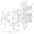
図1は、4WD車に用いられるパワーコントロールユニット(PCU)10と、2つの電動機70,72と1つの発電機71とを示す構成図で、ここではPCU10に車両用インバータユニット20が含まれている。電動機70は前輪走行駆動用であり、発電機71は回生発電用であり、電動機72は後輪走行駆動用である。 FIG. 1 is a configuration diagram showing a power control unit (PCU) 10 used in a 4WD vehicle, two
PCU10は、インバータ回路モジュール30とコンデンサモジュール40とを含む車両用インバータユニット20と、直流電源部60とから構成され、直流電源部60からの直流電力をコンデンサモジュール40に含まれる共通平滑コンデンサ42で平滑に維持しつつ、インバータ回路モジュール30で交流に変換し、2つの電動機70,72に供給する等の機能を有する車両搭載型の電源制御ユニットである。ここでインバータ回路モジュール30は、電動機70と発電機71とにそれぞれ対応する前輪走行駆動用インバータ回路31及び回生発電機用インバータ回路33とを含む主インバータ回路モジュール32と、電動機72に対応する後輪走行駆動用インバータ回路からなる副インバータ回路モジュール34とからなる。また、直流電源部60は、直流電源62と、リアクトル型昇圧回路64とを含む。 The
各インバータ回路モジュール32,34は、周知のインバータ回路を筐体ケースに収納し、それぞれ1つのモジュールとなしたものである。ここでインバータ回路とは、例えば車両の走行駆動時には、スイッチング素子を用いて直流信号を所定のタイミングでスイッチングし、電動機70,72及び発電機71のU、V,W相の3相交流信号に変換する機能を有する高速スイッチング回路である。主インバータ回路モジュール32に含まれる各インバータ回路31,33及び副インバータ回路モジュール34を構成するインバータ回路は、それぞれ、対応する電動機70,72及び発電機71のU,V,W相に接続される端子のほか、コンデンサモジュール40に接続される外部端子を備える。 Each of the
すなわち、各インバータ回路モジュール32,34において、それぞれのインバータ回路のP側母線36及びN側母線38はそれぞれ筐体ケースの表面に外部端子として引き出される。ここでP側母線36とは、共通平滑コンデンサ42を介して直流電源部60に接続されるとき、直流電源部60の高電位側に接続される電源線をいい、N側母線38とは、同様の接続関係のとき、直流電源部60の低電位側に接続される電源線をいう。例えば、主インバータ回路モジュール32の2本のP側母線36及び2本のN側母線38は、例えば極性の同じ2本がまとめられて、それぞれP側電極端子45とN側電極端子47としてその筐体の表面に引き出され、同様に副インバータ回路モジュール34のP側母線36及びN側母線38はそれぞれP側電極端子49とN側電極端子51としてその筐体の表面に引き出される。各外部端子の筐体上における配置関係の詳細については後述する。 That is, in each
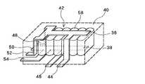
コンデンサモジュール40は、2つのインバータ回路モジュール32,34に対し、共通に用いられる平滑コンデンサ42を筐体ケースに収納し、1つのモジュールとなしたものである。コンデンサモジュール40は、直流電源部60と接続される1対の外部端子の他に、各インバータ回路モジュール32,34の各外部端子と結合によって接続される2対の外部端子を備える。 The
すなわち、共通平滑コンデンサ42のP側母線36及びN側母線38はそれぞれ3つに分岐する。ここでP側母線36、N側母線38とは、インバータ回路モジュール30で説明したように、直流電源部60に接続されるとき、直流電源部60の高電位側に接続される電源線がP側母線36で、直流電源部60の低電位側に接続される電源線がN側母線38である。その3組分岐のうち1組の末端は、それぞれ直流電源部60の高電位側及び低電位側と接続されるP電極端子52、N電極端子54としてコンデンサモジュール40の筐体から引き出される。 That is, the P-
共通平滑コンデンサ42のP側母線36の残る2つの分岐の末端はそれぞれ、主インバータ回路モジュール32のP側電極端子45に対応するP電極端子44と、副インバータ回路モジュール34のP側電極端子49に対応するP電極端子48として、コンデンサモジュール40の筐体から引き出される。同様に、共通平滑コンデンサ42のN側母線38の残る2つの分岐の末端はそれぞれ、主インバータ回路モジュール32のN側電極端子47に対応するN電極端子46と、副インバータ回路モジュール34のN側電極端子51に対応するN電極端子50として、コンデンサモジュール40の筐体から引き出される。各外部端子の筐体上における配置関係の詳細については後述する。 The remaining two branch ends of the P-
図2は、コンデンサモジュール40の内部構造を示す図である。コンデンサモジュール40の中には、共通平滑コンデンサ42が収納されている。共通平滑コンデンサ42は、整列配置された複数のフィルムコンデンサ素子58から構成され、各フィルムコンデンサ素子58の一方側の電極はそれぞれ共通の導体で接続され、これがP側母線36となる。同様に各フィルムコンデンサ素子58の他方側の電極はそれぞれ共通の導体で接続され、これがN側母線38となる。その意味で、フィルムコンデンサ素子58の一方側の電極をP電極、他方側の電極をN電極と呼ぶことができる。 FIG. 2 is a diagram showing the internal structure of the
図3は、フィルムコンデンサ素子58の製造方法の一例を通してその構造を説明する図である。図3(a)に示すように、フィルムコンデンサ素子を製造するには、まず、2枚の金属化フィルム55,56を巻き芯の周りにロール状に巻き取り、断面が略円形の半製品57を作る。金属化フィルムとは、例えばポリプロンフィルム等のプラスチックフィルムを誘電体として用い、その片面にコンデンサ電極となる金属層を蒸着技術等により形成したものである。各金属化フィルム55,56の端部からは引出電極部が設けられる。各金属化フィルム55,56の引出電極部は、互いに反対側の端部となるように設けられる。したがって、断面が円形の半製品57の軸方向における両端がそれぞれ引出電極部となる。次に図3(b)に示すように、断面が円形の半製品の巻き芯を抜き、矢印のように加圧して巻き芯の抜けた空洞を押しつぶして断面が長円形の扁平形のものとする。その後、その軸方向の両端にそれぞれ亜鉛溶射技術等により形成し、両端がそれぞれ電極となるフィルムコンデンサ素子58が完成する。このようにして製造されるフィルムコンデンサ素子58を必要な数だけ整列配置し、並列接続することで、必要な容量を有するコンデンサモジュール40を得ることができる。 FIG. 3 is a diagram illustrating the structure through an example of a method for manufacturing the
再び図2に戻り、コンデンサモジュール40のP側母線36、N側母線38は、上記のようにそれぞれ3つに分岐し、それぞれの末端は、コンデンサモジュール40の筐体から外側に引き出され、6つの外部端子となる。 Returning to FIG. 2 again, the P-
図2に示すように、P側母線36は複数のフィルムコンデンサ素子58の一方側電極部をそれぞれ接続して配置される上部電極板である。このP側母線36の上部電極板は、そのほぼ中央部で横方向に分岐し、コンデンサモジュール40の1つの側面に沿って下方に折れ曲がり、コンデンサモジュール40の底面の付近でさらに外部側に向けて折れ曲がってP電極端子44となる。また、このP側母線36の上部電極板は、その上部の端部で2つに分岐し、先ほどのP電極端子44が配置されるコンデンサモジュール40の側面とは異なる側面に沿ってそれぞれ下方に折れ曲がり、コンデンサモジュール40の底面の付近でさらにそれぞれ外部側に向けて折れ曲がって、P電極端子48,52となる。 As shown in FIG. 2, the P-
N側母線38は複数のフィルムコンデンサ素子58の他方側電極部をそれぞれ接続して配置される下部電極板である。このN側母線38の下部電極板は、そのほぼ中央部で、先ほどのP電極端子44と平行で、かつ互いに間隔をあけるように平行に横方向に分岐し、コンデンサモジュール40の底面の付近で外部側に出てN電極端子46となる。また、このN側母線38の下部電極板は、先ほどのP電極端子48,52が配置されるコンデンサモジュール40の側面のところで2つに分岐し、それぞれ外部側に出てN電極端子50,54となる。このときの分岐は、先ほどのP電極端子48,52と平行で、かつ互いに間隔をあけるように行われる。 The N-
このように、外部端子として、コンデンサモジュール40の1つの側面の底面側に1組のP電極端子44とN電極端子46が配置され、これと異なる側面の底面側には、P電極端子48とN電極端子50の組と、P電極端子52とN電極端子54の組の2組が配置される。なお、上部電極板、下部電極板の分岐や、その引出しの仕方はこれ以外のものであってもよい。また、この3組の外部端子は、それぞれ高さ方向の位置関係が相互に異なるものとすることができる。 As described above, a pair of
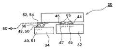
図4と図5は、それぞれ、車両用インバータユニット20の斜視図と側面図である。車両用インバータユニット20は、主インバータ回路モジュール32と副インバータ回路モジュール34の上部にコンデンサモジュール40を積み重ね、それぞれ対応する外部端子をボルト66で結合するものである。上記のように、主インバータ回路モジュール32は前輪走行駆動及び回生発電機用であり、副インバータ回路モジュール34は後輪走行駆動用であるので、後者は前者に比べやや小ぶりの外形を有する。 4 and 5 are a perspective view and a side view of the
ここで、主インバータ回路モジュール32は、その上面において図4で手前側に示す位置にP側電極端子45とN側電極端子47とがそれぞれナット穴を有する電極板として引き出されて埋め込まれている。また同様に、副インバータ回路モジュール34は、その上面において図4で左側に示す位置にP側電極端子49とN側電極端子51とがそれぞれナット穴を有する電極板として引き出されて埋め込まれている。また、コンデンサモジュール40はその底面側において、図4で手前側に示す位置にP電極端子44とN電極端子46とがそれぞれボルト66を通す穴を有する電極板として引き出される。また同様に、図4で左側に示す位置にP電極端子48とN電極端子50とがそれぞれボルトを通す穴を有する電極板として引き出される。さらに、図4で左側に示す位置にP電極端子52とN電極端子54とがそれぞれ引き出される。 Here, the main
これらにおいて、コンデンサモジュール40のP電極端子44の穴とN電極端子46の穴の相対配置関係は、主インバータ回路モジュール32のP側電極端子45のナット穴とN側電極端子47のナット穴の相対配置と同じにされる。すなわち、コンデンサモジュール40のP電極端子44の穴に主インバータ回路モジュール32のP側電極端子45のナット穴を合わせると同時に、コンデンサモジュール40のN電極端子46の穴に主インバータ回路モジュール32のN側電極端子47のナット穴を合わせることができる。 In these, the relative arrangement relationship between the hole of the
また、同様にコンデンサモジュール40のP電極端子48の穴とN電極端子50の穴の相対配置関係は、副インバータ回路モジュール34のP側電極端子49のナット穴とN側電極端子51のナット穴の相対配置と同じにされる。さらに、この配置関係は、上記コンデンサモジュール40と主インバータ回路モジュール32との間の配置関係と関係付けられる。すなわち、上記のようにコンデンサモジュール40のP電極端子44とN電極端子46とを主インバータ回路モジュール32のP側電極端子45とN側電極端子47にそれぞれ合わせた状態で、コンデンサモジュール40のP電極端子48の穴に副インバータ回路モジュール34のP側電極端子49のナット穴を合わせると同時に、コンデンサモジュール40のN電極端子50の穴に副インバータ回路モジュール34のN側電極端子51のナット穴を合わせることができる。 Similarly, the relative arrangement relationship between the hole of the
このようにして、コンデンサモジュール40の各外部端子は、それぞれ主インバータ回路モジュール32において対応する各外部端子と、副インバータ回路モジュール34において対応する各外部端子と、それぞれ平面配置関係及び高さ配置関係を含めて、ボルト66によって結合できるように配置される。なお、コンデンサモジュール40から引き出された残りのP電極端子52とN電極端子54は、それぞれバスバー等の適当な接続線部材を用いて直流電源部60に接続される。 In this way, the external terminals of the
したがって、主インバータ回路モジュール32と副インバータ回路モジュール34の上部にコンデンサモジュール40を積み重ね、それぞれ対応する外部端子をボルト66で結合することで、インバータ回路とコンデンサとの間のインピーダンスを低くするとともに、全体として小型化を図ることができ、車両搭載において自由度が増す。また、FF車のように、副インバータ回路モジュール34が必要でない車両を製造するときには、コンデンサモジュール40と副インバータ回路モジュール34とを結合するボルト66を外すことで、副インバータ回路モジュール34を含まない車両用インバータモジュールを容易に得ることができる。 Accordingly, the
10 PCU、20 車両用インバータユニット、30 インバータ回路モジュール、31,33 インバータ回路、32 主インバータ回路モジュール、34 副インバータ回路モジュール、36 P側母線、38 N側母線、40 コンデンサモジュール、42 共通平滑コンデンサ、44,48,52 P電極端子、45,49 P側電極端子、46,50,54 N電極端子、47,51 N側電極端子、55,56 金属化フィルム、57 半製品、58 フィルムコンデンサ素子、60 直流電源部、62 直流電源、64 昇圧回路、66 ボルト、70,72 電動機、71 発電機。 10 PCU, 20 inverter unit for vehicle, 30 inverter circuit module, 31, 33 inverter circuit, 32 main inverter circuit module, 34 sub inverter circuit module, 36 P side bus, 38 N side bus, 40 capacitor module, 42
Claims (4)
Translated fromJapanese複数対のP電極端子及びN電極端子を外部端子として有する平滑コンデンサであって、各P電極端子及び各N電極端子のそれぞれは平滑コンデンサの内部素子のP電極又はN電極からそれぞれ複数に分岐し、複数のインバータ回路モジュールの各P側電極端子及び各N側電極端子とそれぞれ着脱可能に結合される共通平滑コンデンサと、
を備えることを特徴とする車両用インバータユニット。A plurality of inverter circuit modules having P-side electrode terminals and N-side electrode terminals as external terminals;
A smoothing capacitor having a plurality of pairs of P electrode terminals and N electrode terminals as external terminals, wherein each of the P electrode terminals and each of the N electrode terminals branches into a plurality from the P electrode or N electrode of the internal element of the smoothing capacitor. A common smoothing capacitor detachably coupled to each P-side electrode terminal and each N-side electrode terminal of the plurality of inverter circuit modules;
A vehicle inverter unit comprising:
共通平滑コンデンサの各外部端子は、各インバータ回路モジュールの外部端子の高さに対応する高さ位置にそれぞれ配置されることを特徴とする車両用インバータユニット。In the vehicle inverter unit according to claim 1,
Each of the external terminals of the common smoothing capacitor is disposed at a height position corresponding to the height of the external terminal of each inverter circuit module.
共通平滑コンデンサは、略直方体の外形を有し、その各側面に各インバータ回路モジュールの外部端子に対応する1対ずつの外部端子が配置されることを特徴とする車両用インバータユニット。In the vehicle inverter unit according to claim 1,
The common smoothing capacitor has a substantially rectangular parallelepiped outer shape, and a pair of external terminals corresponding to the external terminals of each inverter circuit module are arranged on each side surface of the common smoothing capacitor.
複数のインバータ回路モジュールは、
車両の前輪駆動の走行駆動及び発電用に用いられる主インバータ回路モジュールと、
車両の後輪駆動の走行駆動用に用いられる副インバータ回路モジュールと、
を含むことを特徴とする車両用インバータユニット。
In the vehicle inverter unit according to claim 1,
Multiple inverter circuit modules
A main inverter circuit module used for driving and power generation of the front wheel drive of the vehicle;
A sub-inverter circuit module used for driving driving of the rear wheel drive of the vehicle;
The inverter unit for vehicles characterized by including.
Priority Applications (3)
| Application Number | Priority Date | Filing Date | Title |
|---|---|---|---|
| JP2005078987AJP2006262665A (en) | 2005-03-18 | 2005-03-18 | Inverter unit for vehicle |
| US11/366,659US20060208660A1 (en) | 2005-03-18 | 2006-03-03 | Inverter unit for vehicle |
| CNA2006100585542ACN1835357A (en) | 2005-03-18 | 2006-03-16 | Inverter unit for vehicle |
Applications Claiming Priority (1)
| Application Number | Priority Date | Filing Date | Title |
|---|---|---|---|
| JP2005078987AJP2006262665A (en) | 2005-03-18 | 2005-03-18 | Inverter unit for vehicle |
Publications (1)
| Publication Number | Publication Date |
|---|---|
| JP2006262665Atrue JP2006262665A (en) | 2006-09-28 |
Family
ID=37003003
Family Applications (1)
| Application Number | Title | Priority Date | Filing Date |
|---|---|---|---|
| JP2005078987AWithdrawnJP2006262665A (en) | 2005-03-18 | 2005-03-18 | Inverter unit for vehicle |
Country Status (3)
| Country | Link |
|---|---|
| US (1) | US20060208660A1 (en) |
| JP (1) | JP2006262665A (en) |
| CN (1) | CN1835357A (en) |
Cited By (12)
| Publication number | Priority date | Publication date | Assignee | Title |
|---|---|---|---|---|
| JP2008206312A (en)* | 2007-02-20 | 2008-09-04 | Canon Inc | Power supply device and image forming apparatus having the power supply device |
| JP2008295238A (en)* | 2007-05-25 | 2008-12-04 | Mitsubishi Electric Corp | Power converter |
| KR100891430B1 (en) | 2007-08-07 | 2009-04-06 | 엘에스산전 주식회사 | Hybrid car inverter |
| JP2010115089A (en)* | 2008-11-10 | 2010-05-20 | Mitsubishi Electric Corp | Power conversion apparatus |
| JP2011109898A (en)* | 2009-10-31 | 2011-06-02 | Semikron Elektronik Gmbh & Co Kg | Converter with module structure |
| JP2013027182A (en)* | 2011-07-22 | 2013-02-04 | Hitachi Industrial Equipment Systems Co Ltd | Electric power conversion device |
| JP2013059191A (en)* | 2011-09-08 | 2013-03-28 | Denso Corp | Electric power conversion apparatus |
| JP2015154586A (en)* | 2014-02-14 | 2015-08-24 | 株式会社 Acr | Connection plate-mounting substrate for capacitor |
| JP2017184613A (en)* | 2017-06-07 | 2017-10-05 | 三菱電機株式会社 | Power converter |
| US10148190B2 (en) | 2015-04-20 | 2018-12-04 | Mitsubishi Electric Corporation | Power conversion device |
| WO2022044228A1 (en)* | 2020-08-27 | 2022-03-03 | 日産自動車株式会社 | Power conversion device |
| WO2022168569A1 (en) | 2021-02-05 | 2022-08-11 | 株式会社明電舎 | Electrical device |
Families Citing this family (73)
| Publication number | Priority date | Publication date | Assignee | Title |
|---|---|---|---|---|
| JP4859443B2 (en) | 2005-11-17 | 2012-01-25 | 日立オートモティブシステムズ株式会社 | Power converter |
| US10693415B2 (en) | 2007-12-05 | 2020-06-23 | Solaredge Technologies Ltd. | Testing of a photovoltaic panel |
| US11881814B2 (en) | 2005-12-05 | 2024-01-23 | Solaredge Technologies Ltd. | Testing of a photovoltaic panel |
| US8319483B2 (en) | 2007-08-06 | 2012-11-27 | Solaredge Technologies Ltd. | Digital average input current control in power converter |
| US11735910B2 (en) | 2006-12-06 | 2023-08-22 | Solaredge Technologies Ltd. | Distributed power system using direct current power sources |
| US11855231B2 (en) | 2006-12-06 | 2023-12-26 | Solaredge Technologies Ltd. | Distributed power harvesting systems using DC power sources |
| US11687112B2 (en) | 2006-12-06 | 2023-06-27 | Solaredge Technologies Ltd. | Distributed power harvesting systems using DC power sources |
| US8013472B2 (en) | 2006-12-06 | 2011-09-06 | Solaredge, Ltd. | Method for distributed power harvesting using DC power sources |
| US11296650B2 (en) | 2006-12-06 | 2022-04-05 | Solaredge Technologies Ltd. | System and method for protection during inverter shutdown in distributed power installations |
| US8384243B2 (en) | 2007-12-04 | 2013-02-26 | Solaredge Technologies Ltd. | Distributed power harvesting systems using DC power sources |
| US9130401B2 (en) | 2006-12-06 | 2015-09-08 | Solaredge Technologies Ltd. | Distributed power harvesting systems using DC power sources |
| US20080144294A1 (en)* | 2006-12-06 | 2008-06-19 | Meir Adest | Removal component cartridge for increasing reliability in power harvesting systems |
| US9088178B2 (en) | 2006-12-06 | 2015-07-21 | Solaredge Technologies Ltd | Distributed power harvesting systems using DC power sources |
| US12316274B2 (en) | 2006-12-06 | 2025-05-27 | Solaredge Technologies Ltd. | Pairing of components in a direct current distributed power generation system |
| US8473250B2 (en) | 2006-12-06 | 2013-06-25 | Solaredge, Ltd. | Monitoring of distributed power harvesting systems using DC power sources |
| US8963369B2 (en) | 2007-12-04 | 2015-02-24 | Solaredge Technologies Ltd. | Distributed power harvesting systems using DC power sources |
| US8816535B2 (en) | 2007-10-10 | 2014-08-26 | Solaredge Technologies, Ltd. | System and method for protection during inverter shutdown in distributed power installations |
| US11569659B2 (en) | 2006-12-06 | 2023-01-31 | Solaredge Technologies Ltd. | Distributed power harvesting systems using DC power sources |
| US11309832B2 (en) | 2006-12-06 | 2022-04-19 | Solaredge Technologies Ltd. | Distributed power harvesting systems using DC power sources |
| US8618692B2 (en) | 2007-12-04 | 2013-12-31 | Solaredge Technologies Ltd. | Distributed power system using direct current power sources |
| US8319471B2 (en) | 2006-12-06 | 2012-11-27 | Solaredge, Ltd. | Battery power delivery module |
| US9112379B2 (en) | 2006-12-06 | 2015-08-18 | Solaredge Technologies Ltd. | Pairing of components in a direct current distributed power generation system |
| US8947194B2 (en) | 2009-05-26 | 2015-02-03 | Solaredge Technologies Ltd. | Theft detection and prevention in a power generation system |
| US11888387B2 (en) | 2006-12-06 | 2024-01-30 | Solaredge Technologies Ltd. | Safety mechanisms, wake up and shutdown methods in distributed power installations |
| WO2009072076A2 (en) | 2007-12-05 | 2009-06-11 | Solaredge Technologies Ltd. | Current sensing on a mosfet |
| US9291696B2 (en) | 2007-12-05 | 2016-03-22 | Solaredge Technologies Ltd. | Photovoltaic system power tracking method |
| WO2009073867A1 (en) | 2007-12-05 | 2009-06-11 | Solaredge, Ltd. | Parallel connected inverters |
| EP2225778B1 (en) | 2007-12-05 | 2019-06-26 | Solaredge Technologies Ltd. | Testing of a photovoltaic panel |
| US11264947B2 (en) | 2007-12-05 | 2022-03-01 | Solaredge Technologies Ltd. | Testing of a photovoltaic panel |
| CN105244905B (en) | 2007-12-05 | 2019-05-21 | 太阳能安吉有限公司 | Release mechanism in distributed power device is waken up and method for closing |
| JP4580997B2 (en) | 2008-03-11 | 2010-11-17 | 日立オートモティブシステムズ株式会社 | Power converter |
| US8111052B2 (en) | 2008-03-24 | 2012-02-07 | Solaredge Technologies Ltd. | Zero voltage switching |
| EP2294669B8 (en) | 2008-05-05 | 2016-12-07 | Solaredge Technologies Ltd. | Direct current power combiner |
| US8630098B2 (en) | 2008-06-12 | 2014-01-14 | Solaredge Technologies Ltd. | Switching circuit layout with heatsink |
| JP4644275B2 (en) | 2008-07-29 | 2011-03-02 | 日立オートモティブシステムズ株式会社 | Power converter and electric vehicle |
| EP2602831B1 (en) | 2009-05-22 | 2014-07-16 | Solaredge Technologies Ltd. | Electrically isolated heat dissipating junction box |
| US8303349B2 (en) | 2009-05-22 | 2012-11-06 | Solaredge Technologies Ltd. | Dual compressive connector |
| US8690110B2 (en) | 2009-05-25 | 2014-04-08 | Solaredge Technologies Ltd. | Bracket for connection of a junction box to photovoltaic panels |
| US8130501B2 (en)* | 2009-06-30 | 2012-03-06 | Teco-Westinghouse Motor Company | Pluggable power cell for an inverter |
| AU2009349618B2 (en)* | 2009-07-06 | 2013-10-03 | Mitsubishi Electric Corporation | Power conversion device |
| US12418177B2 (en) | 2009-10-24 | 2025-09-16 | Solaredge Technologies Ltd. | Distributed power system using direct current power sources |
| US8710699B2 (en) | 2009-12-01 | 2014-04-29 | Solaredge Technologies Ltd. | Dual use photovoltaic system |
| DE102010004713A1 (en)* | 2010-01-11 | 2011-07-14 | Dr. Ing. h.c. F. Porsche Aktiengesellschaft, 70435 | Hybrid drive of a hybrid vehicle |
| US8766696B2 (en) | 2010-01-27 | 2014-07-01 | Solaredge Technologies Ltd. | Fast voltage level shifter circuit |
| KR20110135233A (en)* | 2010-06-10 | 2011-12-16 | 현대자동차주식회사 | Capacitors for inverters of automobiles |
| GB2485527B (en) | 2010-11-09 | 2012-12-19 | Solaredge Technologies Ltd | Arc detection and prevention in a power generation system |
| US10673222B2 (en) | 2010-11-09 | 2020-06-02 | Solaredge Technologies Ltd. | Arc detection and prevention in a power generation system |
| US10230310B2 (en) | 2016-04-05 | 2019-03-12 | Solaredge Technologies Ltd | Safety switch for photovoltaic systems |
| US10673229B2 (en) | 2010-11-09 | 2020-06-02 | Solaredge Technologies Ltd. | Arc detection and prevention in a power generation system |
| GB2486408A (en) | 2010-12-09 | 2012-06-20 | Solaredge Technologies Ltd | Disconnection of a string carrying direct current |
| GB2483317B (en) | 2011-01-12 | 2012-08-22 | Solaredge Technologies Ltd | Serially connected inverters |
| JP5363598B2 (en)* | 2011-04-07 | 2013-12-11 | ファナック株式会社 | Motor drive controller that can be connected to a DC / AC converter |
| US8570005B2 (en) | 2011-09-12 | 2013-10-29 | Solaredge Technologies Ltd. | Direct current link circuit |
| GB2498365A (en) | 2012-01-11 | 2013-07-17 | Solaredge Technologies Ltd | Photovoltaic module |
| GB2498791A (en) | 2012-01-30 | 2013-07-31 | Solaredge Technologies Ltd | Photovoltaic panel circuitry |
| GB2498790A (en) | 2012-01-30 | 2013-07-31 | Solaredge Technologies Ltd | Maximising power in a photovoltaic distributed power system |
| US9853565B2 (en) | 2012-01-30 | 2017-12-26 | Solaredge Technologies Ltd. | Maximized power in a photovoltaic distributed power system |
| GB2499991A (en) | 2012-03-05 | 2013-09-11 | Solaredge Technologies Ltd | DC link circuit for photovoltaic array |
| EP3499695B1 (en) | 2012-05-25 | 2024-09-18 | Solaredge Technologies Ltd. | Circuit for interconnected direct current power sources |
| US10115841B2 (en) | 2012-06-04 | 2018-10-30 | Solaredge Technologies Ltd. | Integrated photovoltaic panel circuitry |
| US9548619B2 (en) | 2013-03-14 | 2017-01-17 | Solaredge Technologies Ltd. | Method and apparatus for storing and depleting energy |
| US9941813B2 (en) | 2013-03-14 | 2018-04-10 | Solaredge Technologies Ltd. | High frequency multi-level inverter |
| EP3506370B1 (en) | 2013-03-15 | 2023-12-20 | Solaredge Technologies Ltd. | Bypass mechanism |
| US9318974B2 (en) | 2014-03-26 | 2016-04-19 | Solaredge Technologies Ltd. | Multi-level inverter with flying capacitor topology |
| US10490357B2 (en)* | 2015-09-28 | 2019-11-26 | Kyocera Corporation | Film capacitor, combination type capacitor, inverter, and electric vehicle |
| CN107153212B (en) | 2016-03-03 | 2023-07-28 | 太阳能安吉科技有限公司 | Method for mapping a power generation facility |
| US10599113B2 (en) | 2016-03-03 | 2020-03-24 | Solaredge Technologies Ltd. | Apparatus and method for determining an order of power devices in power generation systems |
| US11081608B2 (en) | 2016-03-03 | 2021-08-03 | Solaredge Technologies Ltd. | Apparatus and method for determining an order of power devices in power generation systems |
| US12057807B2 (en) | 2016-04-05 | 2024-08-06 | Solaredge Technologies Ltd. | Chain of power devices |
| US11177663B2 (en) | 2016-04-05 | 2021-11-16 | Solaredge Technologies Ltd. | Chain of power devices |
| US11018623B2 (en) | 2016-04-05 | 2021-05-25 | Solaredge Technologies Ltd. | Safety switch for photovoltaic systems |
| DE102017212853A1 (en)* | 2017-07-26 | 2019-01-31 | Volkswagen Aktiengesellschaft | Highly integrated power converter system and motor vehicle |
| JP2019118244A (en)* | 2017-12-27 | 2019-07-18 | 日本電産トーソク株式会社 | motor |
- 2005
- 2005-03-18JPJP2005078987Apatent/JP2006262665A/ennot_activeWithdrawn
- 2006
- 2006-03-03USUS11/366,659patent/US20060208660A1/ennot_activeAbandoned
- 2006-03-16CNCNA2006100585542Apatent/CN1835357A/enactivePending
Cited By (14)
| Publication number | Priority date | Publication date | Assignee | Title |
|---|---|---|---|---|
| JP2008206312A (en)* | 2007-02-20 | 2008-09-04 | Canon Inc | Power supply device and image forming apparatus having the power supply device |
| JP2008295238A (en)* | 2007-05-25 | 2008-12-04 | Mitsubishi Electric Corp | Power converter |
| KR100891430B1 (en) | 2007-08-07 | 2009-04-06 | 엘에스산전 주식회사 | Hybrid car inverter |
| JP2010115089A (en)* | 2008-11-10 | 2010-05-20 | Mitsubishi Electric Corp | Power conversion apparatus |
| JP2011109898A (en)* | 2009-10-31 | 2011-06-02 | Semikron Elektronik Gmbh & Co Kg | Converter with module structure |
| JP2013027182A (en)* | 2011-07-22 | 2013-02-04 | Hitachi Industrial Equipment Systems Co Ltd | Electric power conversion device |
| JP2013059191A (en)* | 2011-09-08 | 2013-03-28 | Denso Corp | Electric power conversion apparatus |
| JP2015154586A (en)* | 2014-02-14 | 2015-08-24 | 株式会社 Acr | Connection plate-mounting substrate for capacitor |
| US10148190B2 (en) | 2015-04-20 | 2018-12-04 | Mitsubishi Electric Corporation | Power conversion device |
| JP2017184613A (en)* | 2017-06-07 | 2017-10-05 | 三菱電機株式会社 | Power converter |
| WO2022044228A1 (en)* | 2020-08-27 | 2022-03-03 | 日産自動車株式会社 | Power conversion device |
| JP7571790B2 (en) | 2020-08-27 | 2024-10-23 | 日産自動車株式会社 | Power Conversion Equipment |
| WO2022168569A1 (en) | 2021-02-05 | 2022-08-11 | 株式会社明電舎 | Electrical device |
| US12069797B2 (en) | 2021-02-05 | 2024-08-20 | Meidensha Corporation | Electrical device |
Also Published As
| Publication number | Publication date |
|---|---|
| CN1835357A (en) | 2006-09-20 |
| US20060208660A1 (en) | 2006-09-21 |
Similar Documents
| Publication | Publication Date | Title |
|---|---|---|
| JP2006262665A (en) | Inverter unit for vehicle | |
| JP6805932B2 (en) | vehicle | |
| CN102025319B (en) | Low Inductance Power Electronic Components | |
| CN102064672B (en) | Power electronics assembly with multi-sided inductor cooling | |
| US20160229293A1 (en) | Electrically driven vehicle | |
| CN101873076A (en) | power conversion device | |
| JP6646739B2 (en) | Power converter | |
| CN101901797B (en) | Power electronics power module with imbedded gate circuitry | |
| EP3496519A1 (en) | Electrical device and manufacturing method of the same | |
| JP7594366B2 (en) | Vehicle battery unit | |
| CN101997403A (en) | Electromagnetic interference filter for automotive electrical systems | |
| CN111137141A (en) | Motorized vehicle with low-profile bus for high-current interface | |
| CN220421607U (en) | Controller, electric assembly, drive system and vehicle | |
| CN109600052B (en) | Vehicle-mounted structure of power converter | |
| US12280685B2 (en) | Power distribution device | |
| JP2016116340A (en) | Power conversion unit | |
| CN114825909A (en) | Power distribution structure of battery package, battery package and vehicle | |
| US7924134B2 (en) | Inductor packaging for power converters | |
| JP2005117728A (en) | Power module connection structure in the inverter unit | |
| JP2016149911A (en) | Power converter | |
| US12257909B2 (en) | Electromechanical integration unit | |
| JP6520190B2 (en) | Wiring structure of vehicle harness | |
| CN114423632B (en) | Drive device for an electrically drivable motor vehicle and motor vehicle | |
| CN212011905U (en) | High-voltage electric box | |
| CN101420170B (en) | Compact terminal assembly for power converter |
Legal Events
| Date | Code | Title | Description |
|---|---|---|---|
| A621 | Written request for application examination | Free format text:JAPANESE INTERMEDIATE CODE: A621 Effective date:20070125 | |
| A761 | Written withdrawal of application | Free format text:JAPANESE INTERMEDIATE CODE: A761 Effective date:20081027 |