JP2006262421A - Semiconductor integrated circuit and noise reduction method thereof - Google Patents
Semiconductor integrated circuit and noise reduction method thereofDownload PDFInfo
- Publication number
- JP2006262421A JP2006262421AJP2005080702AJP2005080702AJP2006262421AJP 2006262421 AJP2006262421 AJP 2006262421AJP 2005080702 AJP2005080702 AJP 2005080702AJP 2005080702 AJP2005080702 AJP 2005080702AJP 2006262421 AJP2006262421 AJP 2006262421A
- Authority
- JP
- Japan
- Prior art keywords
- input
- circuit
- input buffer
- circuits
- threshold
- Prior art date
- Legal status (The legal status is an assumption and is not a legal conclusion. Google has not performed a legal analysis and makes no representation as to the accuracy of the status listed.)
- Withdrawn
Links
Images


Classifications
- H—ELECTRICITY
- H03—ELECTRONIC CIRCUITRY
- H03K—PULSE TECHNIQUE
- H03K19/00—Logic circuits, i.e. having at least two inputs acting on one output; Inverting circuits
- H03K19/0175—Coupling arrangements; Interface arrangements
- H—ELECTRICITY
- H03—ELECTRONIC CIRCUITRY
- H03K—PULSE TECHNIQUE
- H03K5/00—Manipulating of pulses not covered by one of the other main groups of this subclass
- H03K5/01—Shaping pulses
- H03K5/08—Shaping pulses by limiting; by thresholding; by slicing, i.e. combined limiting and thresholding
- H—ELECTRICITY
- H03—ELECTRONIC CIRCUITRY
- H03K—PULSE TECHNIQUE
- H03K17/00—Electronic switching or gating, i.e. not by contact-making and –breaking
- H03K17/30—Modifications for providing a predetermined threshold before switching
- H03K17/302—Modifications for providing a predetermined threshold before switching in field-effect transistor switches
- H—ELECTRICITY
- H03—ELECTRONIC CIRCUITRY
- H03K—PULSE TECHNIQUE
- H03K17/00—Electronic switching or gating, i.e. not by contact-making and –breaking
- H03K17/51—Electronic switching or gating, i.e. not by contact-making and –breaking characterised by the components used
- H03K17/56—Electronic switching or gating, i.e. not by contact-making and –breaking characterised by the components used by the use, as active elements, of semiconductor devices
- H03K17/687—Electronic switching or gating, i.e. not by contact-making and –breaking characterised by the components used by the use, as active elements, of semiconductor devices the devices being field-effect transistors
- H03K17/693—Switching arrangements with several input- or output-terminals, e.g. multiplexers, distributors
- H—ELECTRICITY
- H03—ELECTRONIC CIRCUITRY
- H03K—PULSE TECHNIQUE
- H03K19/00—Logic circuits, i.e. having at least two inputs acting on one output; Inverting circuits
- H03K19/003—Modifications for increasing the reliability for protection
- H03K19/00346—Modifications for eliminating interference or parasitic voltages or currents
- H—ELECTRICITY
- H03—ELECTRONIC CIRCUITRY
- H03K—PULSE TECHNIQUE
- H03K19/00—Logic circuits, i.e. having at least two inputs acting on one output; Inverting circuits
- H03K19/01—Modifications for accelerating switching
Landscapes
- Physics & Mathematics (AREA)
- Engineering & Computer Science (AREA)
- Computer Hardware Design (AREA)
- Computing Systems (AREA)
- General Engineering & Computer Science (AREA)
- Mathematical Physics (AREA)
- Nonlinear Science (AREA)
- Logic Circuits (AREA)
Abstract
Translated fromJapaneseDescription
Translated fromJapanese 本発明は、例えば、CMOS(Complementary Metal Oxide Semiconductor )回路の素子間に流れる貫通電流等、入力により電気的な状態変化を生じる複数の素子又は回路を含む半導体集積回路に関し、特に、共通の入力により同時に電気的な状態変化を生じる複数の素子又はCMOS回路等の回路を備えた半導体集積回路及びそのノイズ低減方法に関する。
The present invention relates to a semiconductor integrated circuit including a plurality of elements or circuits that cause an electrical state change by input, such as a through current flowing between elements of a CMOS (Complementary Metal Oxide Semiconductor) circuit, and in particular, by a common input. The present invention relates to a semiconductor integrated circuit including a plurality of elements or a circuit such as a CMOS circuit that causes an electrical state change at the same time and a noise reduction method thereof.
半導体集積回路として例えば、LSI(Large Scale Integration )では多ピン化及び高密度化が図られているが、斯かる半導体集積回路では、多数の入出力回路が実装されている。これら入出力回路が入力信号により同時にスイッチングした場合、そのスイッチングによるノイズの影響を無視することができない。このスイッチングノイズの発生は、入力切換えに伴い、スイッチング電流による電源変動やGND電位の変動が主な要因である。 As a semiconductor integrated circuit, for example, LSI (Large Scale Integration) attempts to increase the number of pins and increase the density. However, in such a semiconductor integrated circuit, a large number of input / output circuits are mounted. When these input / output circuits are simultaneously switched by an input signal, the influence of noise due to the switching cannot be ignored. The generation of this switching noise is mainly caused by power supply fluctuations due to switching currents and fluctuations in the GND potential accompanying input switching.
素子や回路の同時スイッチングによるノイズの影響は、入力信号の立上り又は立下り、入力信号振幅、同時に切り換わる信号の数に依存している。特に、データバス等、複数ビットの信号伝送路では、同時に多数の信号が同一タイミングで切り換わる。同時導通の数が多くなればなる程、スイッチングノイズの発生がより顕著となる。例えば、CMOS回路の場合では、信号の切換え時に電流が流れるが、反射波形により中間レベルに一定レベルの区間(段)を持つ場合には、その中間レベル位置(図6のΔt)で貫通電流が流れることになり、これもノイズ源となる。 The influence of noise due to simultaneous switching of elements and circuits depends on the rising or falling of the input signal, the input signal amplitude, and the number of signals that are simultaneously switched. In particular, in a multi-bit signal transmission line such as a data bus, a large number of signals are switched at the same timing at the same time. As the number of simultaneous conductions increases, the generation of switching noise becomes more remarkable. For example, in the case of a CMOS circuit, a current flows at the time of signal switching. However, when there is a section (stage) at a certain level at an intermediate level due to a reflected waveform, a through current flows at the intermediate level position (Δt in FIG. 6). Will flow, and this will also be a source of noise.
斯かる半導体集積回路に関し、CMOS回路の論理しきい値によってスイッチング速度を異ならせたものとして例えば、特許文献1がある。
ところで、半導体集積回路に共通の入力を同時に受けて導通する多数の素子や回路を含む場合には、電源から半導体集積回路を通して接地側に流れる電流が素子や回路の導通数に応じて大きくなる。ノイズは、この電流値の大きさや変化に依存しており、斯かるノイズを低減するには、その電流値を抑制すればよい。しかしながら、多ピン化及び高密度化により高機能化、多機能化している半導体集積回路では、単純に電流を抑制すれば、その回路機能を損なうおそれがある。By the way, when a semiconductor integrated circuit includes a large number of elements and circuits that receive a common input at the same time and conduct, the current flowing from the power source to the ground side through the semiconductor integrated circuit increases in accordance with the number of conduction of the elements and circuits. Noise depends on the magnitude and change of the current value, and in order to reduce such noise, the current value may be suppressed. However, in a semiconductor integrated circuit that is highly functionalized and multifunctionalized by increasing the number of pins and increasing the density, if the current is simply suppressed, the circuit function may be impaired.
特許文献1にはCMOS回路の論理しきい値の値によってスイッチング速度を異ならせることを開示しているが、電流に依存するノイズ発生や、そのノイズの抑制についての課題やその解決手段についての開示や示唆はない。
そこで、本発明は、共通の入力を受けて状態変化を生ずる素子や回路を備える半導体集積回路に関し、入力による状態変化の生起タイミングを変移させることを目的とする。 SUMMARY OF THE INVENTION The present invention relates to a semiconductor integrated circuit including elements and circuits that generate a state change upon receiving a common input, and an object thereof is to change the occurrence timing of the state change caused by the input.
また、本発明は、共通の入力を受けて状態変化を生ずる素子や回路を備える半導体集積回路に関し、入力による状態変化に起因するノイズを低減させることを目的とする。
Another object of the present invention relates to a semiconductor integrated circuit including elements and circuits that generate a state change upon receiving a common input, and an object thereof is to reduce noise caused by the state change caused by the input.
上記目的を達成するため、本発明の半導体集積回路は、しきい値を異ならせた複数の素子又は回路を含み、これら素子又は回路に共通の入力が同時に加えられた場合に、前記しきい値に応じて異なる時期に状態変化を生じる構成としている。 In order to achieve the above object, a semiconductor integrated circuit according to the present invention includes a plurality of elements or circuits having different threshold values, and when a common input is simultaneously applied to these elements or circuits, the threshold value is increased. Depending on the situation, the state changes at different times.
斯かる構成とすれば、複数の素子又は回路は、入力により状態変化を生じ、その状態変化に応じて電流が流れる。これら複数の素子又は回路に異なるしきい値を設定すると、共通の入力を同時に受けた場合に、設定されているしきい値により、異なる時期に状態変化が生じ、電流の流れる時期も異なってくるので、そのピーク値はタイミングの相違により重畳されることがない。この結果、半導体集積回路に電源から流れ込む電流が大幅に低減され、その変化も抑制される。これにより、ノイズの発生が抑制され、また、ノイズが発生するにしても、その振幅が大幅に低減されることになる。 With such a configuration, a plurality of elements or circuits cause a state change by input, and a current flows in accordance with the state change. When different threshold values are set for these multiple elements or circuits, when a common input is received simultaneously, the state changes at different times and the current flows at different times depending on the set threshold values. Therefore, the peak value is not superimposed due to the timing difference. As a result, the current flowing from the power source into the semiconductor integrated circuit is greatly reduced, and the change is also suppressed. Thereby, generation | occurrence | production of noise is suppressed, and even if noise generate | occur | produces, the amplitude will be reduced significantly.
上記目的を達成するため、上記半導体集積回路において、前記素子は、トランジスタである構成としてもよい。 In order to achieve the above object, in the semiconductor integrated circuit, the element may be a transistor.
上記目的を達成するため、上記半導体集積回路において、前記回路は、CMOS回路である構成としてもよい。 In order to achieve the above object, in the semiconductor integrated circuit, the circuit may be a CMOS circuit.
上記目的を達成するため、上記半導体集積回路において、前記しきい値は、前記素子又は前記回路が持つ定数により設定した構成としてもよい。 In order to achieve the above object, in the semiconductor integrated circuit, the threshold value may be set by a constant of the element or the circuit.
上記目的を達成するため、本発明の半導体集積回路のノイズ低減方法は、複数の素子又は回路を含む半導体集積回路のノイズ低減方法であって、前記素子又は回路に異なるしきい値を設定し、同時に共通の入力を受けた場合に、前記しきい値に応じて異なる時期に状態変化を生じさせる構成である。 In order to achieve the above object, a noise reduction method for a semiconductor integrated circuit according to the present invention is a noise reduction method for a semiconductor integrated circuit including a plurality of elements or circuits, and sets different thresholds for the elements or circuits. When a common input is received at the same time, the state changes at different times according to the threshold value.
斯かる構成とすれば、既述の通り、しきい値を異ならせたことにより、同時に共通の入力を受けても、異なるしきい値に応じて異なる時期に状態変化を生じることになり、その状態変化に伴う電流値やその変化によるノイズ発生の抑制、ノイズ振幅を低減することができる。
With such a configuration, as described above, by changing the threshold value, even if a common input is received at the same time, a state change occurs at different times according to different threshold values. It is possible to suppress the generation of noise due to the current value accompanying the state change, the change, and the noise amplitude.
以上の構成によれば、次のような効果が得られる。 According to the above configuration, the following effects can be obtained.
(1) 複数の素子又は回路を含む半導体集積回路について、異なるしきい値を設定した複数の素子又は回路を含むので、共通の入力を同時に受けてもしきい値に応じた時期に状態変化を生ずるので、その状態変化に伴う電流のピーク値の重畳を防止でき、電流値及びその変化を大幅に低減できる。 (1) A semiconductor integrated circuit including a plurality of elements or circuits includes a plurality of elements or circuits set with different threshold values, so that even if a common input is received simultaneously, a state change occurs at a time corresponding to the threshold values. Therefore, it is possible to prevent the peak value of the current accompanying the state change from being superimposed, and to greatly reduce the current value and the change thereof.
(2) 電流値やその変化の低減により、ノイズ発生の抑制又はノイズ振幅の低減を図ることができ、複数の素子又は回路を含む半導体集積回路の誤動作等を防止でき、信頼性を向上させることができる。
(2) By reducing the current value and its change, noise generation can be suppressed or noise amplitude can be reduced, malfunction of a semiconductor integrated circuit including a plurality of elements or circuits can be prevented, and reliability can be improved. Can do.
第1の実施の形態 First embodiment
本発明の第1の実施の形態について、図1を参照して説明する。図1は、第1の実施の形態に係る半導体集積回路を示す回路図である。 A first embodiment of the present invention will be described with reference to FIG. FIG. 1 is a circuit diagram showing a semiconductor integrated circuit according to the first embodiment.
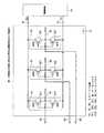
この半導体集積回路として例えば、LSI2には複数の入力バッファ回路として例えば、3組の入力バッファ回路41、42、43が設置されている。各入力バッファ回路41、42、43には異なるしきい値としてレベルの異なるしきい値電圧Vtha、Vthb、Vthcが設定され、これらしきい値電圧Vtha、Vthb、Vthcの大小関係は例えば、Vtha<Vthb<Vthcである。入力端子61、62、63には例えば、入力電圧Vinが加えられ、この入力電圧Vinは例えば、一定の時間的レベル変化を以て立ち上がる電圧又は立ち下がる電圧である。そして、このような入力電圧Vinを受けると、各入力バッファ回路41、42、43には電気的な状態変化が生じ、出力端子81、82、83には例えば、出力電圧Vouta、Voutb、Voutcが取り出される。この場合、各入力バッファ回路41、42、43にはLSI2の電源端子10、12に接続された電源回路14により電圧VDD、Vss(VDD>Vss)が加えられている。 As this semiconductor integrated circuit, for example, the
このLSI2において、入力バッファ回路41は、第1のトランジスタ411及び第2のトランジスタ412からなるインバータで構成されている。この実施の形態の場合、トランジスタ411はpチャネルMOS(Metal Oxide Semiconductor )トランジスタ、トランジスタ412はnチャネルMOSトランジスタで構成され、これらトランジスタ411、412はCMOS回路のインバータを構成している。各トランジスタ411、412の共通接続されたゲートには入力端子61が形成されて入力電圧Vinが加えられ、各トランジスタ411、412の共通接続されたドレインには出力端子81が形成されて出力電圧Voutaが取り出される。トランジスタ411のソースには電源回路14が接続されて電圧VDD、トランジスタ412のソースには電源回路14が接続されて電圧Vssが加えられている。そして、出力端子81に取り出される出力電圧Voutaは、トランジスタ411が導通した場合に高レベル(電圧VDD)、トランジスタ412が導通した場合に低レベル(電圧Vss)となる。 In this
また、入力バッファ回路42は第1のトランジスタ421及び第2のトランジスタ422、入力バッファ回路43は第1のトランジスタ431及び第2のトランジスタ432で構成されており、しきい値電圧Vthb、Vthcが相違する以外は、これらの素子の構成及び接続、電源回路14の接続関係は入力バッファ回路41と同様である。 The
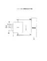
ここで、これら入力バッファ回路41、42、43の動作説明の前に、しきい値が同一の場合の動作について、図2、図3及び図4を参照して説明する。図2は、入力バッファ回路の基本構成を示す回路図、図3は、しきい値が同一の場合の入力電圧及び貫通電流を示す図、図4は、電源回路との関係を示す図である。 Here, before explaining the operation of these
入力バッファ回路41(図2)について、仮に、しきい値電圧Vthが設定されているものとすると、図3の(A)に示すように、しきい値電圧Vthに対し、しきい値電圧Vthより低いレベルからしきい値電圧Vthを超えるレベルまで変化する入力電圧Vinが入力端子61に付与されると、しきい値電圧Vthより低いレベルでトランジスタ411が導通し、しきい値電圧Vthより高いレベルでトランジスタ412が導通状態になる。即ち、入力バッファ回路41では、入力電圧Vinとしきい値電圧Vthとの相対的な関係により電気的な状態変化が生起し、これが出力電圧Voutに現れるが、導通状態の切り換わる時点において、トランジスタ411、412には、図3の(B)に示すように、貫通電流it1が流れる。 Assuming that the threshold voltage Vth is set for the input buffer circuit 41 (FIG. 2), as shown in FIG. When the input voltage Vin changing from a lower level to a level exceeding the threshold voltage Vth is applied to the
この場合、入力バッファ回路42、43にも既述の入力バッファ回路41と同一のしきい値電圧Vthが設定されているものと仮定すると、入力バッファ回路41、42が同時に電気的な状態変化が生起した場合の貫通電流は、入力バッファ回路41の貫通電流it1と入力バッファ回路42の貫通電流it2とが加算された値となる。また、入力バッファ回路41、42、43が同時に電気的な状態変化が生起した場合の貫通電流は、入力バッファ回路41、42、43の貫通電流it1、it2、it3の加算値(it1+it2+it3)となる。 In this case, assuming that the
この場合、しきい値が一致している入力バッファ回路41〜43を含むLSI2では、図4に示すように電源回路14からLSI2に対して貫通電流itが流れ、その値は最大値で、
it=it1+it2+it3 ・・・(1)
となる。この場合、it1=it2=it3とすると、図3の(B)に示すように、it=3it1となり、そのピーク値は入力バッファ回路の設置数Nに比例して増加するとともに、その変化(dit/dt)はその加算値に比例して増加し、これがノイズ発生の要因となり、発生ノイズの振幅を増大させる。In this case, in the
it = it1 + it2 + it3 (1)
It becomes. In this case, if it1 = it2 = it3, as shown in FIG. 3B, it = 3it1, the peak value increases in proportion to the number N of input buffer circuits, and the change (dit) / Dt) increases in proportion to the added value, which causes noise generation and increases the amplitude of the generated noise.
このような動作は、入力電圧Vinが図3の(A)に示すように、時間tの経過とともに増加する場合だけでなく、図3の(A)と全く逆の関係となる、時間tの経過とともに減少する場合でも同様である。これを入力バッファ回路41についてみると、トランジスタ411が遮断状態から導通状態に移行するとともに、トランジスタ412が導通状態から遮断状態に移行する場合である。このような動作は、入力バッファ回路42、43についても同様であり、3つの入力バッファ回路41〜43では、同様に加算された貫通電流(it=3it1)が電源回路14から流れることになる(図4)。 Such an operation is not only in the case where the input voltage Vin increases with the lapse of time t as shown in FIG. 3A, but also at the time t where the relationship is completely opposite to that in FIG. The same applies to the case of decreasing with progress. Looking at this for the
そして、入力バッファ回路41、42、43を構成しているCMOS回路は、信号の切換え時に、即ち、入力電圧Vinが低レベルから増加してしきい値電圧Vthを超える場合、又は、高レベルから減少してしきい値を下回る場合に電流が流れるため、しきい値が同一であれば、貫通電流の立上り(tr)又は立下がり(tf)によって電流の流れる時期が一致する。そこで、同時に入力バッファ回路41、42、43に加えられる複数の入力のそれぞれに対し、入力バッファ回路41、42、43のしきい値が同一であれば、貫通電流が流れる時期が一致し、貫通電流の重畳による電流値が大きくなり、しかも、その変化をその重畳された貫通電流に比例して増加するので、電流変化により発生するノイズ振幅が増強されることになる。ノイズ振幅が大きくなれば、隣接する回路や半導体集積回路に悪影響を及ぼし、誤動作を誘発する原因になる。 The CMOS circuits constituting the
このような電気的な状態変化に起因するノイズ発生等の不都合を回避するには、異なるしきい値を設定し、電気的な状態変化の発生時期を異ならせればよい。そこで、異なるしきい値を設定することにより、ノイズ発生の要因を取り除いたのが、図1に示す入力バッファ回路41、42、43である。 In order to avoid such inconveniences such as noise generation due to the electrical state change, different threshold values may be set and the occurrence timing of the electrical state change may be varied. Therefore, the
次に、異なるしきい値が設定された入力バッファ回路41、42、43の動作について、図5及び図6を参照して説明する。図5は、図1に示す入力バッファ回路の動作を示す図、図6は、入力電圧Vinとしきい値との関係を示す図である。 Next, operations of the
図5の(A)に示すように、入力電圧Vinは時間tの経過に応じてレベルが増加又は減少する変化を持つ電圧である。実線で示す入力電圧Vinは時間tの経過とともに増加する電圧であり、破線で示す入力電圧Vinは時間tの経過とともに減少する電圧である。この入力電圧Vinに対して電源電圧VDD、Vssが設定されており、これら電源電圧VDD、Vssの範囲内にしきい値電圧Vtha、Vthb、Vthcが設定されている。これらしきい値電圧Vtha、Vthb、Vthcは一定の電圧幅を持つ電圧である。 As shown in FIG. 5A, the input voltage Vin is a voltage having a change in which the level increases or decreases with the passage of time t. The input voltage Vin indicated by a solid line is a voltage that increases with the passage of time t, and the input voltage Vin indicated by a broken line is a voltage that decreases with the passage of time t. Power supply voltages VDD and Vss are set for the input voltage Vin, and threshold voltages Vtha, Vthb and Vthc are set within the range of the power supply voltages VDD and Vss. These threshold voltages Vtha, Vthb, and Vthc are voltages having a certain voltage width.
入力端子61、62、63に共通に入力電圧Vinが加えられると、この入力電圧Vinのレベル変化(時間的レベル変化)と、しきい値電圧Vtha、Vthb、Vthcとの相対的な関係により入力バッファ回路41、42、43に電気的な状態変化が生起される。設定されたしきい値電圧Vtha、Vthb、Vthcを異ならせている(この場合、Vtha<Vthb<Vthcである)ことから、生起する電気的な状態変化に時期的な差異が生じている。 When the input voltage Vin is commonly applied to the
具体的には、入力電圧Vinがしきい値電圧Vthaに到達すると、トランジスタ411が導通状態から遮断状態、トランジスタ412が遮断状態から導通状態に遷移し、出力端子81には電気的な状態変化として図5の(B)に示す出力電圧Voutaが生じる。また、入力電圧Vinがしきい値電圧Vthbに到達すると、トランジスタ421が導通状態から遮断状態、トランジスタ422が遮断状態から導通状態に遷移し、出力端子82には電気的な状態変化として図5の(C)に示す出力電圧Voutbが生じる。そして、入力電圧Vinがしきい値電圧Vthcに到達すると、トランジスタ431が導通状態から遮断状態、トランジスタ432が遮断状態から導通状態に遷移し、出力端子83には電気的な状態変化として図5の(D)に示す出力電圧Voutcが生じる。この場合、各入力バッファ回路41、42、43はインバータを構成していることから、入力の反転出力が得られることになる。 Specifically, when the input voltage Vin reaches the threshold voltage Vtha, the
この場合、しきい値電圧Vthaとしきい値電圧Vthbとの電圧差をΔV、しきい値電圧Vthbとしきい値電圧Vthcとの電圧差をΔVとすると、これら電圧差ΔVと入力電圧Vinの時間的レベル変化との相対的な関係から、入力バッファ回路41、42、43に生起する電気的な状態変化の時期がt1、t2、t3のようになり、時間差Δt(t2−t1又はt3−t2)を以て電気的な状態変化が生じる。t1、t2、t3は出力電圧Vouta、Voutb、Voutcの生成タイミングとなる。 In this case, when the voltage difference between the threshold voltage Vtha and the threshold voltage Vthb is ΔV, and the voltage difference between the threshold voltage Vthb and the threshold voltage Vthc is ΔV, the time difference between the voltage difference ΔV and the input voltage Vin is obtained. From the relative relationship with the level change, the timing of the electrical state change occurring in the
ところで、上記説明で参照した図5の(B)〜(E)では入力電圧Vinが時間の経過とともに増加する場合について記載しているが、図5の(A)に破線で示す入力電圧Vinについても同様の動作となる。この場合、トランジスタ411、421、431が遮断状態から導通状態に変化し、トランジスタ412、422、432が導通状態から遮断状態に変化することにより、出力電圧Vouta、Voutb、VoutcがLレベルからHレベルに変化するが、異なるしきい値電圧Vtha、Vthb、Vthcが設定されていることから、入力バッファ回路41、42、43に生起する電気的な状態変化の時期がt1、t2、t3のようになり、これら時期t1、t2、t3が出力電圧Vouta、Voutb、Voutcに生じる状態変化の生成タイミングとなる。 By the way, although (B)-(E) of FIG. 5 referred in the said description has described about the case where input voltage Vin increases with progress of time, about input voltage Vin shown with the broken line in (A) of FIG. Is the same operation. In this case, the
そこで、入力バッファ回路41、42、43に発生する貫通電流をit1、it2、it3とすると、これら貫通電流it1、it2、it3も時期t1、t2、t3に対応し、時間差Δtを以てピーク値を生じる。このため、電源回路14から入力バッファ回路41、42、43に流れ込む各貫通電流it1、it2、it3を加算貫通電流itsは、貫通電流it2のピーク値を中心値とし、貫通電流it1又はit2より僅かに高い2つのピーク値を持つ値となる。従って、全ての入力バッファ回路41、42、43に貫通電流it1、it2、it3が生じても、その値は貫通電流it1又はit2より僅かに高い2つのピーク値を持つにすぎず、その変化(dit/dt)は小さいものとなる。このため、貫通電流itによるノイズの発生が抑えられ、LSI2のノイズによる誤動作を回避することができる。 Therefore, if the through currents generated in the
ここで、入力端子61、62、63に加えられる入力電圧Vinを3ビットのディジタル信号であるとすれば、この場合、入力信号Vinが、「000」、「001」、「010」、「011」、「100」、「101」、「110」、「111」の値を表すことになる。この場合、「0」はVin=低(L)レベル、「1」はVin=高(H)レベルとし、3ビットの最上位桁を入力バッファ回路41の入力端子61に、その中位桁を入力バッファ回路42の入力端子62に、その最下位桁を入力バッファ回路43の入力端子63に対応させると、例えば、入力電圧Vinが「000」から「001」に推移した場合には、最下位桁に対応している入力バッファ回路43の電気的状態が変化する。この場合の貫通電流it3は入力バッファ回路43のみに流れる。また、入力電圧Vinが例えば、「011」から「100」に推移した場合には、最上位桁の「0」は「1」に変化し、中位桁及び最下位桁の「1」は共に「0」に変化しているから、これらに対応して全ての入力バッファ回路41、42、43の電気的状態が変化することになり、貫通電流it1、it2、it3が流れることになる。既述した通り、各貫通電流it1、it2、it3のピーク値は時期的にずれて生じるので、その加算貫通電流itsはそのピーク値が低く抑えられ、しかも、その変化(dis/dt)は小さいものとなり、貫通電流itによるノイズの発生による誤動作を防止できる。 Here, if the input voltage Vin applied to the
ところで、入力端子61、62、63に加えられる入力電圧Vinについて、図6に示すように、入力電圧Vinに時間tbで連続するレベル(電圧段)の電圧Vbを持ち、この電圧Vbがしきい値電圧Vthbに対応している場合には、これに対応する入力バッファ回路42に貫通電流it2が連続して流れることになるが、他の入力バッファ回路41、43には異なるしきい値電圧Vtha、Vthc(≠Vthb)が設定されて状態変化の生起が時期的に異なる。このため、貫通電流it2の影響はなく、加算貫通電流itsのピーク値は低く抑えられ、しかも、その変化(dis/dt)は小さいものとなるから、ノイズが抑制でき、既述の誤動作を防止できる。このような動作は、破線で示す入力電圧Vinの場合にも同様である。 By the way, as shown in FIG. 6, the input voltage Vin applied to the
次に、入力バッファ回路41、42、43に対するしきい値電圧の設定について、図7を参照して説明する。図7は、入力バッファ回路41を構成するCMOS構造を示す断面図である。 Next, the setting of the threshold voltage for the
半導体基板として例えば、シリコン基板16にはn型半導体領域であるnウェル18とp型半導体領域であるpウェル20が隣接して形成され、ツィンウェル構造が形成されている。nウェル18にはp型半導体領域でソース22及びドレイン24が設置され、また、pウェル20にはn型半導体領域でソース26及びドレイン28が設置されている。nウェル18側のドレイン24とpウェル20側のドレイン28との間には分離絶縁領域30がnウェル18とpウェル20に跨がって設置され、この分離絶縁領域30により、各ドレイン24、28間の絶縁が図られている。nウェル18上のソース22とドレイン24の間隔部上には絶縁膜32を介在させてゲート34が設置され、また、pウェル20上のソース26とドレイン28の間隔部上には絶縁膜36を介在させてゲート38が設置されている。 As a semiconductor substrate, for example, an n well 18 that is an n-type semiconductor region and a p well 20 that is a p-type semiconductor region are formed adjacent to each other on a
このようなpn構造により、nウェル18側にはpチャネルのトランジスタ411が構成され、pウェル20側にはnチャネルのトランジスタ412が構成されている。ソース22には電圧VDDを給電する給電端子52、ソース26には電圧Vssを給電する給電端子54が形成されている。 With such a pn structure, a p-
そして、ゲート34、38には共通の配線導体56が接続されて入力端子61が形成され、また、ドレイン24、28には共通の配線導体58が接続されて出力端子81が形成されている。 A
このようなCMOS構造においては、トランジスタ411、412のしきい値電圧Vthaは、基板領域におけるnウェル18及びpウェル20の不純物濃度によって決定されるので、その不純物濃度の制御により、所望の電圧値に設定することができる。pウェル20側に形成されるnチャネルのトランジスタ412は、pウェル20の不純物濃度を上げることにより、しきい値Vthaを上昇させることができる。 In such a CMOS structure, the threshold voltage Vtha of the
また、このようなCMOS構造においては、トランジスタ411、412におけるチャネルは、絶縁膜32、36の膜厚dにより、しきい値電圧Vthaを変えることができる。そこで、絶縁膜32、36の膜厚dの設定により、所望のしきい値電圧Vthaに設定することができる。 In such a CMOS structure, the threshold voltage Vtha of the channels in the
このようなしきい値電圧Vthaの設定については、同様のCMOS構造で入力バッファ回路42、43を構成するのであれば、同様にそれらのしきい値電圧Vthb、Vthcを設定することができる。即ち、CMOS構造における、nウェル18、pウェル20の不純物濃度や絶縁膜32、36の膜厚d等の定数設定により、所望のしきい値電圧Vtha、Vthb、Vthcを設定でき、そのレベル値をVtha<Vthb<Vthcに設定することができる。 With respect to the setting of the threshold voltage Vtha, the threshold voltages Vthb and Vthc can be similarly set if the
第2の実施の形態 Second embodiment
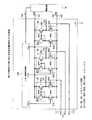
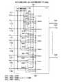
次に、本発明の第2の実施の形態について、図8を参照して説明する。図8は、異なるしきい値を持つ入力バッファ回路が搭載されたLSIの構成例を示す図である。 Next, a second embodiment of the present invention will be described with reference to FIG. FIG. 8 is a diagram illustrating a configuration example of an LSI on which input buffer circuits having different threshold values are mounted.
このLSI2では、異なるしきい値を持つ複数の入力バッファ回路ブロックとして例えば、3組の入力バッファ回路ブロック410、420、430が設置され、各入力バッファ回路ブロック410、420、430は複数の入力バッファとして例えば、入力バッファ回路4101、4102・・・410N、入力バッファ回路4201、4202・・・420N、入力バッファ回路4301、4302・・・430Nで構成されている。この実施の形態では、入力バッファ回路ブロック410にはしきい値電圧Vtha、入力バッファ回路ブロック420にはしきい値電圧Vthb、入力バッファ回路ブロック430にはしきい値電圧Vthcが設定されている。これらしきい値電圧Vtha、Vthb、Vthcの大小関係は例えば、Vtha<Vthb<Vthcである。 In this
要するに、このLSI2に関し、言い換えれば、各入力バッファ回路ブロック410、420、430は、共通のタイミングで入力電圧Vinを受けて状態変化を呈する入力バッファ回路4101、4102・・・410N、4201、4202・・・420N、4301、4302・・・430Nについて、異なるしきい値電圧Vtha、Vthb、Vthcを個別に設定してグルーピング化されたものである。即ち、共通のしきい値電圧Vthaが設定された入力バッファ回路4101、4102・・・410Nを入力バッファ回路ブロック410、共通のしきい値電圧Vthbが設定された入力バッファ回路4201、4202・・・420Nを入力バッファ回路ブロック420、共通のしきい値電圧Vthcが設定された入力バッファ回路4301、4302・・・430Nを入力バッファ回路ブロック430としたものである。 In short, regarding this
そして、このLSI2では、入力端子611、612・・・61N、621、622・・・62N、631、632・・・63Nには、複数ビットのディジタル信号等の入力として例えば、入力電圧Vinが加えられ、各入力バッファ回路ブロック410、420、430には出力電圧Vouta、Voutb、Voutcが得られ、また、出力端子71、72・・7Nから出力電圧Voが得られる。 In this
斯かる構成とすれば、図5の(A)に示すように、入力端子611、612・・・61N、621、622・・・62N、631、632・・・63Nに共通に入力電圧Vinが加えられると、この入力電圧Vinと、しきい値電圧Vtha、Vthb、Vthcとの大小関係により、入力バッファ回路ブロック410、420、430に電気的な状態変化が生起される。設定されたしきい値電圧Vtha、Vthb、Vthcを異ならせているので、生起する電気的な状態変化に時期的な差異が生じる。 With such a configuration, as shown in FIG. 5A, the input voltage Vin is common to the
具体的には、入力電圧Vinがしきい値電圧Vthaに到達すると、入力バッファ回路ブロック410の各入力バッファ回路4101〜410Nに状態変化が生起され、また、入力電圧Vinがしきい値電圧Vthbに到達すると、入力バッファ回路ブロック420の各入力バッファ回路4201〜420Nに状態変化が生起され、また、入力電圧Vinがしきい値電圧Vthcに到達すると、入力バッファ回路ブロック430の各入力バッファ回路4301〜430Nに状態変化が生起される。即ち、入力バッファ回路ブロック410、420、430は共通の入力電圧Vinを受けながら、しきい値電圧Vtha、Vthb、Vthcが異なるため、生起する状態変化のタイミングが相違することになる。この点は、図5の(B)、(C)、(D)に示した通りである。 Specifically, when the input voltage Vin reaches the threshold voltage Vtha, a state change occurs in each of the
このような状態変化により、入力バッファ回路ブロック410、420、430に発生する貫通電流をit10、it20、it30とすると、これら貫通電流it10、it20、it30も時期t1、t2、t3に対応し、既述した時間差Δt(図5)を以てピーク値を生じることになる。また、電源回路14から入力バッファ回路ブロック410、420、430の各貫通電流をit10、it20、it30を加算貫通電流its0は、図5の(E)と同様の形態となり、そのピーク値が低く抑えられ、その変化も小さいものとなるから、貫通電流it0によるノイズの発生が抑えられ、LSI2のノイズによる誤動作を回避することができる。 When the through currents generated in the input buffer circuit blocks 410, 420, and 430 due to such a state change are it10, it20, and it30, these through currents it10, it20, and it30 also correspond to the times t1, t2, and t3, The peak value is generated with the time difference Δt (FIG. 5) described above. Further, the through current from the
第3の実施の形態 Third embodiment
次に、本発明の第3の実施の形態について、図9、図10及び図11を参照して説明する。図9は、異なるしきい値を持つ複数の入力バッファ回路が搭載されたLSI2の構成例を示す回路図、図10は、各入力バッファ回路の構成例を示す回路図、図11は、しきい値設定回路の構成例を示す回路図である。 Next, a third embodiment of the present invention will be described with reference to FIG. 9, FIG. 10, and FIG. 9 is a circuit diagram showing a configuration example of the
LSI等の半導体集積回路に関し、素子やインバータ等の回路にしきい値の設定は既述した素子構成の定数設定の他、電子回路の回路構成によっても達成することができる。そこで、この実施の形態では、各入力バッファ回路91、92、93には、電子回路の回路構成によって異なるしきい値電圧Vtha、Vthb、Vthcが設定されており、そのしきい値電圧Vtha、Vthb、Vthcの設定のために、しきい値設定回路100が設置されている。 Regarding a semiconductor integrated circuit such as an LSI, setting of a threshold value in a circuit such as an element or an inverter can be achieved not only by the constant setting of the element configuration described above but also by the circuit configuration of an electronic circuit. In this embodiment, therefore, different threshold voltages Vtha, Vthb, Vthc are set in the
このLSI2において、入力バッファ回路91はトランジスタ911、912、913、914で構成されている。トランジスタ911、913はpチャネルMOSトランジスタで構成され、トランジスタ912、914はnチャネルMOSトランジスタで構成されており、トランジスタ911、912はCMOS回路を構成し、同様に、トランジスタ913、914もCMOS回路を構成している。トランジスタ912のゲートには入力端子111が形成されて入力電圧Vinが加えられ、また、トランジスタ914のゲートにはしきい値電圧Vtha(又はVthb、Vthc)がしきい値設定回路100から加えられる。また、各トランジスタ911、912の共通接続されたドレインには出力端子121が形成されて出力電圧Voutaが取り出される。また、トランジスタ911、913のソースには給電端子141に接続された電源回路14から電圧VDDが加えられ、トランジスタ912、914のソースは接地端子142を通して接地点(GND)に接続されている。 In this
また、入力バッファ回路92はトランジスタ921、922、923、924で構成されており、また、入力バッファ回路93はトランジスタ931、932、933、934で構成されており、しきい値電圧Vthb、Vthcが相違し、それに応じて出力電圧Voutb、Voutcが取り出されるが、これらの素子の構成及び接続、電源回路14及びしきい値設定回路100との接続関係は入力バッファ回路91と同様である。 The
そして、しきい値設定回路100は例えば、図11に示すように、抵抗101、102、103、104を以て分圧回路105を構成することにより、給電端子143を通して電源回路14より加えられる一定電圧Vrを分圧することにより、異なるしきい値電圧Vtha、Vthb、Vthcを得ることができる。 For example, as shown in FIG. 11, the
斯かる構成とすれば、図5の(A)に示すように、入力端子111、112、113に共通に入力電圧Vinが加えられると、この入力電圧Vinと、しきい値電圧Vtha、Vthb、Vthcとの大小関係により、入力バッファ回路91、92、93に電気的な状態変化が生起され、設定されたしきい値電圧Vtha、Vthb、Vthcを異ならせているので、生起する状態変化に時期的な差異が生じる。 With this configuration, as shown in FIG. 5A, when the input voltage Vin is commonly applied to the
斯かる入力バッファ回路91、92、93について、しきい値電圧Vtha、Vthb、Vthcの設定と、入力電圧Vinを受けた際に生起する状態変化に時期的な差異が生じることについて、図10を参照して説明する。 Regarding such
図10に示すように、入力バッファ回路91において、トランジスタ911のゲートとトランジスタ913のゲート及びドレインとは共通に接続されているので、トランジスタ911、913はカレントミラー回路144を構成している。また、トランジスタ912、914の各ソースは共通の接地点に接続していることから、トランジスタ912、914は差動対146を構成している。従って、カレントミラー回路144は、差動対146に対して負荷を構成している。 As shown in FIG. 10, in the
説明を容易にするため、この入力バッファ回路91のトランジスタ914に対し、しきい値設定回路100(図11)により異なるしきい値電圧Vtha、Vthb、Vthcの何れかが加えられるものとする。 For ease of explanation, it is assumed that any one of threshold voltages Vtha, Vthb, and Vthc is applied to the
そこで、トランジスタ914に例えば、しきい値電圧Vthaが設定された場合であって、入力電圧Vinがしきい値電圧Vthaより低いか又はVin=0の場合には、設定されているしきい値電圧Vthaに対応してトランジスタ914が導通状態となる。この導通により、トランジスタ911、913は、各ゲートがトランジスタ914を通して接地電位に低下するため、共に導通状態となる。この結果、トランジスタ913、914にはトランジスタ914のゲートに設定されたしきい値電圧Vthaに応じた電流が流れ、出力端子121にはしきい値電圧Vthaに応じた高(H)レベルの出力電圧Voutaが得られる。 Therefore, for example, when the threshold voltage Vtha is set in the
また、入力電圧Vinがしきい値電圧Vthaより高い(H)場合には、トランジスタ912が導通状態になって、トランジスタ911は遮断状態に陥るとともに、出力端子121の出力電圧Voutaは、低(L)レベルに立ち下がる。このとき、トランジスタ913、914も同様に、導通状態から遮断状態に遷移する。 When the input voltage Vin is higher than the threshold voltage Vtha (H), the
このような状態変化は、しきい値電圧Vthb、Vthcが設定されている場合でも同様であり、異なる点は、入力電圧Vinとしきい値電圧Vtha、Vthb、Vthcとの関係から、導通タイミングに相違が生じることである。即ち、図5に示すように、入力電圧Vinのレベル変化がしきい値電圧Vtha、Vthb、Vthcに到達した時点t1、t2、t3で状態変化が生じ、トランジスタ911、912に貫通電流it1が流れることになる。 This state change is the same even when the threshold voltages Vthb and Vthc are set. The difference is that the conduction timing is different from the relationship between the input voltage Vin and the threshold voltages Vtha, Vthb, and Vthc. Will occur. That is, as shown in FIG. 5, the state change occurs at time points t1, t2, and t3 when the level change of the input voltage Vin reaches the threshold voltages Vtha, Vthb, and Vthc, and the through current it1 flows through the
このような動作を異なるしきい値電圧Vtha、Vthb、Vthcが設定された入力バッファ回路91、92、93(図9)に当てはめると、共通の入力電圧Vinを受けても、異なるしきい値電圧Vtha、Vthb、Vthcにより、導通タイミングが相違することになり、電源回路14から各入力バッファ回路91、92、93に流れる貫通電流it1、it2、it3は時期的に異なり、そのピーク値の重畳が回避される。この結果、同時にトランジスタ911、921、931が導通しても、貫通電流のピーク値が低く抑えられ、しかも、その変化が抑制されるので、貫通電流によるノイズの発生が抑えられ、LSI2のノイズによる誤動作を回避することができる。 When such an operation is applied to the
このように異なるしきい値電圧Vtha、Vthb、Vthcは、図9に示すように、回路構成によっても、同様に設定することができ、貫通電流の発生タイミングを異ならせることができる。 As shown in FIG. 9, the different threshold voltages Vtha, Vthb, and Vthc can be set similarly depending on the circuit configuration, and the generation timing of the through current can be varied.
また、この実施の形態では、LSI2の内部回路としてしきい値設定回路100を設置したが、図12に示すように、LSI2の外部回路としてしきい値設定回路100を構成しても同様の機能が得られる。 In this embodiment, the
第4の実施の形態 Fourth embodiment
次に、本発明の第4の実施の形態について、図13を参照して説明する。図13は、しきい値設定回路を以て異なるしきい値が設定された入力バッファ回路を搭載したLSIの構成例を示す図である。 Next, a fourth embodiment of the present invention will be described with reference to FIG. FIG. 13 is a diagram illustrating a configuration example of an LSI equipped with an input buffer circuit in which different threshold values are set by the threshold value setting circuit.
このLSI2では、異なるしきい値を持つ複数の入力バッファ回路ブロックとして例えば、3組の入力バッファ回路ブロック910、920、930が設置され、各入力バッファ回路ブロック910、920、930は複数の入力バッファとして例えば、入力バッファ回路9101、9102・・・910N、入力バッファ回路9201、9202・・・920N、入力バッファ回路9301、9302・・・930Nで構成されている。この実施の形態では、共通のしきい値設定回路100を以て入力バッファ回路ブロック910にはしきい値電圧Vtha、入力バッファ回路ブロック920にはしきい値電圧Vthb、入力バッファ回路ブロック930にはしきい値電圧Vthcが設定されている。Vtha、Vthb、Vthcは例えば、Vtha<Vthb<Vthcである。 In this
そして、入力端子1111、1112・・・111N、1121、1122・・・112N、1131、1132・・・113Nには、複数ビットのディジタル信号等の入力として例えば、入力電圧Vinが加えられ、各入力バッファ回路ブロック910、920、930には出力電圧Vouta、Voutb、Voutcが得られ、また、出力端子1481、1482・・・148Nから出力電圧Voが得られる。 The
斯かる構成とすれば、図5の(A)に示すように、入力端子1111〜111N、1121〜112N、1131〜113Nに共通に入力電圧Vinが加えられると、この入力電圧Vinと、しきい値電圧Vtha、Vthb、Vthcとの大小関係により、入力バッファ回路ブロック910、920、930に電気的な状態変化が生起される。設定されたしきい値電圧Vtha、Vthb、Vthcを異ならせているので、生起する電気的な状態変化に時期的な差異が生じる。 With such a configuration, as shown in FIG. 5A, when the input voltage Vin is commonly applied to the
具体的には、入力電圧Vinがしきい値電圧Vthaに到達すると、入力バッファ回路ブロック910の各入力バッファ回路9101〜910Nに状態変化が生起され、また、入力電圧Vinがしきい値電圧Vthbに到達すると、入力バッファ回路ブロック920の各入力バッファ回路9201〜920Nに状態変化が生起され、また、入力電圧Vinがしきい値電圧Vthcに到達すると、入力バッファ回路ブロック930の各入力バッファ回路9301〜930Nに状態変化が生起される。これは、図5の(B)、(C)、(D)に示した通りである。 Specifically, when the input voltage Vin reaches the threshold voltage Vtha, a state change occurs in each of the
斯かる状態変化により、入力バッファ回路ブロック910、920、930に発生する貫通電流をit10、it20、it30とすると、これら貫通電流it10、it20、it30も時期t1、t2、t3に対応し、既述した時間差Δt(図5)を以てピーク値を生じることになる。また、電源回路14から入力バッファ回路ブロック910、920、930の各貫通電流をit10、it20、it30を加算貫通電流its0は、図5の(E)と同様の形態となり、そのピーク値が低く抑えられ、その変化も小さいものとなる。この結果、貫通電流it0によるノイズの発生が抑えられ、LSI2のノイズによる誤動作を回避することができる。 When the through current generated in the input buffer circuit blocks 910, 920, and 930 is assumed to be it10, it20, and it30 due to such a state change, the through currents it10, it20, and it30 also correspond to the times t1, t2, and t3. The peak value is generated with the time difference Δt (FIG. 5). In addition, the through current from the
なお、この実施の形態では、しきい値設定回路100をLSI2の内部回路で構成したが、図12に示すようにLSI2の外部回路で構成しても同様の機能が得られる。 In this embodiment, the
第5の実施の形態 Fifth embodiment
次に、本発明の第5の実施の形態について、図14を参照して説明する。図14は、しきい値の異なる入力バッファ回路の搭載例であるLSIを示す図である。 Next, a fifth embodiment of the present invention will be described with reference to FIG. FIG. 14 is a diagram illustrating an LSI as an example of mounting input buffer circuits having different threshold values.
このLSI2はメモリLSIの一例であって、このLSI2には記憶装置として複数のメモリセルアレイ(MEMORY CELL ARRAY)150、151、152、153が設置されている。メモリセルアレイ150〜153はバンク0〜バンク3を構成している。メモリセルアレイ150〜153に対応し、ローデコーダ(ROW DECODER)160、161、162、163、センスアンプ(SENSE AMP.)170、171、172、173及びコラムデコーダ(COLUMN DECODER)180、181、182、183が設置されている。センスアンプ(SENSE AMP.)170、171、172、173は、データ信号の増幅のために設置されている。 The
また、ローデコーダ160〜163側には、ローアドレスバッファ及びリフレッシュカウンタ(ROW ADDRESS BUFFER AND REFRESH COUNTER)200、コラムデコーダ180〜183側には、コラムアドレスバッファ及びバーストカウンタ(COLUMN ADDRESS BUFFER AND BURST COUNTER)202が設置され、このローアドレスバッファ及びリフレッシュカウンタ200及びコラムアドレスバッファ及びバーストカウンタ202には、複数の入力ピンA0−A12、BA0、BA1を以てアドレスデータが付与される。また、入力ピン204からのアドレスデータはモードレジスタ(MODE REGISTER)206にも加えられている。入力ピンBA0、BA1に加えられる2ビットのディジタル信号により、BANK0〜3を構成するメモリセルアレイ150〜153が選択される。 Further, a row address buffer and refresh counter (ROW ADDRESS BUFFER AND REFRESH COUNTER) 200 is provided on the
また、コラムデコーダ180〜183には入出力バッファ(INPUT AND OUTPUT BUFFER)208、ラッチ回路(LATCH CIRCUIT)210、データコントロール回路(DATA CONTROL CIRCUIT)212が設置されている。入出力バッファ208には位相調整のためのDLL(Dalay Locked Loop )214が併設されている。入出力バッファ208はデータ入出力ピン(DQ、DQ0−DQ15)216を通してデータの入出力が行われる。 The column decoders 180 to 183 are provided with an input / output buffer (INPUT AND OUTPUT BUFFER) 208, a latch circuit (LATCH CIRCUIT) 210, and a data control circuit (DATA CONTROL CIRCUIT) 212. The input /
その他、コマンドデコーダ(COMMAND DECODER)218、コントロールロジック回路(CONTROL LOGIC)220及びクロック発振器(CLOCK GENERATOR)222が設置されている。コマンドデコーダ218には複数の入力データとしてチップセレクト(Chip Select )信号/CS、ローアドレス(Row Address )信号/RAS、コラムアドレス(Column Address)信号/CAS、ライトイネーブル(Write Enable)信号(W/WE)が加えられ、これらに対応した入力バッファ回路が設置されている。 In addition, a command decoder (COMMAND DECODER) 218, a control logic circuit (CONTROL LOGIC) 220, and a clock oscillator (CLOCK GENERATOR) 222 are provided. The
このようなメモリLSIを構成しているLSI2において、入力ピン204に接続されるローアドレスバッファ及びリフレッシュカウンタ200、コラムアドレスバッファ及びバーストカウンタ202における入力バッファ回路、入出力ピン216に接続される入出力バッファ208における入力バッファ回路、出力バッファ回路について、異なるしきい値を設定してブロック化すれば、既述の通り、しきい値電圧を異ならせたことによる導通タイミングを異ならせ、貫通電流のピーク値の重畳を防止できるとともに、その変化を抑制することができる。 In the
また、入力ピン204におけるデータ(A0−A12)やデータ入出力ピン(DQ)216を通してデータ入力DQ0−DQ15を適宜に分割し、その入力バッファ回路又は出力バッファ回路のしきい値を異ならせて複数の値を設定すればよい。例えば、入力データ(DQ0−DQ15)に対し、入力データ(DQ0−DQ7)に対応する入力バッファ回路のしきい値電圧Vtha、入力データ(DQ8−DQ15)に対応する入力バッファ回路のしきい値電圧Vthbを設定して分割すれば、貫通電流のピーク値の重畳を避けることができ、その変化を抑制できる。従って、貫通電流によるノイズやその影響を回避し、LSI2の誤動作を回避することができる。 Further, the data inputs DQ0 to DQ15 are appropriately divided through the data (A0 to A12) and the data input / output pins (DQ) 216 at the input pins 204, and the thresholds of the input buffer circuit or the output buffer circuit are made different. Should be set. For example, for input data (DQ0-DQ15), the threshold voltage Vtha of the input buffer circuit corresponding to the input data (DQ0-DQ7), the threshold voltage of the input buffer circuit corresponding to the input data (DQ8-DQ15) If Vthb is set and divided, the peak value of the through current can be prevented from being superimposed, and the change can be suppressed. Therefore, noise due to the through current and its influence can be avoided, and malfunction of the
他の実施の形態 Other embodiments
次に、他の実施の形態及びその特徴事項等を以下に列挙する。 Next, other embodiments and their features are listed below.
(1) 上記実施の形態では、入力バッファ回路を例示したが、同一構成で出力バッファ回路として構成し、異なるしきい値を設定すれば、同様に、貫通電流のピーク値の重畳を防止でき、その変化を抑制することができる。その結果、ノイズ発生やその影響を回避でき、LSIの誤動作を防止できる。 (1) In the above embodiment, the input buffer circuit is exemplified, but if it is configured as an output buffer circuit with the same configuration and different threshold values are set, similarly, it is possible to prevent the peak value of the through current from being superimposed, The change can be suppressed. As a result, noise generation and its influence can be avoided, and malfunction of the LSI can be prevented.
(2) 上記実施の形態では、CMOS回路を例示したが、本発明は、CMOS回路以外のインバータやスイッチング回路に適用することができ、CMOS回路に限定されるものではない。 (2) Although the CMOS circuit has been exemplified in the above embodiment, the present invention can be applied to inverters and switching circuits other than the CMOS circuit, and is not limited to the CMOS circuit.
(3) 入力によって状態変化を呈する素子又は回路として、FETやCMOS回路を例示したが、入力によって状態変化を呈する素子又は回路には、バイポーラトランジスタやそのバイポーラトランジスタを用いたインバータ回路等の各種の素子や回路を含むものである。 (3) The FET or CMOS circuit is exemplified as an element or circuit that exhibits a state change by input, but various elements such as a bipolar transistor or an inverter circuit using the bipolar transistor may be used for the element or circuit that exhibits a state change by an input. It includes elements and circuits.
(4) 上記実施の形態では、複数の素子又は回路を含む半導体集積回路において、異なるしきい値として3種のしきい値電圧Vtha、Vthb、Vthcを設定した場合を説明したが、このしきい値電圧の設定数は3以下でもよく、4以上でもよい。このしきい値の設定については、入力電圧のレベル変化等の入力条件、入力バッファ回路の動作周波数、駆動電圧等の回路条件によって設定すればよい。また、しきい値電圧の設定数を増加すれば、その分だけ素子又は回路の状態変化の時期が異なってくるので、回路機能を損なわない範囲で任意に設定すればよい。 (4) In the above embodiment, the case where three threshold voltages Vtha, Vthb, and Vthc are set as different threshold values in a semiconductor integrated circuit including a plurality of elements or circuits has been described. The number of value voltages set may be 3 or less, or 4 or more. The threshold value may be set according to input conditions such as a change in input voltage level, circuit conditions such as an operating frequency of the input buffer circuit, and a driving voltage. Further, if the set number of threshold voltages is increased, the timing of the state change of the element or circuit differs accordingly, so it may be set arbitrarily within a range that does not impair the circuit function.
次に、以上述べた本発明の半導体集積回路及びそのノイズ低減方法の各実施形態から抽出される技術的思想を請求項の記載形式に準じて付記として列挙する。本発明に係る技術的思想は上位概念から下位概念まで、様々なレベルやバリエーションにより把握できるものであり、以下の付記に本発明が限定されるものではない。 Next, technical ideas extracted from the embodiments of the semiconductor integrated circuit and the noise reduction method thereof according to the present invention described above are listed as appendices according to the description format of the claims. The technical idea according to the present invention can be grasped by various levels and variations from a superordinate concept to a subordinate concept, and the present invention is not limited to the following supplementary notes.
(付記1) しきい値を異ならせた複数の素子又は回路を含み、これら素子又は回路に共通の入力が同時に加えられた場合に、前記しきい値に応じて異なる時期に状態変化を生じる構成としたことを特徴とする半導体集積回路。 (Supplementary Note 1) Configuration including a plurality of elements or circuits having different threshold values, and when a common input is simultaneously applied to these elements or circuits, a state change occurs at different times according to the threshold values A semiconductor integrated circuit characterized by the above.
(付記2) 前記素子は、トランジスタであることを特徴とする付記1記載の半導体集積回路。 (Additional remark 2) The said element is a transistor, The semiconductor integrated circuit of
(付記3) 前記回路は、CMOS回路であることを特徴とする付記1記載の半導体集積回路。 (Additional remark 3) The said circuit is a CMOS circuit, The semiconductor integrated circuit of
(付記4) 前記しきい値は、前記素子又は前記回路が持つ定数により設定してなることを特徴とする付記1記載の半導体集積回路。 (Additional remark 4) The said threshold value is set with the constant which the said element or the said circuit has, The semiconductor integrated circuit of
(付記5) 複数の素子又は回路を含む半導体集積回路のノイズ低減方法であって、
前記素子又は回路に異なるしきい値を設定し、
同時に共通の入力を受けた場合に、前記しきい値に応じて異なる時期に状態変化を生じさせることを特徴とする半導体集積回路のノイズ低減方法。(Supplementary Note 5) A noise reduction method for a semiconductor integrated circuit including a plurality of elements or circuits,
Set different thresholds for the element or circuit,
A method for reducing noise in a semiconductor integrated circuit, wherein when a common input is received simultaneously, a state change is caused at different times according to the threshold value.
(付記6) 前記しきい値は、前記素子の基板領域の不純物濃度により設定されていることを特徴とする付記1又は2記載の半導体集積回路。 (Supplementary note 6) The semiconductor integrated circuit according to
(付記7) 前記しきい値は、前記素子のチャネルが形成される基板領域と、前記素子のゲートとの距離により設定されていることを特徴とする付記1又は2記載の半導体集積回路。 (Supplementary note 7) The semiconductor integrated circuit according to
(付記8) 前記素子又は前記回路に異なるしきい値を設定するしきい値設定回路を備える構成としたことを特徴とする付記1又は2記載の半導体集積回路。 (Supplementary note 8) The semiconductor integrated circuit according to
(付記9) 入力に応じて状態変化を生じる複数の回路を含む半導体集積回路であって、
前記回路が、
異なるしきい値電圧が入力される第1のトランジスタと入力電圧が加えられる第2のトランジスタとからなる複数の差動対と、
前記各差動対毎に前記第1のトランジスタ及び前記第2のトランジスタの負荷を構成するカレントミラー回路と、
を含むことを特徴とする半導体集積回路。(Supplementary Note 9) A semiconductor integrated circuit including a plurality of circuits that change state in response to an input,
The circuit is
A plurality of differential pairs consisting of a first transistor to which a different threshold voltage is input and a second transistor to which the input voltage is applied;
A current mirror circuit constituting a load of the first transistor and the second transistor for each differential pair;
A semiconductor integrated circuit comprising:
(付記10) 入力に応じて状態変化を生じる複数のCMOS回路を含む半導体集積回路であって、
異なるしきい値が設定され、同時に共通の入力を受けた場合に、前記しきい値の相違に応じて異なる時期に状態変化を生起する単一又は複数のCMOS回路を含むことを特徴とする半導体集積回路。(Supplementary Note 10) A semiconductor integrated circuit including a plurality of CMOS circuits that change state in response to an input,
A semiconductor device including a single or a plurality of CMOS circuits that cause a state change at different times according to a difference in the threshold value when different threshold values are set and a common input is received at the same time Integrated circuit.
(付記11) 入力に応じて状態変化を生じる複数のCMOS回路を含む半導体集積回路であって、
異なるしきい値が設定され、同時に共通の入力を受けた場合に、前記しきい値の相違に応じて貫通電流の立上り又は立下りの時期を異ならせ、素子間に流れる貫通電流のピーク値の重畳を回避した単一又は複数のCMOS回路を含むことを特徴とする半導体集積回路。(Supplementary Note 11) A semiconductor integrated circuit including a plurality of CMOS circuits that change state in response to an input,
When different threshold values are set and a common input is received at the same time, the rising or falling timing of the through current is changed according to the difference in the threshold value, and the peak value of the through current flowing between the elements is changed. A semiconductor integrated circuit comprising a single or a plurality of CMOS circuits avoiding superposition.
以上説明したように、本発明の最も好ましい実施形態等について説明したが、本発明は、上記記載に限定されるものではなく、特許請求の範囲に記載され、又は明細書に開示された発明の要旨に基づき、当業者において様々な変形や変更が可能であることは勿論であり、斯かる変形や変更が、本発明の範囲に含まれることは言うまでもない。
As described above, the most preferable embodiment of the present invention has been described. However, the present invention is not limited to the above description, and is described in the claims or disclosed in the specification. It goes without saying that various modifications and changes can be made by those skilled in the art based on the gist, and such modifications and changes are included in the scope of the present invention.
本発明は、半導体集積回路にしきい値を異ならせた複数の素子又は回路を含む構成としたことから、共通の入力が同時に加えられた場合に、前記しきい値に応じて異なる時期に状態変化を生じるので、状態変化による電流が重畳されるのを回避でき、その電流によるノイズ発生又はその振幅を低減でき、半導体集積回路の誤動作防止とともに、信頼性の向上を図ることができ、有用である。
In the present invention, since the semiconductor integrated circuit includes a plurality of elements or circuits having different threshold values, when a common input is applied simultaneously, the state changes at different times according to the threshold values. Therefore, it is possible to avoid the superposition of the current due to the state change, to reduce the noise generation or the amplitude due to the current, to prevent malfunction of the semiconductor integrated circuit, and to improve the reliability, which is useful. .
2 LSI
14 電源回路
41、42、43、4101、4102・・・410N、4201、4202・・・420N、4301、4302・・・430N、91、92、93、9101、9102・・・910N、9201、9202・・・920N、9301、9302・・・930N 入力バッファ回路
410、420、430 入力バッファ回路ブロック
411、421、431 第1のトランジスタ
412、422、432 第2のトランジスタ
911、912、913、914、921、922、923、924、931、932、933、934 トランジスタ
100 しきい値設定回路
22、26 ソース
24、28 ドレイン
34、38 ゲート
32、36 絶縁膜2 LSI
14
Claims (5)
Translated fromJapanese前記素子又は回路に異なるしきい値を設定し、
同時に共通の入力を受けた場合に、前記しきい値に応じて異なる時期に状態変化を生じさせることを特徴とする半導体集積回路のノイズ低減方法。A method for reducing noise in a semiconductor integrated circuit including a plurality of elements or circuits,
Set different thresholds for the element or circuit,
A method for reducing noise in a semiconductor integrated circuit, wherein when a common input is received simultaneously, a state change is caused at different times according to the threshold value.
Priority Applications (3)
| Application Number | Priority Date | Filing Date | Title |
|---|---|---|---|
| JP2005080702AJP2006262421A (en) | 2005-03-18 | 2005-03-18 | Semiconductor integrated circuit and noise reduction method thereof |
| US11/178,371US20060208772A1 (en) | 2005-03-18 | 2005-07-12 | Semiconductor integrated circuit and noise-reduction method thereof |
| KR1020050069293AKR20060101163A (en) | 2005-03-18 | 2005-07-29 | Semiconductor integrated circuit and noise reduction method thereof |
Applications Claiming Priority (1)
| Application Number | Priority Date | Filing Date | Title |
|---|---|---|---|
| JP2005080702AJP2006262421A (en) | 2005-03-18 | 2005-03-18 | Semiconductor integrated circuit and noise reduction method thereof |
Publications (1)
| Publication Number | Publication Date |
|---|---|
| JP2006262421Atrue JP2006262421A (en) | 2006-09-28 |
Family
ID=37009664
Family Applications (1)
| Application Number | Title | Priority Date | Filing Date |
|---|---|---|---|
| JP2005080702AWithdrawnJP2006262421A (en) | 2005-03-18 | 2005-03-18 | Semiconductor integrated circuit and noise reduction method thereof |
Country Status (3)
| Country | Link |
|---|---|
| US (1) | US20060208772A1 (en) |
| JP (1) | JP2006262421A (en) |
| KR (1) | KR20060101163A (en) |
Families Citing this family (7)
| Publication number | Priority date | Publication date | Assignee | Title |
|---|---|---|---|---|
| US7845537B2 (en) | 2006-01-31 | 2010-12-07 | Ethicon Endo-Surgery, Inc. | Surgical instrument having recording capabilities |
| US9307989B2 (en) | 2012-03-28 | 2016-04-12 | Ethicon Endo-Surgery, Llc | Tissue stapler having a thickness compensator incorportating a hydrophobic agent |
| US9232941B2 (en) | 2010-09-30 | 2016-01-12 | Ethicon Endo-Surgery, Inc. | Tissue thickness compensator comprising a reservoir |
| US9314246B2 (en) | 2010-09-30 | 2016-04-19 | Ethicon Endo-Surgery, Llc | Tissue stapler having a thickness compensator incorporating an anti-inflammatory agent |
| US9301753B2 (en) | 2010-09-30 | 2016-04-05 | Ethicon Endo-Surgery, Llc | Expandable tissue thickness compensator |
| US10199334B2 (en)* | 2015-10-20 | 2019-02-05 | Infineon Technologies Ag | Digital circuit and method for manufacturing a digital circuit |
| DE102019123555B4 (en) | 2019-09-03 | 2022-12-01 | Infineon Technologies Ag | PHYSICALLY OBFUSCED CIRCUIT |
Family Cites Families (8)
| Publication number | Priority date | Publication date | Assignee | Title |
|---|---|---|---|---|
| KR100254134B1 (en)* | 1991-11-08 | 2000-04-15 | 나시모토 류우조오 | Semiconductor integrated circuit having current reduction circuit in the standby state |
| US5614847A (en)* | 1992-04-14 | 1997-03-25 | Hitachi, Ltd. | Semiconductor integrated circuit device having power reduction mechanism |
| JPH06208790A (en)* | 1993-01-12 | 1994-07-26 | Toshiba Corp | Semiconductor device |
| US5426376A (en)* | 1993-04-23 | 1995-06-20 | Vlsi Technology, Inc. | Noise isolated I/O buffer that uses two separate power supplies |
| US5559465A (en)* | 1994-07-29 | 1996-09-24 | Cypress Semiconductor Corporation | Output preconditioning circuit with an output level latch and a clamp |
| US5739700A (en)* | 1996-09-09 | 1998-04-14 | International Business Machines Corporation | Method and apparatus with dual circuitry for shifting the level of a signal |
| US6157222A (en)* | 1999-03-29 | 2000-12-05 | Texas Instruments Incorporated | Low power adjustable input threshold circuit |
| JP3579633B2 (en)* | 2000-05-19 | 2004-10-20 | 株式会社ルネサステクノロジ | Semiconductor integrated circuit |
- 2005
- 2005-03-18JPJP2005080702Apatent/JP2006262421A/ennot_activeWithdrawn
- 2005-07-12USUS11/178,371patent/US20060208772A1/ennot_activeAbandoned
- 2005-07-29KRKR1020050069293Apatent/KR20060101163A/ennot_activeCeased
Also Published As
| Publication number | Publication date |
|---|---|
| KR20060101163A (en) | 2006-09-22 |
| US20060208772A1 (en) | 2006-09-21 |
Similar Documents
| Publication | Publication Date | Title |
|---|---|---|
| JP5624441B2 (en) | Semiconductor device | |
| KR900008439B1 (en) | Buffer Circuit in Integrated Circuit | |
| JP3657243B2 (en) | Level shifter, semiconductor integrated circuit, and information processing system | |
| US7652506B2 (en) | Complementary signal generating circuit | |
| US8856577B2 (en) | Semiconductor device having multiplexer | |
| US20070046337A1 (en) | Comparator circuit and semiconductor apparatus | |
| KR100266901B1 (en) | Internal power supply voltage generation circuit and semiconductor memory device using the same | |
| JP2006262421A (en) | Semiconductor integrated circuit and noise reduction method thereof | |
| JP5618772B2 (en) | Semiconductor device | |
| KR100224051B1 (en) | Semiconductor integrated circuit | |
| KR20060039319A (en) | Semiconductor memory device | |
| JP3478996B2 (en) | Low amplitude driver circuit and semiconductor device including the same | |
| JP2011061620A (en) | Semiconductor device and level shift circuit | |
| US7154303B2 (en) | Dynamic circuit | |
| US6690605B2 (en) | Logic signal level converter circuit and memory data output buffer using the same | |
| US6172527B1 (en) | Output circuit capable of reducing feedthrough current | |
| JP3568115B2 (en) | Semiconductor integrated circuit device and receiver circuit in semiconductor integrated circuit device | |
| US6954401B2 (en) | Semiconductor memory device integrating source-coupled-logic (SCL) circuit into an address buffer and a decoder | |
| US5991227A (en) | Clock sync latch circuit | |
| JP3437749B2 (en) | Semiconductor integrated circuit | |
| KR102214629B1 (en) | Off-chip driver | |
| JP2007149207A (en) | Semiconductor integrated circuit device | |
| JP2022160355A (en) | low skew complementary signal generator | |
| KR940002860B1 (en) | Ram lead / light circuit | |
| JP5582060B2 (en) | Output circuit |
Legal Events
| Date | Code | Title | Description |
|---|---|---|---|
| A621 | Written request for application examination | Free format text:JAPANESE INTERMEDIATE CODE: A621 Effective date:20080111 | |
| A761 | Written withdrawal of application | Free format text:JAPANESE INTERMEDIATE CODE: A761 Effective date:20091013 |