JP2006251150A - Optical element, method for manufacturing optical element, and imaging apparatus - Google Patents
Optical element, method for manufacturing optical element, and imaging apparatusDownload PDFInfo
- Publication number
- JP2006251150A JP2006251150AJP2005065390AJP2005065390AJP2006251150AJP 2006251150 AJP2006251150 AJP 2006251150AJP 2005065390 AJP2005065390 AJP 2005065390AJP 2005065390 AJP2005065390 AJP 2005065390AJP 2006251150 AJP2006251150 AJP 2006251150A
- Authority
- JP
- Japan
- Prior art keywords
- optical element
- magnetic
- substrate
- light
- magnet
- Prior art date
- Legal status (The legal status is an assumption and is not a legal conclusion. Google has not performed a legal analysis and makes no representation as to the accuracy of the status listed.)
- Withdrawn
Links
- 230000003287optical effectEffects0.000titleclaimsabstractdescription73
- 238000000034methodMethods0.000titleclaimsabstractdescription37
- 238000003384imaging methodMethods0.000titleclaimsabstractdescription28
- 238000004519manufacturing processMethods0.000titleclaimsabstractdescription26
- 230000005389magnetismEffects0.000claimsabstractdescription5
- 230000008569processEffects0.000claimsdescription26
- 239000000758substrateSubstances0.000claimsdescription24
- 239000000696magnetic materialSubstances0.000claimsdescription20
- 239000006249magnetic particleSubstances0.000claimsdescription11
- 239000012530fluidSubstances0.000claimsdescription9
- 238000002156mixingMethods0.000claimsdescription7
- 238000000465mouldingMethods0.000claimsdescription4
- 238000005469granulationMethods0.000claimsdescription2
- 230000003179granulationEffects0.000claimsdescription2
- 238000010030laminatingMethods0.000claimsdescription2
- 239000000463materialSubstances0.000claimsdescription2
- 239000002245particleSubstances0.000claimsdescription2
- GWEVSGVZZGPLCZ-UHFFFAOYSA-NTitan oxideChemical compoundO=[Ti]=OGWEVSGVZZGPLCZ-UHFFFAOYSA-N0.000description31
- 229910017052cobaltInorganic materials0.000description14
- 239000010941cobaltSubstances0.000description14
- GUTLYIVDDKVIGB-UHFFFAOYSA-Ncobalt atomChemical compound[Co]GUTLYIVDDKVIGB-UHFFFAOYSA-N0.000description14
- 239000004408titanium dioxideSubstances0.000description14
- 238000004891communicationMethods0.000description13
- 230000005540biological transmissionEffects0.000description11
- 238000010586diagramMethods0.000description5
- 239000004973liquid crystal related substanceSubstances0.000description5
- 239000011859microparticleSubstances0.000description4
- 239000013078crystalSubstances0.000description3
- 239000010419fine particleSubstances0.000description3
- 238000010438heat treatmentMethods0.000description3
- RTAQQCXQSZGOHL-UHFFFAOYSA-NTitaniumChemical compound[Ti]RTAQQCXQSZGOHL-UHFFFAOYSA-N0.000description2
- 238000006243chemical reactionMethods0.000description2
- 238000012790confirmationMethods0.000description2
- 230000006870functionEffects0.000description2
- 230000001678irradiating effectEffects0.000description2
- 230000035699permeabilityEffects0.000description2
- 230000011514reflexEffects0.000description2
- 239000000126substanceSubstances0.000description2
- 239000010936titaniumSubstances0.000description2
- 229910052719titaniumInorganic materials0.000description2
- IEKHISJGRIEHRE-UHFFFAOYSA-N16-methylheptadecanoic acid;propan-2-ol;titaniumChemical compound[Ti].CC(C)O.CC(C)CCCCCCCCCCCCCCC(O)=O.CC(C)CCCCCCCCCCCCCCC(O)=O.CC(C)CCCCCCCCCCCCCCC(O)=OIEKHISJGRIEHRE-UHFFFAOYSA-N0.000description1
- 230000008901benefitEffects0.000description1
- 230000008859changeEffects0.000description1
- 238000007906compressionMethods0.000description1
- 230000006835compressionEffects0.000description1
- 239000007822coupling agentSubstances0.000description1
- 230000000694effectsEffects0.000description1
- 239000011521glassSubstances0.000description1
- 238000000608laser ablationMethods0.000description1
- 230000002093peripheral effectEffects0.000description1
- 239000004033plasticSubstances0.000description1
- 229920003023plasticPolymers0.000description1
- 229920003229poly(methyl methacrylate)Polymers0.000description1
- 239000004926polymethyl methacrylateSubstances0.000description1
- 238000005245sinteringMethods0.000description1
- 238000007711solidificationMethods0.000description1
- 230000008023solidificationEffects0.000description1
- 239000003381stabilizerSubstances0.000description1
- 238000003860storageMethods0.000description1
- 238000002834transmittanceMethods0.000description1
- 239000012780transparent materialSubstances0.000description1
Images


Landscapes
- Structure And Mechanism Of Cameras (AREA)
Abstract
Description
Translated fromJapanese本発明は、光を透過する光学素子、光学素子製造方法、および被写体光を結像して画像データを取得する撮像装置に関する。 The present invention relates to an optical element that transmits light, an optical element manufacturing method, and an imaging apparatus that forms image of subject light to acquire image data.
従来、交換式の接写レンズ、魚眼レンズ、リフレックスレンズなどをカメラに装着して、様々な光学条件で被写体を撮影することが行われている。通常、交換レンズには、ねじ溝等が設けられたマウントコネクタが取り付けられており、このマウントコネクタがカメラに取り付けられたマウントのねじ突条等と嵌合することによって、交換レンズがカメラに着脱自在に装着される。このような交換レンズ式の撮像装置は、所望の光学条件に適した交換レンズを選択することによって様々な撮影画像を取得することができるが、マウントやマウントコネクタの分だけカメラや交換レンズが大型化してしまうため、画質に重点が置かれた一眼レフカメラなどに適用範囲が限定されることが多い。 Conventionally, an interchangeable close-up lens, fisheye lens, reflex lens, or the like is attached to a camera to photograph a subject under various optical conditions. Usually, an interchangeable lens is mounted with a mount connector provided with a thread groove, etc., and this mount connector is fitted to a screw ridge of the mount attached to the camera so that the interchangeable lens can be attached to and detached from the camera. Can be installed freely. Such an interchangeable lens type imaging device can acquire various captured images by selecting an interchangeable lens suitable for a desired optical condition, but the camera and the interchangeable lens are large in size for the mount and the mount connector. Therefore, the application range is often limited to a single-lens reflex camera or the like in which image quality is emphasized.
しかし、近年では、通常のデジタルカメラや、携帯電話などに搭載される撮像装置で撮影される撮影画像も高画質化してきており、これらの小型の撮像装置にも交換レンズを装着したいという要望が挙がっている。この点に関し、特許文献1には、交換レンズにレンズを取り囲むドーナツ状の磁石を取り付け、カメラにはドーナツ状の磁性材料を取り付けて、磁石の磁力によってカメラに交換レンズを装着する技術について記載されている。この特許文献1に記載された技術によると、ねじ溝やねじ突条などが設けられたマウントやマウントコネクタを備えるよりも、撮像装置や交換レンズを小型化することができ、小型のデジタルカメラなどにも適用することができる。
しかし、特許文献1に記載された技術では、交換レンズを通過する光を妨げないように、交換レンズを取り囲むように磁石を取り付ける必要があるため、携帯電話などに装着するには交換レンズが大きくなりすぎてしまうという問題がある。 However, in the technique described in Patent Document 1, it is necessary to attach a magnet so as to surround the interchangeable lens so as not to block light passing through the interchangeable lens. There is a problem of becoming too much.
尚、上述した問題は、レンズのみに限らず、平行平面板やプリズムなどといった光学素子を撮像装置に取り付けて光学条件を変える場合に一般的に生じる問題である。 The above-described problem is a problem that generally occurs when an optical element such as a plane-parallel plate or a prism is attached to the imaging apparatus to change the optical condition, not only the lens.
本発明は、上記事情に鑑み、小型の撮像装置にも装着することができる小型の光学素子、光学素子製造方法、および撮像装置を提供することを目的とする。 In view of the above circumstances, an object of the present invention is to provide a small optical element, an optical element manufacturing method, and an image pickup apparatus that can be attached to a small image pickup apparatus.
上記目的を達成する本発明の第1の光学素子は、少なくとも所定の光軸方向については光を透過させる基体と、
前記基体の透明な面上に設けられた、光透過性を有する磁性膜とを備えたことを特徴とする。The first optical element of the present invention that achieves the above object comprises a substrate that transmits light at least in a predetermined optical axis direction;
And a light-transmitting magnetic film provided on the transparent surface of the substrate.
近年、光透過性を有する磁性体を作成できることが報告されている(特開2002−145622公報参照)。本発明は、このような光透過性の磁性体を利用するものである。 In recent years, it has been reported that a magnetic material having optical transparency can be produced (see JP 2002-145622 A). The present invention utilizes such a light-transmitting magnetic material.
本発明の第1の光学素子によると、光透過性を有する磁性膜が磁石に引き付けられるため、光学素子を通過する光を妨げない位置に新たに磁性体を取り付ける必要がない。このため、光学素子を小型化することができ、携帯電話などといった小型の撮像装置にも装着することができる。 According to the first optical element of the present invention, since the magnetic film having optical transparency is attracted to the magnet, it is not necessary to newly attach a magnetic material at a position that does not interfere with the light passing through the optical element. For this reason, an optical element can be reduced in size and it can be mounted | worn with small imaging devices, such as a mobile telephone.
また、上記目的を達成する本発明の第2の光学素子は、少なくとも所定の光軸方向については光を透過させる基体と、
基体中に散在した、光透過性を有する磁性粒とを備えたことを特徴とする。The second optical element of the present invention that achieves the above object includes a substrate that transmits light at least in a predetermined optical axis direction;
It is characterized by comprising magnetic particles having light permeability scattered in the substrate.
本発明の第2の光学素子においても、光透過性を有する磁性粒が磁石に引き付けられるため、光学素子の大型化を回避することができる。 Also in the second optical element of the present invention, since the magnetic particles having optical transparency are attracted to the magnet, the enlargement of the optical element can be avoided.
また、本発明の第1および第2の光学素子において、上記基体がレンズ形状を有するものであることをが好ましい。 In the first and second optical elements of the present invention, it is preferable that the substrate has a lens shape.
基体がレンズ形状を有することによって、光学素子を接写レンズなどとして使用することができる。 Since the base has a lens shape, the optical element can be used as a close-up lens or the like.
また、本発明の第1および第2の光学素子において、上記基体が板形状を有するものであってもよい。 In the first and second optical elements of the present invention, the substrate may have a plate shape.
基体が板形状を有することによって、板形状とした部材を特殊効果(軟焦点化や温度変換など)を持たせたフィルタとして利用できる。 Since the substrate has a plate shape, the plate-shaped member can be used as a filter having special effects (soft focus, temperature conversion, etc.).
また、上記目的を達成する本発明の第1の光学素子製造方法は、光透過性の材料で所定形状の基体を形成する基体形成過程と、
光透過性の磁性材料を、基体形成過程で形成された基体上に複数層積層させて所定の厚さの磁性膜を形成する膜形成過程とを有することを特徴とする。In addition, a first optical element manufacturing method of the present invention that achieves the above object includes a substrate forming process of forming a substrate having a predetermined shape with a light-transmitting material,
And a film forming process of forming a magnetic film having a predetermined thickness by laminating a plurality of layers of a light transmissive magnetic material on a substrate formed in the substrate forming process.
本発明の第1の光学素子製造方法によると、基体の透明な面上に光透過性を有する磁性膜が設けられた第1の光学素子を製造することができる。 According to the first optical element manufacturing method of the present invention, it is possible to manufacture a first optical element in which a light-transmitting magnetic film is provided on a transparent surface of a substrate.
また、上記目的を達成する本発明の第2の光学素子製造方法は、光透過性を有する磁性材料を粒化する粒化過程と、
粒化過程で得られた磁性材料の粒を、光透過性を有する流動媒体中に混合する混合過程と、
混合過程で磁性材料が混合された流動媒体を固化して成型する成型過程とを有することを特徴とする。Moreover, the second optical element manufacturing method of the present invention that achieves the above object includes a granulating step of granulating a magnetic material having optical transparency,
A mixing process in which the particles of the magnetic material obtained in the granulation process are mixed in a fluid medium having optical transparency;
And a molding process of solidifying and molding the fluid medium mixed with the magnetic material in the mixing process.
本発明の第2の光学素子製造方法によると、基体中に光透過性を有する磁性粒が散在した第2の光学素子を製造することができる。 According to the second optical element manufacturing method of the present invention, it is possible to manufacture the second optical element in which magnetic particles having light permeability are scattered in the substrate.
また、上記目的を達成する本発明の撮像装置は、少なくとも所定の光軸方向については光を透過させる、磁性を有する光学素子と、
筐体と、
筐体上に設けられた、磁性を有し、光学素子が磁力によって着脱自在に装着されるマウント部と、
筐体内に設けられた、マウント部に装着された光学素子を通ってきた被写体光に基づいて撮影画像を取得する撮像部とを備えたことを特徴とする。In addition, an imaging device of the present invention that achieves the above object includes a magnetic optical element that transmits light at least in a predetermined optical axis direction;
A housing,
A mount portion provided on the housing, having magnetism and to which the optical element is detachably mounted by magnetic force;
And an imaging unit that acquires a captured image based on subject light that has passed through an optical element mounted on the mount unit.
本発明の撮像装置によると、光学素子自体が磁力によってマウント部に装着されるため、光学素子の大型化が回避され、携帯電話などといった小型の撮像装置にも交換式の光学素子を適用することができる。 According to the imaging apparatus of the present invention, since the optical element itself is attached to the mount portion by magnetic force, the optical element is prevented from being enlarged, and the replaceable optical element is applied to a small imaging apparatus such as a mobile phone. Can do.
また、本発明の撮像装置において、上記光学素子は、磁極を有する磁石であって、磁石の磁力によってマウント部に装着されるものであっても良く、また、上記マウント部は、磁極を有する磁石であって、磁石の磁力によって光学素子を引き付けて装着するものであっても良い。 In the imaging device of the present invention, the optical element may be a magnet having a magnetic pole, and may be attached to the mount portion by the magnetic force of the magnet, and the mount portion may be a magnet having a magnetic pole. In this case, the optical element may be attracted and attached by the magnetic force of the magnet.
光学素子、あるいはマウント部が磁石で構成されることによって、光学素子をマウント部に着脱自在に装着することができる。 When the optical element or the mount part is composed of a magnet, the optical element can be detachably attached to the mount part.
本発明によれば、小型の撮像装置にも装着することができる小型の光学素子、光学素子製造方法、および撮像装置を提供することができる。 ADVANTAGE OF THE INVENTION According to this invention, the small optical element which can be mounted | worn also to a small imaging device, the optical element manufacturing method, and an imaging device can be provided.
以下図面を参照して本発明の実施の形態を説明する。 Embodiments of the present invention will be described below with reference to the drawings.
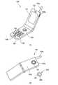
図1は、本発明の一実施形態が適用された携帯電話の外観斜視図である。この携帯電話100には、被写体を撮影する撮影機能が搭載されており、背面に設けられた撮影レンズ100上に交換レンズが着脱自在に装着される。 FIG. 1 is an external perspective view of a mobile phone to which an embodiment of the present invention is applied. This
図1のパート(A)には、携帯電話100の前面図が示されている。携帯電話100の前面には、メニュー画面や、撮影画像などが表示される液晶パネル101、内部にスピーカ(図2参照)が配備され、スピーカから発せられる音声を放つための送話口102、電話局を介して音声やメールなどのデータを送受信するための第1アンテナ103a、各種機能の選択や、撮影を行う際のシャッタボタンとして使用される選択ボタン104、電話番号を入力するためのプッシュボタン105、内部にマイクロフォン(図2参照)が配備され、声をマイクロフォンに伝えるための受話口106、ユーザが入力した電話番号などを確定する確定ボタン107、電源ボタン108、および電話局を介さずに、近距離用の無線通信によって画像やアドレス情報などを送受信するための第2アンテナ109aが備えられている。 Part (A) of FIG. 1 shows a front view of the
図1のパート(B)には、携帯電話100の背面図が示されている。携帯電話100の背面には、撮影レンズ110が設けられており、携帯電話100の筐体100aには、撮影レンズ110を取り囲むドーナツ状の磁石110aが取り付けられている。また、携帯電話100には、撮影レンズ110上に取り付けられる、ズームレンズや魚眼レンズなどといった各種の交換レンズ200が用意されている。交換レンズ200は、透明なレンズ部分201上に透明な磁性膜202が形成されたものである(磁性膜202を構成する物質、および交換レンズ200の製造方法については後述する)。この磁性膜202が撮影レンズ110に取り付けられた磁石110aに磁力で引き付けられることによって、交換レンズ200が携帯電話100に装着される。このレンズ部分201は、本発明にいう基体の一例にあたり、磁性膜202は、本発明にいう磁性膜の一例に相当する。また、筐体100aは、本発明にいう筐体の一例にあたり、磁石110aは、本発明にいうマウント部の一例に相当する。 Part (B) of FIG. 1 shows a rear view of the
図2は、交換レンズ200が装着された携帯電話100の側面図である。 FIG. 2 is a side view of the
交換レンズ200は、図1のパート(B)に示す磁性膜202が携帯電話100の磁石110aに引き付けられている。交換レンズ200の光透過面上に透明な磁性膜202を設けることによって、交換レンズ200を取り囲む部品などを取り付ける必要がなく、交換レンズ200を小型化することができる。 In the
ここで、携帯電話100の内部構造について説明する。 Here, the internal structure of the
図3は、携帯電話100の内部ブロック図である。 FIG. 3 is an internal block diagram of the
携帯電話100の内部には、撮影レンズ110、アイリス111、CCD112、A/D(Analog/Degital)変換部113、マイクロフォン121、スピーカ122、インタフェース部120、第1送受信部103、入力コントローラ130、画像信号処理部140、ビデオエンコーダ150、画像表示装置160、第2送受信部109、メモリ170、CPU180、メディアコントローラ190、各種スイッチ181が具備されており、さらに、記録メディア300が接続されている。 In the
各種スイッチ181には、図1に示す選択ボタン104やプッシュボタン105などが含まれる。これら各種スイッチ181が押下されると、そのスイッチが入ったことがCPU180に伝えられる。 The various switches 181 include the
CPU180は、図3に示す携帯電話100の各種要素に処理の指示を伝えて、各種要素を制御する。例えば、撮影を行う撮影モードが設定された状態で図1の選択ボタン104が押下されると、CPU180から図3に示す各種要素に指示が与えられ、撮影が開始される。 The
本来、被写体を撮影する撮影装置には複数のレンズが配備されるが、この図3では、それら複数のレンズを撮影レンズ110として模式的に示している。また、アイリス111は、CCD112で受光される被写体光の光量を調整する絞りである。 Originally, a plurality of lenses are provided in a photographing apparatus that photographs a subject. In FIG. 3, these lenses are schematically illustrated as photographing
撮影が開始されると、CCD112は、撮影レンズ110を通ってきた被写体光を受光して、被写体光に基づく被写体像をアナログ信号である被写体信号として読み取る。このCCD112は、本発明にいう撮像部の一例に相当する。CCD112で生成された被写体信号は、A/D変換部115でデジタルの撮影画像データに変換される。変換後の撮影画像データは、入力コントローラ130を介して画像信号処理部140に送られる。 When photographing is started, the
画像信号処理部140では、画像データにRGBレベルの調節、ガンマ調整等といった画像処理が施され、さらに、画像処理後の画像データに圧縮処理が施される。圧縮後の画像データは、一旦メモリ170に送られる。 The image
メモリ170には、この携帯電話100内で実行されるプログラムが記憶されたり、中間バッファとして用いられる記録速度が高速なSDRAM、各種メニュー画面用のデータや、ユーザの設定内容などが記憶されたデータ保存用のメモリであるSRAM、圧縮された画像データが記憶されるVRAMが含まれている。VRAMは、複数領域に分割されており、画像データが複数領域に順番に記憶され、記憶された画像データはビデオエンコーダ150やメディアコントローラ190に順次に読み出される。 The
ビデオエンコーダ150は、CPU180からの指示に従って、メモリ170から圧縮後の画像データを取得し、圧縮後の画像データを、液晶パネル101で表示できるデータ形式に変換する。変換後の画像データは画像表示装置130に送られ、画像表示装置130によって、画像データが表す画像が液晶パネル101に表示される。メディアコントローラ190は、メモリ170に記憶された圧縮後の画像データを記録メディア300へ記録したり、記録メディア300に記録された画像データを読み出すためのものである。 The
また、図1に示すプッシュボタン105を使って電話番号が入力され、確定ボタン107が押下されると、電話番号が設定されて相手装置との通信が開始される。このとき、携帯電話100の電話番号や入力された電話番号などの通信情報がCPU180から第1送受信部103に伝えられ、通信情報が電波に変換されてアンテナ103aに伝えられ、アンテナ103aから電波が発せられる。第1アンテナ103aから発せられた電波は、建物や電柱などといった各所に設けられている共同アンテナ(図示しない)を介して電話局に伝わり、電話局で、指定された電話番号が割り当てられた相手装置との接続が確立される。 Further, when a telephone number is input using the
相手装置との接続が確立すると、ユーザが携帯電話100に向けて発した声が、図1にも示すマイクロフォン106で集音され、集音された声がインタフェース部120で音声データを表わす電波に変換されて、第1送受信部103の第1アンテナ103aによって相手装置に送信される。また、第1アンテナ103aを介して受信された音声用の電波は、インタフェース部120で音声データに変換され、図1にも示すスピーカ102から音声として発せられる。第1送受信部103、第1アンテナ103aでは、音声データだけではなく、電話番号の代わりにメールアドレスを使ってメールを表わすメールデータも送受信される。第1アンテナ103aで受信されて、第1送受信部103でデジタル化されたメールデータは、入力コントローラ130によってメモリ170に記憶される。 When the connection with the counterpart device is established, the voice uttered by the user toward the
また、この携帯電話100には、電話局を介して他の携帯電話などといった相手装置と通信するための通信インタフェース(第1送受信部103、第1アンテナ103a)とは別に、電話局を介さずに、近距離用の無線通信によって通信するための無線通信インタフェース(第2送受信部109、第2アンテナ109a)も備えられている。近距離無線通信用の通信インタフェースとしては、赤外線通信やブルートゥース(Bluetooth)などを適用することができる。本実施形態では、通信インタフェースとして赤外線通信が適用されており、他の携帯電話などから直接送信されてきた赤外線が第2アンテナ109aで受信されると、その受信された赤外線に基づく電気信号が第2送受信部109でピックアップされて、デジタルのデータに変換される。逆に、外部装置にデータを送信するときには、第2送受信部109にデータが伝えられ、そのデータが第2送受信部109で電波に変換されて、第2アンテナ109aから発せられる。 In addition, the
この第2アンテナ109aで画像を表わす赤外線が受信されると、第2送受信部109では赤外線に基づく電気信号が画像データに変換される。変換された画像データは、撮影画像データと同様にして、画像表示装置160に送られて画像データが表わす画像が液晶パネル101に表示されたり、メディアコントローラ190を介して記録メディア300に記録される。 When infrared rays representing an image are received by the
携帯電話100は、基本的には以上のように構成されている。 The
ここで、携帯電話100は小型であるため、ズームレンズなどを内蔵することが困難であるが、小型の交換レンズ200を装着することによって、接写撮影を実現することができる。このとき、図2に示すように、交換レンズ200および撮影レンズ110を通過してきた被写体光がCCD112で受光され、被写体光に基づいた撮影画像データが生成される。このように、本実施系形態の携帯電話100によると、所望の光学条件に適した交換レンズ200を装着して、様々な撮影画像を取得することができる。 Here, since the
続いて、交換レンズ200の製造方法について説明する。 Next, a method for manufacturing the
図4は、交換レンズ200の製造方法を説明する図である。 FIG. 4 is a diagram illustrating a method for manufacturing the
まず、透明物質(例えば、ガラスやプラスチックなど)をレンズ形状に成型して、図1のパート(B)にも示すレンズ部分201を形成する(図4のステップS11)。このレンズ部分201を形成するステップS11の過程は、本発明の第1の光学素子製造方法における基体形成過程の一例に相当する。 First, a transparent material (for example, glass or plastic) is molded into a lens shape to form a
続いて、レンズ部分201上に形成される磁性膜202の元となるターゲットを作成する(図4のステップS12)。本実施形態では、ルチル結晶構造の二酸化チタンにコバルトを10mol%ドープして1000度で焼結することにより、二酸化チタン・コバルトで構成されたターゲット411を作成した。この二酸化チタン・コバルトは、透明な磁性体である。 Subsequently, a target serving as a base of the
ターゲット411が作成されると、そのターゲット411を構成する磁性体(二酸化チタン・コバルト)を、レーザアブレーションによって、ステップS11で形成されたレンズ部分201上に積層させる(図4のステップS13)。このステップS13では、まず、レンズ部分201上の、磁性膜を形成しない部分をマスクする。続いて、レンズ部分201を加熱するとともに、ターゲット411にレーザ光を照射して表面を瞬間的に気化させることで二酸化チタン・コバルトの微小粒子412を発生させ、その二酸化チタン・コバルトの微小粒子412をレンズ部分201上に積層させる。このレンズ部分201を加熱する加熱装置としては、Nd:YAGレーザを使用した基板加熱装置などを使用することができ、ターゲット411にレーザを照射する照射装置としては、248nmのレーザ光を出射するKrFエキシマレーザなどを使用することができる。レンズ部分201上に微小粒子412を積層させるステップS13の過程は、本発明の第1の光学素子製造方法における膜形成過程の一例に相当する。 When the
尚、二酸化チタン・コバルトのターゲットと、ルチル結晶構造の二酸化チタンのみからなるターゲットとの2つのターゲットを使用し、これらのターゲットを所定数比率のレーザ光を交互に照射して磁性膜を形成しても良い。 Two targets, a target of titanium dioxide / cobalt and a target made of only titanium dioxide having a rutile crystal structure, are used, and a magnetic film is formed by alternately irradiating these targets with a predetermined number of laser beams. May be.
ここで、本発明においては、この交換レンズ200を透明磁石として用いてもよい。この場合、ステップS13において、上述した処理に加えて以下に示すような処理を実行して、交換レンズ200の磁性膜202を磁化する。 Here, in the present invention, the
磁性膜202が磁化されていない状態とは、磁性膜202を構成している各微小粒子412のN極とS極が揃っていない状態である。磁性膜202を磁化するには、微小粒子412を積層する際に、レンズ部分201の裏面に大きな磁極を印加しておく。例えば、レンズ部分201に磁石600のN極を近づけておくと、微小粒子412のS極が磁石600のN極に引き付けられ、微小粒子412が、S極側がレンズ部分201と接触するように磁極を揃えて積層される。その結果、N極側が表面に露出した磁性膜202が形成され、表面がN極の透明磁石である交換レンズ200が作成される。 The state in which the
また、磁性体の磁化方法については、この他にも様々に知られており、それらの方法を適用することもできる。 In addition to this, there are various known methods for magnetizing the magnetic material, and these methods can also be applied.
レンズ部分201上に二酸化チタン・コバルトが積層されたら、マスクを除去する(図4のステップS14)。このようにして、透明なレンズ部分201上に透明な二酸化チタン・コバルトの磁性膜202が形成された交換レンズ200を生成する。このようにして得られた二酸化チタン・コバルト磁性膜202の膜厚は、200nmであった。 When the titanium dioxide / cobalt is laminated on the
また、本実施形態においては、交換レンズ200に対して光透過性を向上させるためや、図1のパート(B)に示すリング状の磁石110aの正しい位置に装着されるように、レンズ部分201の周辺部分のみにリング状に磁性膜202を形成する例について説明したが、本発明においては、レンズ部分201上の面全体に磁性膜を形成してもよい。 Further, in the present embodiment, the
以上で、本発明の第1実施形態の説明を終了し、本発明の第2実施形態について説明する。第1実施形態と第2実施形態とではほぼ同じ構成を有するため、以下では、第1実施形態との共通要素については同じ符号を付して説明を省略し、第1実施形態との相違点のみ説明する。 Above, description of 1st Embodiment of this invention is complete | finished and 2nd Embodiment of this invention is described. Since the first embodiment and the second embodiment have substantially the same configuration, in the following, common elements with the first embodiment are denoted by the same reference numerals, description thereof is omitted, and differences from the first embodiment are omitted. Only explained.
図5は、本発明の第2実施形態の携帯電話の背面図である。 FIG. 5 is a rear view of the mobile phone according to the second embodiment of the present invention.
本実施形態の携帯電話100´は、図1のパート(B)に示す第1実施形態の携帯電話100とほぼ同様の内部構造を有するが、携帯電話100´には、磁石110aに替えて磁性体110bが取り付けられている。また、この携帯電話100´には、透明な磁石で構成された平行平面板200´が取り付けられる。この平行平面板200´は、透明な媒体中に透明な磁性粒203が混合され、その磁性粒203が磁化されて形成されたものである(平行平面板200´を構成する物質、および製造方法については後述する)。磁性粒203は、本発明にいう磁性材料の粒の一例に相当する。携帯電話100´では、筐体100aに取り付けられた磁性体110bと、透明磁石で構成された平行平面板200´とが磁力で引き付けあい、平行平面板200´が携帯電話100´に装着される。このように、携帯電話にレンズではなく平行平面板を装着してもよく、また、携帯電話の筐体に磁性体を取り付けて、透明磁石で構成された平行平面板やレンズを装着してもよい。 The
続いて、平行平面板200´の製造方法について説明する。 Then, the manufacturing method of parallel plane plate 200 'is demonstrated.
図4は、平行平面板200´の製造方法を説明する図である。 FIG. 4 is a diagram for explaining a method of manufacturing the plane-
まず、チタンテトラアルコキサイドにコバルトを加えた磁性材料511を真空下で加熱する(図6のステップS1)。その結果、磁性材料511が脱アルコール処理されて、二酸化チタンとコバルトがドープされた磁性粒203が形成される(図6のステップS22)。さらに、磁性粒203に安定化剤(チタンカップリング剤:イソプロピルトリイソステアロイルチタネートなど)を添加して、磁性粒203を安定して分散させる。本実施形態においては、ルチル結晶構造の二酸化チタンにコバルトが10mol%ドープされた磁性粒203を生成したところ、磁性粒203の平均粒径は10nmであった。このステップS21およびステップS22における磁性粒を生成する過程は、本発明の第2の光学素子製造方法における粒化過程の一例に相当する。 First, a
続いて、透明な流動媒体512に、磁性粒203を混合する(図6のステップS23)。本実施形態では、流動媒体512としてポリメチルメタクリレートが用いられ、この流動媒体512中に二酸化チタン・コバルトの磁性粒203が10mol%程度混合される。このステップS22における流動媒体に磁性粒を混合する過程は、本発明の第2の光学素子製造方法における混合過程の一例に相当する。 Subsequently, the
さらに、磁性粒203が混合された流動媒体512を平行平面板形状に射出成型して固化する(図6のステップS24)。その結果、磁性粒203が混合された平行平面板200´が生成される。このステップS24の流動媒体を固化する過程は、本発明の第2の光学素子製造方法における成型過程の一例に相当する。 Furthermore, the fluidized medium 512 mixed with the
尚、ステップS24の固化過程で、上述したステップS13と同様にして流動媒体512に磁石600の磁極を印加すると、磁性粒203の磁極が揃った状態で固化されて、平行平面板200´が磁化される(図6のステップS25)。 In the solidification process in step S24, when the magnetic poles of the
以上のようにして、透明磁石である平行平面板200´が作成される。 As described above, the plane
ここで、上記では、本発明にいう撮像装置の一例として携帯電話が示されているが、本発明にいう撮像装置はデジタルカメラなどであってもよい。 Here, in the above, a mobile phone is shown as an example of the imaging apparatus according to the present invention, but the imaging apparatus according to the present invention may be a digital camera or the like.
また、上記では、本発明にいう撮像部の一例としてCCDが示されているが、本発明にいう撮像部はCMOSセンサなどであってもよい。 In the above description, the CCD is shown as an example of the imaging unit according to the present invention. However, the imaging unit according to the present invention may be a CMOS sensor or the like.
また、上記では、本発明にいうマウント部の一例として不透明な磁石や磁性体が示されているが、本発明にいうマウント部も透明な磁石や磁性体で構成されたものであってもよい。上記では、大きな磁力を得るために、通常の不透明な磁石などを使用した。 In the above description, an opaque magnet or magnetic material is shown as an example of the mount portion according to the present invention. However, the mount portion according to the present invention may also be composed of a transparent magnet or magnetic material. . In the above, a normal opaque magnet or the like is used in order to obtain a large magnetic force.
100 携帯電話
100a 筐体
101 液晶パネル
102 送話口
103 第1送受信部
103a 第1アンテナ
104 選択ボタン
105 プッシュボタン
106 受話口
107 確定ボタン
108 電源ボタン
109 第2送受信部
109a 第2アンテナ
110 撮影レンズ
110a 磁石
111 アイリス
112 CCD
113 A/D変換部
120 インタフェース部
121 マイクロフォン
122 スピーカ
130 入力コントローラ
140 画像信号処理部
150 ビデオエンコーダ
160 画像表示装置
170 メモリ
180 CPU
181 各種スイッチ
190 メディアコントローラ
200 交換レンズ
201 レンズ部分
202 磁性膜
300 記録メディア
DESCRIPTION OF
113 A /
181 Various switches 190
Claims (9)
Translated fromJapanese前記基体の透明な面上に設けられた、光透過性を有する磁性膜とを備えたことを特徴とする光学素子。A substrate that transmits light at least in a predetermined optical axis direction;
An optical element comprising: a light-transmitting magnetic film provided on a transparent surface of the substrate.
前記基体中に散在した、光透過性を有する磁性粒とを備えたことを特徴とする光学素子。A substrate that transmits light at least in a predetermined optical axis direction;
An optical element comprising: light-transmitting magnetic particles scattered in the substrate.
光透過性の磁性材料を、前記基体形成過程で形成された基体上に複数層積層させて所定の厚さの磁性膜を形成する膜形成過程とを有することを特徴とする光学素子製造方法。A substrate forming process of forming a substrate of a predetermined shape with a light transmissive material;
An optical element manufacturing method comprising: forming a magnetic film having a predetermined thickness by laminating a plurality of light transmissive magnetic materials on a base formed in the base forming process.
前記粒化過程で得られた磁性材料の粒を、光透過性を有する流動媒体中に混合する混合過程と、
前記混合過程で前記磁性材料が混合された流動媒体を固化して成型する成型過程とを有することを特徴とする光学素子製造方法。A granulation process for granulating a light-transmitting magnetic material;
A mixing process in which the particles of the magnetic material obtained in the granulating process are mixed in a fluid medium having optical transparency;
A method for producing an optical element, comprising: solidifying and molding a fluid medium mixed with the magnetic material in the mixing process.
筐体と、
前記筐体上に設けられた、磁性を有し、前記光学素子が磁力によって着脱自在に装着されるマウント部と、
前記筐体内に設けられた、前記マウント部に装着された光学素子を通ってきた被写体光に基づいて撮影画像を取得する撮像部とを備えたことを特徴とする撮像装置。An optical element having magnetism that transmits light at least in a predetermined optical axis direction;
A housing,
A mount portion provided on the housing, having magnetism, to which the optical element is detachably mounted by a magnetic force;
An imaging apparatus comprising: an imaging unit provided in the housing that acquires a captured image based on subject light that has passed through an optical element attached to the mount unit.
Priority Applications (1)
| Application Number | Priority Date | Filing Date | Title |
|---|---|---|---|
| JP2005065390AJP2006251150A (en) | 2005-03-09 | 2005-03-09 | Optical element, method for manufacturing optical element, and imaging apparatus |
Applications Claiming Priority (1)
| Application Number | Priority Date | Filing Date | Title |
|---|---|---|---|
| JP2005065390AJP2006251150A (en) | 2005-03-09 | 2005-03-09 | Optical element, method for manufacturing optical element, and imaging apparatus |
Publications (1)
| Publication Number | Publication Date |
|---|---|
| JP2006251150Atrue JP2006251150A (en) | 2006-09-21 |
Family
ID=37091758
Family Applications (1)
| Application Number | Title | Priority Date | Filing Date |
|---|---|---|---|
| JP2005065390AWithdrawnJP2006251150A (en) | 2005-03-09 | 2005-03-09 | Optical element, method for manufacturing optical element, and imaging apparatus |
Country Status (1)
| Country | Link |
|---|---|
| JP (1) | JP2006251150A (en) |
Cited By (20)
| Publication number | Priority date | Publication date | Assignee | Title |
|---|---|---|---|---|
| ITVR20110063A1 (en)* | 2011-03-30 | 2012-10-01 | Maurizio Marcato | OPTICAL ACCESSORY FOR SMARTPHONE, PDA AND / OR PALMARI OR SIMILAR |
| US8279544B1 (en) | 2011-03-18 | 2012-10-02 | Premier Systems USA, Inc | Selectively attachable and removable lenses for communication devices |
| USD678379S1 (en) | 2011-12-30 | 2013-03-19 | Premier Systems Usa, Inc. | Lens component |
| USD697958S1 (en) | 2012-10-30 | 2014-01-21 | Premier Systems Usa, Inc. | Lens component |
| JP2014025879A (en)* | 2012-07-30 | 2014-02-06 | Konica Minolta Inc | Sensor chip and optical device for detecting specimen having the sensor chip |
| USD726796S1 (en) | 2013-11-21 | 2015-04-14 | Olloclip, Llc | Optical component |
| US9007522B1 (en) | 2013-09-26 | 2015-04-14 | Olloclip, Llc | Selectively attachable and removable optical systems for mobile devices |
| USD727385S1 (en) | 2013-11-21 | 2015-04-21 | Olloclip, Llc | Optical component |
| USD727868S1 (en) | 2013-11-21 | 2015-04-28 | Olloclip, Llc | Optical component |
| US9195023B2 (en) | 2012-09-12 | 2015-11-24 | Olloclip, Llc | Removable optical devices for mobile electronic devices |
| JP2016505172A (en)* | 2013-02-05 | 2016-02-18 | リム,ソン−キュ | Auxiliary lens removable glasses |
| US9294660B2 (en) | 2013-03-13 | 2016-03-22 | Olloclip, Llc | Removable lenses for mobile electronic devices |
| USD754228S1 (en) | 2014-02-19 | 2016-04-19 | olioclip, LLC | Optical component |
| USD761896S1 (en) | 2014-04-11 | 2016-07-19 | Olloclip, Llc | Optical component |
| USD763340S1 (en) | 2014-10-02 | 2016-08-09 | Olloclip, Llc | Optical component |
| US9454066B2 (en) | 2014-06-19 | 2016-09-27 | Olloclip, Llc | Auxiliary optical components for mobile devices |
| US9544539B2 (en) | 2009-06-29 | 2017-01-10 | Kendyl A Roman | Optical adapters for mobile devices with a camera |
| US9661200B2 (en) | 2013-08-07 | 2017-05-23 | Olloclip, Llc | Auxiliary optical components for mobile devices |
| US10088738B2 (en) | 2014-04-11 | 2018-10-02 | Portero Holdings, Llc | Auxiliary optical devices |
| JP2018185538A (en)* | 2014-08-07 | 2018-11-22 | ハウンディニックス エルエルシー | Low-profile lens mount |
- 2005
- 2005-03-09JPJP2005065390Apatent/JP2006251150A/ennot_activeWithdrawn
Cited By (32)
| Publication number | Priority date | Publication date | Assignee | Title |
|---|---|---|---|---|
| US9544539B2 (en) | 2009-06-29 | 2017-01-10 | Kendyl A Roman | Optical adapters for mobile devices with a camera |
| US9651756B2 (en) | 2011-03-18 | 2017-05-16 | Olloclip, Llc | Lenses for communication devices |
| US9188764B2 (en) | 2011-03-18 | 2015-11-17 | Olloclip, Llc | Lenses for communication devices |
| US8593745B2 (en) | 2011-03-18 | 2013-11-26 | Premier Systems Usa, Inc. | Lenses for communication devices |
| US10203474B2 (en) | 2011-03-18 | 2019-02-12 | Portero Holdings, Llc | Method of attaching an auxiliary lens to a mobile telephone |
| US8891187B2 (en) | 2011-03-18 | 2014-11-18 | Olloclip, Llc | Lenses for communication devices |
| US8279544B1 (en) | 2011-03-18 | 2012-10-02 | Premier Systems USA, Inc | Selectively attachable and removable lenses for communication devices |
| US9335509B2 (en) | 2011-03-18 | 2016-05-10 | Olloclip, Llc | Lenses for communication devices |
| ITVR20110063A1 (en)* | 2011-03-30 | 2012-10-01 | Maurizio Marcato | OPTICAL ACCESSORY FOR SMARTPHONE, PDA AND / OR PALMARI OR SIMILAR |
| USD686265S1 (en) | 2011-12-30 | 2013-07-16 | Premier Systems Usa, Inc. | Lens component |
| USD700228S1 (en) | 2011-12-30 | 2014-02-25 | Premier Systems Usa, Inc. | Optical component mount |
| USD678379S1 (en) | 2011-12-30 | 2013-03-19 | Premier Systems Usa, Inc. | Lens component |
| JP2014025879A (en)* | 2012-07-30 | 2014-02-06 | Konica Minolta Inc | Sensor chip and optical device for detecting specimen having the sensor chip |
| US9195023B2 (en) | 2012-09-12 | 2015-11-24 | Olloclip, Llc | Removable optical devices for mobile electronic devices |
| USD723601S1 (en) | 2012-10-30 | 2015-03-03 | Olloclip, Llc | Optical component mount |
| USD697958S1 (en) | 2012-10-30 | 2014-01-21 | Premier Systems Usa, Inc. | Lens component |
| JP2016505172A (en)* | 2013-02-05 | 2016-02-18 | リム,ソン−キュ | Auxiliary lens removable glasses |
| US9294660B2 (en) | 2013-03-13 | 2016-03-22 | Olloclip, Llc | Removable lenses for mobile electronic devices |
| US9661200B2 (en) | 2013-08-07 | 2017-05-23 | Olloclip, Llc | Auxiliary optical components for mobile devices |
| US10447905B2 (en) | 2013-08-07 | 2019-10-15 | Portero Holdings, Llc | Auxiliary optical device having moveable portions |
| US9007522B1 (en) | 2013-09-26 | 2015-04-14 | Olloclip, Llc | Selectively attachable and removable optical systems for mobile devices |
| USD727868S1 (en) | 2013-11-21 | 2015-04-28 | Olloclip, Llc | Optical component |
| USD726796S1 (en) | 2013-11-21 | 2015-04-14 | Olloclip, Llc | Optical component |
| USD727385S1 (en) | 2013-11-21 | 2015-04-21 | Olloclip, Llc | Optical component |
| USD754228S1 (en) | 2014-02-19 | 2016-04-19 | olioclip, LLC | Optical component |
| USD761896S1 (en) | 2014-04-11 | 2016-07-19 | Olloclip, Llc | Optical component |
| US10088738B2 (en) | 2014-04-11 | 2018-10-02 | Portero Holdings, Llc | Auxiliary optical devices |
| US10437137B2 (en) | 2014-04-11 | 2019-10-08 | Portero Holdings, Llc | Removable lenses for mobile devices with on-board camera |
| US9454066B2 (en) | 2014-06-19 | 2016-09-27 | Olloclip, Llc | Auxiliary optical components for mobile devices |
| US10488742B2 (en) | 2014-06-19 | 2019-11-26 | Portero Holdings, Llc | Multi-lens optical attachment for mobile devices |
| JP2018185538A (en)* | 2014-08-07 | 2018-11-22 | ハウンディニックス エルエルシー | Low-profile lens mount |
| USD763340S1 (en) | 2014-10-02 | 2016-08-09 | Olloclip, Llc | Optical component |
Similar Documents
| Publication | Publication Date | Title |
|---|---|---|
| JP2006251150A (en) | Optical element, method for manufacturing optical element, and imaging apparatus | |
| CN102783136B (en) | For taking the imaging device of self-portrait images | |
| JP4654015B2 (en) | Camera device | |
| US9055220B1 (en) | Enabling the integration of a three hundred and sixty degree panoramic camera within a mobile device case | |
| WO2015052960A1 (en) | Imaging device, imaging system, imaging method and imaging program | |
| JP2008107784A (en) | Image blurring correction unit, image blurring correction device, photographing apparatus and portable apparatus | |
| JP2009071495A (en) | Mobile terminal | |
| JP2008033029A (en) | Optical unit and photographing apparatus | |
| JP2005006271A (en) | Image capturing apparatus | |
| JP4257508B2 (en) | Electronic camera | |
| CN112468686B (en) | Camera module and mobile terminal having the same | |
| JP2008312040A (en) | Photographing unit, photographing device, portable equipment, and method for assembling photographing unit | |
| JP2001230954A (en) | Image pickup device | |
| JP2009020476A (en) | Image blurring correction unit, image blurring correction apparatus, photographing apparatus and portable device | |
| JP2009058805A (en) | Image blur correcting unit, image blur correcting device, photographing apparatus and portable device | |
| JP2008026634A (en) | Driving unit, driving device, hand blurring correction unit and photographing device | |
| JP2004096656A (en) | Mobile terminal with camera, lens selection method to be used therefor and program thereof | |
| JP2005039400A (en) | Electronic apparatus | |
| JP2006251151A (en) | Lens drive and imaging apparatus | |
| JP2008244735A (en) | camera | |
| JP2004158930A (en) | Mobile electronic apparatus incorporating camera | |
| KR20190015452A (en) | Digital photographing system and method for operating digital photographing system | |
| CN101349855B (en) | Image shake correction unit and device thereof, photography device and mobile device | |
| JP2008310168A (en) | Photographing unit, photographing device and portable apparatus | |
| JP2003234932A (en) | Roll film shaped image pickup device |
Legal Events
| Date | Code | Title | Description |
|---|---|---|---|
| A711 | Notification of change in applicant | Free format text:JAPANESE INTERMEDIATE CODE: A712 Effective date:20061214 | |
| A300 | Withdrawal of application because of no request for examination | Free format text:JAPANESE INTERMEDIATE CODE: A300 Effective date:20080513 |