JP2006250984A - Electrooptical apparatus, manufacturing method for the same and electronic equipment - Google Patents
Electrooptical apparatus, manufacturing method for the same and electronic equipmentDownload PDFInfo
- Publication number
- JP2006250984A JP2006250984AJP2005063423AJP2005063423AJP2006250984AJP 2006250984 AJP2006250984 AJP 2006250984AJP 2005063423 AJP2005063423 AJP 2005063423AJP 2005063423 AJP2005063423 AJP 2005063423AJP 2006250984 AJP2006250984 AJP 2006250984A
- Authority
- JP
- Japan
- Prior art keywords
- substrate
- pixel
- conduction
- driving circuit
- electrically connected
- Prior art date
- Legal status (The legal status is an assumption and is not a legal conclusion. Google has not performed a legal analysis and makes no representation as to the accuracy of the status listed.)
- Pending
Links
- 238000004519manufacturing processMethods0.000titleclaimsdescription46
- 239000000758substrateSubstances0.000claimsabstractdescription232
- 238000000034methodMethods0.000claimsabstractdescription56
- 239000004065semiconductorSubstances0.000claimsabstractdescription13
- 239000004020conductorSubstances0.000claimsabstractdescription11
- 239000000463materialSubstances0.000claimsdescription28
- 239000010409thin filmSubstances0.000claimsdescription5
- 239000004973liquid crystal related substanceSubstances0.000abstractdescription62
- 239000013078crystalSubstances0.000abstract1
- 230000015572biosynthetic processEffects0.000description41
- 239000010408filmSubstances0.000description31
- 229910021420polycrystalline siliconInorganic materials0.000description22
- 229920005591polysiliconPolymers0.000description22
- 238000010586diagramMethods0.000description16
- 239000011521glassSubstances0.000description16
- 239000010410layerSubstances0.000description15
- 229910021417amorphous siliconInorganic materials0.000description12
- 239000012535impuritySubstances0.000description12
- 238000001994activationMethods0.000description11
- 239000003566sealing materialSubstances0.000description11
- 239000011159matrix materialSubstances0.000description9
- 230000004913activationEffects0.000description8
- 239000002245particleSubstances0.000description8
- 238000000206photolithographyMethods0.000description8
- 230000005611electricityEffects0.000description5
- 238000005516engineering processMethods0.000description5
- 230000003068static effectEffects0.000description4
- 239000000470constituentSubstances0.000description3
- 230000010354integrationEffects0.000description3
- XUIMIQQOPSSXEZ-UHFFFAOYSA-NSiliconChemical compound[Si]XUIMIQQOPSSXEZ-UHFFFAOYSA-N0.000description2
- 230000007547defectEffects0.000description2
- 238000006356dehydrogenation reactionMethods0.000description2
- 230000005684electric fieldEffects0.000description2
- 230000001678irradiating effectEffects0.000description2
- 239000002184metalSubstances0.000description2
- 230000004048modificationEffects0.000description2
- 238000012986modificationMethods0.000description2
- 230000002093peripheral effectEffects0.000description2
- 238000005070samplingMethods0.000description2
- 239000000565sealantSubstances0.000description2
- 229910052710siliconInorganic materials0.000description2
- 239000010703siliconSubstances0.000description2
- 238000002834transmittanceMethods0.000description2
- 230000003213activating effectEffects0.000description1
- 238000000137annealingMethods0.000description1
- 239000003990capacitorSubstances0.000description1
- 230000001413cellular effectEffects0.000description1
- 238000005520cutting processMethods0.000description1
- 230000000694effectsEffects0.000description1
- 238000005401electroluminescenceMethods0.000description1
- 238000005247getteringMethods0.000description1
- 238000010438heat treatmentMethods0.000description1
- 239000011229interlayerSubstances0.000description1
- 239000002923metal particleSubstances0.000description1
- 230000003287optical effectEffects0.000description1
- 238000013386optimize processMethods0.000description1
- 230000005693optoelectronicsEffects0.000description1
- 238000007639printingMethods0.000description1
- 239000011347resinSubstances0.000description1
- 229920005989resinPolymers0.000description1
- 239000007790solid phaseSubstances0.000description1
- 239000000126substanceSubstances0.000description1
- 230000001360synchronised effectEffects0.000description1
Images


Classifications
- G—PHYSICS
- G02—OPTICS
- G02F—OPTICAL DEVICES OR ARRANGEMENTS FOR THE CONTROL OF LIGHT BY MODIFICATION OF THE OPTICAL PROPERTIES OF THE MEDIA OF THE ELEMENTS INVOLVED THEREIN; NON-LINEAR OPTICS; FREQUENCY-CHANGING OF LIGHT; OPTICAL LOGIC ELEMENTS; OPTICAL ANALOGUE/DIGITAL CONVERTERS
- G02F1/00—Devices or arrangements for the control of the intensity, colour, phase, polarisation or direction of light arriving from an independent light source, e.g. switching, gating or modulating; Non-linear optics
- G02F1/01—Devices or arrangements for the control of the intensity, colour, phase, polarisation or direction of light arriving from an independent light source, e.g. switching, gating or modulating; Non-linear optics for the control of the intensity, phase, polarisation or colour
- G02F1/13—Devices or arrangements for the control of the intensity, colour, phase, polarisation or direction of light arriving from an independent light source, e.g. switching, gating or modulating; Non-linear optics for the control of the intensity, phase, polarisation or colour based on liquid crystals, e.g. single liquid crystal display cells
- G02F1/133—Constructional arrangements; Operation of liquid crystal cells; Circuit arrangements
- G02F1/136—Liquid crystal cells structurally associated with a semi-conducting layer or substrate, e.g. cells forming part of an integrated circuit
- G02F1/1362—Active matrix addressed cells
- G—PHYSICS
- G02—OPTICS
- G02F—OPTICAL DEVICES OR ARRANGEMENTS FOR THE CONTROL OF LIGHT BY MODIFICATION OF THE OPTICAL PROPERTIES OF THE MEDIA OF THE ELEMENTS INVOLVED THEREIN; NON-LINEAR OPTICS; FREQUENCY-CHANGING OF LIGHT; OPTICAL LOGIC ELEMENTS; OPTICAL ANALOGUE/DIGITAL CONVERTERS
- G02F1/00—Devices or arrangements for the control of the intensity, colour, phase, polarisation or direction of light arriving from an independent light source, e.g. switching, gating or modulating; Non-linear optics
- G02F1/01—Devices or arrangements for the control of the intensity, colour, phase, polarisation or direction of light arriving from an independent light source, e.g. switching, gating or modulating; Non-linear optics for the control of the intensity, phase, polarisation or colour
- G02F1/13—Devices or arrangements for the control of the intensity, colour, phase, polarisation or direction of light arriving from an independent light source, e.g. switching, gating or modulating; Non-linear optics for the control of the intensity, phase, polarisation or colour based on liquid crystals, e.g. single liquid crystal display cells
- G02F1/133—Constructional arrangements; Operation of liquid crystal cells; Circuit arrangements
- G02F1/1333—Constructional arrangements; Manufacturing methods
- G02F1/133351—Manufacturing of individual cells out of a plurality of cells, e.g. by dicing
- G—PHYSICS
- G02—OPTICS
- G02F—OPTICAL DEVICES OR ARRANGEMENTS FOR THE CONTROL OF LIGHT BY MODIFICATION OF THE OPTICAL PROPERTIES OF THE MEDIA OF THE ELEMENTS INVOLVED THEREIN; NON-LINEAR OPTICS; FREQUENCY-CHANGING OF LIGHT; OPTICAL LOGIC ELEMENTS; OPTICAL ANALOGUE/DIGITAL CONVERTERS
- G02F1/00—Devices or arrangements for the control of the intensity, colour, phase, polarisation or direction of light arriving from an independent light source, e.g. switching, gating or modulating; Non-linear optics
- G02F1/01—Devices or arrangements for the control of the intensity, colour, phase, polarisation or direction of light arriving from an independent light source, e.g. switching, gating or modulating; Non-linear optics for the control of the intensity, phase, polarisation or colour
- G02F1/13—Devices or arrangements for the control of the intensity, colour, phase, polarisation or direction of light arriving from an independent light source, e.g. switching, gating or modulating; Non-linear optics for the control of the intensity, phase, polarisation or colour based on liquid crystals, e.g. single liquid crystal display cells
- G02F1/133—Constructional arrangements; Operation of liquid crystal cells; Circuit arrangements
- G02F1/136—Liquid crystal cells structurally associated with a semi-conducting layer or substrate, e.g. cells forming part of an integrated circuit
- G02F1/1362—Active matrix addressed cells
- G02F1/136227—Through-hole connection of the pixel electrode to the active element through an insulation layer
Landscapes
- Physics & Mathematics (AREA)
- Nonlinear Science (AREA)
- Engineering & Computer Science (AREA)
- Microelectronics & Electronic Packaging (AREA)
- Mathematical Physics (AREA)
- Chemical & Material Sciences (AREA)
- Crystallography & Structural Chemistry (AREA)
- General Physics & Mathematics (AREA)
- Optics & Photonics (AREA)
- Liquid Crystal (AREA)
- Devices For Indicating Variable Information By Combining Individual Elements (AREA)
Abstract
Description
Translated fromJapanese本発明は、電気光学装置、その製造方法、及び電子機器に関するものである。 The present invention relates to an electro-optical device, a manufacturing method thereof, and an electronic apparatus.
近年、アクティブマトリクス型の電気光学装置を狭額縁化、低消費電力化する技術として、TFT(薄膜トランジスタ)等の画素スイッチング素子を含む画素部とともに、前記画素部に駆動信号を供給する駆動回路を同一の素子基板上に形成する技術が知られている。駆動回路を素子基板上の半導体層を用いて形成する場合、アモルファスシリコンの半導体層では駆動能力が不足するため、画素スイッチング素子と駆動回路の双方をポリシリコンの半導体層を用いて形成することが検討されている。 2. Description of the Related Art In recent years, as a technology for narrowing an active matrix electro-optical device and reducing power consumption, a pixel circuit including a pixel switching element such as a TFT (Thin Film Transistor) and a drive circuit that supplies a drive signal to the pixel unit are the same. A technique of forming on an element substrate is known. When the drive circuit is formed using the semiconductor layer on the element substrate, the drive capability is insufficient in the amorphous silicon semiconductor layer, and therefore, both the pixel switching element and the drive circuit may be formed using the polysilicon semiconductor layer. It is being considered.
例えば特許文献1には、画素部のスイッチング素子と走査線駆動回路とを同一の低温ポリシリコンプロセスで素子基板上に形成した電気光学装置が開示されている。他方、特許文献2には、素子基板とは別の駆動回路用基板に低温ポリシリコンプロセスを用いて駆動回路を形成し、前記駆動回路用基板から切り出した駆動回路片を素子基板に接着することで電気光学装置を構成する技術が開示されている。
しかし、特許文献1に記載の技術は、狭額縁化には有利であるものの、画素部と駆動回路とを同時に形成するために工程が複雑化して歩留まりが低下しやすくなるという問題がある。また特許文献2に記載の技術では、別途用意した回路片を素子基板に実装するので、従来のICチップを用いた電気光学装置と同程度のレイアウト面積が必要であるため狭額縁化にはほとんど寄与しない。さらに低温ポリシリコンプロセスを用いて形成した駆動回路片はICチップより静電気耐性が低いため取り扱いに注意を要する。 However, although the technique described in
本発明は、上記従来技術の問題点に鑑みて成されたものであって、駆動回路を内蔵しながら簡便な工程で高歩留まりに製造可能な電気光学装置とその製造方法を提供することを目的としている。 The present invention has been made in view of the above-described problems of the prior art, and an object thereof is to provide an electro-optical device that can be manufactured with a high yield in a simple process while incorporating a drive circuit. It is said.
本発明は、上記課題を解決するために、互いに対向して配置された第1基板と第2基板と具備し、前記第1基板の前記第1基板側の面に、多結晶半導体層を含む駆動回路部と、該駆動回路部に導電接続された第1導通部とが設けられ、前記第2基板の前記第1基板側の面には、画素電極と、該画素電極に導電接続された第2導通部とが設けられており、前記第1導通部と第2導通部とが、互いに平面的に重なる領域で電気的に接続されていることを特徴とする電気光学装置を提供する。
この構成によれば、当該電気光学装置の表示領域における主要部を構成する画素電極と、該画素電極に対して電気信号を供給する駆動回路部とを異なる基板に設けているので、第1基板に駆動回路部を形成する工程と、第2基板に画素電極を形成する工程とを別々の工程で行うことができる。したがって、高速動作が要求され、また高機能化のために集積度向上が要求される駆動回路部については、最小線幅の狭いフォトリソグラフィ工程を適用することができ、駆動回路部の集積度、動作速度を向上させることができる。
また、表示領域全体での均一性が要求される画素電極の形成領域については、基板上の領域で均一な加工が可能なフォトリソグラフィ工程を適用することができ、表示領域におけるスイッチング特性のばらつきを抑え、表示むらのない高品質の表示が可能になる。
さらに、駆動回路部の形成工程と画素電極の形成工程のそれぞれで最適化された工程を用いることができるため、駆動回路部及び画素電極形成領域の双方で性能及び歩留まりを向上させることができる。
また、駆動回路部と画素電極との電気的接続については、駆動回路部及び画素電極とそれぞれ電気的に接続された第1導通部と第2導通部とを、第1基板と第2基板とを貼り合わせた際に平面的に重なる位置に形成し、電気的に接続する構造としているので、第1基板と第2基板とを貼り合わせる際にこれら第1導通部と第2導通部との電気的接続も同時に成され、工数を増加させることはない。
したがって本構成によれば、高機能の駆動回路を内蔵してコンパクト化を実現しており、また高画質表示を得ることができ、さらに簡便な工程で高歩留まりに製造可能な電気光学装置が提供される。
なお、本発明において「画素電極」は、画素において電気光学物質に電圧を印加する電圧印加手段を意味し、必ずしも個々の画素ごとに区画形成された電極であることを要しない。例えば、複数の画素に跨って延在するストライプ状の電極も上記「画素電極」に含まれる。
また本明細書において、「電気光学装置」とは、電界により物質の屈折率が変化して光の透過率を変化させる電気光学効果を有するもののほか、電気エネルギーを光学エネルギーに変換する発光装置等も含んで総称したものである。In order to solve the above-described problems, the present invention includes a first substrate and a second substrate that are disposed to face each other, and includes a polycrystalline semiconductor layer on a surface of the first substrate on the first substrate side. A drive circuit unit and a first conduction unit conductively connected to the drive circuit unit are provided. A pixel electrode and a surface of the second substrate on the first substrate side are conductively connected to the pixel electrode. An electro-optical device is provided, wherein a second conduction portion is provided, and the first conduction portion and the second conduction portion are electrically connected in a region overlapping each other in a plane.
According to this configuration, since the pixel electrode constituting the main part in the display region of the electro-optical device and the drive circuit unit for supplying an electric signal to the pixel electrode are provided on different substrates, the first substrate The step of forming the drive circuit portion and the step of forming the pixel electrode on the second substrate can be performed in separate steps. Therefore, a photolithography process with a narrow minimum line width can be applied to a driver circuit portion that requires high-speed operation and that needs to be improved in integration for higher functionality. The operation speed can be improved.
In addition, for pixel electrode formation regions that require uniformity over the entire display region, a photolithography process that allows uniform processing in the region on the substrate can be applied, and variations in switching characteristics in the display region can be achieved. High quality display without any display unevenness is possible.
Furthermore, since the optimized process can be used in each of the formation process of the drive circuit portion and the formation process of the pixel electrode, the performance and the yield can be improved in both the drive circuit portion and the pixel electrode formation region.
In addition, regarding the electrical connection between the drive circuit unit and the pixel electrode, the first conduction unit and the second conduction unit that are electrically connected to the drive circuit unit and the pixel electrode, respectively, and the first substrate and the second substrate. Are formed so as to be electrically connected to each other when the first substrate and the second substrate are bonded to each other. Therefore, when the first substrate and the second substrate are bonded to each other, Electrical connections are made at the same time, and man-hours are not increased.
Therefore, according to this configuration, an electro-optical device is provided that has a built-in high-performance drive circuit to achieve a compact size, can obtain a high-quality display, and can be manufactured with a simple process and a high yield. Is done.
In the present invention, the “pixel electrode” means a voltage applying means for applying a voltage to the electro-optical material in the pixel, and does not necessarily need to be an electrode divided and formed for each pixel. For example, a stripe electrode extending across a plurality of pixels is also included in the “pixel electrode”.
In addition, in this specification, “electro-optical device” refers to a light-emitting device that converts electric energy into optical energy, in addition to an electro-optical effect that changes the light transmittance by changing the refractive index of a substance by an electric field. Is also a generic term.
本発明の電気光学装置では、前記第1導通部と第2導通部とが、前記第1基板と第2基板との間に挟持された導電部材を介して電気的に接続されている構成とすることができる。この構成によれば、第1基板と第2基板とを貼り合わせる際に上記導電部材を第1基板上又は第2基板上に配置しておくことで容易に第1導通部と第2導通部との電気的接続を形成できるので、製造容易性に優れた電気光学装置となる。 In the electro-optical device according to the aspect of the invention, the first conductive portion and the second conductive portion are electrically connected via a conductive member sandwiched between the first substrate and the second substrate. can do. According to this configuration, the first conductive portion and the second conductive portion can be easily provided by arranging the conductive member on the first substrate or the second substrate when the first substrate and the second substrate are bonded together. Thus, an electro-optical device with excellent manufacturability can be obtained.
本発明の電気光学装置では、前記第1導通部と第2導通部とを電気的に接続する導電部材が、前記第1基板と第2基板とを接合する接合材の少なくとも一部を形成していてもよい。このような構成とすれば、第1基板と第2基板とを接合する接合材が、前記第1導通部と第2導通部とを電気的に接続する機能を兼ねたものとなるので、さらに製造効率を向上させることが可能である。 In the electro-optical device according to the aspect of the invention, the conductive member that electrically connects the first conductive portion and the second conductive portion forms at least a part of a bonding material that bonds the first substrate and the second substrate. It may be. With such a configuration, the bonding material for bonding the first substrate and the second substrate also serves as a function of electrically connecting the first conductive portion and the second conductive portion. Manufacturing efficiency can be improved.
本発明の電気光学装置では、前記第1導通部及び前記第2導通部が、前記第1基板と第2基板とを接合する接合材の外側に配置されていてもよい。前記第1導通部及び第2導通部が前記接合材の内側に形成されていれば、前記両導通部の導電接続構造を前記接合材により外気から遮断でき、前記導電接続構造の電気的信頼性を高め得るものとなる。しかし、前記接合材の内側には、液晶等の電気光学物質が封止される場合があり、前記第1導通部及び第2導通部が接合材の内側に形成されていると、前記両導通部を接続するための導電部材と前記電気光学物質が接触し、電気光学物質に変質を生じる可能性もある。そこで本構成を採用することで、第1導通部と第2導通部との導電接続構造に係る構成部材と電気光学物質との接触を容易に防止することができる。 In the electro-optical device according to the aspect of the invention, the first conduction portion and the second conduction portion may be disposed outside a bonding material that joins the first substrate and the second substrate. If the first conductive portion and the second conductive portion are formed inside the bonding material, the conductive connection structure of the both conductive portions can be shielded from the outside air by the bonding material, and the electrical reliability of the conductive connection structure Can be improved. However, an electro-optical material such as liquid crystal may be sealed inside the bonding material. If the first conductive portion and the second conductive portion are formed inside the bonding material, the both conductive There is a possibility that the electro-optical material contacts with the conductive member for connecting the parts, and the electro-optical material is altered. Therefore, by adopting this configuration, it is possible to easily prevent contact between the constituent member related to the conductive connection structure between the first conductive portion and the second conductive portion and the electro-optical material.
本発明の電気光学装置では、前記第1導通部及び第2導通部に、それぞれ複数の導通端子が設けられており、前記第1導通部の導通端子と第2導通部の導通端子とが、前記第1基板と第2基板との間に設けられた異方性導電材料を介して電気的に接続されていることが好ましい。通常、駆動回路部と画素電極とは複数の接続配線を介して接続されている。そこで本構成では、前記駆動回路部から導出された複数の接続配線を前記第1導通部の複数の導通端子とそれぞれ電気的に接続し、前記画素電極から導出された複数の接続配線を前記第2導通部の複数の導通端子とそれぞれ電気的に接続するとともに、第1導通部と第2導通部との間に異方性導電材料からなる導電部材を設けた構成とすることで、第1基板と第2基板とを貼り合わせる際に、第1導通部の複数の導通端子と、それらに対応する第2導通部の各導通端子とを容易に電気的に接続できる構造となっている。これにより、効率的に駆動回路部と画素部との導電接続構造を形成することができる。 In the electro-optical device according to the aspect of the invention, each of the first conduction unit and the second conduction unit includes a plurality of conduction terminals, and the conduction terminal of the first conduction unit and the conduction terminal of the second conduction unit include It is preferable that the first substrate and the second substrate are electrically connected via an anisotropic conductive material provided. Usually, the drive circuit portion and the pixel electrode are connected via a plurality of connection wirings. Therefore, in this configuration, the plurality of connection wirings derived from the drive circuit unit are electrically connected to the plurality of conduction terminals of the first conduction unit, respectively, and the plurality of connection wirings derived from the pixel electrode are connected to the first connection unit. The first conductive portion is electrically connected to the plurality of conductive terminals of the two conductive portions, and a conductive member made of an anisotropic conductive material is provided between the first conductive portion and the second conductive portion. When the substrate and the second substrate are bonded together, the plurality of conduction terminals of the first conduction unit and the respective conduction terminals of the second conduction unit corresponding thereto can be easily electrically connected. Thereby, a conductive connection structure between the drive circuit portion and the pixel portion can be efficiently formed.
本発明の電気光学装置では、前記駆動回路部が、前記画素電極に駆動信号を供給する画素部駆動回路と、外部から入力される画像信号に信号処理を施して画素部駆動回路に出力する信号処理回路と、前記画素部駆動回路に電源を供給する電源回路とを含むことが好ましい。すなわち本発明の電気光学装置は、従来外部回路として設けられていた信号処理回路や電源回路を、画素電極に駆動信号を供給する画素部駆動回路とともに基板上に実装した構成が採用できる。このような構成とすれば、上記回路を実装した配線基板を別途電気光学装置に接続する必要が無くなり、電気光学装置のコンパクト化を実現でき、また電子機器に実装するための配線基板も小型のものを用いることができ、実装時の取り回しが容易で作業性に優れる電気光学装置となる。 In the electro-optical device according to the aspect of the invention, the driving circuit unit supplies a pixel unit driving circuit that supplies a driving signal to the pixel electrode, and a signal that performs signal processing on an externally input image signal and outputs the signal to the pixel unit driving circuit It is preferable to include a processing circuit and a power supply circuit that supplies power to the pixel portion driving circuit. That is, the electro-optical device of the present invention can employ a configuration in which a signal processing circuit and a power supply circuit, which are conventionally provided as an external circuit, are mounted on a substrate together with a pixel portion driving circuit that supplies a driving signal to a pixel electrode. With such a configuration, it is not necessary to separately connect the wiring board on which the above circuit is mounted to the electro-optical device, the electro-optical device can be made compact, and the wiring board for mounting on the electronic device is also small. The electro-optical device is easy to handle during mounting and has excellent workability.
本発明の電気光学装置では、前記画素電極が形成された領域と平面的に重なる領域の前記第1基板上にカラーフィルタが形成されている構成とすることができる。あるいは、前記画素電極が形成された領域と平面的に重なる領域の前記第2基板上に、カラーフィルタが形成されている構成であってもよい。いずれの構成においても、高画質のカラー表示が可能な電気光学装置を得ることができる。ただし、多結晶半導体層を含む駆動回路部は静電気耐性が比較的低いので、駆動回路部を含まない第2基板側にカラーフィルタを形成すれば、駆動回路部が形成された第1基板を他の工程に供することによる駆動回路部への影響を排除でき、歩留まりの向上が期待できる。 In the electro-optical device according to the aspect of the invention, a color filter may be formed on the first substrate in a region that overlaps the region in which the pixel electrode is formed in a plane. Alternatively, a color filter may be formed on the second substrate in a region that overlaps the region in which the pixel electrode is formed in a plane. In any configuration, an electro-optical device capable of high-quality color display can be obtained. However, since the drive circuit unit including the polycrystalline semiconductor layer has relatively low resistance to static electricity, if the color filter is formed on the second substrate side not including the drive circuit unit, the first substrate on which the drive circuit unit is formed is different from the first substrate. It is possible to eliminate the influence on the drive circuit portion due to the use of this process, and to improve the yield.
本発明の電気光学装置では、前記第2基板に、互いに交差して延びる複数の走査線と複数のデータ線とが形成され、前記走査線とデータ線との交差部に対応して、前記画素電極と電気的に接続された薄膜トランジスタが設けられており、前記第2導通部が、前記複数の走査線と電気的に接続された複数の走査側画素導通端子と、前記複数のデータ線と電気的に接続された複数のデータ側画素導通端子とを含んでおり、前記第1基板の駆動回路部が、前記走査線に電気信号を供給する走査線駆動回路と、前記データ線に電気信号を供給するデータ線駆動回路とを含み、前記第1導通部が、前記走査線駆動回路と電気的に接続された複数の走査側回路導通端子と、前記データ線駆動回路と電気的に接続された複数のデータ側回路導通端子とを有しており、前記走査側画素導通端子と前記走査側回路導通端子とが電気的に接続され、前記データ側画素導通端子と前記データ側回路導通端子とが電気的に接続されている構成とすることができる。 In the electro-optical device according to the aspect of the invention, a plurality of scanning lines and a plurality of data lines extending to intersect with each other are formed on the second substrate, and the pixels correspond to the intersections of the scanning lines and the data lines. A thin film transistor electrically connected to the electrode is provided, and the second conduction portion includes a plurality of scanning-side pixel conduction terminals electrically connected to the plurality of scanning lines, and the plurality of data lines and the electricity. A plurality of data-side pixel conduction terminals connected to each other, wherein the driving circuit unit of the first substrate supplies a scanning line driving circuit for supplying an electrical signal to the scanning line, and an electrical signal to the data line. A plurality of scanning-side circuit conduction terminals electrically connected to the scanning line driving circuit and the data line driving circuit. A plurality of data side circuit conduction terminals; The scanning side pixel conduction terminal and the scanning side circuit conduction terminal are electrically connected, and the data side pixel conduction terminal and the data side circuit conduction terminal are electrically connected. it can.
本発明の電気光学装置の製造方法は、第1基板の一面に、多結晶半導体層を含む駆動回路部と、該駆動回路部に導電接続された第1導通部とを形成する工程と、第2基板の一面に、画素電極と、該画素電極に導電接続された第2導通部とを形成する工程と、前記第1基板の第1導通部と前記第2基板の第2導通部とを対向させて前記第1基板と第2基板とを貼り合わせることで前記第1導通部と前記第2導通部とを電気的に接続する工程と、を有することを特徴とする。
この製造方法では、前記駆動回路部と前記画素電極とを、別々の基板に形成し、第1基板と第2基板とを貼り合わせることで前記駆動回路部と前記画素電極とを電気的に接続するようになっている。これにより、高機能化のために集積度向上が要求される駆動回路部については、最小線幅の狭いフォトリソグラフィ工程を適用して形成することができ、その結果駆動回路部の集積度、動作速度を向上させることができる。また、表示領域全体での均一性が要求される画素電極の形成領域については、基板上の領域で均一な加工が可能なフォトリソグラフィ工程を適用して形成することができるので、表示領域におけるスイッチング特性のばらつきを抑え、表示むらのない高品質の表示が可能になる。
したがって本発明に係る製造方法によれば、高機能の駆動回路部と、均一な表示特性を具備した表示領域とを備えた電気光学装置を容易かつ効率よく製造することができる。The method of manufacturing an electro-optical device according to the present invention includes forming a driving circuit unit including a polycrystalline semiconductor layer on one surface of a first substrate, and a first conductive unit electrically connected to the driving circuit unit; Forming a pixel electrode and a second conductive portion conductively connected to the pixel electrode on one surface of the two substrates; a first conductive portion of the first substrate; and a second conductive portion of the second substrate. A step of electrically connecting the first conductive portion and the second conductive portion by bonding the first substrate and the second substrate to face each other.
In this manufacturing method, the drive circuit unit and the pixel electrode are formed on separate substrates, and the drive circuit unit and the pixel electrode are electrically connected by bonding the first substrate and the second substrate together. It is supposed to be. As a result, a drive circuit portion that requires higher integration for higher functionality can be formed by applying a photolithography process with a narrow minimum line width. As a result, the integration and operation of the drive circuit portion are reduced. Speed can be improved. In addition, the pixel electrode formation region that requires uniformity over the entire display region can be formed by applying a photolithography process that allows uniform processing in the region on the substrate. Variations in characteristics are suppressed, and high-quality display without display unevenness becomes possible.
Therefore, according to the manufacturing method of the present invention, it is possible to easily and efficiently manufacture an electro-optical device including a high-performance drive circuit unit and a display region having uniform display characteristics.
本発明の電気光学装置の製造方法では、前記第1基板と第2基板との間に導電部材を介在させて前記両基板を貼り合わせることで、前記第1導通部と第2導通部とを電気的に接続することが好ましい。
この製造方法によれば、第1基板と第2基板とを貼り合わせる際に、同時に前記第1導通部と第2導通部との導電接続構造を形成することができ、電気光学装置の製造を容易かつ高効率なものとすることができる。In the method of manufacturing the electro-optical device according to the aspect of the invention, the first conductive portion and the second conductive portion are bonded to each other by attaching a conductive member between the first substrate and the second substrate. Electrical connection is preferable.
According to this manufacturing method, when the first substrate and the second substrate are bonded together, the conductive connection structure between the first conductive portion and the second conductive portion can be formed at the same time, and the electro-optical device can be manufactured. It can be easy and highly efficient.
本発明の電気光学装置の製造方法では、前記導電部材として、異方性導電材料を含むものを用いることが好ましい。この構成によれば、前記第1導通部と第2導通部のそれぞれに複数の導通端子が設けられている場合に、前記第1導通部と第2導通部との間に前記異方性導電材料を含む導電部材を配するのみで、互いに対向して配置された第1導通部の導通端子と第2導通部の導通端子とを良好に電気的に接続する一方、隣接する導通端子との短絡は良好に防止することができる。したがって本製造方法によれば、簡便な工程で信頼性に優れる導電接続構造を具備した電気光学装置を製造することができる。 In the method for manufacturing the electro-optical device according to the aspect of the invention, it is preferable that the conductive member includes an anisotropic conductive material. According to this configuration, when a plurality of conduction terminals are provided in each of the first conduction portion and the second conduction portion, the anisotropic conduction is provided between the first conduction portion and the second conduction portion. The conductive member of the first conductive part and the conductive terminal of the second conductive part, which are disposed to face each other, are electrically connected to each other only by arranging the conductive member containing the material, while the adjacent conductive terminal Short circuit can be prevented well. Therefore, according to this manufacturing method, it is possible to manufacture an electro-optical device having a conductive connection structure with excellent reliability in a simple process.
本発明の電子機器は、先に記載の本発明の電気光学装置を備えたことを特徴とする。この構成によれば、高機能の駆動回路をパネルに実装し、制御性に優れ、またコンパクトで実装性に優れた表示部を具備した電子機器を実現できる。 An electronic apparatus according to the present invention includes the electro-optical device according to the present invention described above. According to this configuration, it is possible to realize an electronic device including a display unit that is mounted with a high-performance drive circuit on a panel, is excellent in controllability, and is compact and excellent in mountability.
(液晶装置)
以下、本発明の実施の形態について図面を参照しつつ説明する。本実施形態は、本発明に係る電気光学装置をTFTアクティブマトリクス方式の液晶装置に適用したものである。
図1は、本実施形態の液晶装置の斜視構成図である。図2は、同液晶装置の回路構成図である。図3は、同液晶装置を構成する2枚の基板の平面構成図である。図4は、図3(a)のA−A’線に沿う断面構成図である。図5は、図4(a)に示す導通領域181の部分平面構造を示す説明図である。(Liquid crystal device)
Embodiments of the present invention will be described below with reference to the drawings. In the present embodiment, the electro-optical device according to the present invention is applied to a TFT active matrix type liquid crystal device.
FIG. 1 is a perspective configuration diagram of the liquid crystal device of the present embodiment. FIG. 2 is a circuit configuration diagram of the liquid crystal device. FIG. 3 is a plan configuration diagram of two substrates constituting the liquid crystal device. FIG. 4 is a cross-sectional configuration diagram taken along the line AA ′ in FIG. FIG. 5 is an explanatory diagram showing a partial planar structure of the
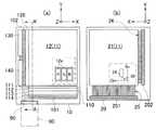
図1に示すように、液晶装置100は、互いに対向して配置された駆動回路基板(第1基板)10と、画素部形成基板(第2基板)20とを備えている。また、駆動回路基板10と画素部形成基板20とは、図3(a)に示すように、互いに対向する面の周縁部に設けられたシール材(接合材)52により接合されており、前記両基板10,20とシール材52とに囲まれて液晶層(電気光学物質層)50が封止されている。 As shown in FIG. 1, the
駆動回路基板10はその一辺端部において画素部形成基板20より外側に張り出しており、この張出し部10aには可撓性を有する配線基板であるフレキシブル基板80が接続されている。駆動回路基板10と画素部形成基板20とが平面的に重なる領域に、平面視矩形状の画像表示領域11が形成されており、画像表示領域11の隣接する2辺端に沿ってデータ線駆動回路110と走査線駆動回路120とが設けられている。画像表示領域11には、複数の画素が平面視マトリクス状に配列形成されている。 The
図2は、液晶装置100の電気的構成を説明するための回路構成図である。図2に示すように、液晶装置100は、画像表示領域11と、データ線駆動回路110と、走査線駆動回路120と、駆動回路110,120と電気的に接続されたタイミングジェネレータ(信号処理回路)130と、前記駆動回路110,120及びタイミングジェネレータ130と電気的に接続された電源回路140とを備えている。 FIG. 2 is a circuit configuration diagram for explaining an electrical configuration of the
液晶装置100は、駆動回路基板10と画素部形成基板20とを有しており、駆動回路基板10と画素部形成基板20とが導通領域181及び導通領域182を介して電気的に接続された構成を備えており、前記両基板が重なる領域に画像表示領域11が形成されている。 The
画像表示領域11には、互いに交差して延びる複数の走査線(G1,G2,G3,…,Gm)と、複数のデータ線(S1,S2,S3,…,Sn)とがそれぞれ配列形成されており、これら走査線とデータ線とによって区画される略矩形状の領域が液晶装置100の各画素に対応する。走査線とデータ線との各交差点に対応して画素スイッチング素子であるTFT(薄膜トランジスタ)30が設けられている。TFT30は、液晶50への電圧印加手段である画素電極24と電気的に接続されており、画素電極24とそれに対向する対向電極28との間に、液晶50が挟持されている。 In the
本実施形態の液晶装置100では、上記各部材のうち、走査線G1〜Gm、データ線S1〜Sn、TFT30、及び画素電極24は画素部形成基板20上に設けられて画素部21を構成している。一方、液晶50を介して画素電極24に対向する対向電極28は、駆動回路基板10上に形成されており、同じく駆動回路基板10にはデータ線駆動回路110及び走査線駆動回路120が設けられている。
そして、画素部形成基板20上に延在するデータ線S1〜Snは、それらの図示上側(−Y側)の端部に設けられた導通領域181において、駆動回路基板10上のデータ線駆動回路110から延びる配線と電気的に接続されている。また画素部形成基板20上に延在する前記走査線G1〜Gmは、それらの図示左側(−X側)の端部に設けられた導通領域182において、駆動回路基板10上の走査線駆動回路120から延びる配線と電気的に接続されている。In the
The data lines S1 to Sn extending on the pixel
液晶装置の各画素について走査線G1とデータ線S1との交差点に対応して設けられたTFT30を含む画素を挙げて説明すると、このTFT30のゲートは走査線G1と電気的に接続されており、TFT30のソースはデータ線S1と電気的に接続されている。TFT30のドレインは、液晶50への電圧印加手段である画素電極24と電気的に接続されている。画素電極24とそれに対向して設けられた対向電極28との間に液晶50が挟持されており、これら電極24,28間に印加された電圧に応じて画素の透過率が変化するようになっている。対向電極28には、電源回路140により生成された対向電極電位Vcomが供給されるようになっている。 For each pixel of the liquid crystal device, a pixel including the
データ線駆動回路110は、一水平走査単位の階調データ(画像信号)に基づいて、画像表示領域11のデータ線S1〜Snを順次走査駆動または一ライン毎もしくはグループ毎の駆動をする。走査線駆動回路120は、一垂直走査期間内に、水平同期信号に同期して、画像表示領域11の走査線G1〜Gmを順次走査駆動する。 The data
タイミングジェネレータ130は、本実施形態の場合、外部から入力されるビデオ信号やそれに同期したクロック信号から、液晶装置の動作に必要な各種信号(画像信号、制御信号)を生成する回路である。電源回路140は、外部から入力された単一ないし複数の電圧を液晶装置の駆動に必要な複数の電圧に変換する回路(DC−DCコンバータ)であり、データ線駆動回路110や走査線駆動回路120に供給する液晶駆動用電位や対向電極電位Vcomを生成する。 In the case of the present embodiment, the
図3(a)は、駆動回路基板10の液晶50側面(画素部形成基板20との対向面)を示す平面構成図であり、図3(b)は、画素部形成基板20の液晶50側面(駆動回路基板10との対向面)面を示す平面構成図である。
図3(a)に示す駆動回路基板10には、平面視矩形状のカラーフィルタ部12が設けられている。カラーフィルタ部12には、液晶装置100の各画素に対応する複数のカラーフィルタ12aが平面視マトリクス状に配列形成されている。カラーフィルタ部12の外側の基板上に、本発明に係る駆動回路部を構成するデータ線駆動回路110、走査線駆動回路120、タイミングジェネレータ130、及び電源回路140が配置されており、上記駆動回路部のうち、データ線駆動回路110と走査線駆動回路120とが、それぞれ画素部21に設けられたデータ線S1〜Sn及び走査線G1〜Gmに対して電気信号を供給する画素部駆動回路となっている。上記駆動回路部は駆動回路基板10上に形成されたポリシリコン膜(多結晶半導体層)を用いて形成されたものである。3A is a plan view showing the
A
カラーフィルタ部12の−X側の辺端に沿って、Y軸方向に長手の走査線駆動回路120が設けられている。走査線駆動回路120の外側に、走査側回路導通部(第1導通部)102が形成されており、走査側回路導通部102のさらに外側に、互いに電気的に接続されたタイミングジェネレータ130と電源回路140とが設けられている。走査側回路導通部102は、画素部形成基板20の画素部21と走査線駆動回路120との導電接続構造を形成するものであり、走査線駆動回路120と電気的に接続された多数の導通端子(走査側回路導通端子)を有している。 A scanning
走査線駆動回路120はシフトレジスタを含む回路であり、タイミングジェネレータ130から入力されるスタートパルスをそれとともに入力されるクロック信号に基づき順次シフトして走査線G1〜Gmに順次排他的に供給する。この走査線駆動回路120の動作により、複数のデータ線S1〜Snが、Y方向に線順次に選択される。 The scanning
カラーフィルタ部12の−Y側の辺端に沿って、X軸方向に長手のデータ線駆動回路110が設けられている。データ線駆動回路110の外側には、データ側回路導通部(第1導通部)101が形成されている。データ側回路導通部101は、画素部形成基板20の画素部21とデータ線駆動回路110との導電接続構造を形成するものであり、データ線駆動回路110と電気的に接続された多数の導通端子(データ側回路導通端子)を有している。 A data
データ線駆動回路110は、シフトレジスタ111と、ラッチ回路112と、DAコンバータ113と、アナログスイッチ114とを含んで構成されている。
シフトレジスタ111は、タイミングジェネレータ130から入力されるクロックに基づき、後段のラッチ回路112で画像信号を順次ラッチするタイミングをとるためのサンプリング信号を生成する回路である。ラッチ回路112は、タイミングジェネレータ130から入力される画像信号(6ビットRGB/シリアル)を一定時間保持する回路であり、シフトレジスタ111から入力されたサンプリング信号に同期して画像信号を取り込むことでドット単位の画像信号をライン単位に束ね、束ねた画像信号をDAコンバータ113に出力する。DAコンバータ113は、ラッチ回路112から入力されるライン単位の画像信号(デジタル信号)を液晶印加電圧(アナログ信号)に変換する回路である。アナログスイッチ114は、DAコンバータ113から入力される液晶印加電圧を決められたタイミングでデータ線S1〜Snに供給する回路である。The data line driving
The
駆動回路基板10の−Y側の辺端部には、外部接続端子90が形成されており、外部接続端子90には、駆動回路基板10上に形成された配線パターンを介して上記各回路(データ線駆動回路110、走査線駆動回路120、タイミングジェネレータ130、電源回路140)が電気的に接続されている。 An
図3(b)に示す画素部形成基板20には、平面視矩形状の画素部21が設けられている。画素部21には、液晶装置100の各画素に対応する複数の画素電極24が平面視マトリクス状に配列されており、各画素電極24に対応してTFT30が設けられている。また図2に示したように、互いに交差して延びる複数の走査線G1〜Gmと、複数のデータ線S1〜Snとが形成されており、各TFT30は対応する走査線及びデータ線とそれぞれ電気的に接続されている。 A pixel
画素部21の−X側の辺端部に沿って、Y軸方向に長手の走査側画素導通部(第2導通部)202が形成されており、走査側画素導通部202と画素部21(走査線G)とは、X軸方向に延びる配線群26を介して電気的に接続されている。走査側導通部202は、先に記載の走査側回路導通部102とともに、画素部21に延在する複数の走査線G1〜Gmと駆動回路基板10上の走査線駆動回路120との導電接続構造を形成するものであり、画素部21の各走査線G1〜Gmと電気的に接続された複数(m個)の導通端子(走査側画素導通端子)を備えている。 A scanning-side pixel conduction portion (second conduction portion) 202 that is long in the Y-axis direction is formed along the −X side edge of the
画素部21の−Y側の辺端部に沿って、X軸方向に長手のデータ側画素導通部(第2導通部)201が形成されており、データ側画素導通部201と画素部21(データ線S)とは、Y軸方向に延びる配線群25を介して電気的に接続されている。データ側画素導通部201は、先に記載のデータ側回路導通部101とともに、画素部21に延在する複数のデータ線S1〜Snとデータ線駆動回路110との導電接続構造を形成するものであり、画素部21の各データ線S1〜Snと電気的に接続された複数(n個)の導通端子(データ側回路導通端子)を備えている。 A data-side pixel conduction portion (second conduction portion) 201 that is long in the X-axis direction is formed along the −Y side edge of the
図4は、図3(a)のA−A’線に沿う液晶装置100の断面構成図である。図2に示した構成を具備した駆動回路基板10と画素部形成基板20とは、シール材52を介して接合されており、駆動回路基板10のカラーフィルタ部12と、画素部形成基板20の画素部21とが互いに対向して配置されている。また、液晶50の図示左側に符号181を付して示す導通領域が設けられており、当該導通領域181には、駆動回路基板10のデータ側回路導通部101と、画素部形成基板20のデータ側画素導通部201とが平面的に重なるように配置されている。そして、これらの導通部101,201間に設けられた導電部材190によって、データ側回路導通部101とデータ側画素導通部201とが電気的に接続されている。これにより、駆動回路基板10上のデータ線駆動回路110と、画素部21(データ線S1〜Sn)とが電気的に接続されている。 FIG. 4 is a cross-sectional configuration diagram of the
図5は、画素部形成基板20側からみた上記導通領域181の平面構造を示す説明図である。図5に示すように、同領域には複数のデータ側回路導通端子101aと、複数のデータ側画素導通端子201aとがX軸方向に沿って配列されている。各データ側回路導通端子101aは、データ線駆動回路110と電気的に接続されており、各データ側画素導通端子201aは、画素部21(より詳細には当該データ側画素導通端子201aに対応する走査線S1〜Sn)と電気的に接続されている。 FIG. 5 is an explanatory diagram showing a planar structure of the
そして、図5に示すように、導通領域181において、各データ側回路導通端子101aと各データ側画素導通端子201aとが平面的に重なって配置されており、複数の導通端子101a、201aに跨ってX軸方向に延在する導電部材190の導電粒子185のうち、前記導通端子101a、201a間に挟まれたものが両導通端子101a、201aを電気的に接続している。その余の導電粒子185は、導通端子間の電気的接続に寄与せず、したがってX軸方向に関して隣接する導通端子101a、201aが短絡しない構造となっている。 As shown in FIG. 5, in the
本実施形態の場合、導通部材190は、絶縁性ペーストからなるマトリクス186中に導電粒子185を分散させた異方性導電ペーストであり、導電粒子185は、表面に金属膜が被覆された樹脂粒子や金属粒子である。そして、上記異方性導電ペーストは、駆動回路基板10と画素部形成基板20との貼り合わせに際して、導通部101上又は導通部201上に選択的に塗布され、基板10,20を貼り合わせることで導電粒子185が互いに対向する導通端子101a及び導通端子201aに接触し、両者を導通するようになっている。 In this embodiment, the
なお、導電部材190としては、上記異方性導電ペーストに限らず、異方性導電フィルム(導電粒子を内部に分散させたフィルム)も問題なく用いることができる。また本実施形態では導通領域181(導電部材190)をシール材52の内側(液晶50側)に設けているが、導通領域181をシール材52の外側に設けてもよいのは勿論である。シール材52の外側に導電部材190を配置すれば、液晶と接触させることが不適切な材質の導電部材190であっても問題なく適用できる。
またさらに、導電部材190はシール材52の一部を成すものであってもよい。つまり、シール材52として導電粒子が内部に分散されたものを用いてもよい。このような構成とすれば、シール材形成領域にて駆動回路基板10と画素部形成基板20との電気的接続が可能になり、液晶装置100の狭額縁化に有利な構成となる。The
Furthermore, the
また図3には表れていないが、図3に示した駆動回路基板10の走査側回路導通部102と、画素部形成基板20の走査側画素導通部202とは、図2に示した導通領域182において平面的に重なって配置されており、当該領域で導電部材を介して電気的に接続されている。具体的には、図5に示した導通領域181と同様に、走査側回路導通部102を構成する各走査側回路導通端子に対して、走査側画素導通部202を構成する各走査側画素導通端子が位置合わせされて配置され、Z軸方向で対向する導通端子同士が、図4に示したのと同様の導電部材を介して電気的に接続されている。このような構造により、走査線駆動回路120と、画素部21(走査線G1〜Gm)とが電気的に接続されている。 Although not shown in FIG. 3, the scanning-side
上記構成を具備した本実施形態の液晶装置100によれば、駆動回路部(データ線駆動回路110、走査線駆動回路120、タイミングジェネレータ130、及び電源回路140)と、画素部21とを異なる基板上に形成した構成により、駆動回路基板10と画素部形成基板20の双方で高い性能が得られ、また高歩留まりに製造することが可能になっている。
すなわち、画素部と駆動回路部とを同一の基板上に形成する場合では、製造効率上、駆動回路部と画素部とを同工程で並行して形成することが好ましいが、このような製造方法では、駆動回路部の形成と画素部の形成の双方に最適な工程を適用するのが極めて困難である。
これに対して本実施形態の液晶装置では、駆動回路部の形成と画素部の形成とにそれぞれ最適な製造工程を適用できる。駆動回路110,120等を備えた駆動回路基板10では最小線幅の細いフォトリソグラフィ工程を適用して高性能の回路を形成することができる一方、比較的大きな面積での品質の均一性が要求される画素部21では、最小線幅は細くないが大型基板への均一な加工が可能なフォトリソグラフィ工程を適用して画素間で均一なスイッチング特性を得ることができ、輝度、コントラスト等の均一性に優れる表示を得ることができる。According to the
That is, when the pixel portion and the drive circuit portion are formed on the same substrate, it is preferable to form the drive circuit portion and the pixel portion in parallel in the same process in terms of manufacturing efficiency. Therefore, it is extremely difficult to apply an optimal process to both the formation of the drive circuit portion and the formation of the pixel portion.
On the other hand, in the liquid crystal device of the present embodiment, optimum manufacturing processes can be applied to the formation of the drive circuit portion and the formation of the pixel portion, respectively. In the
また駆動回路基板10と画素部形成基板20とは別々の工程で製造されるので、最小線幅が狭く、加工に時間の掛かるフォトリソグラフィ工程を駆動回路基板10の製造に適用したとしても、液晶装置100全体の製造時間への影響を抑えることが可能である。 In addition, since the
さらに、画素部形成基板20の画素部21に用いられる画素スイッチング素子としては、ポリシリコンを半導体層に用いたTFTに限られず、アモルファスシリコン(非晶質シリコン)を半導体層に用いたTFTであってもよい。アモルファスシリコンTFTを画素スイッチング素子に用いることで、比較的大型の液晶装置100であっても低コストに製造できる。
なお、本実施形態では液晶50の層厚方向両側にそれぞれ電極(画素電極24、対向電極28)が設けられた構成の液晶装置について説明したが、本発明に係る液晶装置は、このようなTN(Twisted Nematic)モードやVAN(Vertical Aligned Nematic)モードに好適な構成に限らず、IPS(In-Plane Switching)方式やFFS(Fringe Field Switching)方式と呼ばれている横電界モードの液晶装置としても構成とすることができる。この場合、図2に示した対向電極28は、駆動回路基板10上ではなく画素部形成基板20側に設けられることとなる。Further, the pixel switching element used in the
In the present embodiment, the liquid crystal device having the configuration in which the electrodes (
あるいはまた、本実施形態の液晶装置100は、パッシブマトリクス型の液晶装置として構成することも可能である。この場合、画素部形成基板20は、その画素部21に平面視短冊状の透明電極がストライプ状に配列形成された構成とされ、駆動回路基板10は、前記画素部21と対向する領域に上記画素部21の透明電極と交差する方向に延びる短冊状の透明電極がストライプ状に配列形成された構成とされる。 Alternatively, the
なお、本実施形態では、駆動回路基板10上にカラーフィルタ部12を形成しているが、カラーフィルタ部12を画素部形成基板20上に形成してもよいのは勿論である。駆動回路基板10上に設けた駆動回路部は静電気耐性が高くないので、カラーフィルタ部12の形成工程が駆動回路部に影響するものであるなら、カラーフィルタ部12は画素部形成基板20側に設けるのがよい。 In this embodiment, the
(液晶装置の製造方法)
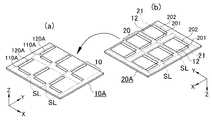
次に、上記実施形態の液晶装置100の製造方法について図6を参照して以下に説明する。
図6(a)は、複数の駆動回路基板10を一括に形成する大型駆動回路基板10Aを示す斜視構成図であり、図6(b)は、複数の画素部形成基板20を一括に形成する大型画素部形成基板20Aを示す斜視構成図である。なお、本実施形態では大型基板の例として6枚取りのものを示しているが、これに限られるものではない。(Manufacturing method of liquid crystal device)
Next, a method for manufacturing the
FIG. 6A is a perspective configuration diagram showing a large
<駆動回路基板>
図6(a)に示す大型駆動回路基板10Aは、駆動回路基板10となるべき6個の矩形状領域を形成できる大型のガラス基板を基体としている。符号SLを付して示す点線はスクライブラインであり、スクライブラインSLにより区画された各領域が図示の大型ガラス基板における駆動回路基板10の形成領域である。<Drive circuit board>
A large
まず、上記大型ガラス基板の一面(+Z側面)に、平面視略矩形状のポリシリコン膜110A、120Aをパターン形成する。これらのポリシリコン膜110A、120Aは、大型ガラス基板に非晶質シリコン膜を形成した後、非晶質シリコン膜にレーザーを照射することで結晶化して得られたものであり、いわゆる低温ポリシリコン技術を用いて形成したものである。 First,
低温ポリシリコン技術とは、従来の基板を高温(1000℃程度)に加熱してポリシリコン膜を得る技術に対し、600℃以下の低温プロセスでポリシリコン膜を得る技術である。上記レーザー照射により非晶質シリコン膜を結晶化する技術では、レーザーを照射する工程を常温で行うことができるため、非晶質シリコン膜の脱水素処理工程や不純物活性化工程の温度(600℃程度)を超えないプロセス温度での製造が可能になる。
また低温ポリシリコン技術としてはNi助長固相成長法と呼ばれる技術も知られており、この技術においても非晶質シリコンを加熱して結晶化する際の温度を抑えることができるため、非晶質シリコン膜の脱水素処理工程やNiゲッタリング工程を含めても600℃以下のプロセス温度で製造することができる。The low-temperature polysilicon technology is a technology for obtaining a polysilicon film by a low-temperature process of 600 ° C. or lower as compared with a technology for obtaining a polysilicon film by heating a conventional substrate to a high temperature (about 1000 ° C.). In the technique of crystallizing an amorphous silicon film by the laser irradiation, the laser irradiation process can be performed at room temperature, so the temperature of the amorphous silicon film dehydrogenation process and impurity activation process (600 ° C. Manufacturing at a process temperature not exceeding (about).
As a low-temperature polysilicon technique, a technique called Ni-assisted solid-phase growth method is also known. In this technique, the temperature at which amorphous silicon is heated to be crystallized can be suppressed. Even if a silicon film dehydrogenation process and a Ni gettering process are included, it can be manufactured at a process temperature of 600 ° C. or less.
図6(a)に示すように、ポリシリコン膜110A、120Aは大型ガラス基板上の領域に部分的に形成され、その占有面積も小さいため、上記非晶質ポリシリコン膜に対するレーザー照射は、ポリシリコン膜を形成すべき領域に限定して行えばよい。このようにレーザー照射領域を限定すれば、レーザー照射工程におけるスループットを向上させることができる。あるいは、小領域に限定してレーザー照射が可能なので、単位面積あたりのレーザー照射時間を長くとることができ、欠陥の少ないポリシリコンの膜が得られる。 As shown in FIG. 6A, the
次に、上記ポリシリコン膜110A、120Aを用いてトランジスタやダイオード、キャパシタ等を形成することにより、図3に示したデータ線駆動回路110、走査線駆動回路120、タイミングジェネレータ130、及び電源回路140からなる駆動回路部を大型ガラス基板上に形成する。これらの具体的な製造方法については、公知の製造方法が適用できるので省略する。また、上記駆動回路部を構成する金属配線や電極等とともに、複数の導通端子を大型ガラス基板上に形成し、データ側回路導通部101及び走査側回路導通部102を形成する。 Next, transistors, diodes, capacitors, and the like are formed using the
上記駆動回路部の形成工程では、ポリシリコン膜110A、120Aに対して部分的な不純物導入及び活性化を行うが、本実施形態の製造方法では、この不純物活性化工程をレーザー照射により行ってもよい。従来は、不純物活性化はファーネス(炉)やランプアニール(RTA)で行っていたが、レーザー照射により不純物活性化を行うことで、高い活性化率と欠陥修復性とが得られる。この場合にも、大型ガラス基板上に部分的に形成されたポリシリコン膜110A、120Aのみに対してレーザー照射を行えばよいので、効率よく迅速に不純物活性化工程を実行することができる。 In the formation process of the drive circuit portion, partial impurity introduction and activation are performed on the
また、駆動回路部を形成する工程は、画素部21を形成する工程とは独立に行われるので、駆動回路部を構成する配線材料や回路の構成材料について、画素部21の構成によらず、任意に選択することが可能である。したがって、上記配線材料等として、上記レーザー照射による不純物活性化を行うのに最適な材料を選択することができ、安価な材料を用いつつ不純物活性化を良好に行うことが可能になる。さらに、配線や電極の膜厚や、配線層間に設けられる層間絶縁膜の膜厚についても、画素部21の構成によらず任意に設定可能であるため、高性能回路の製造が容易になる。さらに、液晶を挟持する二枚の基板のみを利用するのでコストの高い別基板の部材を必要とせず、しかもICやLSIと同様なシステム回路を液晶装置に搭載しているので、コストの高いICやLSIを外付けする必要もない。 In addition, since the process of forming the drive circuit unit is performed independently of the process of forming the
次に、駆動回路部(データ線駆動回路110、走査線駆動回路120、タイミングジェネレータ130、及び電源回路140)が形成された大型駆動回路基板10A上に、上記駆動回路部に隣接してカラーフィルタ部12を形成する。カラーフィルタ部12の形成に際しては公知の製造方法を用いることができ、例えば印刷法や液滴吐出法を用いてカラーフィルタ部12を形成することができる。
以上の工程により、大型駆動回路基板10Aが得られる。Next, on the large-sized
The large
<画素部形成基板>
次に画素部形成基板20の製造工程について説明する。
図6(b)に示すように、画素部形成基板20の製造にも、6枚の画素部形成基板20を一括に製造可能な大型ガラス基板が用いられる。スクライブラインSLに囲まれる各領域が画素部形成基板20の形成領域である。大型画素部形成基板20Aの図示上面(−Z側面)には、複数の画素部21と、各画素部21から延出されたデータ側画素導通部201と走査側画素導通部202とが形成される。<Pixel part formation substrate>
Next, a manufacturing process of the pixel
As shown in FIG. 6B, a large glass substrate capable of manufacturing six pixel
画素部形成基板20Aの製造には、従来から知られているTFTアクティブマトリクス基板の製造方法がそのまま適用できる。すなわち、大型ガラス基板上に非晶質シリコン膜、あるいは非晶質シリコン膜を結晶化してなるポリシリコン膜を形成し、これらを半導体層とするTFTを大型ガラス基板上に配列形成する。その後TFTと電気的に接続された画素電極を大型ガラス基板上に平面視マトリクス状に配列形成することで、画素部21を形成することができる。 For manufacturing the pixel
また、データ側画素導通部201については、上記画素部21のTFTと接続されて画素部21内に延在する複数のデータ線を画素部21の外側(−Y側)まで延出することで形成でき、走査側画素導通部202については、画素部21のTFTと接続されて画素部21内に延在する複数の走査線を画素部21の外側(−X側)まで延出することで形成することができる。導通部201,202を構成する各導通端子の先端部については、図5に示したデータ側画素導通端子201aのように拡幅してパッドを形成しておくのがよい。
以上の工程により大型画素部形成基板20Aが得られる。For the data-side
The large pixel
大型駆動回路基板10Aと大型画素部形成基板20Aとを製造したならば、図6に示すように、大型駆動回路基板10Aの図示上面(+Z側面)と大型画素部形成基板20Aの図示上面(−Z側面)とを対向させて貼り合わせる。貼り合わせに際しては、図3に示したように、各画素部形成基板20の形成領域の周縁部に平面視略矩形状のシール材52を配置しておく。またデータ側回路導通部101とデータ側画素導通部201とが対向する領域、及び走査側回路導通部102と走査側画素導通部202とが対向する領域に、異方性導電ペースト等からなる導電部材190を配置しておく。 When the large
なお、シール材52により駆動回路基板10と画素部形成基板20との間に封止される液晶は、上記貼り合わせに先立って大型駆動回路基板10A又は大型画素部形成基板20A上に選択的に配置してもよいし、基板を貼り合わせた後にシール材52の内側に注入してもよい。またシール材52及び導電部材190を配置する基板は大型画素部形成基板20Aでなくても構わない。 Note that the liquid crystal sealed between the
上記貼り合わせ工程によって、データ側回路導通部101とデータ側画素導通部201とが導電部材190により電気的に接続され、また走査側回路導通部102と走査側画素導通部202とが導電部材190により電気的に接続される。その結果、大型駆動回路基板10A上のデータ線駆動回路及び走査線駆動回路と、大型画素部形成基板20A上の画素部21とが電気的に接続される。
その後、大型駆動回路基板10A、及び大型画素部形成基板20AのスクライブラインSLに沿ってガラス基板を切断することで、6個の液晶装置100を製造することができる。Through the bonding step, the data side
Thereafter, the six
本実施形態の製造方法では、大型駆動回路基板10Aと大型画素部形成基板20Aとを別々の工程で製造するので、大型駆動回路基板10Aの製造に際しては、最小線幅の細い微細加工が可能なフォトリソグラフィ工程を適用して高集積、高性能の駆動回路部を形成することができる一方、大型画素部形成基板20Aの製造に際しては、大型ガラス基板の全面で均一な加工が可能なフォトリソグラフィ工程を適用して、電気特性のばらつきが少ない画素スイッチング素子を具備した画素部21を形成することができる。したがって本製造方法によれば、高性能の駆動回路部を備え、均一な表示画像が得られる液晶装置を歩留まりよく製造することができる。 In the manufacturing method of the present embodiment, the large
また、大型駆動回路基板10Aの製造に際して、大型ガラス基板上に形成した非晶質シリコン膜に対し部分的にレーザー照射を行うことでポリシリコン膜110A、120Aを形成することができるので、ポリシリコン膜の形成工程を迅速かつ効率的に行うことができる。またこのように部分的にレーザー照射を行う場合には大型のレーザー装置は不要で、安価な小型レーザー装置を用いることができるので、設備コストの点でも有利である。
さらにポリシリコン膜110A、120Aに注入した不純物の活性化に際してもレーザー照射を用いることができ、図6に示すように、画素部形成基板20の製造にも、6枚の画素部形成基板20を一括に製造可能な大型ガラス基板が用いられる。図6(b)のスクライブラインSLに囲まれる各領域が画素部形成基板20の形成領域である。この不純物活性化工程においても、ポリシリコン膜110A、120Aに対して選択的にレーザー照射を行うこととすれば、高いスループットで不純物活性化を行うことができる。Further, when manufacturing the large
Furthermore, laser irradiation can also be used when activating the impurities implanted into the
また、データ線駆動回路110、走査線駆動回路120等の駆動回路部と、画素部21のそれぞれで最適な構成材料を選択することができるので、例えば駆動回路部については上記レーザー照射による不純物活性化に適した構成材料を用いて配線や電極を形成することができる。 Further, since the optimum constituent material can be selected for each of the driving circuit unit such as the data
(製造方法の変形例)
先に記載のように、本発明に係る液晶装置においては、カラーフィルタ部12を駆動回路基板10と画素部形成基板20のいずれに設けるかは選択的であり、図6を参照して説明した上記製造方法では、大型駆動回路基板10Aにカラーフィルタ部12を設けることとしていた。以下では、カラーフィルタ部12を大型画素部形成基板20Aに設ける場合の製造工程について説明する。なお、上記カラーフィルタ部12の配置以外は図6に示した製造方法と同様であるから、図7において図6と共通の構成要素には同一の符号を付して説明を省略する。(Modification of manufacturing method)
As described above, in the liquid crystal device according to the present invention, it is optional to provide the
図7に示すように、本実施形態の製造方法では、大型駆動回路基板10Aではなく大型画素部形成基板20A上にカラーフィルタ部12を形成する。すなわち、図6に示した大型画素部形成基板20Aの画素部21上に、さらにカラーフィルタ部12を積層して形成する。一方、大型駆動回路基板10Aでは、データ線駆動回路110、走査線駆動回路120、タイミングジェネレータ130、及び電源回路140からなる駆動回路部の形成工程までを行う。 As shown in FIG. 7, in the manufacturing method of this embodiment, the
本製造方法によれば、カラーフィルタ部12を駆動回路基板10と異なる基板上に形成するので、低温ポリシリコン膜を用いて形成しているために比較的静電気耐性の低い駆動回路部が形成されている大型駆動回路基板10Aをさらに他の工程に供する必要が無くなり、駆動回路部に対する静電気等の影響を可能な限り排除できる。したがって本製造方法は、液晶装置の歩留まり向上に大きく寄与し得るものである。 According to this manufacturing method, since the
(電子機器)
図8は、本発明に係る電子機器の一例を示す斜視図である。図8に示す携帯電話1300は、上記実施形態の液晶装置を小サイズの表示部1301として備え、複数の操作ボタン1302、受話口1303、及び送話口1304を備えて構成されている。
上記各実施の形態の液晶装置は、上記携帯電話に限らず、電子ブック、プロジェクタ、パーソナルコンピュータ、ディジタルスチルカメラ、テレビジョン受像機、ビューファインダ型あるいはモニタ直視型のビデオテープレコーダ、カーナビゲーション装置、ページャ、電子手帳、電卓、ワードプロセッサ、ワークステーション、テレビ電話、POS端末、タッチパネルを備えた機器等々の画像表示手段として好適に用いることができ、かかる構成とすることで、高機能の駆動回路をパネルに実装し、制御性に優れ、またコンパクトで実装性に優れた表示部を具備した電子機器を実現できる。(Electronics)
FIG. 8 is a perspective view showing an example of an electronic apparatus according to the present invention. A
The liquid crystal device of each of the above embodiments is not limited to the mobile phone, but an electronic book, a projector, a personal computer, a digital still camera, a television receiver, a viewfinder type or a monitor direct view type video tape recorder, a car navigation device, It can be suitably used as image display means for devices such as pagers, electronic notebooks, calculators, word processors, workstations, videophones, POS terminals, touch panels, etc. With such a configuration, a high-performance drive circuit can be used as a panel Therefore, it is possible to realize an electronic device including a display unit that is excellent in controllability, compact, and excellent in mountability.
なお、本発明の技術範囲は、上述した各実施形態に限定されるものではなく、本発明の趣旨を逸脱しない範囲において、上述した各実施形態に種々の変更を加えたものを含む。すなわち、各実施形態で挙げた具体的な材料や構成などはほんの一例に過ぎず、適宜変更が可能である。例えば、上記実施形態では電気光学装置の一例として液晶装置を挙げて説明したが、画素部と該画素部に接続された駆動回路部とを具備した電気光学装置であれば本発明は問題なく適用でき、例えば、有機エレクトロルミネッセンス装置、プラズマ型装置にも好適に用いることができる。 The technical scope of the present invention is not limited to the above-described embodiments, and includes various modifications made to the above-described embodiments without departing from the spirit of the present invention. That is, the specific materials and configurations described in the embodiments are merely examples, and can be changed as appropriate. For example, in the above-described embodiment, a liquid crystal device has been described as an example of an electro-optical device. However, the present invention can be applied without any problem as long as the electro-optical device includes a pixel portion and a drive circuit portion connected to the pixel portion. For example, it can be suitably used for an organic electroluminescence device and a plasma type device.
100 液晶装置(電気光学装置)、10 駆動回路基板(第1基板)、12 カラーフィルタ部、20 画素部形成基板(第2基板)、21 画素部、24 画素電極、28 対向電極、30 TFT(薄膜トランジスタ)、50 液晶層、52 シール材、80 フレキシブル基板、90 外部接続端子、101 データ側回路導通部(第1導通部)、101a データ側回路導通端子、102 走査側回路導通部(第1導通部)、201 データ側画素導通部(第2導通部)、201a データ側画素導通端子、202 走査側画素導通部(第2導通部)、110 データ線駆動回路、120 走査線駆動回路、130 タイミングジェネレータ、140 電源回路、111 シフトレジスタ、112 ラッチ回路、113 DAコンバータ、114 アナログスイッチ、181,182 導通領域、190 導電部材 100 liquid crystal device (electro-optical device), 10 drive circuit substrate (first substrate), 12 color filter portion, 20 pixel portion forming substrate (second substrate), 21 pixel portion, 24 pixel electrode, 28 counter electrode, 30 TFT ( Thin film transistor), 50 liquid crystal layer, 52 sealing material, 80 flexible substrate, 90 external connection terminal, 101 data side circuit conduction part (first conduction part), 101a data side circuit conduction terminal, 102 scanning side circuit conduction part (first conduction) Part), 201 data side pixel conduction part (second conduction part), 201a data side pixel conduction terminal, 202 scanning side pixel conduction part (second conduction part), 110 data line driving circuit, 120 scanning line driving circuit, 130 timing Generator, 140 Power supply circuit, 111 Shift register, 112 Latch circuit, 113 DA converter, 114A Analog switch, 181 and 182 Conductive region, 190 Conductive member
Claims (11)
Translated fromJapanese前記第1基板の前記第2基板との対向面に、多結晶半導体層を含む駆動回路部と、該駆動回路部に導電接続された第1導通部とが設けられ、
前記第2基板の前記第1基板との対向面には、画素電極と、該画素電極に導電接続された第2導通部とが設けられており、
前記第1導通部と第2導通部とが、互いに平面的に重なる領域で電気的に接続されていることを特徴とする電気光学装置。A first substrate and a second substrate disposed opposite to each other;
A driving circuit unit including a polycrystalline semiconductor layer and a first conductive unit electrically connected to the driving circuit unit are provided on a surface of the first substrate facing the second substrate,
A surface of the second substrate facing the first substrate is provided with a pixel electrode and a second conductive portion conductively connected to the pixel electrode,
The electro-optical device, wherein the first conductive portion and the second conductive portion are electrically connected in a region overlapping each other in a plane.
前記第1導通部の導通端子と第2導通部の導通端子とが、前記第1基板と第2基板との間に設けられた異方性導電材料を介して電気的に接続されていることを特徴とする請求項3又は4に記載の電気光学装置。A plurality of conduction terminals are provided in each of the first conduction part and the second conduction part,
The conduction terminal of the first conduction part and the conduction terminal of the second conduction part are electrically connected via an anisotropic conductive material provided between the first substrate and the second substrate. The electro-optical device according to claim 3 or 4.
前記第2導通部が、前記複数の走査線と電気的に接続された複数の走査側画素導通端子と、前記複数のデータ線と電気的に接続された複数のデータ側画素導通端子とを含んでおり、
前記第1基板の駆動回路部が、前記走査線に電気信号を供給する走査線駆動回路と、前記データ線に電気信号を供給するデータ線駆動回路とを含み、
前記第1導通部が、前記走査線駆動回路と電気的に接続された複数の走査側回路導通端子と、前記データ線駆動回路と電気的に接続された複数のデータ側回路導通端子とを有しており、
前記走査側画素導通端子と前記走査側回路導通端子とが電気的に接続され、前記データ側画素導通端子と前記データ側回路導通端子とが電気的に接続されていることを特徴とする請求項1から8のいずれか1項に記載の電気光学装置。A plurality of scanning lines and a plurality of data lines extending across the second substrate are formed on the second substrate, and are electrically connected to the pixel electrodes corresponding to the intersections of the scanning lines and the data lines. A thin film transistor is provided,
The second conduction part includes a plurality of scanning-side pixel conduction terminals electrically connected to the plurality of scanning lines, and a plurality of data-side pixel conduction terminals electrically connected to the plurality of data lines. And
The driving circuit unit of the first substrate includes a scanning line driving circuit for supplying an electric signal to the scanning line; and a data line driving circuit for supplying an electric signal to the data line;
The first conduction unit has a plurality of scanning side circuit conduction terminals electrically connected to the scanning line driving circuit and a plurality of data side circuit conduction terminals electrically connected to the data line driving circuit. And
The scanning side pixel conduction terminal and the scanning side circuit conduction terminal are electrically connected, and the data side pixel conduction terminal and the data side circuit conduction terminal are electrically connected. The electro-optical device according to any one of 1 to 8.
第2基板の一面に、画素電極と、該画素電極に導電接続された第2導通部とを形成する工程と、
前記第1基板の第1導通部と前記第2基板の第2導通部とを対向させて前記第1基板と第2基板とを貼り合わせることで前記第1導通部と前記第2導通部とを電気的に接続する工程と、
を有することを特徴とする電気光学装置の製造方法。Forming a driving circuit portion including a polycrystalline semiconductor layer on one surface of the first substrate and a first conduction portion conductively connected to the driving circuit portion;
Forming a pixel electrode and a second conductive portion conductively connected to the pixel electrode on one surface of the second substrate;
The first conductive portion and the second conductive portion are bonded by bonding the first substrate and the second substrate with the first conductive portion of the first substrate facing the second conductive portion of the second substrate. Electrically connecting
A method for manufacturing an electro-optical device.
Priority Applications (2)
| Application Number | Priority Date | Filing Date | Title |
|---|---|---|---|
| JP2005063423AJP2006250984A (en) | 2005-03-08 | 2005-03-08 | Electrooptical apparatus, manufacturing method for the same and electronic equipment |
| US11/330,306US20060202931A1 (en) | 2005-03-08 | 2006-01-11 | Electro-optical device, method of manufacturing electro-optical device, and electronic apparatus |
Applications Claiming Priority (1)
| Application Number | Priority Date | Filing Date | Title |
|---|---|---|---|
| JP2005063423AJP2006250984A (en) | 2005-03-08 | 2005-03-08 | Electrooptical apparatus, manufacturing method for the same and electronic equipment |
Publications (1)
| Publication Number | Publication Date |
|---|---|
| JP2006250984Atrue JP2006250984A (en) | 2006-09-21 |
Family
ID=36970284
Family Applications (1)
| Application Number | Title | Priority Date | Filing Date |
|---|---|---|---|
| JP2005063423APendingJP2006250984A (en) | 2005-03-08 | 2005-03-08 | Electrooptical apparatus, manufacturing method for the same and electronic equipment |
Country Status (2)
| Country | Link |
|---|---|
| US (1) | US20060202931A1 (en) |
| JP (1) | JP2006250984A (en) |
Cited By (1)
| Publication number | Priority date | Publication date | Assignee | Title |
|---|---|---|---|---|
| JP2008112057A (en)* | 2006-10-31 | 2008-05-15 | Fuji Xerox Co Ltd | Image display medium and image display system |
Families Citing this family (4)
| Publication number | Priority date | Publication date | Assignee | Title |
|---|---|---|---|---|
| KR101957998B1 (en) | 2012-06-20 | 2019-07-03 | 삼성디스플레이 주식회사 | Display panel and method of fabricating the same |
| US9948346B2 (en)* | 2012-11-01 | 2018-04-17 | Mediatek Inc. | Communication system with up-converter and digital baseband processing circuit implemented in one die separated from another die having down-converter, and related communication method thereof |
| TWI671581B (en)* | 2018-02-27 | 2019-09-11 | 鴻海精密工業股份有限公司 | Light emitting diode display device and pixel mounting method |
| CN110288942B (en)* | 2019-06-28 | 2020-12-29 | 上海天马有机发光显示技术有限公司 | Display panel and display device |
Family Cites Families (5)
| Publication number | Priority date | Publication date | Assignee | Title |
|---|---|---|---|---|
| JPS58182685A (en)* | 1982-04-20 | 1983-10-25 | セイコーエプソン株式会社 | Vertical energization agent for display panel |
| JP3184853B2 (en)* | 1993-06-24 | 2001-07-09 | 株式会社日立製作所 | Liquid crystal display |
| US5757456A (en)* | 1995-03-10 | 1998-05-26 | Semiconductor Energy Laboratory Co., Ltd. | Display device and method of fabricating involving peeling circuits from one substrate and mounting on other |
| US6501525B2 (en)* | 2000-12-08 | 2002-12-31 | Industrial Technology Research Institute | Method for interconnecting a flat panel display having a non-transparent substrate and devices formed |
| JP2005181830A (en)* | 2003-12-22 | 2005-07-07 | Seiko Epson Corp | Electro-optical device and electronic apparatus |
- 2005
- 2005-03-08JPJP2005063423Apatent/JP2006250984A/enactivePending
- 2006
- 2006-01-11USUS11/330,306patent/US20060202931A1/ennot_activeAbandoned
Cited By (1)
| Publication number | Priority date | Publication date | Assignee | Title |
|---|---|---|---|---|
| JP2008112057A (en)* | 2006-10-31 | 2008-05-15 | Fuji Xerox Co Ltd | Image display medium and image display system |
Also Published As
| Publication number | Publication date |
|---|---|
| US20060202931A1 (en) | 2006-09-14 |
Similar Documents
| Publication | Publication Date | Title |
|---|---|---|
| JP4367542B2 (en) | Electro-optical device and electronic apparatus | |
| CN103869562B (en) | Liquid crystal display device | |
| KR102034112B1 (en) | Liquid crystal display device and method of driving the same | |
| WO2007135893A1 (en) | Display device | |
| CN1928639A (en) | Electro-optical devices, electronic equipment, and interface substrates | |
| WO2018112997A1 (en) | Goa circuit structure | |
| CN100414402C (en) | LCD Monitor | |
| KR101604492B1 (en) | Liquid Crystal Display device | |
| WO2011052258A1 (en) | Display panel and display apparatus | |
| US20060202931A1 (en) | Electro-optical device, method of manufacturing electro-optical device, and electronic apparatus | |
| CN101561609A (en) | Active array substrate, liquid crystal display panel and method for manufacturing active array substrate | |
| KR100781104B1 (en) | Electro-optical device, method of manufacturing electro-optical device, and electronic apparatus | |
| TWI439778B (en) | Pixel array substrate and display panel | |
| US9651836B2 (en) | Display device | |
| JP4469146B2 (en) | Display device | |
| KR20150001168A (en) | Thin Film Transistor Substrate For Flat Panel Display Having Additional Common Line | |
| JP3645667B2 (en) | Liquid crystal display | |
| KR100990315B1 (en) | LCD Display | |
| JP2004037956A (en) | Liquid crystal display and its drive circuit | |
| JP2000047259A (en) | Liquid crystal display | |
| JP3251391B2 (en) | Image display device | |
| US20060256064A1 (en) | Liquid crystal display device | |
| JP2005300920A (en) | Display device and liquid crystal display | |
| JPH10282522A (en) | Display device | |
| JP2008172117A (en) | Electrooptic device, board for electrooptic device, semiconductor element and electronic apparatus |
Legal Events
| Date | Code | Title | Description |
|---|---|---|---|
| RD04 | Notification of resignation of power of attorney | Free format text:JAPANESE INTERMEDIATE CODE: A7424 Effective date:20070403 | |
| A977 | Report on retrieval | Free format text:JAPANESE INTERMEDIATE CODE: A971007 Effective date:20080829 | |
| A131 | Notification of reasons for refusal | Free format text:JAPANESE INTERMEDIATE CODE: A131 Effective date:20080924 | |
| A521 | Written amendment | Free format text:JAPANESE INTERMEDIATE CODE: A523 Effective date:20081118 | |
| A02 | Decision of refusal | Free format text:JAPANESE INTERMEDIATE CODE: A02 Effective date:20090127 |