JP2006245589A - Transistor using physical property conversion layer, and operation and manufacturing method thereof - Google Patents
Transistor using physical property conversion layer, and operation and manufacturing method thereofDownload PDFInfo
- Publication number
- JP2006245589A JP2006245589AJP2006056765AJP2006056765AJP2006245589AJP 2006245589 AJP2006245589 AJP 2006245589AJP 2006056765 AJP2006056765 AJP 2006056765AJP 2006056765 AJP2006056765 AJP 2006056765AJP 2006245589 AJP2006245589 AJP 2006245589A
- Authority
- JP
- Japan
- Prior art keywords
- film
- conductive layer
- layer pattern
- physical property
- transistor
- Prior art date
- Legal status (The legal status is an assumption and is not a legal conclusion. Google has not performed a legal analysis and makes no representation as to the accuracy of the status listed.)
- Pending
Links
Images


Classifications
- H—ELECTRICITY
- H10—SEMICONDUCTOR DEVICES; ELECTRIC SOLID-STATE DEVICES NOT OTHERWISE PROVIDED FOR
- H10D—INORGANIC ELECTRIC SEMICONDUCTOR DEVICES
- H10D30/00—Field-effect transistors [FET]
- H10D30/60—Insulated-gate field-effect transistors [IGFET]
- H10D30/67—Thin-film transistors [TFT]
- H10D30/674—Thin-film transistors [TFT] characterised by the active materials
- H10D30/6755—Oxide semiconductors, e.g. zinc oxide, copper aluminium oxide or cadmium stannate
- A—HUMAN NECESSITIES
- A47—FURNITURE; DOMESTIC ARTICLES OR APPLIANCES; COFFEE MILLS; SPICE MILLS; SUCTION CLEANERS IN GENERAL
- A47F—SPECIAL FURNITURE, FITTINGS, OR ACCESSORIES FOR SHOPS, STOREHOUSES, BARS, RESTAURANTS OR THE LIKE; PAYING COUNTERS
- A47F1/00—Racks for dispensing merchandise; Containers for dispensing merchandise
- A47F1/04—Racks or containers with arrangements for dispensing articles, e.g. by means of gravity or springs
- A47F1/12—Racks or containers with arrangements for dispensing articles, e.g. by means of gravity or springs dispensing from the side of an approximately horizontal stack
- A—HUMAN NECESSITIES
- A47—FURNITURE; DOMESTIC ARTICLES OR APPLIANCES; COFFEE MILLS; SPICE MILLS; SUCTION CLEANERS IN GENERAL
- A47F—SPECIAL FURNITURE, FITTINGS, OR ACCESSORIES FOR SHOPS, STOREHOUSES, BARS, RESTAURANTS OR THE LIKE; PAYING COUNTERS
- A47F13/00—Shop or like accessories
- A—HUMAN NECESSITIES
- A47—FURNITURE; DOMESTIC ARTICLES OR APPLIANCES; COFFEE MILLS; SPICE MILLS; SUCTION CLEANERS IN GENERAL
- A47F—SPECIAL FURNITURE, FITTINGS, OR ACCESSORIES FOR SHOPS, STOREHOUSES, BARS, RESTAURANTS OR THE LIKE; PAYING COUNTERS
- A47F7/00—Show stands, hangers, or shelves, adapted for particular articles or materials
- A47F7/28—Show stands, hangers, or shelves, adapted for particular articles or materials for containers, e.g. flasks, bottles, tins, milk packs
- H—ELECTRICITY
- H10—SEMICONDUCTOR DEVICES; ELECTRIC SOLID-STATE DEVICES NOT OTHERWISE PROVIDED FOR
- H10D—INORGANIC ELECTRIC SEMICONDUCTOR DEVICES
- H10D30/00—Field-effect transistors [FET]
- H10D30/60—Insulated-gate field-effect transistors [IGFET]
- H10D30/67—Thin-film transistors [TFT]
- H10D30/674—Thin-film transistors [TFT] characterised by the active materials
- H10D30/675—Group III-V materials, Group II-VI materials, Group IV-VI materials, selenium or tellurium
- H—ELECTRICITY
- H10—SEMICONDUCTOR DEVICES; ELECTRIC SOLID-STATE DEVICES NOT OTHERWISE PROVIDED FOR
- H10N—ELECTRIC SOLID-STATE DEVICES NOT OTHERWISE PROVIDED FOR
- H10N99/00—Subject matter not provided for in other groups of this subclass
- H10N99/03—Devices using Mott metal-insulator transition, e.g. field-effect transistor-like devices
Landscapes
- Thin Film Transistor (AREA)
- Insulated Gate Type Field-Effect Transistor (AREA)
- Electrodes Of Semiconductors (AREA)
Abstract
Translated fromJapaneseDescription
Translated fromJapanese本発明は、半導体素子及びその製造方法に係り、さらに詳細には、物性変換層を利用したトランジスタ並びに、その動作及び製造方法に関する。 The present invention relates to a semiconductor device and a manufacturing method thereof, and more particularly to a transistor using a physical property conversion layer, and an operation and manufacturing method thereof.
半導体技術の発展によって半導体装置の集積度が急速に高まっている。半導体装置の集積度が高まるにつれて、半導体装置を構成する半導体素子、例えば、電界効果トランジスタのサイズも小さくなる。電界効果トランジスタ(Field Effect Transistor:FET)のサイズが小さくなれば、ソースとドレインとの間のチャンネル長が短くなり、その結果、いわゆる短チャンネル効果と称する異常現象が表れる。短チャンネル効果によってFETの閾電圧が非常に低くなることによって、キャリアの移動度が低くなり、DIBL(Drain Induced Barrier Lowering)などによってFETの特性が低下する。 With the development of semiconductor technology, the degree of integration of semiconductor devices is rapidly increasing. As the degree of integration of a semiconductor device increases, the size of a semiconductor element that forms the semiconductor device, for example, a field effect transistor also decreases. When the size of a field effect transistor (FET) is reduced, the channel length between the source and the drain is shortened, and as a result, an abnormal phenomenon referred to as a so-called short channel effect appears. When the threshold voltage of the FET becomes very low due to the short channel effect, the carrier mobility becomes low, and the characteristics of the FET deteriorate due to DIBL (Drain Induced Barrier Lowering) or the like.
本発明が解決しようとする技術的課題は、前述した従来技術の問題点を改善するためのものであって、低電圧動作が可能であり、短チャンネル効果を減らし得る物性変換層を利用したトランジスタを提供するところにある。 The technical problem to be solved by the present invention is to improve the above-mentioned problems of the prior art, and is a transistor using a physical property conversion layer that can operate at a low voltage and can reduce the short channel effect. Is to provide.
本発明が解決しようとする他の技術的課題は、このようなトランジスタの動作方法を提供するところにある。 Another technical problem to be solved by the present invention is to provide a method for operating such a transistor.
本発明が解決しようとするさらに他の技術的課題は、前記トランジスタの製造方法を提供するところにある。 Still another technical problem to be solved by the present invention is to provide a method for manufacturing the transistor.
前記技術的課題を解決するために、本発明は、基板と、前記基板上に形成された絶縁膜と、前記絶縁膜上に離隔された第1導電層パターン及び第2導電層パターンと、前記第1導電層パターンと第2導電層パターンとの間の前記絶縁膜上に形成された物性変換層と、前記物性変換層上に積層された高誘電膜と、前記高誘電膜上に形成されたゲート電極と、を備えることを特徴とするトランジスタを提供する。 In order to solve the technical problem, the present invention provides a substrate, an insulating film formed on the substrate, a first conductive layer pattern and a second conductive layer pattern separated on the insulating film, A physical property conversion layer formed on the insulating film between the first conductive layer pattern and the second conductive layer pattern, a high dielectric film laminated on the physical property conversion layer, and formed on the high dielectric film And a gate electrode.
前記物性変換層は、前記第1導電層パターンと第2導電層パターンとの電位差によって、物性が金属から半導体、あるいは逆に変わる物質層であって、カルコゲニド物質膜、遷移金属酸化膜、複数の遷移金属酸化物を含む合成物質膜、アルミニウム酸化膜、及び複数のアルミニウム酸化物を含む合成物質膜からなる群から選択された何れか一つでありうる。 The physical property conversion layer is a material layer whose physical properties are changed from a metal to a semiconductor or vice versa according to a potential difference between the first conductive layer pattern and the second conductive layer pattern, and includes a chalcogenide material film, a transition metal oxide film, It may be any one selected from the group consisting of a synthetic material film containing a transition metal oxide, an aluminum oxide film, and a synthetic material film containing a plurality of aluminum oxides.
前記遷移金属酸化膜をなす遷移金属は、チタン(Ti)、バナジウム(V)、鉄(Fe)、ニッケル(Ni)、ニオビウム(Nb)、及びタンタル(Ta)からなる群から選択された何れか一つでありうる。 The transition metal forming the transition metal oxide film is any one selected from the group consisting of titanium (Ti), vanadium (V), iron (Fe), nickel (Ni), niobium (Nb), and tantalum (Ta). It can be one.
前記高誘電膜は、Al2O3膜、HfO2膜、及びZrO2膜のうち何れか一つでありうる。The high dielectric film may be any one of an Al2 O3 film, an HfO2 film, and a ZrO2 film.
前記第1導電層パターン及び第2導電層パターンは、前記物性変換層とショットキー接合され得る金属膜及びシリサイド膜のうち何れか一つでありうる。 The first conductive layer pattern and the second conductive layer pattern may be any one of a metal film and a silicide film that can be Schottky bonded to the physical property conversion layer.
前記他の技術的課題を解決するために、本発明は、前記第1導電層パターンと第2導電層パターンとの電位差を維持し、前記ゲート電極に0Vまたはこれと異なる電圧を印加することを特徴とするトランジスタの動作方法を提供する。 In order to solve the other technical problem, the present invention maintains a potential difference between the first conductive layer pattern and the second conductive layer pattern and applies a voltage of 0 V or a different voltage to the gate electrode. A method for operating a transistor is provided.
このとき、前記他の電圧は、0Vより大きな電圧でありうる。また、前記電位差は、前記ゲート電極に0Vが印加された状態で前記物性変換層を金属層に変換するために、前記第1導電層パターンと第2導電層パターンとの間に印加される最小電位差より小さい。 At this time, the other voltage may be a voltage greater than 0V. The potential difference is a minimum applied between the first conductive layer pattern and the second conductive layer pattern in order to convert the physical property conversion layer into a metal layer in a state where 0 V is applied to the gate electrode. Less than the potential difference.
前記さらに他の技術的課題を解決するために、本発明は、基板上に絶縁膜を形成する第1工程と、前記絶縁膜上に離隔された第1導電層パターン及び第2導電層パターンを形成する第2工程と、前記絶縁膜上に前記第1導電層パターン及び第2導電層パターンを覆う物性変換層、高誘電膜及びゲート電極を順次に積層する第3工程と、前記ゲート電極、前記高誘電膜及び前記物性変換層の一部を順次にエッチングして、前記第1導電層パターン及び第2導電層パターンの一部を露出させる第4工程と、を含むことを特徴とするトランジスタの製造方法を提供する。 In order to solve the further technical problem, the present invention includes a first step of forming an insulating film on a substrate, and a first conductive layer pattern and a second conductive layer pattern separated on the insulating film. A second step of forming, a third step of sequentially laminating a physical property conversion layer covering the first conductive layer pattern and the second conductive layer pattern, a high dielectric layer and a gate electrode on the insulating film, the gate electrode, And a fourth step of sequentially etching a part of the high dielectric film and the physical property conversion layer to expose a part of the first conductive layer pattern and the second conductive layer pattern. A manufacturing method is provided.
前記第2工程は、前記絶縁膜の前記第1導電層パターン及び第2導電層パターンが形成される領域を露出させるマスクを形成する工程と、前記絶縁膜の露出された領域上に導電層を形成する工程と、前記マスクを除去する工程と、をさらに含み得る。 The second step includes a step of forming a mask exposing a region where the first conductive layer pattern and the second conductive layer pattern of the insulating film are formed, and a conductive layer is formed on the exposed region of the insulating film. The method may further include forming and removing the mask.
前記物性変換層は、前記第1導電層パターンと第2導電層パターンとの電位差によって物性が金属から半導体、あるいは逆に変わる物質層で形成できる。前記物質層は、カルコゲニド物質膜、遷移金属酸化膜、複数の遷移金属酸化物を含む合成物質膜、アルミニウム酸化膜、及び複数のアルミニウム酸化物を含む合成物質膜からなる群から選択された何れか一つで形成できる。 The physical property conversion layer may be formed of a material layer whose physical properties change from metal to semiconductor or vice versa according to a potential difference between the first conductive layer pattern and the second conductive layer pattern. The material layer is any one selected from the group consisting of a chalcogenide material film, a transition metal oxide film, a synthetic material film including a plurality of transition metal oxides, an aluminum oxide film, and a synthetic material film including a plurality of aluminum oxides. One can be formed.
本発明のトランジスタは、ゲート電圧を印加して駆動に必要なソース電極とドレイン電極との間の最小電圧を低め得る。したがって、本発明を利用すれば、低電圧動作が可能であるため、発熱及び電力消耗を減らし得る。また、ソース電極とドレイン電極との間のチャンネルとして物性変換層を利用するので、短チャンネル効果を減らし得る。 In the transistor of the present invention, the minimum voltage between the source electrode and the drain electrode necessary for driving can be lowered by applying a gate voltage. Therefore, if the present invention is used, low voltage operation is possible, so that heat generation and power consumption can be reduced. In addition, since the physical property conversion layer is used as a channel between the source electrode and the drain electrode, the short channel effect can be reduced.
以下、本発明の実施形態による物性変換層を利用したトランジスタ並びに、その動作方法及び製造方法を、添付された図面を参照して詳細に説明する。この過程で図面に示す層や領域の厚さは、明細書の明確性のために誇張されて示されている。 Hereinafter, a transistor using a physical property conversion layer according to an embodiment of the present invention, and an operation method and a manufacturing method thereof will be described in detail with reference to the accompanying drawings. In this process, the thicknesses of layers and regions shown in the drawings are exaggerated for clarity of the specification.
まず、本発明の実施形態によるトランジスタ(以下、本発明のトランジスタ)について説明する。 First, a transistor according to an embodiment of the present invention (hereinafter, a transistor of the present invention) will be described.
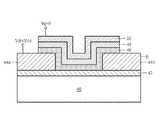
図1に示すように、基板40上に絶縁膜42が積層されている。基板40は、所定の導電性の不純物がドーピングされた半導体基板であり、例えば、n型不純物がドーピングされたシリコン基板でありうる。絶縁膜42は、例えば、熱酸化膜でありうる。絶縁膜42上に第1導電層パターン44a及び第2導電層パターン44bが存在する。第1導電層パターン44a及び第2導電層パターン44bは、所定間隔で離隔されている。第1導電層パターン44a及び第2導電層パターン44bのうち何れか一つは、ソースとして使用され、他の一つは、ドレインとして使用される。第1導電層パターン44a及び第2導電層パターン44bは、下記の物性変換層46とショットキー接合され得る金属膜またはシリサイド膜でありうる。前記金属膜としては、例えば、Al膜、Ti膜、Au膜などが使用され、前記シリサイド膜としては、例えば、PtSi膜、NiSi2膜が使用され得る。第1導電層パターン44aと第2導電層パターン44bとの間の絶縁膜42上に物性変換層46が形成されている。物性変換層46は、第1導電層パターン44a及び第2導電層パターン44bの上部面まで拡張されている。物性変換層46は、金属−半導体(絶縁体)変換物質膜であって、第1導電層パターン44aと第2導電層パターン44bとの間に印加される電圧の大きさによって金属または半導体(絶縁体)となる物質膜である。物性変換層46は、カルコゲニド物質膜、遷移金属酸化膜、または多様な遷移金属酸化物を含む合成物質膜でありうる。また、物性変換層46は、アルミニウム酸化膜またはアルミニウム酸化物を含む合成物質膜でありうる。前記遷移金属酸化膜をなす遷移金属は、例えば、Ti、V、Fe、Ni、Nb、Taでありうる。物性変換層46上に高誘電膜48が存在する。高誘電膜48は、物性変換層46と反応性が低く、超薄膜加工の可能な物質膜、例えば、Al2O3膜、HfO2膜、ZrO2膜等でありうる。高誘電膜48上にゲート電極50が存在する。As shown in FIG. 1, an
次いで、図1に示すトランジスタの動作について説明する。 Next, operation of the transistor illustrated in FIG. 1 is described.
まず、図2に示すように、ゲート電極50に印加される電圧(以下、「ゲート電圧」と称する)Vgを0Vに維持して、第1導電層パターン44aと第2導電層パターン44bとの電位差Vdを、第1導電層パターン44aと第2導電層パターン44bとの間の閾電圧Vthより低く維持する場合、第1導電層パターン44aと第2導電層パターン44bとの間の物性変換層46は、半導体あるいは絶縁体のような特性を維持する。したがって、第1導電層パターン44aと第2導電層パターン44bとの間にはチャンネルが形成されない。 First, as shown in FIG. 2, the voltage (hereinafter referred to as “gate voltage”) Vg applied to the
一方、図3に示すように、ゲート電圧Vgを0Vで維持した状態で第1導電層パターン44aと第2導電層パターン44bとの電位差Vdが閾電圧Vthより大きい場合(Vd>Vth)、第1導電層パターン44aと第2導電層パターン44bとの間の物性変換層46は金属と同じ特性を有する。これにより、第1導電層パターン44aと第2導電層パターン44bとの間にチャンネルCが形成されて、第1導電層パターン44aと第2導電層パターン44bとの間に電流が流れる。 On the other hand, as shown in FIG. 3, when the potential difference Vd between the first
一方、図4に示すように、ゲート電圧Vgが0より大きい場合、第1導電層パターン44aと第2導電層パターン44bとの間の物性変換層46で底部の近傍のホールhの密度が高まる。これにより、第1導電層パターン44aと第2導電層パターン44bとの電位差Vdが閾電圧Vthより小さくても、第1導電層パターン44aと第2導電層パターン44bとの間の物性変換層46にチャンネルC1が形成される。このような結果は、ゲート電圧Vgが0より大きいとき、第1導電層パターン44aと第2導電層パターン44bとの間の閾電圧Vthが低くなるということを意味する。 On the other hand, as shown in FIG. 4, when the gate voltage Vg is greater than 0, the density of holes h near the bottom increases in the physical
本発明者は、このような事実を確認するために、実験用のトランジスタを製作し、それを対象として、図2ないし図4に示すような印加条件でVd及びVgを印加して電流−電圧の特性を測定した。 In order to confirm such a fact, the present inventor manufactured an experimental transistor and applied Vd and Vg under the application conditions as shown in FIGS. The characteristics of were measured.
前記実験用のトランジスタで第1導電層パターン44a及び第2導電層パターン44bに該当するソース及びドレイン電極は、それぞれ30μm*30μmの面積を有するPtで形成した。また、物性変換層46は、50nmの厚さのTiAlOxで形成した。 The source and drain electrodes corresponding to the first
図5は、前記実験用のトランジスタから測定した電流−電圧の特性を示すグラフである。 FIG. 5 is a graph showing the current-voltage characteristics measured from the experimental transistor.
図5に示すように、前記実験用のトランジスタでソース電極とドレイン電極との間に流れる電流は、前記ソース電極とドレイン電極との電位差が1.6Vである時と2Vである時とに急増するということが分かる。前記ソース電極とドレイン電極との電位差、2Vは、前記実験用のトランジスタのゲート電圧Vgが0Vであるときの閾電圧(以下、「第1閾電圧」と称する)である。そして、前記ソース電極とドレイン電極との電位差、1.6Vは、前記実験用のトランジスタのゲート電極に0より大きなゲート電圧が印加されることによる低くなった閾電圧(以下、「第2閾電圧」と称する)である。したがって、前記実験用のトランジスタは、前記ソース電極とドレイン電極との電位差を、前記第1閾電圧と第2閾電圧との間の電圧、例えば、約1.8Vに維持した状態で、ゲート電極に0より大きな所定の電圧を印加すれば、オン状態になり、前記ゲート電極に0Vを印加すれば、オフ状態になるスイッチング素子として使用できる。すなわち、第1導電層パターン44aと第2導電層パターン44bとの電位差Vdを、ゲート電極に0Vが印加された状態で物性変換層46を金属層に変換するために、第1導電層パターン44aと第2導電層パターン44bとの間に印加されるトランジスタの駆動に必要な最小電位差(第2閾電圧)より小さくすることで、低電圧動作が可能となる。 As shown in FIG. 5, the current flowing between the source electrode and the drain electrode in the experimental transistor rapidly increases when the potential difference between the source electrode and the drain electrode is 1.6V and 2V. You can see that The potential difference between the source electrode and the drain electrode, 2V, is a threshold voltage (hereinafter referred to as “first threshold voltage”) when the gate voltage Vg of the experimental transistor is 0V. The potential difference of 1.6 V between the source electrode and the drain electrode is a threshold voltage (hereinafter referred to as “second threshold voltage”) that is lowered by applying a gate voltage larger than 0 to the gate electrode of the experimental transistor. "). Therefore, the experimental transistor maintains the potential difference between the source electrode and the drain electrode at a voltage between the first threshold voltage and the second threshold voltage, for example, about 1.8V, When a predetermined voltage higher than 0 is applied to the gate electrode, the switching element is turned on, and when 0 V is applied to the gate electrode, the switching element can be turned off. That is, in order to convert the potential difference Vd between the first
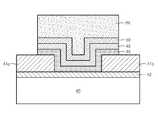
次いで、前述した本発明の実施形態によるトランジスタの製造方法を、図6ないし図8を参照して説明する。 Next, a method of manufacturing the transistor according to the above-described embodiment of the present invention will be described with reference to FIGS.
図6に示すように、基板40上に絶縁膜42を形成する。絶縁膜42上に第1導電層パターン44a及び第2導電層パターン44bを形成する。第1導電層パターン44a及び第2導電層パターン44bは、所定間隔を有して離隔されて形成する。第1導電層パターン44a及び第2導電層パターン44bは、通常の写真及びエッチング工程で形成できる。また、第1導電層パターン44a及び第2導電層パターン44bは、第1導電層パターン44aと第2導電層パターン44bとの間の絶縁膜42上に感光膜パターン(図示せず)を形成した後、第1導電層パターン44a及び第2導電層パターン44bが形成された位置に導電層を積層し、前記感光膜パターンを除去するリフトオフ(lift−off)方式で形成しても良い。基板40は、所定の導電性の不純物がドーピングされた半導体基板、例えば、n+型不純物がドーピングされたシリコン基板で形成できる。そして、絶縁膜42は、熱酸化膜、例えば、SiO2膜で形成することが望ましいが、他の絶縁膜、例えば、HfO2またはSiNxで形成しても良い。また、第1導電層パターン44a及び第2導電層パターン44bは、後続工程で形成される物性変換層とショットキー接合され得る金属膜またはシリサイド膜でありうる。前記金属膜としては、Al、Ti、Auなどが使用され、前記シリサイド膜としては、PtSi膜またはNiSi2膜が使用され得る。As shown in FIG. 6, an insulating
次いで、図7に示すように、絶縁膜42上に第1導電層パターン44a及び第2導電層パターン44bを覆う物性変換層46を形成する。物性変換層46は、第1導電層パターン44aと第2導電層パターン44bとの電位差によって、物性が金属から半導体、あるいは逆に変わる物質膜で形成できる。このような物性変換層46は、カルコゲニド物質膜または遷移金属酸化膜で形成してもよく、また複数の遷移金属酸化物を含む合成物質膜で形成しても良い。前記遷移金属酸化膜をなす遷移金属は、例えば、Ti、V、Fe、Ni、Nb、Taでありうる。また、物性変換層46は、アルミニウム酸化膜またはアルミニウム酸化物を含む合成物質膜で形成しても良い。 Next, as shown in FIG. 7, a physical
次いで、物性変換層46上に高誘電膜48とゲート電極50とを順次に形成する。高誘電膜48は、物性変換層46と反応性が低く、超薄膜加工の可能な物質膜で形成できるが、例えば、Al2O3、HfO2、ZrO2等で形成できる。次いで、ゲート電極50上に感光膜パターンPRを形成する。感光膜パターンPRは、第1導電層パターン44aと第2導電層パターン44bとの間の離隔された部分を覆い、第1導電層パターン44a及び第2導電層パターン44bの一部も覆う。このような感光膜パターンPRにより第1導電層パターン44a及び第2導電層パターン44bの露出された領域が決まる。感光膜パターンPRを形成した後、これをマスクとしてゲート電極50の露出された部分をエッチングする。前記エッチングは、第1導電層パターン44a及び第2導電層パターン44bが露出されるまで実施する。前記エッチングの結果、図8に示すように、第1導電層パターン44a及び第2導電層パターン44bが露出される。前記エッチングの後、前記感光膜パターンPRを除去すれば、図1のトランジスタが形成される。Next, a
前記の説明で多くの事項が具体的に記載されているが、それらは、発明の範囲を限定するものと言うより、望ましい実施形態の例示として解釈されねばならない。例えば、当業者ならば、物性変換層46をソース電極とドレイン電極との間にのみ形成するか、または絶縁膜42の代わりに、基板40の表面を所定の厚さほど酸化させ得るであろう。また、高誘電膜48を複数層として備え得るであろう。また、第1導電層パターン44a及び第2導電層パターン44bを、表面にシリサイド膜が形成された金属で形成できるであろう。したがって、本発明の範囲は、説明された実施形態によって決まらずに、特許請求の範囲に記載された技術的な思想によって決まらねばならない。 Although many items have been specifically described in the foregoing description, they should be construed as examples of preferred embodiments rather than limiting the scope of the invention. For example, those skilled in the art could form the physical
本発明は、トランジスタに関連した技術分野に好適に適用され得る。 The present invention can be suitably applied to a technical field related to a transistor.
40 基板、
42 絶縁膜、
44a 第1導電層パターン、
44b 第2導電層パターン、
46 物性変換層、
48 高誘電膜、
50 ゲート電極。40 substrates,
42 insulating film,
44a First conductive layer pattern,
44b second conductive layer pattern,
46 Physical property conversion layer,
48 High dielectric film,
50 Gate electrode.
Claims (23)
Translated fromJapanese前記基板上に形成された絶縁膜と、
前記絶縁膜上に離隔された第1導電層パターン及び第2導電層パターンと、
前記第1導電層パターンと第2導電層パターンとの間の前記絶縁膜上に形成された物性変換層と、
前記物性変換層上に積層された高誘電膜と、
前記高誘電膜上に形成されたゲート電極と、を備えることを特徴とするトランジスタ。A substrate,
An insulating film formed on the substrate;
A first conductive layer pattern and a second conductive layer pattern spaced apart on the insulating film;
A physical property conversion layer formed on the insulating film between the first conductive layer pattern and the second conductive layer pattern;
A high dielectric film laminated on the physical property conversion layer;
And a gate electrode formed on the high dielectric film.
前記第1導電層パターンと第2導電層パターンとの電位差を維持し、前記ゲート電極に0Vまたはこれと異なる電圧を印加することを特徴とするトランジスタの動作方法。Between the substrate, the insulating film formed on the substrate, the first conductive layer pattern and the second conductive layer pattern spaced on the insulating film, and the first conductive layer pattern and the second conductive layer pattern In a transistor operating method, comprising: a physical property conversion layer formed on the insulating film; a high dielectric film stacked on the physical property conversion layer; and a gate electrode formed on the high dielectric film.
A method for operating a transistor, wherein a potential difference between the first conductive layer pattern and the second conductive layer pattern is maintained, and a voltage of 0 V or a voltage different from the voltage is applied to the gate electrode.
前記絶縁膜上に離隔された第1導電層パターン及び第2導電層パターンを形成する第2工程と、
前記絶縁膜上に前記第1導電層パターン及び第2導電層パターンを覆う物性変換層、高誘電膜、及びゲート電極を順次に積層する第3工程と、
前記ゲート電極、前記高誘電膜及び前記物性変換層の一部を順次にエッチングして、前記第1導電層パターン及び第2導電層パターンの一部を露出させる第4工程と、を含むことを特徴とするトランジスタの製造方法。A first step of forming an insulating film on the substrate;
A second step of forming a first conductive layer pattern and a second conductive layer pattern spaced on the insulating film;
A third step of sequentially laminating a physical property conversion layer, a high dielectric film, and a gate electrode covering the first conductive layer pattern and the second conductive layer pattern on the insulating film;
A fourth step of sequentially etching a part of the gate electrode, the high dielectric film, and the physical property conversion layer to expose a part of the first conductive layer pattern and the second conductive layer pattern. A method for manufacturing a transistor.
前記絶縁膜の前記第1導電層パターン及び第2導電層パターンが形成される領域を露出させるマスクを形成する工程と、
前記絶縁膜の露出された領域上に導電層を形成する工程と、
前記マスクを除去する工程と、をさらに含むことを特徴とする請求項17に記載のトランジスタの製造方法。The second step includes
Forming a mask for exposing a region of the insulating film where the first conductive layer pattern and the second conductive layer pattern are formed;
Forming a conductive layer on the exposed region of the insulating film;
The method of manufacturing a transistor according to claim 17, further comprising: removing the mask.
Applications Claiming Priority (1)
| Application Number | Priority Date | Filing Date | Title |
|---|---|---|---|
| KR1020050017218AKR100601995B1 (en) | 2005-03-02 | 2005-03-02 | Transistor using the property conversion layer, its operation and manufacturing method |
Publications (1)
| Publication Number | Publication Date |
|---|---|
| JP2006245589Atrue JP2006245589A (en) | 2006-09-14 |
Family
ID=36943276
Family Applications (1)
| Application Number | Title | Priority Date | Filing Date |
|---|---|---|---|
| JP2006056765APendingJP2006245589A (en) | 2005-03-02 | 2006-03-02 | Transistor using physical property conversion layer, and operation and manufacturing method thereof |
Country Status (4)
| Country | Link |
|---|---|
| US (1) | US20060197082A1 (en) |
| JP (1) | JP2006245589A (en) |
| KR (1) | KR100601995B1 (en) |
| CN (1) | CN1832198A (en) |
Cited By (1)
| Publication number | Priority date | Publication date | Assignee | Title |
|---|---|---|---|---|
| US9209196B2 (en) | 2011-11-30 | 2015-12-08 | Sharp Kabushiki Kaisha | Memory circuit, method of driving the same, nonvolatile storage device using the same, and liquid crystal display device |
Families Citing this family (4)
| Publication number | Priority date | Publication date | Assignee | Title |
|---|---|---|---|---|
| US7883931B2 (en) | 2008-02-06 | 2011-02-08 | Micron Technology, Inc. | Methods of forming memory cells, and methods of forming programmed memory cells |
| KR101348059B1 (en) | 2012-07-06 | 2014-01-03 | 성균관대학교산학협력단 | Thin film transistor comprising oxygen plasma treated channel layer and method of manufacturing the same |
| US20170317141A1 (en)* | 2016-04-28 | 2017-11-02 | HGST Netherlands B.V. | Nonvolatile schottky barrier memory transistor |
| KR101900045B1 (en) | 2017-04-28 | 2018-09-18 | 연세대학교 산학협력단 | Method for manufacturing transister comprising transition metal chalcogenides channel using dielectric with high dielectric constant and transister manufactured by the same |
Family Cites Families (6)
| Publication number | Priority date | Publication date | Assignee | Title |
|---|---|---|---|---|
| KR20020002897A (en)* | 2000-06-30 | 2002-01-10 | 박종섭 | Structure and Method for manufacturing gate of FRAM |
| US6844604B2 (en) | 2001-02-02 | 2005-01-18 | Samsung Electronics Co., Ltd. | Dielectric layer for semiconductor device and method of manufacturing the same |
| US6548422B1 (en) | 2001-09-27 | 2003-04-15 | Agere Systems, Inc. | Method and structure for oxide/silicon nitride interface substructure improvements |
| JP2003332582A (en)* | 2002-05-13 | 2003-11-21 | Toshiba Corp | Semiconductor device and manufacturing method thereof |
| KR100695150B1 (en)* | 2005-05-12 | 2007-03-14 | 삼성전자주식회사 | Transistor using metal-insulator conversion material and manufacturing method thereof |
| KR100791197B1 (en)* | 2005-06-16 | 2008-01-02 | 후지쯔 가부시끼가이샤 | Method of forming dielectric film, method of manufacturing semiconductor device, and semiconductor device |
- 2005
- 2005-03-02KRKR1020050017218Apatent/KR100601995B1/ennot_activeExpired - Fee Related
- 2006
- 2006-02-28USUS11/363,235patent/US20060197082A1/ennot_activeAbandoned
- 2006-03-01CNCNA2006100198592Apatent/CN1832198A/enactivePending
- 2006-03-02JPJP2006056765Apatent/JP2006245589A/enactivePending
Cited By (1)
| Publication number | Priority date | Publication date | Assignee | Title |
|---|---|---|---|---|
| US9209196B2 (en) | 2011-11-30 | 2015-12-08 | Sharp Kabushiki Kaisha | Memory circuit, method of driving the same, nonvolatile storage device using the same, and liquid crystal display device |
Also Published As
| Publication number | Publication date |
|---|---|
| CN1832198A (en) | 2006-09-13 |
| KR100601995B1 (en) | 2006-07-18 |
| US20060197082A1 (en) | 2006-09-07 |
Similar Documents
| Publication | Publication Date | Title |
|---|---|---|
| KR100695150B1 (en) | Transistor using metal-insulator conversion material and manufacturing method thereof | |
| JP5498662B2 (en) | Semiconductor device and manufacturing method of semiconductor device | |
| KR101025846B1 (en) | Transistors in Semiconductor Devices Containing Carbon Nanotube Channels | |
| US9711613B2 (en) | Stacked graphene field-effect transistor | |
| US9825060B2 (en) | Semiconductor device | |
| US9318573B2 (en) | Field effect transistor having germanium nanorod and method of manufacturing the same | |
| TWI804302B (en) | Semiconductor device and manufacturing method thereof | |
| JP2009004787A (en) | Zn oxide thin film transistor and manufacturing method thereof, and etching solution of Zn oxide and manufacturing method thereof | |
| CN102543886B (en) | Manufacturing method of gated diode semiconductor memory device | |
| CN102569066B (en) | Manufacturing method for gate controlled diode semiconductor device | |
| JP2006245589A (en) | Transistor using physical property conversion layer, and operation and manufacturing method thereof | |
| JP2006526273A (en) | Field effect transistor using insulator-semiconductor phase change material film as channel material and method of manufacturing the same | |
| US20130178012A1 (en) | Method for manufacturing a gate-control diode semiconductor device | |
| US9653612B2 (en) | Semiconductor device | |
| TW201205810A (en) | Method of manufacturing thin film transistors and transistor circuits | |
| US20060220158A1 (en) | Semiconductor device and manufacturing method thereof | |
| KR100496432B1 (en) | Self-assembled monolayer field-effect transistors and methods of manufacturing the same | |
| JP6067638B2 (en) | Thin film transistor and manufacturing method thereof | |
| KR102824246B1 (en) | Modulation-doped high-mobility semiconductor transistors using monolithic oxidation process and its manufacturing method | |
| TWI600164B (en) | Microelectronic structure and its formation method (1) | |
| TW201513420A (en) | Organic thin film transistor |