JP2006244561A - Semiconductor apparatus - Google Patents
Semiconductor apparatusDownload PDFInfo
- Publication number
- JP2006244561A JP2006244561AJP2005056010AJP2005056010AJP2006244561AJP 2006244561 AJP2006244561 AJP 2006244561AJP 2005056010 AJP2005056010 AJP 2005056010AJP 2005056010 AJP2005056010 AJP 2005056010AJP 2006244561 AJP2006244561 AJP 2006244561A
- Authority
- JP
- Japan
- Prior art keywords
- voltage
- test
- semiconductor device
- time
- phase change
- Prior art date
- Legal status (The legal status is an assumption and is not a legal conclusion. Google has not performed a legal analysis and makes no representation as to the accuracy of the status listed.)
- Pending
Links
- 239000004065semiconductorSubstances0.000titleclaimsabstractdescription47
- 238000012360testing methodMethods0.000claimsabstractdescription119
- 239000000463materialSubstances0.000claimsabstractdescription4
- 150000004770chalcogenidesChemical class0.000claimsdescription2
- 238000002425crystallisationMethods0.000claimsdescription2
- 230000008025crystallizationEffects0.000claimsdescription2
- 230000008859changeEffects0.000abstractdescription81
- 230000014759maintenance of locationEffects0.000abstractdescription28
- 230000007704transitionEffects0.000abstractdescription3
- 238000010586diagramMethods0.000description26
- 238000000034methodMethods0.000description17
- 230000007246mechanismEffects0.000description9
- 230000006866deteriorationEffects0.000description8
- 239000002184metalSubstances0.000description6
- 230000004913activationEffects0.000description5
- 238000005516engineering processMethods0.000description5
- 101000623061Drosophila melanogaster 40S ribosomal protein S26Proteins0.000description4
- 230000006870functionEffects0.000description4
- 101000575029Bacillus subtilis (strain 168) 50S ribosomal protein L11Proteins0.000description3
- 102100035793CD83 antigenHuman genes0.000description3
- 101000946856Homo sapiens CD83 antigenProteins0.000description3
- 230000002159abnormal effectEffects0.000description3
- 230000004048modificationEffects0.000description3
- 238000012986modificationMethods0.000description3
- 239000012782phase change materialSubstances0.000description3
- 238000012216screeningMethods0.000description3
- 239000000758substrateSubstances0.000description3
- 238000011156evaluationMethods0.000description2
- 238000010438heat treatmentMethods0.000description2
- 238000002955isolationMethods0.000description2
- 230000003287optical effectEffects0.000description2
- 229910021420polycrystalline siliconInorganic materials0.000description2
- 229920005591polysiliconPolymers0.000description2
- 230000000717retained effectEffects0.000description2
- 238000010187selection methodMethods0.000description2
- 229910021332silicideInorganic materials0.000description2
- FVBUAEGBCNSCDD-UHFFFAOYSA-Nsilicide(4-)Chemical compound[Si-4]FVBUAEGBCNSCDD-UHFFFAOYSA-N0.000description2
- 230000005856abnormalityEffects0.000description1
- 230000001133accelerationEffects0.000description1
- 230000003213activating effectEffects0.000description1
- 230000000295complement effectEffects0.000description1
- 239000013078crystalSubstances0.000description1
- 230000003247decreasing effectEffects0.000description1
- 230000007547defectEffects0.000description1
- 230000002950deficientEffects0.000description1
- 238000009792diffusion processMethods0.000description1
- 230000000694effectsEffects0.000description1
- 230000005611electricityEffects0.000description1
- 230000009191jumpingEffects0.000description1
- 229910021421monocrystalline siliconInorganic materials0.000description1
- 230000008569processEffects0.000description1
- 230000003252repetitive effectEffects0.000description1
- 239000007787solidSubstances0.000description1
- 238000010998test methodMethods0.000description1
- 230000005641tunnelingEffects0.000description1
Images


Classifications
- G—PHYSICS
- G11—INFORMATION STORAGE
- G11C—STATIC STORES
- G11C29/00—Checking stores for correct operation ; Subsequent repair; Testing stores during standby or offline operation
- G11C29/04—Detection or location of defective memory elements, e.g. cell constructio details, timing of test signals
- G11C29/50—Marginal testing, e.g. race, voltage or current testing
- G11C29/50016—Marginal testing, e.g. race, voltage or current testing of retention
- G—PHYSICS
- G11—INFORMATION STORAGE
- G11C—STATIC STORES
- G11C13/00—Digital stores characterised by the use of storage elements not covered by groups G11C11/00, G11C23/00, or G11C25/00
- G11C13/0002—Digital stores characterised by the use of storage elements not covered by groups G11C11/00, G11C23/00, or G11C25/00 using resistive RAM [RRAM] elements
- G11C13/0004—Digital stores characterised by the use of storage elements not covered by groups G11C11/00, G11C23/00, or G11C25/00 using resistive RAM [RRAM] elements comprising amorphous/crystalline phase transition cells
- G—PHYSICS
- G11—INFORMATION STORAGE
- G11C—STATIC STORES
- G11C2213/00—Indexing scheme relating to G11C13/00 for features not covered by this group
- G11C2213/70—Resistive array aspects
- G11C2213/79—Array wherein the access device being a transistor
Landscapes
- For Increasing The Reliability Of Semiconductor Memories (AREA)
- Semiconductor Memories (AREA)
Abstract
Description
Translated fromJapanese本発明は、半導体装置に関し、特に相変化メモリおよびそのテスト回路を含む半導体装置に適用して有効な技術に関するものである。 The present invention relates to a semiconductor device, and more particularly to a technique effective when applied to a semiconductor device including a phase change memory and its test circuit.
本発明者が検討したところによれば、相変化材料を用いたメモリの技術に関しては、以下のようなものが考えられる。 According to a study by the present inventor, the following can be considered as a memory technology using a phase change material.
「相変化メモリ」と呼ばれる技術の開発が進んでいる。これは、書き換え可能なCDやDVDなどの光ディスクでも利用されている相変化膜、相変化素子を記憶素子に使う技術で、相変化素子がアモルファス状態にあるか、結晶状態にあるかで、‘0’と‘1’を記憶する。光ディスクでは、高い出力のレーザーで局所的に加熱し、アモルファス状態や結晶状態を作ることで書き込みを行う。 A technology called “phase change memory” is being developed. This is a technology that uses phase change films and phase change elements that are also used in rewritable optical discs such as CDs and DVDs as storage elements. Whether the phase change elements are in an amorphous state or a crystalline state, Memorize “0” and “1”. In optical disks, writing is performed by locally heating with a high-power laser to create an amorphous state or a crystalline state.
一方、相変化メモリでは、書込みは電流パルスを用いて局所的に加熱することで行い、読出しは状態の変化による電気抵抗値の変化を検出して行う。これを実現するために、非特許文献1に記載されているように、トランジスタの出力にヒータ部分を設けてここに相変化素子を接続し、他方にも金属を接続し電流が流れるようにする。このようにすれば、トランジスタで選択された部分にのみ電流を流すことができる。 On the other hand, in the phase change memory, writing is performed by locally heating using a current pulse, and reading is performed by detecting a change in electrical resistance value due to a change in state. In order to realize this, as described in Non-Patent
書き換え動作は、リセットと呼ばれる、一旦相変化素子に大電流を流して加熱し溶解させ、その後電流を切って、急冷させる動作(アモルファス状態となり、電気的には抵抗が高い)、及び、この電流よりは小さな電流を一定時間流し続け、その間の熱で相変化素子を結晶化させるセット動作(結晶化状態では電気的には抵抗が低い)とからなる。読出しは、トランジスタをオンさせて、この時の相変化素子の抵抗の大小をこのトランジスタに流れる電流で読み取る。
ところで、前記のような相変化材料を用いたメモリのテスト技術について、本発明者が検討した結果、以下のようなことが明らかとなった。 By the way, as a result of the study of the memory testing technique using the phase change material as described above, the following has been clarified.
このような相変化メモリでは、初期不良をスクリーニングするテスト手法の開発が必須である。特に、相変化メモリのような不揮発メモリでは、保持したデータを例えば10年間保持できるか否かが重要な事項であるが、これを高速にテストする必要がある。 In such a phase change memory, it is essential to develop a test method for screening initial defects. In particular, in a non-volatile memory such as a phase change memory, whether or not the retained data can be retained for, for example, 10 years is an important matter, and this needs to be tested at a high speed.
この検討にあたり、本発明者は、相変化メモリにおいては、読出し時などでの劣化の機構と、相変化素子を放置した時の劣化の機構とが同じであることを見出した。ここで、この劣化の機構に関し、例えば代表的な不揮発メモリであるフラッシュメモリと比較して説明する。 In this examination, the present inventor has found that in the phase change memory, the deterioration mechanism at the time of reading and the like is the same as the deterioration mechanism when the phase change element is left unattended. Here, this deterioration mechanism will be described in comparison with, for example, a flash memory which is a typical nonvolatile memory.
図15は、本発明が立脚する相変化メモリ素子の特性の一例を示す図である。この図では、横軸は、絶対温度Tとボルツマン定数kの積の逆数であり、縦軸はリテンション時間である。リテンションとは、ある温度、素子の記憶情報が保たれる時間である。相変化メモリのような不揮発メモリでは、リテンション時間が重要な評価項目となる。このグラフに、正常な相変化メモリ素子の特性をプロットすると、S1の線とS3の線との間であるS2の線となる。ここでは、S2は一本しか示していないが、これは、S1の線とS3の線との間の任意の線を表し、S1の線とS3の線とがばらつきの上限と下限とを示している。この線の中にあれば、温度T2において、所望のリテンション時間t2を達成することができる。 FIG. 15 is a diagram illustrating an example of characteristics of a phase change memory element on which the present invention is based. In this figure, the horizontal axis is the reciprocal of the product of the absolute temperature T and the Boltzmann constant k, and the vertical axis is the retention time. Retention is a time at which memory information of an element is kept at a certain temperature. In a nonvolatile memory such as a phase change memory, retention time is an important evaluation item. When the characteristics of a normal phase change memory element are plotted on this graph, a line S2 between the line S1 and the line S3 is obtained. Here, only one S2 is shown, but this represents an arbitrary line between the S1 line and the S3 line, and the S1 line and the S3 line indicate the upper and lower limits of variation. ing. If it is in this line, the desired retention time t2 can be achieved at the temperature T2.
しかしながら、異常な相変化メモリ素子は、この領域とは外れてしまう。例えば、S4やS5の線の特性となってしまうのである。この素子では、もはや温度がT2の時に、所望のリテンション時間であるt2を達成できないのである。ここで相変化素子特有の性質を用いることになる。 However, the abnormal phase change memory element is out of this region. For example, it becomes the characteristic of the line of S4 and S5. With this device, the desired retention time t2 can no longer be achieved when the temperature is T2. Here, the characteristics peculiar to the phase change element are used.
すなわち、相変化素子では、例えば、通常の読出しなどを行う際にも熱が発生してメモリセル素子の温度が上昇する。これは、この図15で温度を上げた時のリテンション特性を見ているのと同じである。そうすると、図15のひとつの同じ線の上で温度を上げることによりリテンション時間が短くなる。つまり、読出しとはディスターブを与えることであるが、これはこのリテンションの特性を加速して見ていることにもなる。 That is, in the phase change element, for example, heat is generated even during normal reading and the temperature of the memory cell element rises. This is the same as viewing the retention characteristics when the temperature is raised in FIG. Then, the retention time is shortened by raising the temperature on one and the same line in FIG. In other words, reading is to give disturbance, but this also means that the retention characteristic is accelerated.
ディスターブとリテンションとが同じ特性に立脚していることは相変化素子の大きな特徴である。もっと電圧を上げれば、もっと加速する。或いは、長く時間をかける(ディスターブ時間を長くする)ことによって、このリテンション特性を再現することができる。相変化メモリのような不揮発メモリでは、リテンション時間が重要な評価項目であり、これの良否を判断するのがテストでのスクリーニングの主な目的である。 The fact that disturb and retention are based on the same characteristics is a major feature of phase change elements. The more you increase the voltage, the more you accelerate. Alternatively, this retention characteristic can be reproduced by taking a long time (extending the disturb time). In a nonvolatile memory such as a phase change memory, the retention time is an important evaluation item, and the main purpose of screening in a test is to determine whether it is good or bad.
本発明では、本発明者等が見出した“相変化素子では、リテンション特性とディスターブ特性が同じ機構に立脚すること”を利用する。すなわち、テストではメモリ素子に少し大きな電流を流すことで温度を上げて、このメモリ素子の劣化の具合を見るのである。例えば、温度T1を与えたとする。すると、正常なS1、S2、S3の中にあれば、t1の時間を経過した際にも素子は正常な記憶情報を保持している。しかし、もし、異常な性質であるS4やS5のような相変化素子であれば、t1の時間では正常な記憶情報を保持できないのである。これによって、異常な素子を取り除いたり、或いは、この結果を元に、異常が起こり難い条件を見出すことができるのである。 In the present invention, “the phase change element is based on the same mechanism of the retention characteristic and the disturb characteristic” found by the present inventors is utilized. That is, in the test, the temperature is raised by passing a little large current through the memory element to see how the memory element deteriorates. For example, assume that a temperature T1 is given. Then, if it is in normal S1, S2, S3, the element holds normal storage information even after the time t1 has elapsed. However, if it is a phase change element such as S4 or S5 having an abnormal property, normal stored information cannot be held at the time t1. As a result, abnormal elements can be removed, or conditions on which abnormalities are unlikely to occur can be found based on the results.
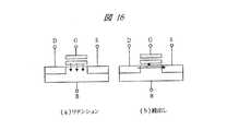
一方、フラッシュメモリにおける劣化の機構は次のようになる。図16は、フラッシュメモリにおける劣化の機構を説明するための図であり、(a)は情報保持状態(リテンション)の模式図、(b)は読出し状態の模式図を示すものである。フラッシュメモリでは、この2つでは異なる物理機構が支配している。すなわち、リテンションでは、図16(a)に示すように、フローティングゲートの中の電子が熱によって励起され、絶縁膜をトンネリングして抜け出てしまうことにより劣化が発生する。この特性は温度が高いほどおこりやすく、例えば、図15と同様な性質を持つ。 On the other hand, the deterioration mechanism in the flash memory is as follows. FIGS. 16A and 16B are diagrams for explaining a mechanism of deterioration in the flash memory. FIG. 16A is a schematic diagram of an information holding state (retention), and FIG. 16B is a schematic diagram of a reading state. In the flash memory, these two dominate different physical mechanisms. That is, in the retention, as shown in FIG. 16 (a), electrons in the floating gate are excited by heat and tunnel through the insulating film to cause deterioration. This characteristic is more likely to occur as the temperature is higher, and has, for example, the same properties as in FIG.
一方、ディスターブでは、図16(b)のような読出しの際に、ドレインからソースに流れる電流の一部が、高いエネルギーを持ち、フローティングゲートに飛び込むことによって書かれている情報が変わってしまうことにより劣化が発生する。これは、電圧には大きく依存するが、温度の依存性がリテンションを決めているトンネリング程大きくはない。 On the other hand, in the disturb mode, when reading as shown in FIG. 16B, a part of the current flowing from the drain to the source has high energy, and the written information is changed by jumping into the floating gate. Causes deterioration. This depends largely on the voltage, but not as much as the tunneling where the temperature dependence determines the retention.
ここで、テストに話を戻すと、2つの物理機構が存在するということは、2通りのテストを行なう必要があるということである。このため、フラッシュメモリでは、リテンションの試験と、ディスターブの試験とは、一般に異なる温度で別々に行なわれる。これは、フラッシュメモリのテスト時間を増大させている。 Here, returning to the test, the existence of two physical mechanisms means that two kinds of tests need to be performed. For this reason, in the flash memory, the retention test and the disturb test are generally performed separately at different temperatures. This increases the test time of the flash memory.
これと異なり、相変化メモリでは、前述したように、電圧を少し高くするか、または時間を少し長くして、通常の読出しと同じ動作を行なえば、リテンション特性とディスターブ特性、両方を同時に試験することができるのである。そこで、本発明の目的は、この特性を利用することで、テスト機能に関する回路素子増加を最小に抑え、テストの容易化を実現可能な半導体装置を提供することにある。また、テスト時間の短縮を実現可能な半導体装置を提供することにある。 In contrast, in the phase change memory, as described above, if the same operation as normal reading is performed with a slightly higher voltage or a slightly longer time, both the retention characteristic and the disturb characteristic are tested simultaneously. It can be done. SUMMARY OF THE INVENTION An object of the present invention is to provide a semiconductor device capable of minimizing an increase in circuit elements relating to a test function and facilitating a test by utilizing this characteristic. Another object of the present invention is to provide a semiconductor device that can reduce the test time.
本発明の前記ならびにその他の目的と新規な特徴は、本明細書の記述および添付図面から明らかになるであろう。 The above and other objects and novel features of the present invention will be apparent from the description of this specification and the accompanying drawings.
本願において開示される発明のうち、代表的なものの概要を簡単に説明すれば、次のとおりである。 Of the inventions disclosed in the present application, the outline of typical ones will be briefly described as follows.
本発明の半導体装置は、メモリ素子を結晶化状態にする際(セット動作時)にメモリ素子に印加する電圧またはそのタイミングと、メモリ素子の読出し動作を行う際にメモリ素子に印加する電圧またはそのタイミングとを組み合わせて利用することでテスト動作を行う回路を備えたものである。ここで、テスト動作とは、所謂リテンション試験を意味するが、同時にディスターブ試験とすることも可能である。すなわち、リテンション試験を行うことでディスターブ試験を兼ね備えることもでき、テスト時間の短縮が図れる。 The semiconductor device of the present invention has a voltage applied to the memory element when the memory element is crystallized (during a set operation) or a timing thereof, and a voltage applied to the memory element when a read operation of the memory element is performed or the voltage applied thereto. A circuit for performing a test operation by using a combination with timing is provided. Here, the test operation means a so-called retention test, but can also be a disturb test at the same time. That is, by performing a retention test, a disturb test can also be provided, and the test time can be shortened.
テスト動作時の具体的な電圧およびタイミングとしては、例えば、セット動作時の電圧を読出し動作時のタイミングでメモリ素子に印加する方式が挙げられる。この場合、電圧発生回路およびタイミング発生回路を本来備えている回路で共有することができるため、小面積化が可能となる。そして、これによって、正常なメモリ素子に対してセット動作が行われない範囲内で、電圧ベースで加速したリテンション試験を容易に行うことが可能となる。 Specific examples of the voltage and timing at the time of the test operation include a method in which the voltage at the time of the set operation is applied to the memory element at the timing at the time of the read operation. In this case, since the voltage generation circuit and the timing generation circuit can be shared by the originally provided circuit, the area can be reduced. This makes it possible to easily perform a voltage-based accelerated retention test within a range where a normal memory element is not set.
また、この方式に対して、電圧またはタイミングの一方を本来備えている回路で共有して生成し、他方を別途設けた回路で生成することも可能である。電圧を別回路で生成する場合、その電圧は、読出し動作時の電圧よりも高くセット動作時の電圧よりも低くするとよい。また、タイミングを別回路で生成する場合、セット動作時のタイミングよりも短くする必要がある。これらの場合も、その電圧またはタイミングを生成する際に本来備えている回路の一部を共有できるため、小面積化を実現できる。そして、正常なメモリ素子に対してセット動作が行われない範囲内で、電圧ベースまたは電圧印加時間ベースで加速したリテンション試験を容易に行うことが可能となる。 In addition, for this method, it is also possible to generate a voltage or timing by sharing it with a circuit originally provided, and generate the other with a circuit provided separately. When the voltage is generated by another circuit, the voltage is preferably higher than the voltage during the read operation and lower than the voltage during the set operation. Further, when the timing is generated by another circuit, it is necessary to make the timing shorter than the timing at the time of the set operation. In these cases as well, a part of the circuit originally provided for generating the voltage or timing can be shared, so that the area can be reduced. In addition, it is possible to easily perform a retention test accelerated on a voltage basis or a voltage application time basis within a range where a set operation is not performed on a normal memory element.
また更に、テスト動作時の具体的な電圧およびタイミングの別の例としては、読出し動作時の電圧をセット動作時のタイミングでメモリ素子に印加する方式が挙げられる。この場合、前述した説明と同様に小面積が可能となり、電圧印加時間ベースで加速したリテンション試験を容易に行うことが可能となる。 Furthermore, another example of the specific voltage and timing at the time of the test operation is a method in which the voltage at the time of the read operation is applied to the memory element at the timing at the time of the set operation. In this case, a small area is possible as described above, and a retention test accelerated on a voltage application time basis can be easily performed.
なお、これらは、メモリ素子にカルコゲナイド材料を含む相変化メモリ備えた半導体装置に適用して特に有益なものとなる。 These are particularly useful when applied to a semiconductor device including a phase change memory including a chalcogenide material in a memory element.
本願において開示される発明のうち、代表的なものによって得られる効果を簡単に説明すれば、特に相変化メモリを含む半導体装置において、テストの容易化が実現可能となる。また、テスト時間の短縮が実現可能となる。 If the effects obtained by typical ones of the inventions disclosed in the present application are briefly described, it is possible to facilitate the test particularly in a semiconductor device including a phase change memory. In addition, the test time can be shortened.
以下、本発明の実施の形態を図面に基づいて詳細に説明する。なお、実施の形態を説明するための全図において、同一の部材には原則として同一の符号を付し、その繰り返しの説明は省略する。また、実施の形態の各機能ブロックを構成する回路素子は、特に制限されないが、公知のCMOS(相補型MOSトランジスタ)等の集積回路技術によって、単結晶シリコンのような半導体基板上に形成される。 Hereinafter, embodiments of the present invention will be described in detail with reference to the drawings. Note that components having the same function are denoted by the same reference symbols throughout the drawings for describing the embodiment, and the repetitive description thereof will be omitted. The circuit elements constituting each functional block of the embodiment are not particularly limited, but are formed on a semiconductor substrate such as single crystal silicon by a known integrated circuit technology such as a CMOS (complementary MOS transistor). .
なお、図面において、PMOSトランジスタにはゲートに丸印の記号を付すことで、NMOSトランジスタと区別することとする。図面にはMOSトランジスタの基板電位の接続は特に明記していないが、MOSトランジスタが正常動作可能な範囲であれば、その接続方法は特に限定しない。 In the drawing, the PMOS transistor is distinguished from the NMOS transistor by adding a circle symbol to the gate. Although the connection of the substrate potential of the MOS transistor is not particularly specified in the drawing, the connection method is not particularly limited as long as the MOS transistor can operate normally.
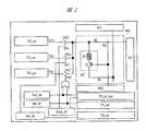
図1は、本発明の一実施の形態による半導体装置において、その構成の一例を示すブロック図である。図1において特徴的なことは、セット用ビット線電圧電源VG_setをセット動作とテスト動作の両方に使用すること、そのための方法、機能を有することと、読出し動作とテスト動作のタイミング発生回路がその多くを共用し読出し/テスト時タイミング発生回路TG_rd_testとしている点である。このようにすることで、前述したように相変化メモリに用いる材料の特性に合った有効なテスト動作を行えることを発明者は見出しており、これに着目することにより回路増加を小さく抑えることが可能となる。 FIG. 1 is a block diagram showing an example of the configuration of a semiconductor device according to an embodiment of the present invention. 1 is characterized in that the set bit line voltage power supply VG_set is used for both the set operation and the test operation, has a method and a function therefor, and a timing generation circuit for the read operation and the test operation includes A common point is that the read / test timing generation circuit TG_rd_test is shared. By doing so, the inventor has found that an effective test operation can be performed in accordance with the characteristics of the material used for the phase change memory as described above. It becomes possible.
以下、詳しく述べれば、メモリアレーMAでは、ここではひとつしか示していないメモリセルMCが2次元に敷き詰められており、各メモリセルMCは、トランジスタM1と相変化素子P1とで成っており、ビット線BLとワード線WLとソース線SLとの電圧関係でこのメモリセルMCが選択できるようになっている。ソースドライバSDは、ソース線SLを駆動する回路であり、ワードドライバWDは、ワード線WLを駆動する回路であり、センスアンプSAは、ビット線BLに現れた信号電圧を増幅する回路である。 More specifically, in the memory array MA, only one memory cell MC, which is shown here, is laid out in two dimensions, and each memory cell MC is composed of a transistor M1 and a phase change element P1, This memory cell MC can be selected by the voltage relationship among the line BL, the word line WL, and the source line SL. The source driver SD is a circuit that drives the source line SL, the word driver WD is a circuit that drives the word line WL, and the sense amplifier SA is a circuit that amplifies the signal voltage that appears on the bit line BL.
相変化メモリでは、セット動作とリセット動作と読出し動作と、テスト動作を行うが、それぞれの動作を行うために、セット制御回路Set_ctl、リセット制御回路Rst_ctl、読出し制御回路Read_ctl、及びテスト制御回路Test_ctlが必要であり、これによって各々の動作に必要な時間間隔や動作開始の信号などのタイミングが、セット時タイミング発生回路TG_set、リセット時タイミング発生回路TG_rst、読出し/テスト時タイミング発生回路TG_rd_testで発生させられる。この時、前述のように本発明では、読出し/テスト時タイミング発生回路TG_rd_testとして、読出し動作とテスト動作のタイミングの多くを共用し、回路もまた多くを共用していることが特徴である。なお、通常動作からテスト動作への遷移は、外部からのコマンド入力又はテスト端子からの入力により行われる。 In the phase change memory, a set operation, a reset operation, a read operation, and a test operation are performed. In order to perform the respective operations, a set control circuit Set_ctl, a reset control circuit Rst_ctl, a read control circuit Read_ctl, and a test control circuit Test_ctl are included. As a result, timing such as a time interval and an operation start signal required for each operation is generated by the set timing generation circuit TG_set, the reset timing generation circuit TG_rst, and the read / test timing generation circuit TG_rd_test. . At this time, as described above, the present invention is characterized in that as the read / test timing generation circuit TG_rd_test, most of the timings of the read operation and the test operation are shared and many of the circuits are also shared. The transition from the normal operation to the test operation is performed by an external command input or an input from a test terminal.
また、相変化メモリでは複数の電圧を用いるが、この実施の形態では、セット動作とリセット動作と読出し動作とテスト動作に際し、ビット線BLの電圧を切り換えて相変化素子P1に印加される電圧を変えている例を示している。すなわち、セット用ビット線電圧電源VG_set(VS1を発生)、リセット用ビット線電圧電源VG_rst(VR1を発生)、読出しビット線電圧電源VG_rd(VY1を発生)を持つ。一般に、これらの発生電圧の大小関係は、VR1>VS1>VY1である。 The phase change memory uses a plurality of voltages. In this embodiment, the voltage applied to the phase change element P1 by switching the voltage of the bit line BL during the set operation, the reset operation, the read operation, and the test operation. An example of changing is shown. That is, it has a set bit line voltage power supply VG_set (generates VS1), a reset bit line voltage power supply VG_rst (generates VR1), and a read bit line voltage power supply VG_rd (generates VY1). In general, the magnitude relationship between these generated voltages is VR1> VS1> VY1.
この理由は、相変化素子の書き換えが与える熱の大きさによるためであり、リセット動作時にはVR1で大きな熱を与え(そして急速に取り去り)、セット動作時にはこれより小さな熱を与える。一方、読出しは、できるだけ与える熱が小さい方が好ましいので電圧は低くなる。読出し時に与える熱が小さいのが好ましいのは、この熱によって相変化の状態が変化する、いわゆるディスターブを与えることを最小にするためである。なお、ある環境にこの相変化素子を放置しておくと、相変化素子は、安定な状態にたどりつく。書き換えた状態からこの状態まで変化するのに必要な時間をリテンション時間(実際上は、電気的には最初の抵抗状態から、指定した抵抗値へ変化するのに要する時間)と呼ぶ。 This is due to the amount of heat given by rewriting of the phase change element. VR1 gives a large amount of heat (and is quickly removed) during the reset operation, and gives a smaller amount of heat during the set operation. On the other hand, in reading, it is preferable that the heat applied is as small as possible, so the voltage is low. It is preferable that the heat given at the time of reading is small in order to minimize giving a so-called disturbance in which the state of the phase change is changed by this heat. If this phase change element is left in a certain environment, the phase change element reaches a stable state. The time required to change from the rewritten state to this state is referred to as retention time (in practice, the time required to change from the first resistance state to the designated resistance value in terms of electricity).
ここでの本実施例の特徴は、テスト用には別個の電源を用意せず、ディスターブ試験やリテンション試験を行う場合に、通常の読み出しビット線で電圧電源VG_rdではなく、セット用ビット線電圧電源VG_setを用いることである。これによって、通常の読み出し動作の電圧よりも高めの電圧設定を用いて加速試験を行うことが可能になる。そして、相変化のテスト動作に必要な電源電圧とタイミングとを、セット動作とリセット動作と読出し動作に必要な電圧とタイミングとから作り出すことができる。 The feature of the present embodiment is that a separate power supply is not prepared for the test, and when performing a disturb test or a retention test, a normal bit line power supply is not a voltage power supply VG_rd but a set bit line voltage power supply. VG_set is used. As a result, the acceleration test can be performed using a voltage setting higher than the voltage of the normal read operation. The power supply voltage and timing required for the phase change test operation can be generated from the voltage and timing required for the set operation, the reset operation, and the read operation.
以上のように、読出し動作用のタイミングと、セット動作用の電圧とを利用してテスト動作を行うことによって、素子数の増加を抑えチップ面積の増加を抑えて、容易にテスト動作を行うことが可能となる。また、ディスターブ試験とリテンション試験とを同時に行えるため、テスト時間の短縮が実現可能となる。 As described above, by performing the test operation using the timing for the read operation and the voltage for the set operation, the test operation can be easily performed while suppressing the increase in the number of elements and the increase in the chip area. Is possible. In addition, since the disturb test and the retention test can be performed at the same time, the test time can be shortened.
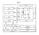
図2は、本発明の一実施の形態による半導体装置において、図1とは別の構成の一例を示すブロック図である。図2において特徴的なことは、バイポーラトランジスタQ1を用いたメモリセルMCを用いていることである。これによって、バイポーラトランジスタQ1を作成するプロセス、セル構造の場合、一般にMOSトランジスタを用いる場合と比較して大電流を流せることが期待されるが、この時のテスト動作を素子数の増加を抑えチップ面積の増加を抑えて容易に行なうことができる。 FIG. 2 is a block diagram showing an example of a configuration different from FIG. 1 in the semiconductor device according to the embodiment of the present invention. 2 is characterized in that a memory cell MC using a bipolar transistor Q1 is used. As a result, in the case of the process of creating the bipolar transistor Q1 and the cell structure, it is generally expected that a larger current can be flowed than in the case of using the MOS transistor. This can be easily performed while suppressing an increase in area.
ここでは、pnp型のバイポーラトランジスタの例で記載してある。このバイポーラトランジスタQ1のエミッタ端子とビット線BLとの間に相変化素子P1を挿入してある。他の構成は図1と同じであり、相変化のテスト動作に必要な電源電圧とタイミングとを、セット動作とリセット動作と読出し動作に必要な電圧とタイミングとから作り出すことができることが特徴である。 Here, an example of a pnp bipolar transistor is described. Phase change element P1 is inserted between the emitter terminal of bipolar transistor Q1 and bit line BL. The other configuration is the same as that of FIG. 1, and is characterized in that the power supply voltage and timing required for the phase change test operation can be generated from the voltage and timing required for the set operation, the reset operation, and the read operation. .
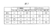
図3は、図1および図2の構成を用いたテスト動作において、ビット線電圧とタイミング発生を、通常の読出し動作、セット動作、リセット動作と共用する方法を示す表である。読出し動作では、読出し用のビット線電圧と読出し用のタイミングパルスを用いる。セット動作では、セット用のビット線電圧とセット用のタイミングパルスを用いる。更に、リセット動作では、リセット用のビット線電圧とリセット用のタイミングパルスを用いる。 FIG. 3 is a table showing a method of sharing the bit line voltage and timing generation with the normal read operation, set operation, and reset operation in the test operation using the configuration of FIGS. In the read operation, a read bit line voltage and a read timing pulse are used. In the set operation, a set bit line voltage and a set timing pulse are used. Further, in the reset operation, a reset bit line voltage and a reset timing pulse are used.
一方、本実施例のテスト動作では、これらの通常動作のビット線電圧とタイミングパルスの一部を利用する。すなわち、テスト動作においては、セット用のビット線電圧と、読出し用のタイミングパルスを用いる。このようにすることで、素子数の増加を抑えチップ面積の増加を抑えてテスト動作を容易に行うことができる。また、テスト時間の短縮が可能となる。 On the other hand, in the test operation of this embodiment, the bit line voltage and a part of the timing pulse of these normal operations are used. That is, in the test operation, a set bit line voltage and a read timing pulse are used. By doing so, it is possible to easily perform a test operation while suppressing an increase in the number of elements and an increase in chip area. In addition, the test time can be shortened.
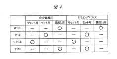
図4は、図3を変形した、ビット線電圧とタイミング発生の共有方法を示す表である。すなわち、読出し用のビット線電圧と、セット用のタイミングパルスとを用いるのである。これに伴い、電源では、読出し用のビット線電圧をテスト動作でも使用する。このような選択の方法が必要であるが、これは図1に示した方法の類推から容易であり、読出し制御回路Read_ctlとテスト制御回路Test_ctlとから、読出しビット線電圧電源VG_rdとビット線BLとを接続するスイッチSW1を制御し、両方で共用できるようにすれば良い。また、テスト動作時のタイミングの発生は、図1の読出しでは無く、セット時タイミング発生回路TG_setとその多くを兼ねれば良い。 FIG. 4 is a table showing a method of sharing the bit line voltage and timing generation, which is a modification of FIG. That is, a read bit line voltage and a set timing pulse are used. Accordingly, the power supply uses the read bit line voltage in the test operation. Such a selection method is necessary, but this is easy from the analogy of the method shown in FIG. 1, and from the read control circuit Read_ctl and the test control circuit Test_ctl, the read bit line voltage power supply VG_rd and the bit line BL It is only necessary to control the switch SW1 that connects the two so that both can be shared. In addition, the generation of the timing during the test operation is not limited to the reading shown in FIG. 1, but may be combined with the set timing generation circuit TG_set.
このようにしても、本発明の本質を変えることなく、通常よりも長い時間電圧を印加して加速試験を行うことが可能になる。そして、テストのための素子数の増加を抑えチップ面積の増加を抑えて容易にテスト動作を行うことができる。また、テスト時間の短縮が可能となる。 Even in this case, it is possible to perform an accelerated test by applying a voltage for a longer time than usual without changing the essence of the present invention. Then, it is possible to easily perform a test operation while suppressing an increase in the number of elements for testing and suppressing an increase in chip area. In addition, the test time can be shortened.
図5は、図3に対応する動作の一例を示す波形図であり、(a)、(b)、(c)、(d)は、それぞれ、リセット動作、セット動作、読出し動作、及びテスト動作を示すものである。図5において、横軸は時間軸tであり、縦軸はその時に印加されるビット線電圧Vを示している。特徴的な時間を示す記号として、t1、t2、t3があるが、t1はリセット動作の時に電圧VR1から0へ電圧を下げる時間、t2はセット動作時に一定の電圧VS1に保つ時間、t3は、読出しの時に、読出し用電圧VY1に保つ時間である。これらの電圧は、ビット線BL又はワード線WLによって選択されるメモリセルMCのビット線BLに印加される電圧を示している。 FIG. 5 is a waveform diagram showing an example of an operation corresponding to FIG. 3, and (a), (b), (c), and (d) are respectively a reset operation, a set operation, a read operation, and a test operation. Is shown. In FIG. 5, the horizontal axis is the time axis t, and the vertical axis indicates the bit line voltage V applied at that time. Symbols indicating characteristic times include t1, t2, and t3, where t1 is a time to decrease the voltage from the voltage VR1 to 0 during the reset operation, t2 is a time during which the constant voltage VS1 is maintained during the set operation, and t3 is This is the time during which reading is held at the reading voltage VY1. These voltages indicate voltages applied to the bit line BL of the memory cell MC selected by the bit line BL or the word line WL.
以上のリセット動作、セット動作、読出し動作で用いる特徴的な電圧と時間の内、本実施例では、図5(d)のテスト動作において、セット用電圧VS1と読出し用の時間t3を用いることが特徴である。この時、セット用電圧VS1は、読出し用の時間t3に通常対応する電圧VY1よりも高いことが重要である。これによって、テスト状態では、時間は読出し時と同じt3であるが、印加電圧がVY1よりの高いVS1であるので、読出し動作よりも多くのストレスをメモリセルすなわち相変化素子に与えることができるのである。 Of the characteristic voltages and times used in the above reset operation, set operation, and read operation, in this embodiment, the set voltage VS1 and the read time t3 are used in the test operation of FIG. It is a feature. At this time, it is important that the set voltage VS1 is higher than the voltage VY1 that normally corresponds to the read time t3. Thus, in the test state, the time is the same as t3 at the time of reading, but since the applied voltage is VS1 higher than VY1, more stress can be applied to the memory cell, that is, the phase change element than in the reading operation. is there.
図6は、図4に対応する動作の一例を示す波形図であり、(a)、(b)、(c)、(d)は、それぞれ、リセット動作、セット動作、読出し動作、及びテスト動作を示すものである。図6でも図5と同様にリセット動作、セット動作、読出し動作時の特徴的な電圧と時間の一部を利用してテスト動作を行なう。また、図5と同様にt1はリセット動作の時に電圧VR1から0へ電圧を下げる時間、t2はセット動作時に一定の電圧VS1に保つ時間、t3は、読出しの時に、読出し用電圧VY1に保つ時間である。 FIG. 6 is a waveform diagram showing an example of the operation corresponding to FIG. 4, and (a), (b), (c), and (d) are respectively a reset operation, a set operation, a read operation, and a test operation. Is shown. In FIG. 6, similarly to FIG. 5, the test operation is performed using a part of characteristic voltage and time during the reset operation, the set operation, and the read operation. Similarly to FIG. 5, t1 is a time for decreasing the voltage VR1 to 0 during the reset operation, t2 is a time during which the constant voltage VS1 is maintained during the set operation, and t3 is a time during which the read voltage VY1 is maintained during reading. It is.
図6の例では、図5と異なり、テスト動作においては、読出し用電圧VY1と、セット用の印加時間t2を用いる。この時、セット用の印加時間t2は、読出し用電圧VY1に通常対応する読出し動作の印加時間t3よりも長いことが重要である。これによって、テスト状態では、印加電圧は読出し時と同じVY1であるが、時間は読出し動作よりも長いセット動作時と同じt2であるため、読出し動作よりも多くのストレスをメモリセルすなわち相変化素子に与えることができるのである。 In the example of FIG. 6, unlike FIG. 5, in the test operation, the reading voltage VY1 and the setting application time t2 are used. At this time, it is important that the set application time t2 is longer than the read operation application time t3 that normally corresponds to the read voltage VY1. As a result, in the test state, the applied voltage is the same VY1 as that at the time of reading, but the time is t2 that is the same as that at the time of the setting operation longer than the reading operation. Can be given to.
図7は、本発明の一実施の形態による半導体装置において、図1とは更に別の構成の一例を示すブロック図である。本発明では、リセット動作、セット動作、読出し動作に必要な回路の一部をテストに利用し、素子数増加、面積増加を小さく抑えることが目的である。そこで、図7に示すように、図1等の読出し/テスト時タイミング発生回路TG_rd_testを読出し時のみに用いる読出し時タイミング発生回路TG_rdとし、テスト時タイミング発生回路TG_testを別途設ける。このテスト時タイミング発生回路TG_testを用いることで、テスト時の時間設定の自由度を増しつつ、かつ、電源回路はセット用の電源VG_setを用いることで回路規模を抑えることも可能である。 FIG. 7 is a block diagram showing an example of a configuration different from FIG. 1 in the semiconductor device according to the embodiment of the present invention. An object of the present invention is to use a part of a circuit necessary for a reset operation, a set operation, and a read operation for a test, and to suppress an increase in the number of elements and an area increase. Therefore, as shown in FIG. 7, the read / test timing generation circuit TG_rd_test shown in FIG. 1 or the like is used as a read timing generation circuit TG_rd used only for reading, and a test timing generation circuit TG_test is separately provided. By using the test timing generation circuit TG_test, it is possible to increase the degree of freedom of time setting at the time of the test, and it is possible to reduce the circuit scale of the power supply circuit by using the set power supply VG_set.
この実施の形態によれば、相変化素子の特性に合わせて、最適なテスト時間を選ぶことができ、目的に合ったスクリーニングを行なうことができる。これは、また、このテスト専用のタイミング発生回路を用いる場合と、他の例えば読出し時のタイミング発生回路を用いる場合とを選択する構成にすることも可能であり、相変化素子の特性により広く合致させることが可能となる。 According to this embodiment, an optimum test time can be selected in accordance with the characteristics of the phase change element, and screening suitable for the purpose can be performed. In addition, it is possible to select a case where the timing generation circuit dedicated to this test is used and another case where the timing generation circuit is used at the time of reading, for example, and widely matches the characteristics of the phase change element. It becomes possible to make it.
図8は、本発明の一実施の形態による半導体装置において、図1とは更に別の構成の一例を示すブロック図である。この例では、テスト時のタイミングは、読出しとテストとで兼ねた回路を用いるが、テスト時の電圧は、専用のテスト用ビット線電圧電源VG_test(発生電圧はVT1)を用意し、これを制御端子DS4で制御されるスイッチSW4でメモリアレーに印加する。 FIG. 8 is a block diagram showing an example of a configuration different from that of FIG. 1 in the semiconductor device according to the embodiment of the present invention. In this example, the circuit used for both reading and testing is used for the timing at the time of the test. As the voltage at the time of the test, a dedicated test bit line voltage power supply VG_test (the generated voltage is VT1) is prepared and controlled. The voltage is applied to the memory array by the switch SW4 controlled by the terminal DS4.
このようにすることで、相変化素子の特性に合った電圧をテスト動作時に印加することができるため、テストの高効率化を図ることができる。一般に、これらの発生電圧の大小関係は、VR1>VS1>VT1>VY1である。なお、テスト用ビット線電圧電源VG_testは、例えばレギュレータのように電源回路を用いずに、テスト用の電圧VT1が印加される外部端子を設けることのみでも実現可能である。また、この場合、外部端子に電圧が供給されたことを検出して、通常動作からテスト動作に遷移することも可能である。 By doing so, a voltage suitable for the characteristics of the phase change element can be applied during the test operation, so that the efficiency of the test can be increased. In general, the magnitude relationship between these generated voltages is VR1> VS1> VT1> VY1. Note that the test bit line voltage power supply VG_test can be realized only by providing an external terminal to which the test voltage VT1 is applied without using a power supply circuit such as a regulator. In this case, it is also possible to detect that a voltage has been supplied to the external terminal and make a transition from the normal operation to the test operation.
図9は、図8の構成を用いた動作の一例を示す波形図であり、(a)、(b)、(c)、(d)は、それぞれ、リセット動作、セット動作、読出し動作、及びテスト動作を示すものである。図9において、横軸は時間軸tであり、縦軸はその時に印加されるビット線電圧Vを示している。特徴的な時間を示す記号として、t1、t2、t3があるが、t1はリセット動作の時に電圧VR1から0へ電圧を下げる時間、t2はセット動作時に一定の電圧VS1に保つ時間、t3は、読出しの時に、読出し用電圧VY1に保つ時間である。これらの電圧は、ビット線BL又はワード線WLによって選択されるメモリセルMCのビット線BLに印加される電圧を示している。 FIG. 9 is a waveform diagram showing an example of an operation using the configuration of FIG. 8, and (a), (b), (c), and (d) are respectively a reset operation, a set operation, a read operation, and This shows a test operation. In FIG. 9, the horizontal axis is the time axis t, and the vertical axis indicates the bit line voltage V applied at that time. Symbols indicating characteristic times include t1, t2, and t3, where t1 is a time during which the voltage VR1 is lowered from the voltage VR1 to 0 during the reset operation, t2 is a time during which the constant voltage VS1 is maintained during the set operation, and t3 is This is the time during which reading is held at the reading voltage VY1. These voltages indicate voltages applied to the bit line BL of the memory cell MC selected by the bit line BL or the word line WL.
以上のリセット動作、セット動作、読出し動作で用いる特徴的な電圧と時間の内、図9の例では、テスト動作において、テスト用電圧VT1と読出し用の時間t3を用いることが特徴である。この電圧VT1は、セット用電圧VS1よりは低く、読出し用の時間t3に通常対応する電圧VY1よりも高いことが重要である。これによって、テスト状態では、印加時間は読出し時と同じt3であるが、印加電圧がVY1よりも高いVT1であるので、読出し動作よりも多くのストレスを相変化素子に与えることができるのである。更にVT1は、相変化素子の特性に合わせて設定することができる。 Among the characteristic voltages and time used in the above reset operation, set operation, and read operation, the example of FIG. 9 is characterized in that the test voltage VT1 and the read time t3 are used in the test operation. It is important that this voltage VT1 is lower than the set voltage VS1 and higher than the voltage VY1 that normally corresponds to the read time t3. Thus, in the test state, the application time is the same t3 as that at the time of reading, but since the applied voltage is VT1 higher than VY1, more stress can be applied to the phase change element than in the reading operation. Furthermore, VT1 can be set according to the characteristics of the phase change element.
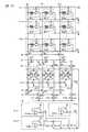
図10は、本発明の一実施の形態による半導体装置において、そのメモリアレー構成を含めた詳細な構成の一例を示す回路図である。図10において、MC11〜MCmnはメモリセルであり、これが2次元的に配列されてメモリアレーMAを構成している。各々のメモリセルMC11〜MCmnは、相変化素子P11〜PmnとMOSトランジスタM11〜Mmnとで構成されており、ワード線WL1〜WLn、ビット線BL1〜BLm、およびソース線SL1〜SLnで、メモリセルMC11〜MCmnのいずれかを選択することができるようになっている。 FIG. 10 is a circuit diagram showing an example of a detailed configuration including the memory array configuration in the semiconductor device according to one embodiment of the present invention. In FIG. 10, MC11 to MCmn are memory cells, which are two-dimensionally arranged to constitute a memory array MA. Each of the memory cells MC11 to MCmn is composed of phase change elements P11 to Pmn and MOS transistors M11 to Mmn, and each of the memory cells includes word lines WL1 to WLn, bit lines BL1 to BLm, and source lines SL1 to SLn. Any one of MC11 to MCmn can be selected.
AM1〜AMmは、ビット線BL1〜BLmの信号を増幅する所謂クロスカップル型のアンプであり、図1等でのセンスアンプSAに該当するものである。SAP,SANはセンスアンプ起動信号である。また、MP1〜MPmは、プリチャージ信号PCによって制御され、ビット線BL1〜BLmをプリチャージ電圧VPCにプリチャージするMOSトランジスタであり、MS1〜MSmは、シェアード信号SHによって制御され、ビット線BL1〜BLmとアンプAM1〜AMmとを接続するMOSトランジスタであり、MR1〜MRmは、センスアンプレファレンス信号SRによって制御され、アンプAM1〜AMmにレファレンス電圧VRFを与えるMOSトランジスタである。 AM1 to AMm are so-called cross-coupled amplifiers that amplify the signals of the bit lines BL1 to BLm, and correspond to the sense amplifier SA in FIG. SAP and SAN are sense amplifier activation signals. MP1 to MPm are MOS transistors that are controlled by the precharge signal PC and precharge the bit lines BL1 to BLm to the precharge voltage VPC. MS1 to MSm are controlled by the shared signal SH and The MOS transistors that connect BLm and the amplifiers AM1 to AMm are MR transistors that are controlled by the sense amplifier reference signal SR and apply the reference voltage VRF to the amplifiers AM1 to AMm.
MOSトランジスタMS1〜MSmによって隔てられ、ビット線BL1〜BLmに対応するアンプ側のビット線が、B11〜Bm1である。また、MD1〜MDmは、ディスチャージ信号DCによって制御され、アンプAM1〜AMm内のレファレンスと反対の端子(すなわち、アンプ側のビット線B11〜Bm1)を接地電圧VssへディスチャージするMOSトランジスタである。また、このアンプAM1〜AMmのレファレンスと接続されている側の端子は、Y選択信号YSで制御されるMOSトランジスタMY11〜MYm1と、これに直列に接続され、Yアドレス信号AY1k〜AYmkが入力されたMOSトランジスタMY12〜MYm2を介してIO線IOに接続されている。 The bit lines on the amplifier side that are separated by the MOS transistors MS1 to MSm and correspond to the bit lines BL1 to BLm are B11 to Bm1. MD1 to MDm are MOS transistors that are controlled by a discharge signal DC and discharge terminals opposite to the reference in the amplifiers AM1 to AMm (that is, the bit lines B11 to Bm1 on the amplifier side) to the ground voltage Vss. The terminals connected to the reference of the amplifiers AM1 to AMm are connected in series to the MOS transistors MY11 to MYm1 controlled by the Y selection signal YS, and the Y address signals AY1k to AYmk are input thereto. The MOS transistors MY12 to MYm2 are connected to the IO line IO.
更に、これは本発明の特徴を表す構成の一例であるが、リセット用電圧VR1、読出し用電圧VY1、セット用電圧VS1を発生する電源VG_rst、VG_rd、VG_setがあり、各々の電源回路は、必要な電圧に対応したVR1用基準電源Vrefreset、VY1用基準電源Vrefread、VS1用基準電源Vrefsetと、各々のアンプと各々の出力トランジスタとからなる。 Furthermore, this is an example of a configuration that represents the feature of the present invention, but there are power supplies VG_rst, VG_rd, and VG_set that generate a reset voltage VR1, a read voltage VY1, and a set voltage VS1, and each power supply circuit is necessary. VR1 reference power supply Vrefreset corresponding to various voltages, VY1 reference power supply Vrefread, VS1 reference power supply Vrefset, each amplifier, and each output transistor.
これらの電圧VR1,VY1,VS1は、スイッチ信号DS1,DS2,DS31,DS32によって制御させるMOSトランジスタによって、選択的にアンプAM1〜AMmの電源に印加することができるようになっている。ここでは、電圧VR1にスイッチ信号DS1を対応させ、電圧VY1にスイッチ信号DS2を対応させ、電圧VS1にスイッチ信号DS31またはDS32を対応させている。このような構成によって、所望の電源電圧をアンプAM1〜AMmを介してビット線BL1〜BLm,BL11〜BLm1に印加できることとなり、これまでの説明で述べてきた機能が実現できるのである。 These voltages VR1, VY1, and VS1 can be selectively applied to the power supplies of the amplifiers AM1 to AMm by MOS transistors controlled by switch signals DS1, DS2, DS31, and DS32. Here, the switch signal DS1 is associated with the voltage VR1, the switch signal DS2 is associated with the voltage VY1, and the switch signal DS31 or DS32 is associated with the voltage VS1. With such a configuration, a desired power supply voltage can be applied to the bit lines BL1 to BLm and BL11 to BLm1 via the amplifiers AM1 to AMm, and the functions described in the above description can be realized.
図11は、図10の構成を用いた動作の一例を示す波形図である。図11では、読出し動作READ、リセット動作RESET、セット動作SET、テスト動作TESTが示されている。まず、READ動作では、スイッチ信号DS1が切り替わり、VY1の電圧が選択される。ここでシェアード信号SHとディスチャージ信号DCが高レベルから低レベルとなり、ビット線BL1〜BLm,BL11〜BLm1がVssにディスチャージされた状態でフローティングとなる。 FIG. 11 is a waveform diagram showing an example of an operation using the configuration of FIG. In FIG. 11, a read operation READ, a reset operation RESET, a set operation SET, and a test operation TEST are shown. First, in the READ operation, the switch signal DS1 is switched and the voltage of VY1 is selected. Here, the shared signal SH and the discharge signal DC are changed from the high level to the low level, and the bit lines BL1 to BLm and BL11 to BLm1 are floated in a state where they are discharged to Vss.
この状態で、再びシェアード信号SHが切り替わり、またプリチャージ信号PCとセンスアンプリファレンス信号SRとが切り替わりビット線BL1〜BLm,BL11〜BLm1はVPCにプリチャージされ、この電圧VPCはアンプAM1〜AMmの一方の入力となり、他方の入力はVRFにプリチャージされる。この後、選択されたワード線WL1が切り替わり、ビット線BL1〜BLmに信号が現われる。すなわち、相変化素子では抵抗が高い状態と低い状態とを取りうるので、これに応じた信号が読み出される。この信号は、センスアンプ起動信号SAN,SAPが切り替わることによって、アンプAM1〜AMmが活性化され、増幅される。この増幅信号を取り出すために、Y選択信号YSと選択されたYアドレス信号AY1kが切り替わる。これによってIO線IOに読み出された信号が出力される。 In this state, the shared signal SH is switched again, the precharge signal PC and the sense amplifier reference signal SR are switched, and the bit lines BL1 to BLm and BL11 to BLm1 are precharged to VPC, and this voltage VPC is applied to the amplifiers AM1 to AMm. One input is precharged to VRF. Thereafter, the selected word line WL1 is switched, and a signal appears on the bit lines BL1 to BLm. That is, since the phase change element can have a high resistance state and a low resistance state, a signal corresponding to this can be read out. This signal is amplified by activating the amplifiers AM1 to AMm when the sense amplifier activation signals SAN and SAP are switched. In order to extract this amplified signal, the Y selection signal YS and the selected Y address signal AY1k are switched. As a result, the read signal is output to the IO line IO.
リセット動作RESETでは、今度はスイッチ信号DS2が切り替わり、VR1の電圧が選択される。最初のディスチャージが解除された後、シェアード信号SH、センスアンプ起動信号SAN,SAPが切り替わり、ビット線(例えばBL1)にはVR1の電圧が印加される。ここで、ワード線WL1が切り替わり、メモリセルトランジスタがオンして、相変化素子に熱が加えられる。これによって、相変化素子(例えばP11)は溶けた状態となる。 In the reset operation RESET, the switch signal DS2 is switched this time, and the voltage of VR1 is selected. After the first discharge is released, the shared signal SH and the sense amplifier activation signals SAN and SAP are switched, and the voltage VR1 is applied to the bit line (for example, BL1). Here, the word line WL1 is switched, the memory cell transistor is turned on, and heat is applied to the phase change element. Thereby, a phase change element (for example, P11) will be in the melted state.
この後、ワード線WL1を立下り時間t1で切り替える。これによって、相変化素子(例えばP11)は熱を与えられなくなり、急速に冷やされ、アモルファス状態となるのである。このアモルファス状態は、電気的には抵抗が高い状態であり、読出し動作READでは、メモリセルトランジスタをオンさせても電流が流れにくく、ビット線の電圧変化が小さい状態である。 Thereafter, the word line WL1 is switched at the fall time t1. As a result, the phase change element (for example, P11) is not given heat, is rapidly cooled, and becomes in an amorphous state. This amorphous state is a state where the resistance is electrically high. In the read operation READ, even if the memory cell transistor is turned on, it is difficult for current to flow, and the voltage change of the bit line is small.
セット動作SETでは、今度はスイッチ信号DS31が切り替わり、VS1の電圧が選択される。この電圧は、一般にVR1よりも低く、VY1よりも高い。これに応じて相変化素子に与えられる熱の大小関係も同様となる。最初のディスチャージが解除された後、シェアード信号SH、センスアンプ起動信号SAN,SAPが切り替わり、ビット(例えばBL1)にはVS1の電圧が印加される。 In the set operation SET, the switch signal DS31 is switched this time, and the voltage of VS1 is selected. This voltage is generally lower than VR1 and higher than VY1. Accordingly, the magnitude relationship of heat given to the phase change element is the same. After the first discharge is released, the shared signal SH and the sense amplifier activation signals SAN and SAP are switched, and the voltage VS1 is applied to the bit (for example, BL1).
ここで、ワード線WL1が切り替わり、メモリセルトランジスタがオンして、相変化素子(例えばP11)に熱が加えられる。この状態をt3の間保持すると、相変化素子(例えばP11)は結晶状態へと変化する。この結晶状態は、電気的には抵抗が低い状態であり、読出し動作READでは、メモリセルトランジスタをオンさせると電流が流れやすく、ビット線の電圧変化が大きい状態である。 Here, the word line WL1 is switched, the memory cell transistor is turned on, and heat is applied to the phase change element (eg, P11). When this state is maintained for t3, the phase change element (for example, P11) changes to a crystalline state. This crystal state is a state where the resistance is electrically low. In the read operation READ, when the memory cell transistor is turned on, a current flows easily and the voltage change of the bit line is large.
テスト動作TESTでは、今度はスイッチ信号DS32が切り替わり、セット動作と同じくVS1の電圧が選択される。このテスト動作では、この電圧下で読出しのタイミングが印加されるのである。このため、相変化素子に印加される時間そのものはt2となる。この時間t2は、正常な相変化素子であれば、結晶化を起こすには充分ではなく、メモリ素子にストレスのみを与える。そして、これによる相変化素子の状態の変化を検知することによって不良か否かを判断できる。相変化素子の状態の変化とは、具体的には、リセット状態の相変化素子に対してこのテスト動作を行い、どの程度セット状態に移ってしまったかを読出し動作で確認することで行なう。 In the test operation TEST, the switch signal DS32 is switched this time, and the voltage VS1 is selected as in the set operation. In this test operation, the read timing is applied under this voltage. For this reason, the time itself applied to the phase change element is t2. This time t2 is not sufficient to cause crystallization if it is a normal phase change element, and only stress is applied to the memory element. And it can be judged whether it is defective by detecting the change of the state of the phase change element by this. Specifically, the change in the state of the phase change element is performed by performing this test operation on the phase change element in the reset state and confirming to what extent the state has been changed to the set state by a read operation.
なお、図10の構成は、例えば図8で示したような構成に基づいて組み立てることもできる。すなわち、テスト用にVT1という電圧とその発生回路を設け、図10に示したDS32(図8ではDS4に相当)で選択できる構成とすれば良い。 Note that the configuration of FIG. 10 can be assembled based on the configuration shown in FIG. 8, for example. In other words, a voltage VT1 and its generation circuit may be provided for testing, and the configuration can be selected with DS32 shown in FIG. 10 (corresponding to DS4 in FIG. 8).
図12は、図10等におけるメモリセルの構成例を示す回路図であり、(a)、(b)はMOSトランジスタと相変化素子とで構成した例、(c−1)、(c−2)、(d−1)、(d−2)は、バイポーラトランジスタと相変化素子とで構成した例を示すものである。図12(a),(b)においては、ビット線BLmとソース線SLnの電圧駆動方法によって、このどちらを選ぶかを決定する。なお、これらのMOSトランジスタは、この図ではnMOSトランジスタとしたが、pMOSトランジスタとすることで、電圧の選択方法によっては制御が簡単になる場合もある。 FIG. 12 is a circuit diagram showing a configuration example of the memory cell in FIG. 10 and the like. (A) and (b) are examples configured with MOS transistors and phase change elements, (c-1), (c-2). ), (D-1), and (d-2) show examples configured with bipolar transistors and phase change elements. In FIGS. 12A and 12B, which one to select is determined depending on the voltage driving method of the bit line BLm and the source line SLn. These MOS transistors are nMOS transistors in this figure, but by using pMOS transistors, control may be simplified depending on the voltage selection method.
図12(c−1),(c−2),(d−1),(d−2)は、共にバイポーラトランジスタのエミッタ端子と相変化素子とを接続する場合を示している。これによって、メモリセル面積を小さく構成することができる。ビット線BLmとソース線SLnの接続の方法は、これらの電圧駆動方法によって、(c−1),(c−2),(d−1),(d−2)のいずれを選ぶかを決定する。 12 (c-1), (c-2), (d-1), and (d-2) all show a case where the emitter terminal of the bipolar transistor and the phase change element are connected. Thereby, the memory cell area can be reduced. The method of connecting the bit line BLm and the source line SLn determines which of (c-1), (c-2), (d-1), and (d-2) is selected according to these voltage driving methods. To do.
図13は、本発明の一実施の形態による半導体装置において、その構成の一例を示す断面図である。一般に相変化メモリLSIでは、IO回路などでは比較的高い電圧が外部から印加され、例えばデコーダ回路や他の論理回路ではそれよりも低い電圧が印加される。この実施の形態では、これに応じて、比較的高い電圧が印加される部分には、酸化絶縁膜の厚いMOSトランジスタを使用する。これが、MP_IOとMN_IOであり、これらの酸化絶縁膜部分がそれぞれSIO4とSIO3である。 FIG. 13 is a cross-sectional view showing an example of the configuration of a semiconductor device according to an embodiment of the present invention. In general, in a phase change memory LSI, a relatively high voltage is applied from the outside in an IO circuit or the like, and a lower voltage is applied in a decoder circuit or other logic circuit, for example. In this embodiment, a MOS transistor having a thick oxide insulating film is used for a portion to which a relatively high voltage is applied. These are MP_IO and MN_IO, and these oxide insulating film portions are SIO4 and SIO3, respectively.
また、低い電圧が印加される部分には酸化絶縁膜の薄いMOSトランジスタを使用する。これが、MP_COREとMN_COREであり、これらの酸化絶縁膜部分がそれぞれSIO2とSIO1である。メモリセルのMOSトランジスタはMN_MEMであり、その酸化絶縁膜部分はSIO0である。このSIO0は、SIO1と同じ膜厚とするとより小さなセル面積を容易に実現できるようになり、またSIO3とすると扱える電圧範囲を広くすることができる。 A MOS transistor having a thin oxide insulating film is used for a portion to which a low voltage is applied. These are MP_CORE and MN_CORE, and these oxide insulating film portions are SIO2 and SIO1, respectively. The MOS transistor of the memory cell is MN_MEM, and the oxide insulating film portion is SIO0. If the SIO0 has the same film thickness as the SIO1, a smaller cell area can be easily realized, and if it is SIO3, the voltage range that can be handled can be widened.
相変化素子(PCR)は、この図では、MN_MEMのソース/ドレイン領域(n+)の一方より、コンタククト層(CNT)とメタル第1層(ML1)ともうひとつコンタクト層(CNT)に片面を接し、メタル第2層(ML2)に多面を接して、この2層に挟まれた形となっている。ソース/ドレイン領域(n+)の他方は、メタル第3層(ML3)まで接続されている。各トランジスタは、この図では、素子分離用絶縁膜(FI)で分離されており、各々のゲートはポリシリコン膜(Poly−Si)で形成されている。また、この図では示していないが、シリサイド又はサリサイド(セルフアラインでのシリサイド)を用いて、ソース/ドレイン領域又は、ゲートとソース/ドレイン領域の抵抗を下げる場合もある。 In this figure, the phase change element (PCR) is in contact with one side of the contact layer (CNT), the metal first layer (ML1), and the other contact layer (CNT) from one of the source / drain regions (n +) of the MN_MEM. The metal second layer (ML2) is in contact with many faces and is sandwiched between the two layers. The other of the source / drain regions (n +) is connected to the third metal layer (ML3). In this figure, each transistor is separated by an element isolation insulating film (FI), and each gate is formed by a polysilicon film (Poly-Si). Although not shown in this figure, silicide or salicide (silicide in self-alignment) may be used to lower the resistance of the source / drain region or the gate and source / drain region.
図14は、本発明の一実施の形態による半導体装置において、図13とは異なる構成の一例を示す断面図である。図13と異なる点は、メモリセルにおいてバイポーラトランジスタを用いて構成した点である。このバイポーラトランジスタは、エミッタ層(n+)とベース層(p)とコレクタ層(NWELL)とを用いた、npn型バイポーラトランジスタとなっており、そのエミッタ層(n+)よりコンタクト層(CNT)とメタル第1層(ML1)ともうひとつコンタクト層(CNT)を介して相変化素子(PCR)と接続している。ベース層(p)からはコンタククト層(CNT)とメタル第1層(ML1)とで電極を引き出した図を示している。コレクタ層(NWELL)からは、この図面には示していないが、この図面と垂直な方向にコレクタ領域が延び、コンタククト層を介して電極が引き出される。複数のメモリセルでこのコレクタ層を共有する場合もある。 FIG. 14 is a cross-sectional view showing an example of a configuration different from FIG. 13 in the semiconductor device according to the embodiment of the present invention. The difference from FIG. 13 is that the memory cell is configured using bipolar transistors. This bipolar transistor is an npn-type bipolar transistor using an emitter layer (n +), a base layer (p), and a collector layer (NWELL). A contact layer (CNT) and a metal are formed from the emitter layer (n +). The phase change element (PCR) is connected via the first layer (ML1) and another contact layer (CNT). From the base layer (p), the figure which extracted the electrode by the contact layer (CNT) and the metal 1st layer (ML1) is shown. Although not shown in the drawing, the collector region extends in a direction perpendicular to the drawing from the collector layer (NWELL), and an electrode is drawn out through the contact layer. A plurality of memory cells may share this collector layer.
以上、本発明者によってなされた発明を実施の形態に基づき具体的に説明したが、本発明は前記実施の形態に限定されるものではなく、その要旨を逸脱しない範囲で種々変更可能であることはいうまでもない。 As mentioned above, the invention made by the present inventor has been specifically described based on the embodiment. However, the present invention is not limited to the embodiment, and various modifications can be made without departing from the scope of the invention. Needless to say.
本発明の半導体装置は、特に相変化材料を用いた例えば、高密度集積メモリ回路、およびメモリ回路と論理回路が同一半導体基板に設けられたロジック混載型メモリ、およびアナログ回路を有する半導体装置に適用して有益な技術である。 The semiconductor device of the present invention is applied to, for example, a high-density integrated memory circuit using a phase change material, a logic embedded memory in which a memory circuit and a logic circuit are provided on the same semiconductor substrate, and a semiconductor device having an analog circuit. It is a useful technique.
VG_rd 読出しビット線電圧電源
VG_rst リセット用ビット線電圧電源
VG_set セット用ビット線電圧電源
TG_rd_test 読出し/テスト時タイミング発生回路
TG_set セット時タイミング発生回路
TG_rst リセット時タイミング発生回路
TG_rd 読出し時タイミング発生回路
Test_ctl テスト制御回路
Set_ctl セット制御回路
Rst_ctl リセット制御回路
Read_ctl 読出し制御回路
SD ソースドライバ
SA センスアンプ
WD ワードドライバ
WL,WL1〜WLn ワード線
BL,BL1〜BLm ビット線
SL,SL1〜SLn ソース線
P1,P11〜Pmn,PCR 相変化素子
M1,M11〜Mmn,MS1〜MSm,MP1〜MPm,MR1〜MRm,MD1〜MDm,MY11〜MYm1,MY12〜MYm2 MOSトランジスタ
Q1,Qmn バイポーラトランジスタ
MC,MC11〜MCmn メモリセル
MA メモリアレー
VY1 読出し用電圧
VR1 リセット用電圧
VS1 セット用電圧
SW1,SW2,SW3 スイッチ
DS1,DS2,DS3,DS31,DS32 スイッチ信号
SH シェアード信号
PC プリチャージ信号
SR センスアンプレファレンス信号
SAN,SAP センスアンプ起動信号
AM1〜AMm アンプ
DC ディスチャージ信号
YS Y選択信号
AY1k〜AYmk Yアドレス信号
IO IO線
MP_IO,MN_IO IO用トランジスタ
MP_CORE,MN_CORE コア用トランジスタ
MN_MEM メモリセル用トランジスタ
ML1,ML2,ML3 メタル層
SIO1〜4 酸化絶縁膜
CNT コンタククト層
n+,p+ 拡散層
NWELL,PWELL ウェル
FI 素子分離用絶縁膜
Poly−Si ポリシリコン膜VG_rd Read bit line voltage power supply VG_rst Reset bit line voltage power supply VG_set Set bit line voltage power supply TG_rd_test Read / test timing generation circuit TG_set Set timing generation circuit TG_rst Reset timing generation circuit TG_rd Read timing generation circuit Test control circuit Set_ctl Set control circuit Rst_ctl Reset control circuit Read_ctl Read control circuit SD source driver SA sense amplifier WD Word driver WL, WL1 to WLn Word line BL, BL1 to BLm Bit line SL, SL1 to SLn Source lines P1, P11 to Pmn, PCR phase Change elements M1, M11 to Mmn, MS1 to MSm, MP1 to MPm, MR1 to MRm, MD1 MDm, MY11 to MYm1, MY12 to MYm2 MOS transistor Q1, Qmn Bipolar transistor MC, MC11 to MCmn Memory cell MA Memory array VY1 Read voltage VR1 Reset voltage VS1 Set voltage SW1, SW2, SW3 Switch DS1, DS2, DS3 DS31, DS32 switch signal SH shared signal PC precharge signal SR sense amplifier reference signal SAN, SAP sense amplifier activation signal AM1-AMm amplifier DC discharge signal YSY selection signal AY1k-AYmk Y address signal IO IO line MP_IO, MN_IO IO transistor MP_CORE, MN_CORE Core transistor MN_MEM Memory cell transistor ML1, ML2, ML3 Tal layer SIO1~4 oxide insulating film CNT Kontakukuto layer n +, p + diffusion layer NWELL, PWELL well FI isolation insulating film Poly-Si polysilicon film
Claims (9)
Translated fromJapanese前記複数のメモリセルのそれぞれは、結晶化状態と非晶質状態との抵抗値の違いを利用してデータを記憶するメモリ素子を備え、
前記半導体装置のテスト動作の際に、前記メモリ素子に対し、結晶化状態を作り出す時に前記メモリ素子に印加する電圧と同じ第1電圧を、結晶化状態を作り出す時に前記メモリ素子に電圧を印加する時間よりも短い第1時間だけ印加することを特徴とする半導体装置。A semiconductor device including a plurality of memory cells,
Each of the plurality of memory cells includes a memory element that stores data using a difference in resistance value between a crystallized state and an amorphous state,
During a test operation of the semiconductor device, a first voltage that is the same as a voltage applied to the memory element when creating a crystallized state is applied to the memory element, and a voltage is applied to the memory element when creating a crystallized state. A semiconductor device, which is applied only for a first time shorter than the time.
前記第1電圧は、前記メモリ素子を結晶化状態にする際に用いる電圧発生回路を共有することで生成されることを特徴とする半導体装置。The semiconductor device according to claim 1,
The semiconductor device, wherein the first voltage is generated by sharing a voltage generation circuit used when the memory element is brought into a crystallized state.
前記第1時間は、読出し動作を行なう時に前記メモリ素子に電圧を印加する時間と同じ時間であり、前記メモリ素子に対して読出し動作を行う際に用いるタイミング発生回路を共有することで生成されることを特徴とする半導体装置。The semiconductor device according to claim 2,
The first time is the same as the time during which a voltage is applied to the memory element when performing a read operation, and is generated by sharing a timing generation circuit used when performing a read operation on the memory element. A semiconductor device.
前記複数のメモリセルのそれぞれは、結晶化状態と非晶質状態との抵抗値の違いを利用してデータを記憶するメモリ素子を備え、
前記半導体装置のテスト動作の際に、前記メモリ素子に対し、読出し動作を行なう時に前記メモリ素子に印加する電圧よりも高く、前記結晶化状態を作り出す時に前記メモリ素子に印加する電圧よりも低い第2電圧を、読出し動作を行なう時に前記メモリ素子に電圧を印加する時間と同じ第2時間だけ印加することを特徴とする半導体装置。A semiconductor device including a plurality of memory cells,
Each of the plurality of memory cells includes a memory element that stores data using a difference in resistance value between a crystallized state and an amorphous state,
During a test operation of the semiconductor device, a voltage higher than a voltage applied to the memory element when performing a read operation on the memory element and lower than a voltage applied to the memory element when creating the crystallized state. 2. A semiconductor device, wherein two voltages are applied for a second time that is equal to a time during which a voltage is applied to the memory element when a read operation is performed.
前記第2時間は、前記メモリ素子に対して読出し動作を行う際に用いるタイミング発生回路を共有することで生成されることを特徴とする半導体装置。The semiconductor device according to claim 4.
The semiconductor device according to claim 1, wherein the second time is generated by sharing a timing generation circuit used when a read operation is performed on the memory element.
前記第2電圧は、外部端子より入力されることを特徴とする半導体装置。The semiconductor device according to claim 4.
The semiconductor device, wherein the second voltage is input from an external terminal.
前記複数のメモリセルのそれぞれは、結晶化状態と非晶質状態との抵抗値の違いを利用してデータを記憶するメモリ素子を備え、
前記半導体装置のテスト動作の際に、前記メモリ素子に対し、読出し動作を行なう時に前記メモリ素子に印加する電圧と同じ第3電圧を、前記結晶化状態を作り出す時に前記メモリ素子に電圧を印加する時間と同じ第3時間だけ印加することを特徴とする半導体装置。A semiconductor device including a plurality of memory cells,
Each of the plurality of memory cells includes a memory element that stores data using a difference in resistance value between a crystallized state and an amorphous state,
During a test operation of the semiconductor device, a third voltage that is the same as a voltage applied to the memory element when a read operation is performed is applied to the memory element, and a voltage is applied to the memory element when the crystallization state is created. A semiconductor device which is applied only for a third time which is the same as the time.
前記第3電圧は、前記メモリ素子に対して読出し動作を行う際に用いる電圧発生回路を共有することで生成され、
前記第3時間は、前記メモリ素子を結晶化状態にする際に用いるタイミング発生回路を共有することで生成されることを特徴とする半導体装置。The semiconductor device according to claim 7.
The third voltage is generated by sharing a voltage generation circuit used when performing a read operation on the memory element,
The semiconductor device is characterized in that the third time is generated by sharing a timing generation circuit used when the memory element is brought into a crystallized state.
前記メモリ素子は、カルコゲナイド材料を含むことを特徴とする半導体装置。The semiconductor device according to claim 1, wherein:
The memory device includes a chalcogenide material.
Priority Applications (2)
| Application Number | Priority Date | Filing Date | Title |
|---|---|---|---|
| JP2005056010AJP2006244561A (en) | 2005-03-01 | 2005-03-01 | Semiconductor apparatus |
| US11/337,648US20060198183A1 (en) | 2005-03-01 | 2006-01-24 | Semiconductor device |
Applications Claiming Priority (1)
| Application Number | Priority Date | Filing Date | Title |
|---|---|---|---|
| JP2005056010AJP2006244561A (en) | 2005-03-01 | 2005-03-01 | Semiconductor apparatus |
Publications (1)
| Publication Number | Publication Date |
|---|---|
| JP2006244561Atrue JP2006244561A (en) | 2006-09-14 |
Family
ID=36943968
Family Applications (1)
| Application Number | Title | Priority Date | Filing Date |
|---|---|---|---|
| JP2005056010APendingJP2006244561A (en) | 2005-03-01 | 2005-03-01 | Semiconductor apparatus |
Country Status (2)
| Country | Link |
|---|---|
| US (1) | US20060198183A1 (en) |
| JP (1) | JP2006244561A (en) |
Cited By (5)
| Publication number | Priority date | Publication date | Assignee | Title |
|---|---|---|---|---|
| WO2008035392A1 (en)* | 2006-09-19 | 2008-03-27 | Renesas Technology Corp. | Semiconductor integrated circuit device |
| WO2009008080A1 (en)* | 2007-07-12 | 2009-01-15 | Renesas Technology Corp. | Semiconductor device |
| JPWO2008041278A1 (en)* | 2006-09-29 | 2010-01-28 | 株式会社ルネサステクノロジ | Semiconductor device |
| US7848165B2 (en) | 2008-01-09 | 2010-12-07 | Samsung Electronics Co., Ltd. | Methods of operating phase-change random access memory devices |
| JP2011028799A (en)* | 2009-07-23 | 2011-02-10 | Toshiba Corp | Test device and test method for resistive random access memory, and resistive random access memory device |
Families Citing this family (77)
| Publication number | Priority date | Publication date | Assignee | Title |
|---|---|---|---|---|
| US7635855B2 (en) | 2005-11-15 | 2009-12-22 | Macronix International Co., Ltd. | I-shaped phase change memory cell |
| US7786460B2 (en) | 2005-11-15 | 2010-08-31 | Macronix International Co., Ltd. | Phase change memory device and manufacturing method |
| US7449710B2 (en) | 2005-11-21 | 2008-11-11 | Macronix International Co., Ltd. | Vacuum jacket for phase change memory element |
| US7599217B2 (en) | 2005-11-22 | 2009-10-06 | Macronix International Co., Ltd. | Memory cell device and manufacturing method |
| US7688619B2 (en)* | 2005-11-28 | 2010-03-30 | Macronix International Co., Ltd. | Phase change memory cell and manufacturing method |
| US7459717B2 (en) | 2005-11-28 | 2008-12-02 | Macronix International Co., Ltd. | Phase change memory cell and manufacturing method |
| US7531825B2 (en) | 2005-12-27 | 2009-05-12 | Macronix International Co., Ltd. | Method for forming self-aligned thermal isolation cell for a variable resistance memory array |
| US8062833B2 (en) | 2005-12-30 | 2011-11-22 | Macronix International Co., Ltd. | Chalcogenide layer etching method |
| US7741636B2 (en) | 2006-01-09 | 2010-06-22 | Macronix International Co., Ltd. | Programmable resistive RAM and manufacturing method |
| US7560337B2 (en) | 2006-01-09 | 2009-07-14 | Macronix International Co., Ltd. | Programmable resistive RAM and manufacturing method |
| US7785920B2 (en) | 2006-07-12 | 2010-08-31 | Macronix International Co., Ltd. | Method for making a pillar-type phase change memory element |
| US7504653B2 (en) | 2006-10-04 | 2009-03-17 | Macronix International Co., Ltd. | Memory cell device with circumferentially-extending memory element |
| US7863655B2 (en) | 2006-10-24 | 2011-01-04 | Macronix International Co., Ltd. | Phase change memory cells with dual access devices |
| US7476587B2 (en) | 2006-12-06 | 2009-01-13 | Macronix International Co., Ltd. | Method for making a self-converged memory material element for memory cell |
| US7903447B2 (en) | 2006-12-13 | 2011-03-08 | Macronix International Co., Ltd. | Method, apparatus and computer program product for read before programming process on programmable resistive memory cell |
| US7839672B1 (en) | 2006-12-18 | 2010-11-23 | Marvell International Ltd. | Phase change memory array circuits and methods of manufacture |
| US7718989B2 (en) | 2006-12-28 | 2010-05-18 | Macronix International Co., Ltd. | Resistor random access memory cell device |
| US7515461B2 (en)* | 2007-01-05 | 2009-04-07 | Macronix International Co., Ltd. | Current compliant sensing architecture for multilevel phase change memory |
| US7956344B2 (en) | 2007-02-27 | 2011-06-07 | Macronix International Co., Ltd. | Memory cell with memory element contacting ring-shaped upper end of bottom electrode |
| US7786461B2 (en) | 2007-04-03 | 2010-08-31 | Macronix International Co., Ltd. | Memory structure with reduced-size memory element between memory material portions |
| US7569844B2 (en)* | 2007-04-17 | 2009-08-04 | Macronix International Co., Ltd. | Memory cell sidewall contacting side electrode |
| US20080263415A1 (en)* | 2007-04-17 | 2008-10-23 | Bernhard Ruf | Integrated Circuit, Memory Module, Method of Operating an Integrated Circuit, Method of Fabricating an Integrated Circuit, Computer Program Product, and Computing System |
| US7864565B2 (en)* | 2007-07-31 | 2011-01-04 | Infineon Technologies Ag | Data retention monitor |
| US7729161B2 (en) | 2007-08-02 | 2010-06-01 | Macronix International Co., Ltd. | Phase change memory with dual word lines and source lines and method of operating same |
| US7919766B2 (en) | 2007-10-22 | 2011-04-05 | Macronix International Co., Ltd. | Method for making self aligning pillar memory cell device |
| US7715258B2 (en)* | 2007-12-21 | 2010-05-11 | Qimonda Ag | Retention test system and method for resistively switching memory devices |
| DE102007062092A1 (en)* | 2007-12-21 | 2009-07-02 | Qimonda Ag | Data holding test executing system for resistive switching memory device i.e. conductive bridging RAM memory device, has applies bias voltage to conductive bridging RAM memory cell of memory device, before or during data holding test |
| US8084842B2 (en) | 2008-03-25 | 2011-12-27 | Macronix International Co., Ltd. | Thermally stabilized electrode structure |
| US8030634B2 (en)* | 2008-03-31 | 2011-10-04 | Macronix International Co., Ltd. | Memory array with diode driver and method for fabricating the same |
| US7825398B2 (en) | 2008-04-07 | 2010-11-02 | Macronix International Co., Ltd. | Memory cell having improved mechanical stability |
| US7791057B2 (en) | 2008-04-22 | 2010-09-07 | Macronix International Co., Ltd. | Memory cell having a buried phase change region and method for fabricating the same |
| US8077505B2 (en) | 2008-05-07 | 2011-12-13 | Macronix International Co., Ltd. | Bipolar switching of phase change device |
| US7701750B2 (en) | 2008-05-08 | 2010-04-20 | Macronix International Co., Ltd. | Phase change device having two or more substantial amorphous regions in high resistance state |
| US8415651B2 (en) | 2008-06-12 | 2013-04-09 | Macronix International Co., Ltd. | Phase change memory cell having top and bottom sidewall contacts |
| US8134857B2 (en)* | 2008-06-27 | 2012-03-13 | Macronix International Co., Ltd. | Methods for high speed reading operation of phase change memory and device employing same |
| US7932506B2 (en) | 2008-07-22 | 2011-04-26 | Macronix International Co., Ltd. | Fully self-aligned pore-type memory cell having diode access device |
| US7903457B2 (en) | 2008-08-19 | 2011-03-08 | Macronix International Co., Ltd. | Multiple phase change materials in an integrated circuit for system on a chip application |
| US7719913B2 (en) | 2008-09-12 | 2010-05-18 | Macronix International Co., Ltd. | Sensing circuit for PCRAM applications |
| US8324605B2 (en) | 2008-10-02 | 2012-12-04 | Macronix International Co., Ltd. | Dielectric mesh isolated phase change structure for phase change memory |
| US7897954B2 (en) | 2008-10-10 | 2011-03-01 | Macronix International Co., Ltd. | Dielectric-sandwiched pillar memory device |
| US8036014B2 (en) | 2008-11-06 | 2011-10-11 | Macronix International Co., Ltd. | Phase change memory program method without over-reset |
| US7885101B2 (en)* | 2008-12-29 | 2011-02-08 | Numonyx B.V. | Method for low-stress multilevel reading of phase change memory cells and multilevel phase change memory |
| US7869270B2 (en) | 2008-12-29 | 2011-01-11 | Macronix International Co., Ltd. | Set algorithm for phase change memory cell |
| US8089137B2 (en) | 2009-01-07 | 2012-01-03 | Macronix International Co., Ltd. | Integrated circuit memory with single crystal silicon on silicide driver and manufacturing method |
| US8107283B2 (en) | 2009-01-12 | 2012-01-31 | Macronix International Co., Ltd. | Method for setting PCRAM devices |
| US8030635B2 (en) | 2009-01-13 | 2011-10-04 | Macronix International Co., Ltd. | Polysilicon plug bipolar transistor for phase change memory |
| US8064247B2 (en) | 2009-01-14 | 2011-11-22 | Macronix International Co., Ltd. | Rewritable memory device based on segregation/re-absorption |
| US8933536B2 (en) | 2009-01-22 | 2015-01-13 | Macronix International Co., Ltd. | Polysilicon pillar bipolar transistor with self-aligned memory element |
| US8084760B2 (en)* | 2009-04-20 | 2011-12-27 | Macronix International Co., Ltd. | Ring-shaped electrode and manufacturing method for same |
| US8173987B2 (en) | 2009-04-27 | 2012-05-08 | Macronix International Co., Ltd. | Integrated circuit 3D phase change memory array and manufacturing method |
| US8097871B2 (en) | 2009-04-30 | 2012-01-17 | Macronix International Co., Ltd. | Low operational current phase change memory structures |
| US7933139B2 (en) | 2009-05-15 | 2011-04-26 | Macronix International Co., Ltd. | One-transistor, one-resistor, one-capacitor phase change memory |
| US7968876B2 (en) | 2009-05-22 | 2011-06-28 | Macronix International Co., Ltd. | Phase change memory cell having vertical channel access transistor |
| US8350316B2 (en)* | 2009-05-22 | 2013-01-08 | Macronix International Co., Ltd. | Phase change memory cells having vertical channel access transistor and memory plane |
| US8809829B2 (en) | 2009-06-15 | 2014-08-19 | Macronix International Co., Ltd. | Phase change memory having stabilized microstructure and manufacturing method |
| US8406033B2 (en) | 2009-06-22 | 2013-03-26 | Macronix International Co., Ltd. | Memory device and method for sensing and fixing margin cells |
| US8363463B2 (en) | 2009-06-25 | 2013-01-29 | Macronix International Co., Ltd. | Phase change memory having one or more non-constant doping profiles |
| US8238149B2 (en) | 2009-06-25 | 2012-08-07 | Macronix International Co., Ltd. | Methods and apparatus for reducing defect bits in phase change memory |
| US8198619B2 (en) | 2009-07-15 | 2012-06-12 | Macronix International Co., Ltd. | Phase change memory cell structure |
| US8110822B2 (en) | 2009-07-15 | 2012-02-07 | Macronix International Co., Ltd. | Thermal protect PCRAM structure and methods for making |
| US7894254B2 (en) | 2009-07-15 | 2011-02-22 | Macronix International Co., Ltd. | Refresh circuitry for phase change memory |
| US8064248B2 (en) | 2009-09-17 | 2011-11-22 | Macronix International Co., Ltd. | 2T2R-1T1R mix mode phase change memory array |
| US8178387B2 (en) | 2009-10-23 | 2012-05-15 | Macronix International Co., Ltd. | Methods for reducing recrystallization time for a phase change material |
| US8729521B2 (en) | 2010-05-12 | 2014-05-20 | Macronix International Co., Ltd. | Self aligned fin-type programmable memory cell |
| US8310864B2 (en) | 2010-06-15 | 2012-11-13 | Macronix International Co., Ltd. | Self-aligned bit line under word line memory array |
| JP2012038387A (en)* | 2010-08-06 | 2012-02-23 | Toshiba Corp | Semiconductor memory device |
| US8194441B2 (en)* | 2010-09-23 | 2012-06-05 | Micron Technology, Inc. | Phase change memory state determination using threshold edge detection |
| US8395935B2 (en) | 2010-10-06 | 2013-03-12 | Macronix International Co., Ltd. | Cross-point self-aligned reduced cell size phase change memory |
| US8497705B2 (en) | 2010-11-09 | 2013-07-30 | Macronix International Co., Ltd. | Phase change device for interconnection of programmable logic device |
| US8467238B2 (en) | 2010-11-15 | 2013-06-18 | Macronix International Co., Ltd. | Dynamic pulse operation for phase change memory |
| US8987700B2 (en) | 2011-12-02 | 2015-03-24 | Macronix International Co., Ltd. | Thermally confined electrode for programmable resistance memory |
| US9336879B2 (en) | 2014-01-24 | 2016-05-10 | Macronix International Co., Ltd. | Multiple phase change materials in an integrated circuit for system on a chip application |
| US9559113B2 (en) | 2014-05-01 | 2017-01-31 | Macronix International Co., Ltd. | SSL/GSL gate oxide in 3D vertical channel NAND |
| US9625325B2 (en)* | 2015-02-18 | 2017-04-18 | Globalfoundries Inc. | System and method for identifying operating temperatures and modifying of integrated circuits |
| US9672906B2 (en) | 2015-06-19 | 2017-06-06 | Macronix International Co., Ltd. | Phase change memory with inter-granular switching |
| CN106024054A (en)* | 2016-05-24 | 2016-10-12 | 中国科学院上海微系统与信息技术研究所 | Phase change memory with retention test function |
| KR102667819B1 (en)* | 2019-07-11 | 2024-05-21 | 삼성전자주식회사 | Memory device comprising switch circuit that operates regardless of power supply voltage |
- 2005
- 2005-03-01JPJP2005056010Apatent/JP2006244561A/enactivePending
- 2006
- 2006-01-24USUS11/337,648patent/US20060198183A1/ennot_activeAbandoned
Cited By (6)
| Publication number | Priority date | Publication date | Assignee | Title |
|---|---|---|---|---|
| WO2008035392A1 (en)* | 2006-09-19 | 2008-03-27 | Renesas Technology Corp. | Semiconductor integrated circuit device |
| JPWO2008035392A1 (en)* | 2006-09-19 | 2010-01-28 | 株式会社ルネサステクノロジ | Semiconductor integrated circuit device |
| JPWO2008041278A1 (en)* | 2006-09-29 | 2010-01-28 | 株式会社ルネサステクノロジ | Semiconductor device |
| WO2009008080A1 (en)* | 2007-07-12 | 2009-01-15 | Renesas Technology Corp. | Semiconductor device |
| US7848165B2 (en) | 2008-01-09 | 2010-12-07 | Samsung Electronics Co., Ltd. | Methods of operating phase-change random access memory devices |
| JP2011028799A (en)* | 2009-07-23 | 2011-02-10 | Toshiba Corp | Test device and test method for resistive random access memory, and resistive random access memory device |
Also Published As
| Publication number | Publication date |
|---|---|
| US20060198183A1 (en) | 2006-09-07 |
Similar Documents
| Publication | Publication Date | Title |
|---|---|---|
| JP2006244561A (en) | Semiconductor apparatus | |
| TWI398867B (en) | Semiconductor device | |
| US8891293B2 (en) | High-endurance phase change memory devices and methods for operating the same | |
| JP4669518B2 (en) | Semiconductor device | |
| KR101926603B1 (en) | Semiconductor memory device and Burn-in test method thereof | |
| JP6005343B2 (en) | Method of writing MRAM-based memory device with reduced power consumption | |
| JP4861444B2 (en) | Forming method of variable resistance element | |
| JP2010257551A (en) | Antifuse memory cell and semiconductor memory device | |
| JPWO2007141865A1 (en) | Semiconductor device and manufacturing method thereof | |
| JP2005093044A (en) | Data read circuit and data read method in semiconductor memory | |
| JP2006179158A (en) | Semiconductor device | |
| JP2006318635A (en) | Method of driving phase change memory device and phase change memory device | |
| TW200527656A (en) | Semiconductor device | |
| CN101833992B (en) | Phase-change random access memory system with redundant storage unit | |
| US7280391B2 (en) | Phase change memory device for use in a burst read operation and a data reading method thereof | |
| JP5301004B2 (en) | Storage device | |
| JP2004171633A (en) | Semiconductor storage device | |
| CN1811988B (en) | memory cell array biasing method and semiconductor memory device | |
| JPH11120794A (en) | Semiconductor memory | |
| JP4668668B2 (en) | Semiconductor device | |
| JP5092008B2 (en) | Semiconductor device | |
| Mohammad et al. | Phase change memory faults | |
| JP2010102790A (en) | Semiconductor device | |
| JPWO2008041278A1 (en) | Semiconductor device | |
| KR20120060507A (en) | Nonvolatile memory device |