JP2006238282A - Antenna unit, transmission / reception device, wireless tag reading device, and wireless tag reading system - Google Patents
Antenna unit, transmission / reception device, wireless tag reading device, and wireless tag reading systemDownload PDFInfo
- Publication number
- JP2006238282A JP2006238282AJP2005052831AJP2005052831AJP2006238282AJP 2006238282 AJP2006238282 AJP 2006238282AJP 2005052831 AJP2005052831 AJP 2005052831AJP 2005052831 AJP2005052831 AJP 2005052831AJP 2006238282 AJP2006238282 AJP 2006238282A
- Authority
- JP
- Japan
- Prior art keywords
- antenna
- transmission
- wireless tag
- reception
- antenna unit
- Prior art date
- Legal status (The legal status is an assumption and is not a legal conclusion. Google has not performed a legal analysis and makes no representation as to the accuracy of the status listed.)
- Withdrawn
Links
Images


Landscapes
- Variable-Direction Aerials And Aerial Arrays (AREA)
- Transceivers (AREA)
Abstract
Translated fromJapaneseDescription
Translated fromJapanese本発明は、アンテナユニット、送受信装置、無線タグ読み取り装置、及び無線タグ読み取りシステムに関し、詳しくは、UHF帯(300Mz帯〜3、000MHz帯)を利用する無線タグ読み取りシステムにおけるリーダライタ装置の回路構成に関するものである。 The present invention relates to an antenna unit, a transmission / reception device, a wireless tag reading device, and a wireless tag reading system, and more specifically, a circuit configuration of a reader / writer device in a wireless tag reading system using a UHF band (300 MHz to 3,000 MHz band). It is about.
従来、リーダライタ装置(以下「RW装置」と称す。)として、UHF帯を利用した各種のRW装置が知られている(例えば、特許文献1参照)。これらのRW装置では、送信受信共用の1個のアンテナを使用して、無線タグとの通信が行なわれている。送信出力信号及び受信入力信号は、アンテナ出力側のサーキュレータにより分離される。このRW装置の基本動作としては、RW装置から無線タグへ電波を発信し、無線タグ側の電源を起動させる。その後RW装置は、AM(Amplitude Modulation)変調もしくはPM(Phase Modulation)した信号を無線タグ側に発信する。無線タグ側では、RW装置からの信号を受け、無線タグ内部のメモリ等に蓄えられた情報をバックスキャタ変調等で返す。RW装置が、無線タグからの応答信号を受けることで、一連の通信処理が完了する。 Conventionally, various RW devices using a UHF band are known as reader / writer devices (hereinafter referred to as “RW devices”) (see, for example, Patent Document 1). In these RW apparatuses, communication with a wireless tag is performed using one antenna for both transmission and reception. The transmission output signal and the reception input signal are separated by the circulator on the antenna output side. As a basic operation of the RW device, a radio wave is transmitted from the RW device to the wireless tag, and the power supply on the wireless tag side is activated. Thereafter, the RW device transmits an AM (Amplitude Modulation) modulated signal or a PM (Phase Modulation) signal to the wireless tag side. On the wireless tag side, a signal from the RW device is received and information stored in a memory or the like inside the wireless tag is returned by backscatter modulation or the like. A series of communication processing is completed when the RW device receives a response signal from the wireless tag.
図11は、従来のUHF帯のRW装置の一例を示す回路ブロック図、図12は、従来のUHF帯の無線タグの一例を示す回路ブロック図を示している。以下、従来のRW装置の動作原理を、図11及び図12に沿って説明する。 FIG. 11 is a circuit block diagram showing an example of a conventional UHF band RW device, and FIG. 12 is a circuit block diagram showing an example of a conventional UHF band radio tag. Hereinafter, the operation principle of the conventional RW apparatus will be described with reference to FIGS. 11 and 12.
従来のRW装置5は、図11に示すように、CPU(Central Processing Unit)512を有している。CPU512は、シンセサイザ514のデータ設定、パワーアンプ503の電源オン/オフ制御(AM変調)、及び受信ADコンバータ511の受信データ処理等を行なう。シンセサイザ514は、図12に示す無線タグ2との通信に必要な搬送波を生成する。このシンセサイザ信号は、周波数ホッピングシステムの場合、ある一定時間毎に周波数を変化させることが可能である。また、UHF帯の場合、例えば、850MHz〜930MHz帯が使用されている。 The
シンセサイザ514の出力は、送信アンプ502により信号増幅される。増幅された搬送波は、次段のパワーアンプ503に入力される。このパワ−アンプ503では、電源のオン/オフ制御がCPU512により行なわれ、搬送波は、AM変調されて、変調波として出力される。出力された変調波は、サーキュレータ504に入力されて、受信側への送信電力の漏れを抑制しつつ、バンドパスフィルタ505に出力される。バンドパスフィルタ505では、変調波について不要なスプリアス成分を除去される。スプリアスが除去された変調波は、送信・受信共用アンテナ506にて空間に電波が放出される。空間に放出された電波は、空間での伝播損失により一部のパワーが失われるが、図12の無線タグ2のアンテナ201で受信され、レクテナ203にて整流動作により無線タグ2内のCPU204を起動する電圧に変換される。 The output of the
無線タグ2では、受信される電界強度がCPU204を起動させる電力レベルに到達したら、変復調器202がRW装置5からの送信信号を復調し、CPU204は、その信号を処理する。例えば、メモリ205にアクセスし、無線タグ2内の情報を読み取る事が出来るようにもなる。このメモリ205に蓄積されたデータを変復調器202にてバックスキャタ変調することで、アンテナ201を通じてRW装置5側に応答信号を返す。 In the
無線タグ2からの応答信号は、図11の送信・受信共用アンテナ506にて受信され、バンドパスフィルタ505を通った後、サーキュレータ504に入力される。サーキュレータ504では、送信器側への漏れを抑制しつつ、受信器側へ電力を供給することが出来る。 A response signal from the
受信動作時におけるサーキュレータ504の出力は、分配器507に入力され、受信電力が均等に2分配される。2分配された電力は、ミキサ508a、508bに入力される。ここでミキサ508a、508bへのローカル信号は、シンセサイザ514で生成された送信信号と同一の周波数となる。そのローカル信号の周波数成分を、0/90度ハイブリッド回路515により、ローカル信号の周波数に対して90度位相の遅れた成分と、ローカル信号の周波数と同位相(0度)の成分とに分配される。この2分配されて、さらに位相差90度のローカル信号は、ミキサ508a、508bに入力され、受信信号をダイレクトにベースバンド信号に変換する。ここで、0度ローカル周波数成分とミキシングされた出力をI成分、90度移相ローカル成分とミキシングされた出力をQ成分とする。ベースバンド信号に変換されたI、Q信号成分は、フィルタ509a、509bにより不要な周波数成分が除去される。その後、受信アンプ510a、510bにより、所要のレベルまで増幅される。増幅されたベースバンド信号は、ADコンバータ511により2値化され、CPUにて、受信データが復調処理される。復調された受信データは、入出力インターフェース制御部513を通して外部のインターフェースとのデータのやり取りが行なわれることになる。
しかしながら、上述した従来のRW装置では、送受信の周波数帯域が上述したように同じ(UHF帯)であるため、送信アンテナからの送信出力が、そのまま受信アンテナに干渉波として入力されてしまう不都合があった。その結果、通信エラーが発生してしまい、通信切れを起こす虞があった。特に、無線タグとの通信では、送信と受信とをほぼ同時に行う必要があるため、干渉が起こりやすい不都合があり、干渉による通信切れが抑制されたRW装置が望まれていた。 However, in the conventional RW device described above, since the transmission / reception frequency band is the same (UHF band) as described above, the transmission output from the transmission antenna is directly input to the reception antenna as an interference wave. It was. As a result, a communication error may occur and communication may be interrupted. In particular, since it is necessary to perform transmission and reception almost simultaneously in communication with a wireless tag, there is a disadvantage that interference easily occurs, and an RW device in which communication interruption due to interference is suppressed has been desired.
上記課題を勘案し、本発明は、アンテナが送受信する信号が干渉しないようにすることで、無線タグとの通信においてエラーの発生を抑制し、通信切れが起きないようにすることを目的としている。 In view of the above problems, an object of the present invention is to prevent an error from occurring in communication with a wireless tag and prevent communication interruption by preventing interference between signals transmitted and received by an antenna. .
本発明は、複数のアンテナを有するアンテナユニットであって、第1の偏波方向の送信信号を送信する送信アンテナと、第1の偏波方向と異なる第2の偏波方向の受信信号を受信する受信アンテナと備えることを主要な特徴とする。 The present invention is an antenna unit having a plurality of antennas, and receives a transmission antenna that transmits a transmission signal in a first polarization direction and a reception signal in a second polarization direction that is different from the first polarization direction. The main feature is to provide a receiving antenna.
本発明では、送信アンテナと受信アンテナとが異なる偏波方向で信号を送受信するので、アンテナが送受信する信号を干渉させないようにすることが出来る。これにより、通信エラーの発生を抑制することが出来るので、通信切れが起きないようにすることが出来る。 In the present invention, since the transmitting antenna and the receiving antenna transmit and receive signals in different polarization directions, the signals transmitted and received by the antenna can be prevented from interfering with each other. As a result, the occurrence of communication errors can be suppressed, so that communication interruptions can be prevented.
上記課題を解決するためになされた第1の発明は、複数のアンテナを有するアンテナユニットであって、第1の偏波方向の送信信号を送信する送信アンテナと、第1の偏波方向と異なる第2の偏波方向の受信信号を受信する受信アンテナと備えるアンテナユニットである。 A first invention made to solve the above-described problem is an antenna unit having a plurality of antennas, and is different from the first polarization direction from a transmission antenna that transmits a transmission signal in the first polarization direction. It is an antenna unit provided with the receiving antenna which receives the received signal of the 2nd polarization direction.
この構成によれば、送信アンテナと受信アンテナとが異なる偏波方向で信号を送受信するので、アンテナが送受信する信号を干渉させないようにすることが出来る。これにより、通信エラーの発生を抑制することが出来るので、通信切れが起きないようにすることが出来る。 According to this configuration, since the transmitting antenna and the receiving antenna transmit and receive signals in different polarization directions, it is possible to prevent the signals transmitted and received by the antenna from interfering with each other. As a result, the occurrence of communication errors can be suppressed, so that communication interruptions can be prevented.
上記課題を解決するためになされた第2の発明は、第1の発明のアンテナユニットであって、偏波方向として円偏波を用いたアンテナユニットである。 A second invention made to solve the above problems is the antenna unit according to the first invention, wherein the antenna unit uses circular polarization as the polarization direction.
この構成によれば、送信アンテナ及び受信アンテナに、左旋偏波と右旋偏波とを用いることが出来るので、偏波面のずれによって通信不能が発生しないことから、アンテナユニットに対する無線タグの向きが変化しても(つまり偏波面がずれても)、通信エラーを発生させることなく、通信を行うことが出来る。 According to this configuration, since the left and right polarizations can be used for the transmission antenna and the reception antenna, communication failure does not occur due to the polarization plane deviation. Even if it changes (that is, even if the plane of polarization is shifted), communication can be performed without causing a communication error.
上記課題を解決するためになされた第3の発明は、第1の発明のアンテナユニットであって、偏波方向として直線偏波を用いたアンテナユニットである。 3rd invention made | formed in order to solve the said subject is an antenna unit of 1st invention, Comprising: It is an antenna unit using linearly polarized wave as a polarization direction.
この構成によれば、送信アンテナ及び受信アンテナに、垂直偏波と水平偏波とを用いることが出来るので、円偏波に比べてアンテナユニットを小型に構成することが出来る。 According to this configuration, since the vertically polarized wave and the horizontally polarized wave can be used for the transmitting antenna and the receiving antenna, the antenna unit can be configured smaller than the circularly polarized wave.
上記課題を解決するためになされた第4の発明は、第1の発明のアンテナユニットであって、更に、アンテナユニットの受信アンテナに接続された第1のアイソレータを備える送受信装置である。 4th invention made | formed in order to solve the said subject is an antenna unit of 1st invention, Comprising: Furthermore, it is a transmission / reception apparatus provided with the 1st isolator connected to the receiving antenna of the antenna unit.
この構成によれば、ダイレクトコンバージョンを利用した場合に、第1のアイソレータが、受信ローカル信号のアンテナへの放射を抑制することが出来るので、直交復調時のDC(直流)オフセットの影響を低減させることが出来、通信エラーの発生を更に抑制することが出来る。 According to this configuration, when the direct conversion is used, the first isolator can suppress the radiation of the received local signal to the antenna, thereby reducing the influence of the DC (direct current) offset at the time of quadrature demodulation. And the occurrence of communication errors can be further suppressed.
上記課題を解決するためになされた第5の発明は、第4の発明の送受信装置であって、第1のアイソレータは、アンプである送受信装置である。 A fifth invention made to solve the above problem is a transmission / reception apparatus according to the fourth invention, wherein the first isolator is an amplifier.
この構成によれば、送受信装置の受信性能を向上させながら、アンプからの出力を増幅することが出来る。 According to this configuration, it is possible to amplify the output from the amplifier while improving the reception performance of the transmission / reception device.
上記課題を解決するためになされた第6の発明は、第5の発明の送受信装置であって、更に、アンプの出力側に接続された抵抗又はコンデンサを備える送受信装置である。 A sixth invention made to solve the above-described problem is the transmission / reception device according to the fifth invention, further comprising a resistor or a capacitor connected to the output side of the amplifier.
この構成によれば、抵抗又はコンデンサにより、アンプの出力側からのハインピーダンス信号の漏れを抑制することが出来る。 According to this configuration, leakage of the high impedance signal from the output side of the amplifier can be suppressed by the resistor or the capacitor.
上記課題を解決するためになされた第7の発明は、第1の発明のアンテナユニットであって、更に、アンテナユニットの送信アンテナに接続された変調器と、変調器に接続された第2のアイソレータとを備える送受信装置である。 A seventh invention made to solve the above problems is the antenna unit of the first invention, further comprising a modulator connected to the transmission antenna of the antenna unit, and a second connected to the modulator. A transmission / reception device including an isolator.
この構成によれば、変調器が高い電圧レベルでON/OFF制御を行う場合であっても、第2のアイソレータが、送信側の変調信号に対する負荷変動を抑制することが出来る。 According to this configuration, even when the modulator performs ON / OFF control at a high voltage level, the second isolator can suppress load fluctuations with respect to the modulation signal on the transmission side.
上記課題を解決するためになされた第8の発明は、第7の発明の送受信装置であって、第2のアイソレータは、アンプである送受信装置である。 The 8th invention made | formed in order to solve the said subject is the transmission / reception apparatus of 7th invention, Comprising: The 2nd isolator is a transmission / reception apparatus which is amplifier.
この構成によれば、送受信装置の受信性能を向上させながら、アンプからの出力を増幅することが出来る。 According to this configuration, it is possible to amplify the output from the amplifier while improving the reception performance of the transmission / reception device.
上記課題を解決するためになされた第9の発明は、第8の発明の送受信装置であって、更に、アンプの出力側に接続された抵抗又はコンデンサを備える送受信装置である。 A ninth invention made to solve the above-described problem is the transmission / reception device according to the eighth invention, further comprising a resistor or a capacitor connected to the output side of the amplifier.
この構成によれば、抵抗又はコンデンサにより、アンプの出力側からのハインピーダンス信号の漏れを抑制することが出来る。 According to this configuration, leakage of the high impedance signal from the output side of the amplifier can be suppressed by the resistor or the capacitor.
上記課題を解決するためになされた第10の発明は、第1の発明のアンテナユニットを用いる無線タグ読み取り装置である。 A tenth aspect of the invention made to solve the above-described problems is a wireless tag reader using the antenna unit of the first aspect of the invention.
この構成によれば、送信と受信とを同時に行う場合があっても、アンテナが送受信する信号が干渉しないようにすることが出来るので、干渉による通信切れが抑制された無線タグ読み取り装置を提供することが出来る。 According to this configuration, even when transmission and reception are performed at the same time, a signal transmitted and received by the antenna can be prevented from interfering with each other. Therefore, a wireless tag reading device in which communication interruption due to interference is suppressed is provided. I can do it.
上記課題を解決するためになされた第11の発明は、第10の発明の無線タグ読み取り装置であって、送信アンテナと受信アンテナとを対向させる無線タグ読み取り装置である。 An eleventh invention made to solve the above-mentioned problems is a wireless tag reading device according to the tenth invention, wherein the transmitting antenna and the receiving antenna are opposed to each other.
この構成によれば、送信アンテナと受信アンテナとを対向させることで、ゲートアンテナを構成することが出来るので、受信性能を向上させることが出来る。 According to this configuration, since the gate antenna can be configured by making the transmission antenna and the reception antenna face each other, the reception performance can be improved.
上記課題を解決するためになされた第12の発明は、複数からなる第10の発明の無線タグ読み取り装置と、アンテナユニット同士を、送信アンテナと受信アンテナとが対向するように配置する無線タグ読み取りシステムである。 A twelfth aspect of the invention made to solve the above-mentioned problems is a wireless tag reading device in which a plurality of wireless tag readers of the tenth aspect of the invention and antenna units are arranged so that the transmitting antenna and the receiving antenna face each other. System.
この構成によれば、無線タグ読み取り装置を、複数配置しても、アンテナが送受信する信号が干渉しないので、無線タグ読み取り装置の受信感度を低下させることなく、複数の無線タグ読み取り装置からなる、無線タグ読み取りシステムを容易に構成することが出来る。 According to this configuration, even if a plurality of RFID tag readers are arranged, the signals transmitted and received by the antenna do not interfere with each other, and thus the plurality of RFID tag readers are formed without reducing the reception sensitivity of the RFID tag reader. A wireless tag reading system can be easily configured.
以下、本発明の実施の形態について、各図に基づいて説明する。 Hereinafter, embodiments of the present invention will be described with reference to the drawings.
図1は、本発明の一実施の形態におけるリーダライタ装置(無線タグ読み取り装置)の回路ブロック図を示している。最初に全体的な動作ブロックに関し簡単に説明する。 FIG. 1 shows a circuit block diagram of a reader / writer device (wireless tag reader) according to an embodiment of the present invention. First, the overall operation block will be briefly described.
本実施の形態では、送受信装置は、リーダライタ装置1(以下「RW装置1」と称す)である。なお、RW装置は、送受信装置の一例であって、必ずしもRW装置である必要はない。本発明を、例えば、周波数ホッピングを利用したコードレス電話や、無線LAN(Local Area Network)機器にも適用することが出来る。 In the present embodiment, the transmission / reception device is a reader / writer device 1 (hereinafter referred to as “
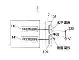
RW装置1は、図1に示すように、RW送信回路(破線)140、RW受信回路(破線)141、及びアンテナユニット3を有している。アンテナユニット3は、後述する、送信アンテナ108、及び受信アンテナ109を有している。なお、本発明における「アンテナユニット」とは、送信アンテナ及び受信アンテナが少なくとも1つずつからなる、アンテナの組み合わせをいい、複数のアンテナが一体で構成されている必要はない。 As illustrated in FIG. 1, the
RW装置1は、CPU(Central Processing Unit)102を有している。CPU102は、シンセサイザ120のデータ設定、ベースバンドフィルタ103への送信データの設定、及びレベル変換回路117からの受信データ出力の処理などを行なう。シンセサイザ120は、図12に示す無線タグ2との通信に必要な搬送波を生成する。RW装置1では、UHF帯として、例えば、850MHz〜970MHz帯を使用するが、特にこれに限る必要はなく、2.4GHz帯や400MHz帯でもよい。また、周波数ホッピングを有するシステムの場合では、シンセサイザ120で様々な周波数成分が生成される。 The
シンセサイザ120の出力の約半分の電力は、後述するアイソレータ130(第2のアイソレータ)を介して、トランジスタからなる変調器104に入力される。残りの約半分の電力は、0/90度ハイブリッド回路124を通じて受信回路のミキサ112a、112bに、受信ローカル信号として入力される。0/90度ハイブリッド回路124は、90度の位相差出力信号を発生させる電力分配器である。 About half of the output of the
ベースバンドフィルタ103でフィルタリングされた送信データは、変調器104にてシンセサイザ120により生成された搬送波で変調される。変調出力は、後段の送信アンプ105で線形動作にて増幅され、さらに後段のパワーアンプ106で所定の電力レベルまで線形動作にて増幅される。増幅された変調信号は、バンドパスフィルタ107により、高調波等の不要なスプリアスが除去され、送信アンテナ108から送信信号として出力される。 The transmission data filtered by the
空間に放出された電波は、空間での伝播損失により一部のパワーが失われるが、図12に示す無線タグ2のアンテナ201で受信され、レクテナ203にて整流動作により無線タグ2内のCPU204を起動する電力が生成される。生成される電力が、CPU204を起動させる電力レベルに到達したら、変復調器202にてRW装置1からの送信信号を復調し、CPU204にてその信号を処理する。即ち、CPU204は、メモリ205にアクセスし、このメモリ205に蓄積された情報を変復調器202にてバックスキャタ変調することで、アンテナ201を通じて、RW装置1側へ応答信号を返す。 A part of the power of the radio wave emitted to the space is lost due to propagation loss in the space, but is received by the
無線タグ2からの応答信号は、RW装置1の受信アンテナ109にて受信信号として受信され、後述するアイソレータ110(第1のアイソレータ)を介して分配器111に入力される。ここで受信電力は同位相で分配され、ミキサ112a、112bに入力される。ミキサ112a、112bでは、位相差の90度の受信周波数と同じ周波数のローカル信号によりミキシングされ、ダイレクトにベースバンド信号に変換される。 The response signal from the
ベースバンド信号に変換されたI、Q信号成分は、図1に示すように、フィルタ113a、113bにより不要な周波数成分が除去される。その後、受信アンプ114a、114bにより、ベースバンド信号の電力が所要のレベルまで増幅される。増幅されたベースバンド信号は、合成回路115によりアナログ的に同位相で合成される。合成されたベースバンドデータは、微分回路116を介してレベル変換回路117に入力され、レベル変換回路117により2値化され、CPU102にて受信データの処理が行われる。入出力インターフェース制御部101は、図示しない例えば外部PC(Personal Computer)から、制御信号などが入力される。 As shown in FIG. 1, unnecessary frequency components are removed from the I and Q signal components converted into baseband signals by
次いで、以下に本発明の実施の形態の詳細動作に関し説明する。まず、送信受信回路のアイソレーション特性改善のためのRW装置1のアンテナ構成に関し詳述する。 Next, the detailed operation of the embodiment of the present invention will be described below. First, the antenna configuration of the
図2は、水平偏波及び垂直偏波を用いたアンテナユニットの動作を示した説明図を示している。アンテナユニット3は、既に述べたように、送信アンテナ108、及び受信アンテナ109を有している。なお、RW送信回路140、及びRW受信回路141の構成は、図1で説明したものと同一であるので、これ以後、その説明は省略する。 FIG. 2 is an explanatory diagram showing the operation of the antenna unit using horizontal polarization and vertical polarization. As described above, the
このアンテナユニット3では、図2に示すように、送信アンテナ108の偏波方向が水平偏波(第1の偏波方向)、受信アンテナ109の偏波方向が垂直偏波(第2の偏波方向)に設定されている。即ち、送信アンテナ108及び受信アンテナ109は、互いの偏波方向が直交するように配置されている。既に述べたように、送信アンテナ108が送信信号を送信すると、その信号を受けた無線タグ2は応答信号を返し、受信アンテナ109が応答信号を受信信号として受信する。 In this
このように、送受信される信号の偏波方向が互いに直交するので、送受信アンテナ108、109間のアイソレーション特性を向上させることで、互いの信号を干渉させないようにすることが出来る。その結果、通信エラーの発生を抑制することが出来るので、通信切れが起きないようにすることが出来る。特に、無線タグとの通信では、送信と受信とをほぼ同時に行う必要があるため、RW装置には好適である。 As described above, since the polarization directions of the transmitted and received signals are orthogonal to each other, it is possible to prevent the mutual signals from interfering with each other by improving the isolation characteristics between the transmitting and receiving
また、アンテナユニット3の偏波方向が直線偏波である場合、後述する円偏波に比べて、アンテナユニットを小型に構成することが出来るので、RW装置1の構成を簡易にすることが出来る。 Further, when the polarization direction of the
なお、送受信アンテナ108、109の偏波方向を逆にしてもよい。即ち、送信アンテナ108の偏波方向を垂直偏波に、受信アンテナ109の偏波方向を水平偏波に設定することも可能である。また、送信アンテナと受信アンテナで、偏波方向が異なれば、必ずしも水平偏波及び垂直偏波の組み合わせである必要はないが、2つの偏波方向が直角(直交)から鋭角になると(あるいは直角から鈍角になると)、アイソレーションが劣化する。従って、2つの偏波方向は、アイソレーションが許容出来る範囲で、異なるように設定されることが望ましい。 Note that the polarization directions of the transmitting and receiving
図3は、偏波方向の変形例であって円偏波を用いたアンテナユニットの動作を示した説明図を示している。このアンテナユニット3では、図3に示すように、送信アンテナ108の偏波方向が右旋偏波(第1の偏波方向)、受信アンテナ109の偏波方向が左旋偏波(第2の偏波方向)に設定されている。即ち、送信アンテナ108及び受信アンテナ109は、互いの偏波方向が逆方向に旋回するように配置されている。 FIG. 3 is an explanatory diagram showing the operation of the antenna unit using a circular polarization as a modification of the polarization direction. In this
このように、アンテナユニット3の偏波方向が円偏波である場合も、上述した直線偏波と同様に、互いの信号を干渉させないようにすることが出来、通信エラーの発生を抑制することが出来るので、通信切れが起きないようにすることが出来る。 As described above, even when the polarization direction of the
しかも、円偏波では、直線偏波のように偏波面のずれによって通信不能とはならないので、アンテナユニット3に対する無線タグ2の向きが変化しても(つまり偏波面がずれても)、通信エラーを発生させることなく、通信を行うことが出来る。なお、送受信アンテナ108、109の偏波方向を逆にしてもよい。即ち、送信アンテナ108の偏波方向を左旋偏波に、受信アンテナ109の偏波方向を右旋偏波に設定することも可能である。また、この円偏波は楕円偏波にすることも可能である。 Moreover, in the case of circularly polarized waves, communication is not disabled due to a shift in the polarization plane as in the case of linear polarization. Therefore, even if the orientation of the
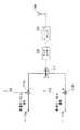
次いで、単一のRW装置にてゲートアンテナを構成した変形例について、図4を沿って説明する。図4は、複数のアンテナユニットで構成されたゲートアンテナの動作を示した説明図を示している。 Next, a modification in which a gate antenna is configured by a single RW device will be described with reference to FIG. FIG. 4 is an explanatory diagram showing the operation of the gate antenna configured with a plurality of antenna units.
RW装置1aは、図4に示すように、アンテナユニット3aを有している。アンテナユニット3aは、2つの送信アンテナ108a1、108a2と、2つの受信アンテナ109a1、109a2と有している。 As shown in FIG. 4, the
送信アンテナ108a1の偏波方向は垂直偏波、受信アンテナ109a2の偏波方向は水平偏波に設定されており、図4上方に示すように、これら送信アンテナ108a1及び受信アンテナ109a2は、対向するように配置されることで、ゲートアンテナを構成している。 The polarization direction of the transmission antenna 108a1 is set to vertical polarization, and the polarization direction of the reception antenna 109a2 is set to horizontal polarization. As shown in the upper part of FIG. 4, the transmission antenna 108a1 and the reception antenna 109a2 are opposed to each other. The gate antenna is comprised by arrange | positioning.
また、受信アンテナ109a1の偏波方向は水平偏波、送信アンテナ108a2の偏波方向は垂直偏波に設定されており、図4下方に示すように、これら受信アンテナ109a1及び送信アンテナ108a2は、対向するように配置されることで、上述と同様に、ゲートアンテナを構成している。 Further, the polarization direction of the reception antenna 109a1 is set to horizontal polarization, and the polarization direction of the transmission antenna 108a2 is set to vertical polarization. As shown in the lower part of FIG. 4, the reception antenna 109a1 and the transmission antenna 108a2 are opposed to each other. By arranging in this manner, the gate antenna is configured in the same manner as described above.
このように構成することで、送信アンテナ108a1からの送信信号が無線タグ2に送信される際に、送信アンテナ108a1と対向する受信アンテナ109a2に対する送信信号の影響を少なくすることが出来る。同様に、送信アンテナ108a2からの送信信号が無線タグ2に送信される際に、送信アンテナ108a2と対向する受信アンテナ109a1に対する送信信号の影響を少なくすることが出来る。その結果、送信出力がそのまま受信アンテナに干渉波として入力されないようにしながら、送受信アンテナで、ゲートアンテナを構成することが出来るので、通信エラーを少なくしながら、更に受信性能を向上させることが出来る。 With this configuration, when the transmission signal from the transmission antenna 108a1 is transmitted to the
次いで、上述したアンテナユニットを利用した無線タグ読み取りシステムについて、図5に沿って説明する。図5は、ゲートアンテナを構成した無線タグ読み取りシステムの動作説明図を示している。 Next, a wireless tag reading system using the above-described antenna unit will be described with reference to FIG. FIG. 5 is a diagram for explaining the operation of the RFID tag reading system having the gate antenna.
無線タグ読み取りシステム10は、図5に示すように、複数のRW装置1b、1cを有している。RW装置1bは、送信アンテナ108b、及び受信アンテナ109bを有している。RW装置1bのアンテナユニット3bでは、送信アンテナ108bの偏波方向が垂直偏波、受信アンテナ109bの偏波方向が水平偏波に設定されている。一方、RW装置1cのアンテナユニット3cでは、送信アンテナ108cの偏波方向が垂直偏波、受信アンテナ109cの偏波方向が水平偏波に設定されている。 As shown in FIG. 5, the wireless
また、図5上方に示すように、RW装置1bにおける送信アンテナ108bと、RW装置1cにおける受信アンテナ109cとが対向するように配置されている。さらに、図5下方に示すように、RW装置1bにおける受信アンテナ109bと、RW装置1cにおける送信アンテナ108cとが対向するように配置されている。即ち、RW装置1b、1cのアンテナユニット同士は、送信アンテナと受信アンテナとが対向するように配置されている。 Further, as shown in the upper part of FIG. 5, the transmitting
こうすることで、対向するアンテナ同士は、偏波方向が異なるように設定されているので、アンテナユニットを複数配置しても、アンテナが送受信する信号が干渉しないので、RW装置の受信感度を低下させることなく、複数のRW装置からなる、無線タグ読み取りシステムを容易に構成することが出来る。 By doing so, the antennas facing each other are set so that their polarization directions are different, so even if a plurality of antenna units are arranged, the signals transmitted and received by the antennas do not interfere with each other, so the reception sensitivity of the RW device is reduced. Therefore, it is possible to easily configure a wireless tag reading system composed of a plurality of RW devices.
なお、無線タグ読み取りシステムの一例として、2つの複数のRW装置で構成された場合を示したが、アンテナユニット同士を、送信アンテナと受信アンテナとが対向するように配置するものであれば、RW装置の数は必ずしも2つである必要はなく、3つ以上であってもよい。また、対向するアンテナの偏波方向は、異なる方向であればよく、例えば、左旋偏波と右旋偏波との組み合わせでもよい。 As an example of the wireless tag reading system, the case where the wireless tag reader system is configured by two or more RW devices has been shown. However, if the antenna units are arranged so that the transmission antenna and the reception antenna face each other, the RW The number of devices is not necessarily two, but may be three or more. Further, the polarization directions of the opposing antennas may be different directions, and for example, a combination of left-handed polarization and right-handed polarization may be used.
次いで、送信受信回路のアイソレーション特性改善のために、上述したアンテナユニットの他に、アイソレータの構成に関して詳述する。 Next, in order to improve the isolation characteristics of the transmission / reception circuit, the configuration of the isolator will be described in detail in addition to the antenna unit described above.
図6は、アイソレータとしてバッファアンプを挿入した(一部抜粋)送信回路図を示している。バッファアンプ(緩衝増幅器)131は、図1に示すアイソレータ130の一例であり、図6に示すように、シンセサイザ120と変調器104との間に設けられている。従って、シンセサイザ120からの出力信号は、送信系に対して変調器104に入力される。 FIG. 6 shows a transmission circuit diagram in which a buffer amplifier is inserted as an isolator (partially extracted). A buffer amplifier (buffer amplifier) 131 is an example of the isolator 130 shown in FIG. 1, and is provided between the
この変調器104では、非常に高い電圧レベルでのON/OFF制御が行われるため、シンセサイザ120の負荷が大きく変化し、その変動により受信側のローカル信号に送信側の変調信号の負荷変動が影響する場合がある。また、送信アンプ105からのノイズが、受信側のローカル信号に影響を与える場合がある。本発明では、上述したように、アイソレータとして、バッファアンプ131が挿入されているので、送信側の負荷変動の影響やノイズが、バッファアンプ131により阻止されるので、これらの影響を受信側に与えないようにすることが出来る。 Since the
なお、図1では、変調器104を設けた場合について説明したが、RW装置1は必ずしも変調器104を有している必要はない。例えば、図11に示す従来のRW装置5のように、パワーアンプ503の電源オン/オフ制御でAM変調する場合では、アイソレータにより、パワーアンプ503からのノイズが、受信側に負荷変動の影響を与えないようにすることが出来る。 Although the case where the
なお、バッファアンプと共に、抵抗やコンデンサを利用することも可能である。図7は、変調器とバッファアンプとの間に疎結合容量回路が接続された(一部抜粋)送信回路図を示している。疎結合容量回路133は、コンデンサなどからなり、この疎結合容量回路133は、変調器104とバッファアンプ131との間に接続されている。図8は、変調器とバッファアンプとの間にアッテネータが接続された(一部抜粋)送信回路図を示している。アッテネータ135は抵抗などからなり、このアッテネータ135は、変調器104とバッファアンプ131との間に接続されている。 A resistor or a capacitor can be used together with the buffer amplifier. FIG. 7 shows a transmission circuit diagram in which a loosely coupled capacitance circuit is connected between the modulator and the buffer amplifier (partially extracted). The loosely coupled
このように、バッファアンプ131と共に、疎結合容量回路133またはアッテネータ135が挿入されているので、変調器104及びパワーアンプ503とのアイソレーションをさらに向上させることが出来、受信ローカルを安定させることが出来る。 As described above, since the loosely coupled
なお、バッファアンプ131と疎結合容量回路133との順序、バッファアンプ131とアッテネータ135との順序は逆にしても、同様の効果を得ることが出来る。また、バッファアンプ131を多段に接続することで、アイソレーションを更に向上させることが出来、同様に、疎結合容量回路133を多段に接続することで、アイソレーションを更に向上させることが出来る。 Even if the order of the
また、アイソレータは送信側だけでなく、図9に示すように受信側に設けることも可能である。図9は、受信アンテナに接続されたアイソレータとしてローノイズアンプを挿入した(一部抜粋)受信回路図を示している。 Further, the isolator can be provided not only on the transmission side but also on the reception side as shown in FIG. FIG. 9 shows a reception circuit diagram in which a low-noise amplifier is inserted as an isolator connected to the reception antenna (partially extracted).
受信アンテナ109は、図9に示すように、ローノイズアンプ136に接続されている。ローノイズアンプ136は、図1に示すアイソレータ110の一例である。ローノイズアンプ136は、疎結合容量回路137を介して分配器111に接続されている。従って、0/90度ハイブリッド回路124からの受信ローカル信号は、ローノイズアンプ136により、受信アンテナ109側に回り込まないように阻止される。 The receiving
こうすることで、ダイレクトコンバージョンを利用した場合であっても、ローノイズアンプ136が、受信ローカル信号のアンテナへの放射を抑制することが出来るので、直交復調時のDC(直流)オフセットの影響を低減させることが出来、通信エラーの発生を更に抑制することが出来る。また、疎結合容量回路137により、アンプの出力側からのハインピーダンス信号の漏れを抑制することが出来る。 In this way, even when direct conversion is used, the
なお、図10に示すように、疎結合容量回路137の代わりに、アッテネータ139を挿入することも可能であり、疎結合容量回路137と同様の効果を得ることが出来る。このアッテネータとしては、アッテネータ回路は抵抗などで構成されるパイ型アッテネータが望ましい。 As shown in FIG. 10, an
なお、本明細書における「無線タグ」とは、リーダライタ装置と近接した距離(例えば数mmから数m)で無線通信を行い、無線タグ内に格納されている識別コードなどの情報を送受信する媒体をいい、形状として、ラベル型、カード型、コイン型、スティック型、チップ型など各種のものがある。従って、この「無線タグ」の用語には、いわゆる、RFIDタグ(Radio Frequency Identificationタグ)、RFタグ(Radio Frequencyタグ)、ICタグ(Integrated Circuitタグ)、無線ICタグ、電子タグ、非接触タグが含まれる。 Note that the “wireless tag” in this specification performs wireless communication at a distance (for example, several millimeters to several meters) close to the reader / writer device, and transmits and receives information such as an identification code stored in the wireless tag. A medium is used, and there are various types of shapes such as a label type, a card type, a coin type, a stick type, and a chip type. Therefore, the term “wireless tag” includes so-called RFID tags (Radio Frequency Identification tags), RF tags (Radio Frequency tags), IC tags (Integrated Circuit tags), wireless IC tags, electronic tags, and non-contact tags. included.
本発明は、通信エラーの発生を防ぐことで、通信切れを抑制することが出来る、アンテナユニット、送受信装置、無線タグ読み取り装置、及び無線タグ読み取りシステムであって、UHF帯(300Mz帯〜3、000MHz帯)に利用することが出来る。 The present invention is an antenna unit, a transmission / reception device, a wireless tag reading device, and a wireless tag reading system that can suppress communication interruption by preventing occurrence of a communication error, and includes a UHF band (300 Mz band to 3, 000 MHz band).
1 無線タグ読み取り装置(リーダライタ装置)
3、3a、3b、3c アンテナユニット
10 無線タグ読み取りシステム
104 変調器
108、108a1、108a2、108b、108c 送信アンテナ
109、109a1、109a2、109b、109c 受信アンテナ
110、136 アイソレータ(第1のアイソレータ)
130、131 アイソレータ(第2のアイソレータ)
131、136 アンプ(バッファアンプ、ローノイズアンプ)
133、137 コンデンサ(疎結合容量回路)
135、139 抵抗(アッテネータ)1 RFID tag reader (reader / writer device)
3, 3a, 3b,
130, 131 isolator (second isolator)
131, 136 amplifiers (buffer amplifiers, low noise amplifiers)
133, 137 capacitors (loosely coupled capacitors)
135, 139 Resistance (attenuator)
Claims (12)
Translated fromJapanese第1の偏波方向の送信信号を送信する送信アンテナと、
前記第1の偏波方向と異なる第2の偏波方向の受信信号を受信する受信アンテナと備えるアンテナユニット。An antenna unit having a plurality of antennas,
A transmission antenna for transmitting a transmission signal in the first polarization direction;
An antenna unit provided with a receiving antenna that receives a reception signal in a second polarization direction different from the first polarization direction.
前記偏波方向として円偏波を用いたアンテナユニット。The antenna unit according to claim 1, wherein
An antenna unit using circular polarization as the polarization direction.
前記偏波方向として直線偏波を用いたアンテナユニット。The antenna unit according to claim 1, wherein
An antenna unit using linearly polarized waves as the polarization direction.
前記アンテナユニットの受信アンテナに接続された第1のアイソレータを備える送受信装置。The antenna unit according to claim 1, further comprising:
A transmission / reception apparatus comprising a first isolator connected to a reception antenna of the antenna unit.
前記第1のアイソレータは、アンプである送受信装置。The transmission / reception device according to claim 4,
The first isolator is a transmission / reception device that is an amplifier.
前記アンプの出力側に接続された抵抗又はコンデンサを備える送受信装置。The transmission / reception device according to claim 5, further comprising:
A transmission / reception device comprising a resistor or a capacitor connected to the output side of the amplifier.
前記アンテナユニットの送信アンテナに接続された変調器と、
前記変調器に接続された第2のアイソレータとを備える送受信装置。The antenna unit according to claim 1, further comprising:
A modulator connected to the transmitting antenna of the antenna unit;
A transmission / reception device comprising: a second isolator connected to the modulator.
前記第2のアイソレータは、アンプである送受信装置。The transmission / reception device according to claim 7,
The second isolator is a transmission / reception device that is an amplifier.
前記アンプの出力側に接続された抵抗又はコンデンサを備える送受信装置。The transmission / reception device according to claim 8, further comprising:
A transmission / reception device comprising a resistor or a capacitor connected to the output side of the amplifier.
前記送信アンテナと前記受信アンテナとを対向させる無線タグ読み取り装置。The wireless tag reader according to claim 10,
A wireless tag reader that makes the transmitting antenna and the receiving antenna face each other.
前記アンテナユニット同士を、前記送信アンテナと前記受信アンテナとが対向するように配置する無線タグ読み取りシステム。The wireless tag reader according to claim 10, comprising a plurality of devices,
A wireless tag reading system in which the antenna units are arranged so that the transmitting antenna and the receiving antenna face each other.
Priority Applications (1)
| Application Number | Priority Date | Filing Date | Title |
|---|---|---|---|
| JP2005052831AJP2006238282A (en) | 2005-02-28 | 2005-02-28 | Antenna unit, transmission / reception device, wireless tag reading device, and wireless tag reading system |
Applications Claiming Priority (1)
| Application Number | Priority Date | Filing Date | Title |
|---|---|---|---|
| JP2005052831AJP2006238282A (en) | 2005-02-28 | 2005-02-28 | Antenna unit, transmission / reception device, wireless tag reading device, and wireless tag reading system |
Publications (1)
| Publication Number | Publication Date |
|---|---|
| JP2006238282Atrue JP2006238282A (en) | 2006-09-07 |
Family
ID=37045412
Family Applications (1)
| Application Number | Title | Priority Date | Filing Date |
|---|---|---|---|
| JP2005052831AWithdrawnJP2006238282A (en) | 2005-02-28 | 2005-02-28 | Antenna unit, transmission / reception device, wireless tag reading device, and wireless tag reading system |
Country Status (1)
| Country | Link |
|---|---|
| JP (1) | JP2006238282A (en) |
Cited By (49)
| Publication number | Priority date | Publication date | Assignee | Title |
|---|---|---|---|---|
| JP2008135018A (en)* | 2006-10-31 | 2008-06-12 | Semiconductor Energy Lab Co Ltd | Semiconductor device |
| WO2011048905A1 (en)* | 2009-10-21 | 2011-04-28 | 株式会社村田製作所 | Transmitting/receiving device and wireless tag reader |
| KR101090836B1 (en)* | 2010-04-29 | 2011-12-08 | (주)필텍 | Motion sensor using a Single Circular-Polarized Antenna |
| US8336786B2 (en) | 2010-03-12 | 2012-12-25 | Murata Manufacturing Co., Ltd. | Wireless communication device and metal article |
| US8396425B2 (en) | 2006-10-31 | 2013-03-12 | Semiconductor Energy Laboratory Co., Ltd. | Semiconductor device |
| US8424769B2 (en) | 2010-07-08 | 2013-04-23 | Murata Manufacturing Co., Ltd. | Antenna and RFID device |
| US8424762B2 (en) | 2007-04-14 | 2013-04-23 | Murata Manufacturing Co., Ltd. | Wireless IC device and component for wireless IC device |
| US8544759B2 (en) | 2009-01-09 | 2013-10-01 | Murata Manufacturing., Ltd. | Wireless IC device, wireless IC module and method of manufacturing wireless IC module |
| US8590797B2 (en) | 2008-05-21 | 2013-11-26 | Murata Manufacturing Co., Ltd. | Wireless IC device |
| US8602310B2 (en) | 2010-03-03 | 2013-12-10 | Murata Manufacturing Co., Ltd. | Radio communication device and radio communication terminal |
| US8613395B2 (en) | 2011-02-28 | 2013-12-24 | Murata Manufacturing Co., Ltd. | Wireless communication device |
| US8676117B2 (en) | 2006-01-19 | 2014-03-18 | Murata Manufacturing Co., Ltd. | Wireless IC device and component for wireless IC device |
| US8690070B2 (en) | 2009-04-14 | 2014-04-08 | Murata Manufacturing Co., Ltd. | Wireless IC device component and wireless IC device |
| US8704716B2 (en) | 2009-11-20 | 2014-04-22 | Murata Manufacturing Co., Ltd. | Antenna device and mobile communication terminal |
| US8718727B2 (en) | 2009-12-24 | 2014-05-06 | Murata Manufacturing Co., Ltd. | Antenna having structure for multi-angled reception and mobile terminal including the antenna |
| US8720789B2 (en) | 2012-01-30 | 2014-05-13 | Murata Manufacturing Co., Ltd. | Wireless IC device |
| US8740093B2 (en) | 2011-04-13 | 2014-06-03 | Murata Manufacturing Co., Ltd. | Radio IC device and radio communication terminal |
| US8770489B2 (en) | 2011-07-15 | 2014-07-08 | Murata Manufacturing Co., Ltd. | Radio communication device |
| US8797148B2 (en) | 2008-03-03 | 2014-08-05 | Murata Manufacturing Co., Ltd. | Radio frequency IC device and radio communication system |
| US8797225B2 (en) | 2011-03-08 | 2014-08-05 | Murata Manufacturing Co., Ltd. | Antenna device and communication terminal apparatus |
| US8814056B2 (en) | 2011-07-19 | 2014-08-26 | Murata Manufacturing Co., Ltd. | Antenna device, RFID tag, and communication terminal apparatus |
| US8853549B2 (en) | 2009-09-30 | 2014-10-07 | Murata Manufacturing Co., Ltd. | Circuit substrate and method of manufacturing same |
| US8870077B2 (en) | 2008-08-19 | 2014-10-28 | Murata Manufacturing Co., Ltd. | Wireless IC device and method for manufacturing same |
| US8878739B2 (en) | 2011-07-14 | 2014-11-04 | Murata Manufacturing Co., Ltd. | Wireless communication device |
| US8905296B2 (en) | 2011-12-01 | 2014-12-09 | Murata Manufacturing Co., Ltd. | Wireless integrated circuit device and method of manufacturing the same |
| US8917211B2 (en) | 2008-11-17 | 2014-12-23 | Murata Manufacturing Co., Ltd. | Antenna and wireless IC device |
| US8937576B2 (en) | 2011-04-05 | 2015-01-20 | Murata Manufacturing Co., Ltd. | Wireless communication device |
| US8944335B2 (en) | 2010-09-30 | 2015-02-03 | Murata Manufacturing Co., Ltd. | Wireless IC device |
| US8976075B2 (en) | 2009-04-21 | 2015-03-10 | Murata Manufacturing Co., Ltd. | Antenna device and method of setting resonant frequency of antenna device |
| US8981906B2 (en) | 2010-08-10 | 2015-03-17 | Murata Manufacturing Co., Ltd. | Printed wiring board and wireless communication system |
| US8991713B2 (en) | 2011-01-14 | 2015-03-31 | Murata Manufacturing Co., Ltd. | RFID chip package and RFID tag |
| US9024837B2 (en) | 2010-03-31 | 2015-05-05 | Murata Manufacturing Co., Ltd. | Antenna and wireless communication device |
| US9024725B2 (en) | 2009-11-04 | 2015-05-05 | Murata Manufacturing Co., Ltd. | Communication terminal and information processing system |
| US9104950B2 (en) | 2009-01-30 | 2015-08-11 | Murata Manufacturing Co., Ltd. | Antenna and wireless IC device |
| US9117157B2 (en) | 2009-10-02 | 2015-08-25 | Murata Manufacturing Co., Ltd. | Wireless IC device and electromagnetic coupling module |
| US9166291B2 (en) | 2010-10-12 | 2015-10-20 | Murata Manufacturing Co., Ltd. | Antenna device and communication terminal apparatus |
| US9165239B2 (en) | 2006-04-26 | 2015-10-20 | Murata Manufacturing Co., Ltd. | Electromagnetic-coupling-module-attached article |
| US9236651B2 (en) | 2010-10-21 | 2016-01-12 | Murata Manufacturing Co., Ltd. | Communication terminal device |
| US9281873B2 (en) | 2008-05-26 | 2016-03-08 | Murata Manufacturing Co., Ltd. | Wireless IC device system and method of determining authenticity of wireless IC device |
| US9378452B2 (en) | 2011-05-16 | 2016-06-28 | Murata Manufacturing Co., Ltd. | Radio IC device |
| US9460320B2 (en) | 2009-10-27 | 2016-10-04 | Murata Manufacturing Co., Ltd. | Transceiver and radio frequency identification tag reader |
| US9460376B2 (en) | 2007-07-18 | 2016-10-04 | Murata Manufacturing Co., Ltd. | Radio IC device |
| US9543642B2 (en) | 2011-09-09 | 2017-01-10 | Murata Manufacturing Co., Ltd. | Antenna device and wireless device |
| US9558384B2 (en) | 2010-07-28 | 2017-01-31 | Murata Manufacturing Co., Ltd. | Antenna apparatus and communication terminal instrument |
| US9692128B2 (en) | 2012-02-24 | 2017-06-27 | Murata Manufacturing Co., Ltd. | Antenna device and wireless communication device |
| US9727765B2 (en) | 2010-03-24 | 2017-08-08 | Murata Manufacturing Co., Ltd. | RFID system including a reader/writer and RFID tag |
| US9761923B2 (en) | 2011-01-05 | 2017-09-12 | Murata Manufacturing Co., Ltd. | Wireless communication device |
| US10013650B2 (en) | 2010-03-03 | 2018-07-03 | Murata Manufacturing Co., Ltd. | Wireless communication module and wireless communication device |
| US10235544B2 (en) | 2012-04-13 | 2019-03-19 | Murata Manufacturing Co., Ltd. | Inspection method and inspection device for RFID tag |
- 2005
- 2005-02-28JPJP2005052831Apatent/JP2006238282A/ennot_activeWithdrawn
Cited By (61)
| Publication number | Priority date | Publication date | Assignee | Title |
|---|---|---|---|---|
| US8725071B2 (en) | 2006-01-19 | 2014-05-13 | Murata Manufacturing Co., Ltd. | Wireless IC device and component for wireless IC device |
| US8676117B2 (en) | 2006-01-19 | 2014-03-18 | Murata Manufacturing Co., Ltd. | Wireless IC device and component for wireless IC device |
| US9165239B2 (en) | 2006-04-26 | 2015-10-20 | Murata Manufacturing Co., Ltd. | Electromagnetic-coupling-module-attached article |
| US9362984B2 (en) | 2006-10-31 | 2016-06-07 | Semiconductor Energy Laboratory Co., Ltd. | Semiconductor device |
| JP2008135018A (en)* | 2006-10-31 | 2008-06-12 | Semiconductor Energy Lab Co Ltd | Semiconductor device |
| US8396425B2 (en) | 2006-10-31 | 2013-03-12 | Semiconductor Energy Laboratory Co., Ltd. | Semiconductor device |
| US8424762B2 (en) | 2007-04-14 | 2013-04-23 | Murata Manufacturing Co., Ltd. | Wireless IC device and component for wireless IC device |
| US8662403B2 (en) | 2007-07-04 | 2014-03-04 | Murata Manufacturing Co., Ltd. | Wireless IC device and component for wireless IC device |
| US9460376B2 (en) | 2007-07-18 | 2016-10-04 | Murata Manufacturing Co., Ltd. | Radio IC device |
| US9830552B2 (en) | 2007-07-18 | 2017-11-28 | Murata Manufacturing Co., Ltd. | Radio IC device |
| US8797148B2 (en) | 2008-03-03 | 2014-08-05 | Murata Manufacturing Co., Ltd. | Radio frequency IC device and radio communication system |
| US8590797B2 (en) | 2008-05-21 | 2013-11-26 | Murata Manufacturing Co., Ltd. | Wireless IC device |
| US8973841B2 (en) | 2008-05-21 | 2015-03-10 | Murata Manufacturing Co., Ltd. | Wireless IC device |
| US9022295B2 (en) | 2008-05-21 | 2015-05-05 | Murata Manufacturing Co., Ltd. | Wireless IC device |
| US9281873B2 (en) | 2008-05-26 | 2016-03-08 | Murata Manufacturing Co., Ltd. | Wireless IC device system and method of determining authenticity of wireless IC device |
| US8870077B2 (en) | 2008-08-19 | 2014-10-28 | Murata Manufacturing Co., Ltd. | Wireless IC device and method for manufacturing same |
| US8917211B2 (en) | 2008-11-17 | 2014-12-23 | Murata Manufacturing Co., Ltd. | Antenna and wireless IC device |
| US8544759B2 (en) | 2009-01-09 | 2013-10-01 | Murata Manufacturing., Ltd. | Wireless IC device, wireless IC module and method of manufacturing wireless IC module |
| US9104950B2 (en) | 2009-01-30 | 2015-08-11 | Murata Manufacturing Co., Ltd. | Antenna and wireless IC device |
| US8690070B2 (en) | 2009-04-14 | 2014-04-08 | Murata Manufacturing Co., Ltd. | Wireless IC device component and wireless IC device |
| US8876010B2 (en) | 2009-04-14 | 2014-11-04 | Murata Manufacturing Co., Ltd | Wireless IC device component and wireless IC device |
| US9203157B2 (en) | 2009-04-21 | 2015-12-01 | Murata Manufacturing Co., Ltd. | Antenna device and method of setting resonant frequency of antenna device |
| US9564678B2 (en) | 2009-04-21 | 2017-02-07 | Murata Manufacturing Co., Ltd. | Antenna device and method of setting resonant frequency of antenna device |
| US8976075B2 (en) | 2009-04-21 | 2015-03-10 | Murata Manufacturing Co., Ltd. | Antenna device and method of setting resonant frequency of antenna device |
| US8853549B2 (en) | 2009-09-30 | 2014-10-07 | Murata Manufacturing Co., Ltd. | Circuit substrate and method of manufacturing same |
| US9117157B2 (en) | 2009-10-02 | 2015-08-25 | Murata Manufacturing Co., Ltd. | Wireless IC device and electromagnetic coupling module |
| WO2011048905A1 (en)* | 2009-10-21 | 2011-04-28 | 株式会社村田製作所 | Transmitting/receiving device and wireless tag reader |
| US9460320B2 (en) | 2009-10-27 | 2016-10-04 | Murata Manufacturing Co., Ltd. | Transceiver and radio frequency identification tag reader |
| US9024725B2 (en) | 2009-11-04 | 2015-05-05 | Murata Manufacturing Co., Ltd. | Communication terminal and information processing system |
| US8704716B2 (en) | 2009-11-20 | 2014-04-22 | Murata Manufacturing Co., Ltd. | Antenna device and mobile communication terminal |
| US8718727B2 (en) | 2009-12-24 | 2014-05-06 | Murata Manufacturing Co., Ltd. | Antenna having structure for multi-angled reception and mobile terminal including the antenna |
| US10013650B2 (en) | 2010-03-03 | 2018-07-03 | Murata Manufacturing Co., Ltd. | Wireless communication module and wireless communication device |
| US8602310B2 (en) | 2010-03-03 | 2013-12-10 | Murata Manufacturing Co., Ltd. | Radio communication device and radio communication terminal |
| US8528829B2 (en) | 2010-03-12 | 2013-09-10 | Murata Manufacturing Co., Ltd. | Wireless communication device and metal article |
| US8336786B2 (en) | 2010-03-12 | 2012-12-25 | Murata Manufacturing Co., Ltd. | Wireless communication device and metal article |
| US9727765B2 (en) | 2010-03-24 | 2017-08-08 | Murata Manufacturing Co., Ltd. | RFID system including a reader/writer and RFID tag |
| US9024837B2 (en) | 2010-03-31 | 2015-05-05 | Murata Manufacturing Co., Ltd. | Antenna and wireless communication device |
| KR101090836B1 (en)* | 2010-04-29 | 2011-12-08 | (주)필텍 | Motion sensor using a Single Circular-Polarized Antenna |
| US8424769B2 (en) | 2010-07-08 | 2013-04-23 | Murata Manufacturing Co., Ltd. | Antenna and RFID device |
| US9558384B2 (en) | 2010-07-28 | 2017-01-31 | Murata Manufacturing Co., Ltd. | Antenna apparatus and communication terminal instrument |
| US8981906B2 (en) | 2010-08-10 | 2015-03-17 | Murata Manufacturing Co., Ltd. | Printed wiring board and wireless communication system |
| US8944335B2 (en) | 2010-09-30 | 2015-02-03 | Murata Manufacturing Co., Ltd. | Wireless IC device |
| US9166291B2 (en) | 2010-10-12 | 2015-10-20 | Murata Manufacturing Co., Ltd. | Antenna device and communication terminal apparatus |
| US9236651B2 (en) | 2010-10-21 | 2016-01-12 | Murata Manufacturing Co., Ltd. | Communication terminal device |
| US9761923B2 (en) | 2011-01-05 | 2017-09-12 | Murata Manufacturing Co., Ltd. | Wireless communication device |
| US8991713B2 (en) | 2011-01-14 | 2015-03-31 | Murata Manufacturing Co., Ltd. | RFID chip package and RFID tag |
| US8613395B2 (en) | 2011-02-28 | 2013-12-24 | Murata Manufacturing Co., Ltd. | Wireless communication device |
| US8757502B2 (en) | 2011-02-28 | 2014-06-24 | Murata Manufacturing Co., Ltd. | Wireless communication device |
| US8960561B2 (en) | 2011-02-28 | 2015-02-24 | Murata Manufacturing Co., Ltd. | Wireless communication device |
| US8797225B2 (en) | 2011-03-08 | 2014-08-05 | Murata Manufacturing Co., Ltd. | Antenna device and communication terminal apparatus |
| US8937576B2 (en) | 2011-04-05 | 2015-01-20 | Murata Manufacturing Co., Ltd. | Wireless communication device |
| US8740093B2 (en) | 2011-04-13 | 2014-06-03 | Murata Manufacturing Co., Ltd. | Radio IC device and radio communication terminal |
| US9378452B2 (en) | 2011-05-16 | 2016-06-28 | Murata Manufacturing Co., Ltd. | Radio IC device |
| US8878739B2 (en) | 2011-07-14 | 2014-11-04 | Murata Manufacturing Co., Ltd. | Wireless communication device |
| US8770489B2 (en) | 2011-07-15 | 2014-07-08 | Murata Manufacturing Co., Ltd. | Radio communication device |
| US8814056B2 (en) | 2011-07-19 | 2014-08-26 | Murata Manufacturing Co., Ltd. | Antenna device, RFID tag, and communication terminal apparatus |
| US9543642B2 (en) | 2011-09-09 | 2017-01-10 | Murata Manufacturing Co., Ltd. | Antenna device and wireless device |
| US8905296B2 (en) | 2011-12-01 | 2014-12-09 | Murata Manufacturing Co., Ltd. | Wireless integrated circuit device and method of manufacturing the same |
| US8720789B2 (en) | 2012-01-30 | 2014-05-13 | Murata Manufacturing Co., Ltd. | Wireless IC device |
| US9692128B2 (en) | 2012-02-24 | 2017-06-27 | Murata Manufacturing Co., Ltd. | Antenna device and wireless communication device |
| US10235544B2 (en) | 2012-04-13 | 2019-03-19 | Murata Manufacturing Co., Ltd. | Inspection method and inspection device for RFID tag |
Similar Documents
| Publication | Publication Date | Title |
|---|---|---|
| JP2006238282A (en) | Antenna unit, transmission / reception device, wireless tag reading device, and wireless tag reading system | |
| US7761115B2 (en) | Multiple mode RF transceiver and antenna structure | |
| US9087281B2 (en) | Dual-frequency RFID tag with isolated inputs | |
| US8914061B2 (en) | Contactless integrated circuit having NFC and UHF operating modes | |
| US7155172B2 (en) | RFID receiver apparatus and method | |
| US8120464B2 (en) | RFID reader and method for removing a transmission carrier leakage signal | |
| JP5316638B2 (en) | Antenna device | |
| US9408015B2 (en) | Reducing receiver performance degradation due to frequency coexistence | |
| JP2006295729A (en) | RFID tag and antenna arrangement method | |
| CN104426574A (en) | Integrated circuit for communication | |
| US9430683B1 (en) | Passive self-jammer cancellation in RFID systems | |
| WO2007056157A3 (en) | Low return loss rugged rfid antenna | |
| KR20050013970A (en) | Antenna apparatus used commonly for 2 frequencies | |
| US9094255B2 (en) | Method and device for amplitude modulation of an electromagnetic signal emitted by a contactless transceiver system | |
| US10284240B2 (en) | Receiving circuit and wireless communication device | |
| KR100988813B1 (en) | Multi Mode RFID Reader Structure | |
| JP4637774B2 (en) | Mobile communication terminal | |
| JP2006262055A (en) | Antenna module and portable information terminal provided with the same | |
| US8659396B2 (en) | Method and apparatus for dynamically-tuned communication with one among myriad tags | |
| You et al. | Implementation of low‐cost UHF RFID reader front‐ends with carrier leakage suppression circuit | |
| JP2008263295A (en) | Wireless communication terminal device and RFID module | |
| CN106919964B (en) | A UHF RFID reader and method for adaptive phase-shifting network | |
| CN210222762U (en) | Ultrahigh frequency RFID reader-writer and ultrahigh frequency RFID reading-writing system | |
| JP5053310B2 (en) | Transceiver circuit and signal receiving method thereof | |
| KR100737855B1 (en) | Single Side Band Response Method of Wireless Identification Tag |
Legal Events
| Date | Code | Title | Description |
|---|---|---|---|
| A621 | Written request for application examination | Free format text:JAPANESE INTERMEDIATE CODE: A621 Effective date:20080214 | |
| RD01 | Notification of change of attorney | Free format text:JAPANESE INTERMEDIATE CODE: A7421 Effective date:20080312 | |
| A761 | Written withdrawal of application | Free format text:JAPANESE INTERMEDIATE CODE: A761 Effective date:20090615 |