JP2006237478A - Method and apparatus for forming boron nitride film - Google Patents
Method and apparatus for forming boron nitride filmDownload PDFInfo
- Publication number
- JP2006237478A JP2006237478AJP2005053179AJP2005053179AJP2006237478AJP 2006237478 AJP2006237478 AJP 2006237478AJP 2005053179 AJP2005053179 AJP 2005053179AJP 2005053179 AJP2005053179 AJP 2005053179AJP 2006237478 AJP2006237478 AJP 2006237478A
- Authority
- JP
- Japan
- Prior art keywords
- boron nitride
- nitride film
- film
- forming
- gas
- Prior art date
- Legal status (The legal status is an assumption and is not a legal conclusion. Google has not performed a legal analysis and makes no representation as to the accuracy of the status listed.)
- Granted
Links
- PZNSFCLAULLKQX-UHFFFAOYSA-NBoron nitrideChemical compoundN#BPZNSFCLAULLKQX-UHFFFAOYSA-N0.000titleclaimsabstractdescription151
- 229910052582BNInorganic materials0.000titleclaimsabstractdescription150
- 238000000034methodMethods0.000titleclaimsabstractdescription70
- 230000015572biosynthetic processEffects0.000claimsabstractdescription44
- 239000000758substrateSubstances0.000claimsabstractdescription42
- 238000000992sputter etchingMethods0.000claimsabstractdescription38
- QGZKDVFQNNGYKY-UHFFFAOYSA-NAmmoniaChemical compoundNQGZKDVFQNNGYKY-UHFFFAOYSA-N0.000claimsabstractdescription26
- 239000007789gasSubstances0.000claimsdescription69
- UFHFLCQGNIYNRP-UHFFFAOYSA-NHydrogenChemical compound[H][H]UFHFLCQGNIYNRP-UHFFFAOYSA-N0.000claimsdescription26
- 230000008021depositionEffects0.000claimsdescription19
- 239000001257hydrogenSubstances0.000claimsdescription15
- 229910052739hydrogenInorganic materials0.000claimsdescription15
- IJGRMHOSHXDMSA-UHFFFAOYSA-NAtomic nitrogenChemical compoundN#NIJGRMHOSHXDMSA-UHFFFAOYSA-N0.000claimsdescription14
- 239000011261inert gasSubstances0.000claimsdescription10
- BLRPTPMANUNPDV-UHFFFAOYSA-NSilaneChemical compound[SiH4]BLRPTPMANUNPDV-UHFFFAOYSA-N0.000claimsdescription9
- 229910000077silaneInorganic materials0.000claimsdescription9
- 229910052581Si3N4Inorganic materials0.000claimsdescription8
- 229910052757nitrogenInorganic materials0.000claimsdescription8
- HQVNEWCFYHHQES-UHFFFAOYSA-Nsilicon nitrideChemical compoundN12[Si]34N5[Si]62N3[Si]51N64HQVNEWCFYHHQES-UHFFFAOYSA-N0.000claimsdescription8
- BSYNRYMUTXBXSQ-UHFFFAOYSA-NAspirinChemical compoundCC(=O)OC1=CC=CC=C1C(O)=OBSYNRYMUTXBXSQ-UHFFFAOYSA-N0.000claimsdescription7
- 230000001939inductive effectEffects0.000claimsdescription5
- 238000004381surface treatmentMethods0.000claimsdescription5
- 239000010408filmSubstances0.000abstractdescription214
- 230000001965increasing effectEffects0.000abstractdescription17
- 239000010409thin filmSubstances0.000abstractdescription5
- 239000013078crystalSubstances0.000description11
- 230000004888barrier functionEffects0.000description7
- 239000000126substanceSubstances0.000description5
- XKRFYHLGVUSROY-UHFFFAOYSA-NArgonChemical compound[Ar]XKRFYHLGVUSROY-UHFFFAOYSA-N0.000description4
- 241000894007speciesSpecies0.000description4
- XLYOFNOQVPJJNP-UHFFFAOYSA-NwaterSubstancesOXLYOFNOQVPJJNP-UHFFFAOYSA-N0.000description4
- 229910052796boronInorganic materials0.000description3
- 230000007423decreaseEffects0.000description3
- 239000011229interlayerSubstances0.000description3
- 230000001681protective effectEffects0.000description3
- ZOXJGFHDIHLPTG-UHFFFAOYSA-NBoronChemical compound[B]ZOXJGFHDIHLPTG-UHFFFAOYSA-N0.000description2
- RYGMFSIKBFXOCR-UHFFFAOYSA-NCopperChemical compound[Cu]RYGMFSIKBFXOCR-UHFFFAOYSA-N0.000description2
- 229910021529ammoniaInorganic materials0.000description2
- 229910052786argonInorganic materials0.000description2
- 239000011248coating agentSubstances0.000description2
- 238000000576coating methodMethods0.000description2
- 238000007796conventional methodMethods0.000description2
- 229910052802copperInorganic materials0.000description2
- 239000010949copperSubstances0.000description2
- 238000009792diffusion processMethods0.000description2
- 238000007865dilutingMethods0.000description2
- 150000002431hydrogenChemical class0.000description2
- 229910052743kryptonInorganic materials0.000description2
- DNNSSWSSYDEUBZ-UHFFFAOYSA-Nkrypton atomChemical compound[Kr]DNNSSWSSYDEUBZ-UHFFFAOYSA-N0.000description2
- 229910052754neonInorganic materials0.000description2
- GKAOGPIIYCISHV-UHFFFAOYSA-Nneon atomChemical compound[Ne]GKAOGPIIYCISHV-UHFFFAOYSA-N0.000description2
- 229910052724xenonInorganic materials0.000description2
- FHNFHKCVQCLJFQ-UHFFFAOYSA-Nxenon atomChemical compound[Xe]FHNFHKCVQCLJFQ-UHFFFAOYSA-N0.000description2
- 235000011299Brassica oleracea var botrytisNutrition0.000description1
- 240000003259Brassica oleracea var. botrytisSpecies0.000description1
- 229910003697SiBNInorganic materials0.000description1
- 125000004429atomChemical group0.000description1
- ZOCHARZZJNPSEU-UHFFFAOYSA-NdiboronChemical compoundB#BZOCHARZZJNPSEU-UHFFFAOYSA-N0.000description1
- 230000000694effectsEffects0.000description1
- 238000005530etchingMethods0.000description1
- 239000001307heliumSubstances0.000description1
- 229910052734heliumInorganic materials0.000description1
- SWQJXJOGLNCZEY-UHFFFAOYSA-Nhelium atomChemical compound[He]SWQJXJOGLNCZEY-UHFFFAOYSA-N0.000description1
- 239000000463materialSubstances0.000description1
- 239000012528membraneSubstances0.000description1
- 238000012858packaging processMethods0.000description1
- 230000002093peripheral effectEffects0.000description1
- 238000005498polishingMethods0.000description1
- 230000002250progressing effectEffects0.000description1
- 239000004065semiconductorSubstances0.000description1
- 238000001179sorption measurementMethods0.000description1
Images


Landscapes
- Chemical Vapour Deposition (AREA)
- Formation Of Insulating Films (AREA)
Abstract
Description
Translated fromJapanese本発明は、窒化ホウ素膜の成膜方法及び成膜装置に関する。 The present invention relates to a method and apparatus for forming a boron nitride film.
LSIの微細化の進行に伴い、配線プロセスにおいて、層間絶縁膜の低誘電率化が求められている。例えば、有機塗布膜による層間絶縁膜では、誘電率を低下するため、多孔質な(ポーラス)構造としている。ところが、このようなポーラス構造の膜は、低誘電性には優れるが、機械的強度が弱いという大きな課題がある。特に、65nmノードになると、ポーラス構造の膜では、膜自体のヤング率や硬さ等が低く、機械的強度が不足するため、後工程におけるCMP(Chemical Mechanical Polishing)プロセスやパッケージ工程に耐えられないという問題が生じる。加えて、有機塗布膜等の有機系膜は、下地との密着性の問題も有るため、銅拡散バリア性等も備えた他の材料、例えば、窒化ホウ素(BN)膜による絶縁膜の開発も進んでいる。 With the progress of miniaturization of LSIs, the dielectric constant of the interlayer insulating film is required in the wiring process. For example, an interlayer insulating film made of an organic coating film has a porous structure in order to reduce the dielectric constant. However, a film having such a porous structure is excellent in low dielectric property, but has a big problem that mechanical strength is weak. In particular, at a 65 nm node, a porous structure film has a low Young's modulus, hardness, etc., and lacks mechanical strength, and therefore cannot withstand a CMP (Chemical Mechanical Polishing) process or a packaging process in a subsequent process. The problem arises. In addition, since an organic film such as an organic coating film has a problem of adhesion to a base, other materials having a copper diffusion barrier property such as a boron nitride (BN) film have also been developed. Progressing.
窒化ホウ素膜は、低誘電率を有する絶縁膜(所謂、Low−k膜)として、又、拡散バリア性を有するバリア膜(銅配線の保護膜)として、適用が検討されており、窒化ホウ素自体は機械的強度が高いものであるため、低誘電率性、バリア性、機械的強度等を全て満足できるものとして期待されている。 Boron nitride films have been studied for application as insulating films having a low dielectric constant (so-called low-k films) and as barrier films having diffusion barrier properties (protective films for copper wiring). Is expected to satisfy all of the low dielectric constant, barrier property, mechanical strength, and the like because of its high mechanical strength.
ところが、従来の成膜方法では、窒化ホウ素が六方晶結晶構造(h−BN)に成長し、その結晶構造に起因して、空隙が非常に大きい板状(カリフラワ状)の状態の薄膜となるため、機械的強度が悪く、絶縁膜やバリア膜としての機能を十分果たせないものであった。つまり、窒化ホウ素膜においても、機械的強度に関して問題があり、より緻密に成膜することが望まれている。 However, in the conventional film-forming method, boron nitride grows into a hexagonal crystal structure (h-BN), and due to the crystal structure, a thin film having a plate-like (kali-flower-like) state with very large voids is obtained. Therefore, the mechanical strength is poor, and the function as an insulating film or a barrier film cannot be sufficiently performed. That is, the boron nitride film also has a problem with respect to mechanical strength, and it is desired to form the film more densely.
本発明は上記課題に鑑みなされたもので、緻密にして、機械的強度を上げた窒化ホウ素膜の成膜方法及び成膜装置を提供することを目的とする。 The present invention has been made in view of the above problems, and an object of the present invention is to provide a method and apparatus for forming a boron nitride film that is dense and has increased mechanical strength.
上記課題を解決する第1の発明に係る窒化ホウ素膜の成膜方法は、
成膜室内にジボランガスとアンモニアガスを導入し、
前記成膜室内にプラズマを発生させて、ジボランガスとアンモニアガスとを反応させ、
スパッタエッチング作用が発生可能な電力を下限とし、実質的な成膜が該スパッタエッチング作用により停止されない電力を上限として、前記成膜室内に配置された基板に対して、バイアス電力を印加して、
前記基板に窒化ホウ素膜を成膜することを特徴とする。A method for forming a boron nitride film according to the first invention for solving the above-described problems is as follows.
Introduce diborane gas and ammonia gas into the deposition chamber,
Plasma is generated in the film forming chamber to react diborane gas and ammonia gas,
Applying a bias power to the substrate disposed in the film forming chamber, with the lower limit of the power that can generate the sputter etching action and the upper limit of the electric power at which the substantial film formation is not stopped by the sputter etching action,
A boron nitride film is formed on the substrate.
上記課題を解決する第2の発明に係る窒化ホウ素膜の成膜方法は、
第1の発明に記載の窒化ホウ素膜の成膜方法において、
前記成膜室の圧力を10mTorrより高真空にして、該窒化ホウ素膜の成膜を行うことを特徴とする。A method for forming a boron nitride film according to a second invention for solving the above-described problems is as follows.
In the method for forming a boron nitride film according to the first invention,
The boron nitride film is formed by setting the pressure in the film forming chamber to a vacuum higher than 10 mTorr.
上記課題を解決する第3の発明に係る窒化ホウ素膜の成膜方法は、
第1の発明に記載の窒化ホウ素膜の成膜方法において、
前記プラズマを3kWより高い電力で発生させて、該窒化ホウ素膜の成膜を行うことを特徴とする。A method for forming a boron nitride film according to a third aspect of the present invention for solving the above problem is as follows.
In the method for forming a boron nitride film according to the first invention,
The plasma is generated at a power higher than 3 kW to form the boron nitride film.
上記課題を解決する第4の発明に係る窒化ホウ素膜の成膜方法は、
第1の発明に記載の窒化ホウ素膜の成膜方法において、
窒素より質量の大きい不活性ガスを追加導入して、該窒化ホウ素膜の成膜を行うことを特徴とする。A method for forming a boron nitride film according to a fourth invention for solving the above-described problems is as follows.
In the method for forming a boron nitride film according to the first invention,
The boron nitride film is formed by additionally introducing an inert gas having a mass larger than that of nitrogen.
上記課題を解決する第5の発明に係る窒化ホウ素膜の成膜方法は、
第1〜第4の発明に記載の窒化ホウ素膜の成膜方法において、
前記ジボランガス及び前記アンモニアガスの導入を停止すると共に、前記成膜室内に水素ガスを導入し、水素プラズマを発生させて、
該水素プラズマにより、成膜された窒化ホウ素膜の表面処理を行うことを特徴とする。
つまり、窒化ホウ素膜のボンドを水素にて終端処理して、他の物質、特に、水等が吸着しないようにする。A method for forming a boron nitride film according to a fifth aspect of the present invention for solving the above problem is as follows.
In the method for forming a boron nitride film according to any one of the first to fourth inventions,
While stopping the introduction of the diborane gas and the ammonia gas, introducing hydrogen gas into the film forming chamber, generating hydrogen plasma,
A surface treatment of the formed boron nitride film is performed by the hydrogen plasma.
In other words, the boron nitride film bond is terminated with hydrogen so as not to adsorb other substances such as water.
上記課題を解決する第6の発明に係る窒化ホウ素膜の成膜方法は、
第1〜第5の発明に記載の窒化ホウ素膜の成膜方法において、
該窒化ホウ素膜の成膜終了時に、シランガスを追加導入すると共に、
成膜された窒化ホウ素膜の表面に、窒化ホウ化ケイ素膜を成膜することを特徴とする。A method for forming a boron nitride film according to a sixth aspect of the present invention for solving the above problem is as follows.
In the method for forming a boron nitride film according to any one of the first to fifth inventions,
At the end of the formation of the boron nitride film, additional silane gas is introduced,
A silicon nitride boride film is formed on the surface of the formed boron nitride film.
上記課題を解決する第7の発明に係る窒化ホウ素膜の成膜方法は、
第1〜第7の発明に記載の窒化ホウ素膜の成膜方法において、
前記プラズマは、ICP(Inductive Coupled Plasma)法、CCP(Capacitive Coupled Plasma)法、HWP(Helicon Wave Plasma)法、ECR(Electron Cyclotron Resonance)プラズマ法、SWP(Surface Wave Plasma)法のいずれか1つを用いて、発生させることを特徴とする。A method for forming a boron nitride film according to a seventh aspect of the present invention for solving the above problem is as follows.
In the method for forming a boron nitride film according to any one of the first to seventh inventions,
The plasma may be any one of ICP (Inductive Coupled Plasma), CCP (Capacitive Coupled Plasma), HWP (Helicon Wave Plasma), ECR (Electron Cyclotron Resonance), and SWP (Surface Wave Plasma). And generated.
上記課題を解決する第8の発明に係る窒化ホウ素膜の成膜装置は、
成膜室の上部に設置され、前記成膜室の内部にプラズマを発生させるプラズマ発生手段と、
前記成膜室の内部にアンモニアガスを導入する第1ガス導入手段と、
前記第1ガス導入手段より下方側に配置され、前記成膜室の内部にジボランガスを導入する第2ガス導入手段と
前記成膜室の下部に設置され、基板を保持する保持台と、
前記保持台に配置され、前記基板にバイアス電力を印加するバイアス印加手段とを有し、
前記バイアス印加手段は、スパッタエッチング作用が発生可能な電力を下限とし、実質的な成膜が該スパッタエッチング作用により停止されない電力を上限として、前記基板に対してバイアス電力を印加して、前記基板に窒化ホウ素膜を成膜することを特徴とする。An apparatus for forming a boron nitride film according to an eighth invention for solving the above-mentioned problems is as follows.
A plasma generating means installed at an upper part of the film forming chamber and generating plasma in the film forming chamber;
First gas introduction means for introducing ammonia gas into the film forming chamber;
A second gas introduction means that is disposed below the first gas introduction means and introduces diborane gas into the film formation chamber; a holding table that is installed at a lower portion of the film formation chamber and holds a substrate;
Bias application means disposed on the holding table and applying bias power to the substrate;
The bias applying means applies a bias power to the substrate with a power that can generate a sputter etching action as a lower limit and a power that does not stop substantial film formation by the sputter etching action as an upper limit. A boron nitride film is formed on the substrate.
上記課題を解決する第9の発明に係る窒化ホウ素膜の成膜装置は、
第8の発明に記載の窒化ホウ素膜の成膜装置において、
前記成膜室内の圧力を制御する圧力制御手段を備えると共に、
前記圧力制御手段は、前記成膜室の圧力を10mTorrより高真空に制御することを特徴とする。A film forming apparatus for a boron nitride film according to a ninth invention for solving the above-described problems,
In the boron nitride film deposition apparatus according to the eighth invention,
A pressure control means for controlling the pressure in the film forming chamber;
The pressure control means controls the pressure in the film forming chamber to a vacuum higher than 10 mTorr.
上記課題を解決する第10の発明に係る窒化ホウ素膜の成膜装置は、
第8の発明に記載の窒化ホウ素膜の成膜装置において、
前記プラズマ発生手段は、前記プラズマを3kWより高い電力で発生させることを特徴とする。A boron nitride film-forming apparatus according to a tenth invention for solving the above-described problems is provided.
In the boron nitride film deposition apparatus according to the eighth invention,
The plasma generating means generates the plasma with a power higher than 3 kW.
上記課題を解決する第11の発明に係る窒化ホウ素膜の成膜装置は、
第8の発明に記載の窒化ホウ素膜の成膜装置において、
前記成膜室内に窒素より質量の大きい不活性ガスを追加導入する追加導入手段を備えたことを特徴とする。A boron nitride film deposition apparatus according to an eleventh aspect of the present invention for solving the above problems is provided.
In the boron nitride film deposition apparatus according to the eighth invention,
An additional introduction means for additionally introducing an inert gas having a mass larger than nitrogen into the film forming chamber is provided.
上記課題を解決する第12の発明に係る窒化ホウ素膜の成膜装置は、
第8〜第11の発明に記載の窒化ホウ素膜の成膜装置において、
前記成膜室内に水素ガスを追加導入する追加導入手段を備え、
前記追加導入手段は、前記ジボランガス及び前記アンモニアガスの導入の停止後に、前記成膜室内に水素ガスを導入し、
前記プラズマ発生手段は、水素プラズマを発生させ、該水素プラズマにより、成膜された窒化ホウ素膜の表面処理を行うことを特徴とする。A boron nitride film deposition apparatus according to a twelfth aspect of the present invention for solving the above problems is provided.
In the boron nitride film forming apparatus according to any one of the eighth to eleventh inventions,
Provided with additional introduction means for additionally introducing hydrogen gas into the film formation chamber;
The additional introduction means introduces hydrogen gas into the film formation chamber after the introduction of the diborane gas and the ammonia gas is stopped,
The plasma generating means generates hydrogen plasma and performs surface treatment of the formed boron nitride film with the hydrogen plasma.
上記課題を解決する第13の発明に係る窒化ホウ素膜の成膜装置は、
第8〜第12の発明に記載の窒化ホウ素膜の成膜装置において、
前記成膜室内にシランガスを追加導入する追加導入手段を備え、
前記追加導入手段は、該窒化ホウ素膜の成膜終了時に、シランガスを追加導入し、
前記プラズマ発生手段は、成膜された窒化ホウ素膜の表面に、窒化ホウ化ケイ素膜を成膜することを特徴とする。A boron nitride film deposition apparatus according to a thirteenth aspect of the present invention for solving the above problems is provided.
In the boron nitride film forming apparatus according to any one of the eighth to twelfth inventions,
Comprising additional introduction means for additionally introducing silane gas into the film forming chamber;
The additional introduction means additionally introduces silane gas at the end of the formation of the boron nitride film,
The plasma generating means forms a silicon nitride boride film on the surface of the formed boron nitride film.
上記課題を解決する第14の発明に係る窒化ホウ素膜の成膜装置は、
第8〜第13の発明に記載の窒化ホウ素膜の成膜装置において、
前記プラズマ発生手段は、ICP(Inductive Coupled Plasma)法、CCP(Capacitive Coupled Plasma)法、HWP(Helicon Wave Plasma)法、ECR(Electron Cyclotron Resonance)プラズマ法、SWP(Surface Wave Plasma)法のいずれか1つから構成されることを特徴とする。A boron nitride film deposition apparatus according to a fourteenth aspect of the present invention for solving the above-described problems is provided.
In the boron nitride film forming apparatus according to any one of the eighth to thirteenth inventions,
The plasma generating means is any one of an ICP (Inductive Coupled Plasma) method, a CCP (Capacitive Coupled Plasma) method, an HWP (Helicon Wave Plasma) method, an ECR (Electron Cyclotron Resonance) plasma method, and an SWP (Surface Wave Plasma) method. It consists of two.
第1、第8の発明によれば、基板にバイアス電力を印加したので、スパッタエッチング作用により、疎な結晶構造を壊し、壊した部分に活性種を結合させることができ、緻密な、機械的強度の強い窒化ホウ素膜を成膜することができる。 According to the first and eighth inventions, since bias power is applied to the substrate, the sparse crystal structure can be broken by the sputter etching action, and the active species can be bonded to the broken portion. A strong boron nitride film can be formed.
第2、第9の発明によれば、成膜時の圧力を下げたので、活性種の持つ運動エネルギーが上がり、低いバイアス電力を印加しても、十分な機械的強度を持つ窒化ホウ素膜を成膜することができる。 According to the second and ninth inventions, since the pressure at the time of film formation is lowered, the kinetic energy of the active species is increased, and a boron nitride film having sufficient mechanical strength even when a low bias power is applied. A film can be formed.
第3、第10の発明によれば、プラズマ電力を大きくしたので、活性種の量が増加し、低いバイアス電力を印加しても、十分な機械的強度を持つ窒化ホウ素膜を成膜することができる。 According to the third and tenth inventions, since the plasma power is increased, the amount of active species increases, and a boron nitride film having sufficient mechanical strength can be formed even when a low bias power is applied. Can do.
第4、第11の発明によれば、運動エネルギーが大きい不活性ガスがスパッタエッチング作用に用いられることになり、低いバイアス電力を印加しても、十分な機械的強度を持つ窒化ホウ素膜を成膜することができる。 According to the fourth and eleventh inventions, an inert gas having a large kinetic energy is used for the sputter etching action, and a boron nitride film having sufficient mechanical strength is formed even when a low bias power is applied. Can be membrane.
第6、第12の発明によれば、窒化ホウ素膜のボンドを水素にて終端処理するので、他の物質、特に、水等が吸着しないようにして、窒化ホウ素膜の安定性が増し、比誘電率など電気特性の経時変化が少なくなる。 According to the sixth and twelfth inventions, since the bond of the boron nitride film is terminated with hydrogen, the stability of the boron nitride film is increased by preventing adsorption of other substances, particularly water, etc. Changes in electrical characteristics such as dielectric constant over time are reduced.
第6、第13の発明によれば、窒化ホウ素膜上に保護膜となる窒化ホウ化ケイ素膜を成膜したので、窒化ホウ素膜の安定性が増し、比誘電率など電気特性の経時変化が少なくなる。 According to the sixth and thirteenth inventions, since the silicon nitride boride film serving as the protective film is formed on the boron nitride film, the stability of the boron nitride film is increased, and the electrical characteristics such as the relative dielectric constant change over time. Less.
第7、第14の発明によれば、高密度プラズマを用いるので、緻密な窒化ホウ素膜をより効率的に成膜することができる。 According to the seventh and fourteenth inventions, since high-density plasma is used, a dense boron nitride film can be formed more efficiently.
本発明に係る窒化ホウ素膜の成膜装置、成膜方法を、図1〜図5を参照して説明する。 A boron nitride film forming apparatus and film forming method according to the present invention will be described with reference to FIGS.
<第1実施形態>
図1は、本発明に係る窒化ホウ素膜の成膜装置の実施形態の一例を示す概略図である。
本実施形態の窒化ホウ素膜の成膜装置は、円筒状の真空チャンバ1の内部が成膜室2として構成される。<First Embodiment>
FIG. 1 is a schematic view showing an example of an embodiment of a boron nitride film forming apparatus according to the present invention.
In the boron nitride film deposition apparatus of this embodiment, the inside of a
具体的には、図1に示すように、真空チャンバ1の上部には円板状の天井板3が設けられ、真空チャンバ1の下部には保持台4が備えられ、半導体等の基板6が保持台4の上面に保持される。天井板3の上部には、例えば、円形リング状の高周波アンテナ7が配置され、高周波アンテナ7には整合器8を介して高周波(RF)電源9が接続されている(プラズマ発生手段)。高周波アンテナ7に電力を供給することにより、電磁波が成膜室2に入射され、入射された電磁波が成膜室2内に導入されたガスをイオン化してプラズマ10を発生させる。 Specifically, as shown in FIG. 1, a disk-shaped
又、真空チャンバ1には、成膜室2内にアンモニア(NH3)ガスを導入するガスノズル11(第1ガス導入手段)が設けられており、ガスノズル11の下方側には、成膜室2内にジボラン(B2H6)含有ガスを導入するガスノズル12(第2ガス導入手段)が設けられている。ジボラン含有ガスは、水素(H2)ガスでジボランガスを希釈しており、ジボランガス濃度を5%〜20%としている。なお、ジボランガスを希釈するガスとしては、水素ガスのほかにヘリウム(He)、ネオン(Ne)、アルゴン(Ar)、クリプトン(Kr)、キセノン(Xe)等の不活性ガス等を適用することができる。Further, the
又、基板6を保持する保持台4には、アンテナ部13が設けられており、アンテナ部13には整合器14を介して低周波(LF)電源15が接続されている。低周波電源15は、高周波電源9より低い周波数をアンテナ部13に印加し、基板6にバイアス電力を印加できるようになっている(バイアス印加手段)。 The holding table 4 that holds the
本実施形態の成膜装置における窒化ホウ素膜の成膜方法の概略を説明する。
成膜室2内の保持台4に基板6を載せて保持する。圧力制御手段となる真空装置(図示せず)等により、成膜室2内を所定の圧力に調整すると共に、ガスノズル11からアンモニアガスを所定流量で導入し、ガスノズル12からジボラン含有ガスを所定流量で導入する。整合器8を介して高周波電源9から高周波アンテナ7に高周波電力(1MHz〜100MHz、1kW〜10kW)を印加することにより、成膜室2内で主にアンモニアガスが励起されてプラズマ状態となる。これは、アンモニアガスを導入するガスノズル11が高周波アンテナ7側に設けられているためである。そして、プラズマ化したアンモニアガスと水素ガスで希釈されたジボランガスとが反応し、この反応により、ガス状の窒化ホウ素と水素ガスが生成され、水素ガスが排気されて、窒化ホウ素膜の薄膜5が基板6の表面に成膜されることになる。そして、詳細は後述するが、緻密な窒化ホウ素膜を成膜するため、成膜時において、基板6に最適なバイアス電力を印可している。An outline of a method for forming a boron nitride film in the film forming apparatus of this embodiment will be described.
A
ここで、窒化ホウ素膜成膜時の主なプロセス条件を説明する。
基板6の温度は、温度制御手段となるヒータ(図示せず)等により制御されており、170℃〜450℃で制御されることが望ましい。
又、ガスノズル11からのアンモニアガスの流量、ガスノズル12からのジボラン含有ガスの流量については、ジボラン/アンモニア流量比が、0.1〜1となるように、好ましくは、流量比が0.25となるように設定する。
又、ジボランガスの流量とアンモニアガスの流量の総ガス流量は、100sccm〜1000sccmとなるように、好ましくは、100sccm〜400sccmとなるように設定する。
更に、成膜時の成膜室2内の圧力は、10mTorr以下に、好ましくは、1mTorr以下になるように設定する。Here, main process conditions at the time of forming the boron nitride film will be described.
The temperature of the
Further, regarding the flow rate of the ammonia gas from the
The total gas flow rate of the diborane gas flow rate and the ammonia gas flow rate is set to 100 sccm to 1000 sccm, preferably 100 sccm to 400 sccm.
Furthermore, the pressure in the
本実施形態の窒化ホウ素膜の成膜装置は、窒化ホウ素膜の成膜時に、基板6に最適なバイアス電力を印可している。通常、基板6にバイアス電力を印可すると、基板6側に活性種を引き寄せて、例えば、成膜速度が向上する等の効果がある。ところが、本発明においては、バイアス電力の印可による活性種のスパッタエッチング作用に着目し、適切なバイアス電力を印加することで、スパッタエッチング作用により窒化ホウ素膜の結晶構造を壊し、壊された部分に活性種を結合させることで、緻密で機械的強度の高い窒化ホウ素膜を成膜している。 The boron nitride film deposition apparatus of this embodiment applies an optimum bias power to the
ここで、窒化ホウ素膜の成膜時に、基板6に印可される最適なバイアス電力について、その基本的な考えを説明する。
上述したように、本発明においては、バイアス電力の印可による活性種のスパッタエッチング作用に着目しているので、少なくとも、スパッタエッチング作用により窒化ホウ素膜の結晶構造を壊すことができるバイアス電力が必要となる。つまり、バイアス電力の下限値としては、成膜室2内に配置された基板6に対して、成膜時に、スパッタエッチング作用が発生可能な電力(スレッシュホールド限界値)としている。逆に、バイアス電力の上限値としては、スパッタエッチング作用が過多となり、スパッタエッチングされる量が成膜される量より多くなり、実質的に成膜が行われなくなる電力、換言すれば、実質的な成膜がスパッタエッチング作用により停止されない電力(成膜限界値)としている。このような範囲のバイアス電力を印加することで、窒化ホウ素膜が緻密に成膜される。Here, the basic idea of the optimum bias power applied to the
As described above, the present invention focuses on the sputter etching action of the active species by applying the bias power. Therefore, at least a bias power that can break the crystal structure of the boron nitride film by the sputter etching action is required. Become. That is, the lower limit value of the bias power is set to a power (threshold limit value) at which a sputter etching action can be generated during film formation on the
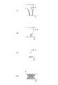
図2に、従来法における窒化ホウ素膜の成長状態(図2(a)参照)と、本発明に係る成膜方法における窒化ホウ素膜の成長状態(図2(b)〜図2(d)参照)とを示し、これらを比較して、窒化ホウ素膜の成膜時におけるバイアス電力印可によるスパッタエッチング作用を説明する。 FIG. 2 shows the growth state of the boron nitride film in the conventional method (see FIG. 2A) and the growth state of the boron nitride film in the film forming method according to the present invention (see FIGS. 2B to 2D). These are compared, and the sputter etching action by applying the bias power when the boron nitride film is formed will be described.
従来法においては、窒化ホウ素膜の成膜時に、基板6にバイアス電力を印加していなかった。このような状況下においては、図2(a)に示すように、窒化ホウ素膜は、異方性を持って、主に2次元方向(基板6に垂直な方向)に成長してしまい、空隙が非常に大きい板状(カリフラワ状)となり、疎な結晶構造となる。このような結晶構造は、特に、基板6に垂直方向に働く力に弱く、例えば、絶縁膜として成膜しても、十分な機械的強度を有するものではなかった。 In the conventional method, no bias power is applied to the
これに対して、本発明に係る成膜方法における窒化ホウ素膜は、異方性を持って成長し、疎な結晶構造に成長しても、基板6にバイアス電力を印加しているので、スパッタエッチング作用により、B、N等の活性種が上記結晶構造を壊し、壊された部分(結合手)に活性種が結合していくため(図2(b)〜図2(c)参照)、2次元ではなく、3次元方向への窒化ホウ素膜の成長を助長することになり、その結果、ポーラス度の低い、つまり、緻密で機械的強度の強い窒化ホウ素膜の薄膜5が成膜されることになる(図2(d)参照)。 On the other hand, the boron nitride film in the film forming method according to the present invention grows with anisotropy and applies a bias power to the
例えば、基板6の大きさを6インチ、基板6の温度を350℃、アンモニアガスを100sccm、ジボランガスを5sccm導入し、高周波アンテナ7に3kWの高周波電力を印加して、窒化ホウ素膜の成膜を行う場合、成膜時に印加するバイアス電力密度を、0.45W/cm2以上、2.83W/cm2未満とすると、下記表1に示すような良好な結果が得られる。For example, the size of the

補足して説明すると、印可するバイアス電力が80W未満、つまり、バイアス電力密度が0.45W/cm2未満の場合は、十分なスパッタエッチング作用が発生せず、結晶構造としては、従来と同様に疎な構造であった。そして、印可するバイアス電力を80W以上、つまり、バイアス電力密度を0.45W/cm2以上とすると、十分なスパッタエッチング作用が発生し、緻密な窒化ホウ素膜が成膜されるようになる。更に、印可するバイアス電力を500Wより大きく、つまり、バイアス電力密度を2.83W/cm2より大きくすると、スパッタエッチング作用が過多となり、成膜量よりスパッタエッチングされる量が多くなり、実質的な成膜が停止してしまう。As a supplementary explanation, when the applied bias power is less than 80 W, that is, when the bias power density is less than 0.45 W / cm2 , a sufficient sputter etching action does not occur, and the crystal structure is the same as the conventional one. It was a sparse structure. When the applied bias power is 80 W or more, that is, when the bias power density is 0.45 W / cm2 or more, a sufficient sputter etching action occurs, and a dense boron nitride film is formed. Furthermore, if the bias power to be applied is larger than 500 W, that is, if the bias power density is larger than 2.83 W / cm2 , the sputter etching action becomes excessive, and the amount of sputter etching becomes larger than the amount of film formation. Film formation stops.
本実施形態の成膜条件、つまり、基板6にバイアス電力を印加して成膜した窒化ホウ素膜の機械的強度を測定し、バイアス電力を印加しないで成膜した窒化ホウ素膜場合と比較したものが図3(a)、(b)である。なお、これらの機械的強度は、ナノインテンデーション法により計測している。図3(a)、(b)に示すように、本実施形態の成膜条件で成膜した窒化ホウ素膜の機械的強度は、硬さで約100倍、弾性率(ヤング率)で約20倍となり、又、比誘電率も、従来と同等とすることができた。 The film forming conditions of this embodiment, that is, the mechanical strength of the boron nitride film formed by applying bias power to the
上述してきたように、バイアス電力の下限値は、スパッタエッチング作用が発生可能な電力であり、バイアス電力の上限値は、実質的な成膜がスパッタエッチング作用により停止されない電力となるが、これらの上限値、下限値は、種々のプロセス条件にも左右される。そこで、実施例1〜4においては、各プロセス条件における最適なバイアス電力について説明する。 As described above, the lower limit value of the bias power is a power at which the sputter etching action can be generated, and the upper limit value of the bias power is a power at which the substantial film formation is not stopped by the sputter etching action. The upper limit value and the lower limit value also depend on various process conditions. Therefore, in Examples 1 to 4, the optimum bias power under each process condition will be described.
本実施例においては、ガスノズル11、12を用いて、成膜室2に導入する総ガス流量(アンモニアガスの流量とジボランガスの流量の和)を変化させた場合における最適なバイアス電力について言及する。 In the present embodiment, the optimum bias power when the total gas flow rate (the sum of the ammonia gas flow rate and the diborane gas flow rate) introduced into the
成膜室2に導入する総ガス流量を増やした場合、バイアス電力の下限値(スレッシュホールド限界値)は変化しないが、バイアス電力の上限値(成膜限界値)は上がる。これは、スパッタエッチング作用が発生可能な電力は総ガス流量に依存しないが、総ガス流量が増えると、成膜に寄与する活性種が増えるため、実質的な成膜がスパッタエッチング作用により停止される電力が上がるためである。従って、総ガス流量を増やすと、最適なバイアス電力の設定範囲を広くすることができ、プロセス条件の自由度が大きくなる。 When the total gas flow rate introduced into the
本実施例においては、圧力制御手段を用いて、成膜室2内の圧力を変化させた場合における最適なバイアス電力について言及する。 In this embodiment, the optimum bias power when the pressure in the
成膜室2内の圧力を高真空にした場合、バイアス電力の下限値(スレッシュホールド限界値)は下がり、バイアス電力の上限値(成膜限界値)も下がる。これは、圧力を下げる(高真空にする)と、活性種の持つ運動エネルギーが上がり、スパッタエッチング作用が発生しやすくなり、その結果、スパッタエッチング作用が発生可能な電力は下がり、又、実質的な成膜がスパッタエッチング作用により停止される電力も下がるためである。従って、圧力を下げると、最適なバイアス電力の範囲を下げることができ、低いバイアス電力でも、十分な機械的強度を持った窒化ホウ素膜を得ることができる。逆に、圧力を高くする場合、十分な機械的強度を持った窒化ホウ素膜を得るには、高いバイアス電力を印加すればよい。なお、成膜室2内の真空度としては、10mTorr以下、より好ましくは、1mTorr以下にすることが望ましい。 When the pressure in the
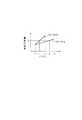
本実施例においては、高周波電源9から高周波アンテナ7に印加する高周波電力(RF)を変化させた場合における最適なバイアス電力について、図4のグラフを参照して言及する。 In this embodiment, the optimum bias power when the high frequency power (RF) applied from the high frequency power supply 9 to the
高周波アンテナ7に印加する高周波電力を大きくした場合、バイアス電力の下限値(スレッシュホールド限界値A)は変化しないが、バイアス電力の上限値(成膜限界値B→C)は下がる。これは、スパッタエッチング作用が発生可能な電力は、高周波電力に依存しないが、高周波電力を大きくすると、活性種の量が増加し、スパッタエッチング作用も大きくなり、その結果、実質的な成膜がスパッタエッチング作用により停止される電力が下がるためである。従って、同一の機械的強度Eを得たい場合、低い高周波電力(3kW)では、大きいバイアス電力Eが必要であったが、高い高周波電力(4kW)では、低いバイアス電力Fでよく、低いバイアス電力Fでも、十分な機械的強度を持った窒化ホウ素膜を得ることができる。逆に、低い高周波電力とする場合、十分な機械的強度を持った窒化ホウ素膜を得るには、高いバイアス電力を印加すればよい。なお、高周波アンテナ7に印加する高周波電力としては、3kW以上とすることが望ましい。 When the high-frequency power applied to the high-
本実施例においては、成膜室2に導入するガス種を増やした場合における最適なバイアス電力について言及する。 In this embodiment, the optimum bias power when the number of gas species introduced into the
具体的には、図1に示した成膜装置において、成膜室2内に窒素より質量の大きい不活性ガスを追加導入する追加導入手段を設けて、成膜室2に導入するガス種を増やしている。或いは、ガスノズル11、12を兼用して用いて、成膜室2に導入するガス種を増やしてもよい。追加するガス種としては、ホウ素やチッ素より質量の大きい不活性ガス、例えば、ネオン(Ne)、アルゴン(Ar)、クリプトン(Kr)、キセノン(Xe)等の希ガスが望ましく、イオン化し易く、成膜に直接影響しないものがよい。ガス種を追加した場合、バイアス電力の下限値(スレッシュホールド限界値)はさがり、バイアス電力の上限値(成膜限界値)も下がる。これは、ホウ素やチッ素より質量の大きい不活性ガスを添加すると、運動エネルギーが大きい不活性ガスがスパッタエッチング作用に用いられることになり、その結果、スパッタエッチング作用が発生可能な電力は下がり、又、実質的な成膜がスパッタエッチング作用により停止される電力も下がるためである。従って、低いバイアス電力でも、十分な機械的強度を持った窒化ホウ素膜を得ることができる。 Specifically, in the film forming apparatus shown in FIG. 1, additional introduction means for additionally introducing an inert gas having a mass larger than nitrogen is provided in the
本発明に係る成膜方法により成膜された窒化ホウ素膜は、スパッタエッチング作用により結晶構造を壊し、壊された部分に活性種を結合させて成膜を行っているため、膜中にフリーな結合手(ボンド)が残る傾向がある。このようなボンドは、他の原子、分子、特に、水等が吸着し易く、膜質の経時変化をもたらすおそれがあるため、本実施例及び実施例6においては、窒化ホウ素膜の成膜後に行うプロセスについて説明をする。 The boron nitride film formed by the film forming method according to the present invention breaks the crystal structure by the sputter etching action, and forms the film by bonding active species to the broken part. There is a tendency for bonds to remain. Such a bond is likely to adsorb other atoms and molecules, particularly water, and may cause a change in film quality over time. Therefore, in this embodiment and
本実施例においては、図1に示した成膜装置において、成膜室2内に水素ガスを追加導入する追加導入手段を設けている。或いは、成膜終了後、ガスノズル11、12を用いて、水素ガスを成膜室2に導入するようにしてもよい。 In this embodiment, the film forming apparatus shown in FIG. 1 is provided with additional introduction means for additionally introducing hydrogen gas into the
具体的なプロセスとしては、成膜終了と共に、ジボランガス及びアンモニアガスの導入を停止し、その後、成膜室2内に水素ガスを導入し、高周波アンテナ7を用いて、水素プラズマを発生させる。そして、成膜された窒化ホウ素膜を、水素プラズマにより表面処理し、窒化ホウ素膜のボンドを水素にて終端処理して、他の物質、特に、水等が吸着しないようにしている。他の物質が吸着しにくくなることにより、窒化ホウ素膜の安定性が増し、比誘電率など電気特性の経時変化が少なくなる。 As a specific process, the introduction of diborane gas and ammonia gas is stopped at the end of film formation, and then hydrogen gas is introduced into the
本実施例においては、図1に示した成膜装置において、成膜室2内にシランガス(SiH4)を追加導入する追加導入手段を設けている。或いは、ガスノズル11、12を兼用して用いて、シランガス(SiH4)を成膜室2に導入するようにしてもよい。In the present embodiment, in the film forming apparatus shown in FIG. 1, additional introducing means for additionally introducing silane gas (SiH4 ) into the
具体的なプロセスとしては、窒化ホウ素膜を所望の膜厚に成膜後、ジボランガス、アンモニアガスにシランガスを追加導入して、成膜された窒化ホウ素膜の表面に、窒化ホウ化ケイ素(SiBN)膜を成膜する。窒化ホウ化ケイ素膜は下地膜となる窒化ホウ素膜の保護膜(キャップ膜)となり、窒化ホウ素膜の安定性が増し、比誘電率など電気特性の経時変化が少なくなる。なお、実施例5において説明した水素プラズマによる表面処理を行った後、窒化ホウ素膜上に窒化ホウ化ケイ素膜の成膜を行うようにしてもよい。 As a specific process, after forming a boron nitride film to a desired film thickness, silane gas is additionally introduced into diborane gas and ammonia gas, and silicon nitride boride (SiBN) is formed on the surface of the formed boron nitride film. A film is formed. The silicon nitride boride film serves as a protective film (cap film) for the boron nitride film serving as a base film, and the stability of the boron nitride film is increased, and the change with time in electrical characteristics such as relative dielectric constant is reduced. Note that a silicon nitride boride film may be formed over the boron nitride film after the surface treatment using hydrogen plasma described in
<他の実施形態>
図5(a)〜図5(e)に、本発明に係る窒化ホウ素膜の成膜装置の他の実施形態例の概略図を示す。これらは、具体的には、プラズマ発生手段を実施形態1とは異なる構成としたものである。なお、図5(a)〜図5(e)においては、同等の構成部材に同じ符号を付している。<Other embodiments>
FIG. 5A to FIG. 5E are schematic views of other embodiments of the boron nitride film forming apparatus according to the present invention. Specifically, the plasma generating means has a configuration different from that of the first embodiment. In addition, in FIG. 5A-FIG. 5E, the same code | symbol is attached | subjected to the equivalent structural member.
例えば、図5(a)は、ICP(Inductive Coupled Plasma)法を用いて、プラズマ発生手段を構成したものである。実施形態1の窒化ホウ素膜の成膜装置のプラズマ発生手段も、ICP法を用いて構成したものであり、基本的な構成は、本実施形態の窒化ホウ素膜の成膜装置と似ている。本実施形態では、真空チャンバ21の外周側面に高周波アンテナ22を配置した点が異なっており、この高周波アンテナ22に高周波(RF)電源23が接続される。ここでも、実施形態1と同様に、基板を保持する保持台24には、低周波(LF)電源25が接続され、基板にバイアス電力が印加できるように構成されている。 For example, FIG. 5A shows a configuration in which plasma generating means is configured using an ICP (Inductive Coupled Plasma) method. The plasma generating means of the boron nitride film forming apparatus of the first embodiment is also configured using the ICP method, and the basic configuration is similar to the boron nitride film forming apparatus of the present embodiment. The present embodiment is different in that a
又、図5(b)は、CCP(Capacitive Coupled Plasma)法を用いて、プラズマ発生手段を構成したものである。これは、一般的には、平行平板型と呼ばれており、下部電極となる保持台26と、保持台26の上方に配置した上部電極27とを、真空チャンバ21内に平行に配置し、上部電極27に高周波電源23が接続されたものである。ここでも、保持台26には、低周波電源25が接続され、基板にバイアス電力が印加できるように構成されている。 FIG. 5B shows a plasma generating means using a CCP (Capacitive Coupled Plasma) method. This is generally called a parallel plate type. A holding
又、図5(c)は、ECR(Electron Cyclotron Resonance)プラズマ法を用いて、プラズマ発生手段を構成したものである。これは、マイクロ波と磁場コイル28によるECR磁界により、高密度プラズマを発生させるものである。ここでも、保持台24には、低周波電源25が接続され、基板にバイアス電力が印加できるように構成されている。 Further, FIG. 5C shows a plasma generating means using an ECR (Electron Cyclotron Resonance) plasma method. This generates high-density plasma by the ECR magnetic field generated by the microwave and the
又、図5(d)は、SWP(Surface Wave Plasma)法を用いて、プラズマ発生手段を構成したものである。これは、マイクロ波を伝播する導波管29の下面に、細い間隙を有するスロットアンテナ30を設けたものであり、マイクロ波により誘電体表面に表面波が伝播し、高密度なプラズマが生成されるものである。ここでも、保持台24には、低周波電源25が接続され、基板にバイアス電力が印加できるように構成されている。 FIG. 5 (d) shows a configuration in which plasma generating means is configured by using a SWP (Surface Wave Plasma) method. In this case, a
又、図5(e)は、HWP(Helicon Wave Plasma)法を用いて、プラズマ発生手段を構成したものである。これは、高周波電源23を接続したヘリコン波アンテナ31により、ヘリコン波を発生させると共に、磁場コイル28により磁界を発生させることにより、高密度なプラズマが生成されるものである。ここでも、保持台24には、低周波電源25が接続され、基板にバイアス電力が印加できるように構成されている。 FIG. 5E shows the plasma generating means using the HWP (Helicon Wave Plasma) method. This is because a helicon wave is generated by the
図5(a)〜図5(e)に示したような、他の実施形態の窒化ホウ素膜の成膜装置においても、上記実施例1〜6の実施が可能であり、高密度プラズマを用いることにより、緻密な窒化ホウ素膜をより効率的に成膜することができる。 In the boron nitride film deposition apparatus of other embodiments as shown in FIGS. 5A to 5E, the above-described Examples 1 to 6 can be carried out, and high-density plasma is used. Thus, a dense boron nitride film can be formed more efficiently.
本発明に係る成膜方法、成膜装置よって成膜された窒化ホウ素膜は、緻密であるため、機械的強度が高く、下地との密着性も強くなる。又、窒化ホウ素膜は、バリア化、低誘電率化が可能であり、低誘電率の層間絶縁膜やバリア膜としての適用が可能である。 Since the boron nitride film formed by the film forming method and the film forming apparatus according to the present invention is dense, the mechanical strength is high and the adhesion to the base is also strong. Further, the boron nitride film can be used as a barrier and have a low dielectric constant, and can be applied as an interlayer insulating film or a barrier film having a low dielectric constant.
1 真空チャンバ
2 成膜室
3 天井板
4 保持台
5 薄膜(窒化ホウ素膜)
6 基板
7 高周波アンテナ
8 整合器
9 高周波(RF)電源
10 プラズマ
11 ガスノズル
12 ガスノズル
13 アンテナ部
14 整合器
15 低周波(LF)電源DESCRIPTION OF
6
Claims (14)
Translated fromJapanese前記成膜室内にプラズマを発生させて、ジボランガスとアンモニアガスとを反応させ、
スパッタエッチング作用が発生可能な電力を下限とし、実質的な成膜が該スパッタエッチング作用により停止されない電力を上限として、前記成膜室内に配置された基板に対して、バイアス電力を印加して、
前記基板に窒化ホウ素膜を成膜することを特徴とする窒化ホウ素膜の成膜方法。Introduce diborane gas and ammonia gas into the deposition chamber,
Plasma is generated in the film forming chamber to react diborane gas and ammonia gas,
Applying a bias power to the substrate disposed in the film forming chamber, with the lower limit of the power that can generate the sputter etching action and the upper limit of the electric power at which the substantial film formation is not stopped by the sputter etching action,
A method for forming a boron nitride film, comprising forming a boron nitride film on the substrate.
前記成膜室の圧力を10mTorrより高真空にして、該窒化ホウ素膜の成膜を行うことを特徴とする窒化ホウ素膜の成膜方法。In the film-forming method of the boron nitride film of Claim 1,
A method of forming a boron nitride film, wherein the boron nitride film is formed by setting the pressure in the film formation chamber to a vacuum higher than 10 mTorr.
前記プラズマを3kWより高い電力で発生させて、該窒化ホウ素膜の成膜を行うことを特徴とする窒化ホウ素膜の成膜方法。In the film-forming method of the boron nitride film of Claim 1,
A method for forming a boron nitride film, wherein the plasma is generated at a power higher than 3 kW to form the boron nitride film.
窒素より質量の大きい不活性ガスを追加導入して、該窒化ホウ素膜の成膜を行うことを特徴とする窒化ホウ素膜の成膜方法。In the film-forming method of the boron nitride film of Claim 1,
A method for forming a boron nitride film, wherein an inert gas having a mass greater than that of nitrogen is additionally introduced to form the boron nitride film.
前記ジボランガス及び前記アンモニアガスの導入を停止すると共に、前記成膜室内に水素ガスを導入し、水素プラズマを発生させて、
該水素プラズマにより、成膜された窒化ホウ素膜の表面処理を行うことを特徴とする窒化ホウ素膜の成膜方法。In the film-forming method of the boron nitride film in any one of Claims 1 thru | or 4,
While stopping the introduction of the diborane gas and the ammonia gas, introducing hydrogen gas into the film forming chamber, generating hydrogen plasma,
A method for forming a boron nitride film, comprising performing surface treatment of the formed boron nitride film with the hydrogen plasma.
該窒化ホウ素膜の成膜終了時に、シランガスを追加導入すると共に、
成膜された窒化ホウ素膜の表面に、窒化ホウ化ケイ素膜を成膜することを特徴とする窒化ホウ素膜の成膜方法。In the film-forming method of the boron nitride film in any one of Claims 1 thru | or 4,
At the end of the formation of the boron nitride film, additional silane gas is introduced,
A method for forming a boron nitride film, comprising forming a silicon nitride boride film on a surface of the formed boron nitride film.
前記プラズマは、ICP(Inductive Coupled Plasma)法、CCP(Capacitive Coupled Plasma)法、HWP(Helicon Wave Plasma)法、ECR(Electron Cyclotron Resonance)プラズマ法、SWP(Surface Wave Plasma)法のいずれか1つを用いて、発生させることを特徴とする窒化ホウ素膜の成膜方法。In the film-forming method of the boron nitride film in any one of Claims 1 thru | or 6,
The plasma may be any one of ICP (Inductive Coupled Plasma), CCP (Capacitive Coupled Plasma), HWP (Helicon Wave Plasma), ECR (Electron Cyclotron Resonance), and SWP (Surface Wave Plasma). A method of forming a boron nitride film, characterized by using and generating the boron nitride film.
前記成膜室の内部にアンモニアガスを導入する第1ガス導入手段と、
前記第1ガス導入手段より下方側に配置され、前記成膜室の内部にジボランガスを導入する第2ガス導入手段と
前記成膜室の下部に設置され、基板を保持する保持台と、
前記保持台に配置され、前記基板にバイアス電力を印加するバイアス印加手段とを有し、
前記バイアス印加手段は、スパッタエッチング作用が発生可能な電力を下限とし、実質的な成膜が該スパッタエッチング作用により停止されない電力を上限として、前記基板に対してバイアス電力を印加して、前記基板に窒化ホウ素膜を成膜することを特徴とする窒化ホウ素膜の成膜装置。A plasma generating means installed at an upper part of the film forming chamber and generating plasma in the film forming chamber;
First gas introduction means for introducing ammonia gas into the film forming chamber;
A second gas introduction means that is disposed below the first gas introduction means and introduces diborane gas into the film formation chamber; a holding table that is installed at a lower portion of the film formation chamber and holds a substrate;
Bias application means disposed on the holding table and applying bias power to the substrate;
The bias applying means applies a bias power to the substrate with a power that can generate a sputter etching action as a lower limit and a power that does not stop substantial film formation by the sputter etching action as an upper limit. An apparatus for forming a boron nitride film, wherein a boron nitride film is formed on the substrate.
前記成膜室内の圧力を制御する圧力制御手段を備えると共に、
前記圧力制御手段は、前記成膜室の圧力を10mTorrより高真空に制御することを特徴とする窒化ホウ素膜の成膜装置。The boron nitride film forming apparatus according to claim 8,
A pressure control means for controlling the pressure in the film forming chamber;
The boron nitride film forming apparatus, wherein the pressure control means controls the pressure in the film forming chamber to a vacuum higher than 10 mTorr.
前記プラズマ発生手段は、前記プラズマを3kWより高い電力で発生させることを特徴とする窒化ホウ素膜の成膜装置。The boron nitride film forming apparatus according to claim 8,
The apparatus for forming a boron nitride film, wherein the plasma generating means generates the plasma with a power higher than 3 kW.
前記成膜室内に窒素より質量の大きい不活性ガスを追加導入する追加導入手段を備えたことを特徴とする窒化ホウ素膜の成膜装置。The method for forming a boron nitride film according to claim 8,
An apparatus for forming a boron nitride film, comprising additional introduction means for additionally introducing an inert gas having a mass larger than nitrogen into the film formation chamber.
前記成膜室内に水素ガスを追加導入する追加導入手段を備え、
前記追加導入手段は、前記ジボランガス及び前記アンモニアガスの導入の停止後に、前記成膜室内に水素ガスを導入し、
前記プラズマ発生手段は、水素プラズマを発生させ、該水素プラズマにより、成膜された窒化ホウ素膜の表面処理を行うことを特徴とする窒化ホウ素膜の成膜装置。The method for forming a boron nitride film according to any one of claims 8 to 11,
Provided with additional introduction means for additionally introducing hydrogen gas into the film formation chamber;
The additional introduction means introduces hydrogen gas into the film formation chamber after the introduction of the diborane gas and the ammonia gas is stopped,
The apparatus for forming a boron nitride film, wherein the plasma generating means generates hydrogen plasma and performs surface treatment of the formed boron nitride film with the hydrogen plasma.
前記成膜室内にシランガスを追加導入する追加導入手段を備え、
前記追加導入手段は、該窒化ホウ素膜の成膜終了時に、シランガスを追加導入し、
前記プラズマ発生手段は、成膜された窒化ホウ素膜の表面に、窒化ホウ化ケイ素膜を成膜することを特徴とする窒化ホウ素膜の成膜装置。The method for forming a boron nitride film according to any one of claims 8 to 11,
Comprising additional introduction means for additionally introducing silane gas into the film forming chamber;
The additional introduction means additionally introduces silane gas at the end of the formation of the boron nitride film,
An apparatus for forming a boron nitride film, wherein the plasma generating means forms a silicon nitride boride film on the surface of the formed boron nitride film.
前記プラズマ発生手段は、ICP(Inductive Coupled Plasma)法、CCP(Capacitive Coupled Plasma)法、HWP(Helicon Wave Plasma)法、ECR(Electron Cyclotron Resonance)プラズマ法、SWP(Surface Wave Plasma)法のいずれか1つから構成されることを特徴とする窒化ホウ素膜の成膜装置。In the film-forming method of the boron nitride film in any one of Claims 8 thru | or 13,
The plasma generating means is any one of an ICP (Inductive Coupled Plasma) method, a CCP (Capacitive Coupled Plasma) method, an HWP (Helicon Wave Plasma) method, an ECR (Electron Cyclotron Resonance) plasma method, and an SWP (Surface Wave Plasma) method. An apparatus for forming a boron nitride film, comprising:
Priority Applications (1)
| Application Number | Priority Date | Filing Date | Title |
|---|---|---|---|
| JP2005053179AJP4358765B2 (en) | 2005-02-28 | 2005-02-28 | Boron nitride film forming method and film forming apparatus |
Applications Claiming Priority (1)
| Application Number | Priority Date | Filing Date | Title |
|---|---|---|---|
| JP2005053179AJP4358765B2 (en) | 2005-02-28 | 2005-02-28 | Boron nitride film forming method and film forming apparatus |
Publications (2)
| Publication Number | Publication Date |
|---|---|
| JP2006237478Atrue JP2006237478A (en) | 2006-09-07 |
| JP4358765B2 JP4358765B2 (en) | 2009-11-04 |
Family
ID=37044762
Family Applications (1)
| Application Number | Title | Priority Date | Filing Date |
|---|---|---|---|
| JP2005053179AExpired - Fee RelatedJP4358765B2 (en) | 2005-02-28 | 2005-02-28 | Boron nitride film forming method and film forming apparatus |
Country Status (1)
| Country | Link |
|---|---|
| JP (1) | JP4358765B2 (en) |
Cited By (5)
| Publication number | Priority date | Publication date | Assignee | Title |
|---|---|---|---|---|
| WO2010047375A1 (en) | 2008-10-22 | 2010-04-29 | ローム株式会社 | Method for forming boron-containing thin film and multilayer structure |
| JP2018056345A (en)* | 2016-09-29 | 2018-04-05 | 東京エレクトロン株式会社 | Hard mask and manufacturing method thereof |
| KR20180069705A (en)* | 2016-12-15 | 2018-06-25 | 도쿄엘렉트론가부시키가이샤 | Film forming method, boron film, and film forming apparatus |
| KR20190113619A (en)* | 2018-03-28 | 2019-10-08 | 도쿄엘렉트론가부시키가이샤 | Boron-based film forming method and boron-based film apparatus |
| JP2019186306A (en)* | 2018-04-04 | 2019-10-24 | 東京エレクトロン株式会社 | Boron-based film deposition method and film deposition apparatus |
- 2005
- 2005-02-28JPJP2005053179Apatent/JP4358765B2/ennot_activeExpired - Fee Related
Cited By (11)
| Publication number | Priority date | Publication date | Assignee | Title |
|---|---|---|---|---|
| WO2010047375A1 (en) | 2008-10-22 | 2010-04-29 | ローム株式会社 | Method for forming boron-containing thin film and multilayer structure |
| JP2018056345A (en)* | 2016-09-29 | 2018-04-05 | 東京エレクトロン株式会社 | Hard mask and manufacturing method thereof |
| KR20180069705A (en)* | 2016-12-15 | 2018-06-25 | 도쿄엘렉트론가부시키가이샤 | Film forming method, boron film, and film forming apparatus |
| CN108220922A (en)* | 2016-12-15 | 2018-06-29 | 东京毅力科创株式会社 | Film build method, boron film and film formation device |
| US10388524B2 (en) | 2016-12-15 | 2019-08-20 | Tokyo Electron Limited | Film forming method, boron film, and film forming apparatus |
| KR102084296B1 (en)* | 2016-12-15 | 2020-03-03 | 도쿄엘렉트론가부시키가이샤 | Film forming method, boron film, and film forming apparatus |
| CN108220922B (en)* | 2016-12-15 | 2020-12-29 | 东京毅力科创株式会社 | Film formation method, boron film, and film formation apparatus |
| KR20190113619A (en)* | 2018-03-28 | 2019-10-08 | 도쿄엘렉트론가부시키가이샤 | Boron-based film forming method and boron-based film apparatus |
| KR102205227B1 (en)* | 2018-03-28 | 2021-01-19 | 도쿄엘렉트론가부시키가이샤 | Boron-based film forming method and boron-based film apparatus |
| JP2019186306A (en)* | 2018-04-04 | 2019-10-24 | 東京エレクトロン株式会社 | Boron-based film deposition method and film deposition apparatus |
| JP7049894B2 (en) | 2018-04-04 | 2022-04-07 | 東京エレクトロン株式会社 | Boron-based film film forming method and film forming equipment |
Also Published As
| Publication number | Publication date |
|---|---|
| JP4358765B2 (en) | 2009-11-04 |
Similar Documents
| Publication | Publication Date | Title |
|---|---|---|
| US9659791B2 (en) | Metal removal with reduced surface roughness | |
| TWI662617B (en) | Halogen-free gas-phase silicon etch | |
| JP4256763B2 (en) | Plasma processing method and plasma processing apparatus | |
| TW432493B (en) | Inductively coupled plasma CVD | |
| CN102956473B (en) | Rising the method for the conformal amorphous carbon film of height of deposition in feature | |
| JP2991192B1 (en) | Plasma processing method and plasma processing apparatus | |
| US10475659B2 (en) | Method of processing target object | |
| WO1998021747A1 (en) | Plasma film forming method and plasma film forming apparatus | |
| US11319630B2 (en) | Deposition apparatus and deposition method | |
| CN103620740A (en) | Selective deposition of polymer films on bare silicon instead of oxide surface | |
| JP3336975B2 (en) | Substrate processing method | |
| JP2008181710A (en) | Plasma processing apparatus and method | |
| WO2002052628A1 (en) | Plasma processing method and plasma processor | |
| US6811831B1 (en) | Method for depositing silicon nitride | |
| US20220319841A1 (en) | Deposition of low-stress carbon-containing layers | |
| JP4358765B2 (en) | Boron nitride film forming method and film forming apparatus | |
| WO2000031787A1 (en) | Dry etching device and dry etching method | |
| WO2012043250A1 (en) | Method and device for forming insulation film | |
| JP6441994B2 (en) | Method for etching a porous membrane | |
| JP4478352B2 (en) | Plasma processing apparatus, plasma processing method, and structure manufacturing method | |
| JP3530788B2 (en) | Microwave supplier, plasma processing apparatus and processing method | |
| JP2019024139A (en) | Method for etching a porous membrane | |
| TW201831723A (en) | Film Forming Method, Boron Film, and Film Forming Apparatus | |
| JP3172340B2 (en) | Plasma processing equipment | |
| US20070034601A1 (en) | Surface treating method and surface-treating apparatus |
Legal Events
| Date | Code | Title | Description |
|---|---|---|---|
| A621 | Written request for application examination | Effective date:20071107 Free format text:JAPANESE INTERMEDIATE CODE: A621 | |
| A977 | Report on retrieval | Free format text:JAPANESE INTERMEDIATE CODE: A971007 Effective date:20081226 | |
| A131 | Notification of reasons for refusal | Free format text:JAPANESE INTERMEDIATE CODE: A131 Effective date:20090106 | |
| A521 | Written amendment | Effective date:20090309 Free format text:JAPANESE INTERMEDIATE CODE: A523 | |
| A131 | Notification of reasons for refusal | Free format text:JAPANESE INTERMEDIATE CODE: A131 Effective date:20090421 | |
| A521 | Written amendment | Free format text:JAPANESE INTERMEDIATE CODE: A523 Effective date:20090622 | |
| TRDD | Decision of grant or rejection written | ||
| A01 | Written decision to grant a patent or to grant a registration (utility model) | Effective date:20090714 Free format text:JAPANESE INTERMEDIATE CODE: A01 | |
| A01 | Written decision to grant a patent or to grant a registration (utility model) | Free format text:JAPANESE INTERMEDIATE CODE: A01 | |
| A61 | First payment of annual fees (during grant procedure) | Free format text:JAPANESE INTERMEDIATE CODE: A61 Effective date:20090806 | |
| FPAY | Renewal fee payment (prs date is renewal date of database) | Year of fee payment:3 Free format text:PAYMENT UNTIL: 20120814 | |
| FPAY | Renewal fee payment (prs date is renewal date of database) | Year of fee payment:3 Free format text:PAYMENT UNTIL: 20120814 | |
| FPAY | Renewal fee payment (prs date is renewal date of database) | Free format text:PAYMENT UNTIL: 20130814 Year of fee payment:4 | |
| LAPS | Cancellation because of no payment of annual fees |