JP2006237386A - Nitride system semiconductor light emitting diode - Google Patents
Nitride system semiconductor light emitting diodeDownload PDFInfo
- Publication number
- JP2006237386A JP2006237386AJP2005051557AJP2005051557AJP2006237386AJP 2006237386 AJP2006237386 AJP 2006237386AJP 2005051557 AJP2005051557 AJP 2005051557AJP 2005051557 AJP2005051557 AJP 2005051557AJP 2006237386 AJP2006237386 AJP 2006237386A
- Authority
- JP
- Japan
- Prior art keywords
- layer
- light
- thickness
- ohmic electrode
- type
- Prior art date
- Legal status (The legal status is an assumption and is not a legal conclusion. Google has not performed a legal analysis and makes no representation as to the accuracy of the status listed.)
- Pending
Links
- 239000004065semiconductorSubstances0.000titleclaimsabstractdescription74
- 150000004767nitridesChemical class0.000titleclaimsabstractdescription60
- 229910052751metalInorganic materials0.000claimsdescription40
- 239000002184metalSubstances0.000claimsdescription40
- 239000000758substrateSubstances0.000description24
- 238000000034methodMethods0.000description22
- JMASRVWKEDWRBT-UHFFFAOYSA-NGallium nitrideChemical compound[Ga]#NJMASRVWKEDWRBT-UHFFFAOYSA-N0.000description18
- 229910004298SiO 2Inorganic materials0.000description18
- 238000005530etchingMethods0.000description16
- 238000000605extractionMethods0.000description9
- 238000005566electron beam evaporationMethods0.000description8
- 230000001681protective effectEffects0.000description7
- 238000004519manufacturing processMethods0.000description6
- 229910052763palladiumInorganic materials0.000description5
- 230000007547defectEffects0.000description4
- 238000001312dry etchingMethods0.000description4
- 229910052594sapphireInorganic materials0.000description4
- 239000010980sapphireSubstances0.000description4
- 229910052782aluminiumInorganic materials0.000description3
- 229910052737goldInorganic materials0.000description3
- -1nitride compoundChemical class0.000description3
- 230000003287optical effectEffects0.000description3
- 229910052719titaniumInorganic materials0.000description3
- 230000005540biological transmissionEffects0.000description2
- 239000013078crystalSubstances0.000description2
- 230000002950deficientEffects0.000description2
- 239000000463materialSubstances0.000description2
- 238000000206photolithographyMethods0.000description2
- 238000002834transmittanceMethods0.000description2
- 229910052984zinc sulfideInorganic materials0.000description2
- 229910002704AlGaNInorganic materials0.000description1
- 229910015363Au—SnInorganic materials0.000description1
- 229910001218Gallium arsenideInorganic materials0.000description1
- 229910002677Pd–SnInorganic materials0.000description1
- VYPSYNLAJGMNEJ-UHFFFAOYSA-NSilicium dioxideChemical compoundO=[Si]=OVYPSYNLAJGMNEJ-UHFFFAOYSA-N0.000description1
- 235000005811Viola aduncaNutrition0.000description1
- 240000009038Viola odorataSpecies0.000description1
- 235000013487Viola odorataNutrition0.000description1
- 235000002254Viola papilionaceaNutrition0.000description1
- 230000003321amplificationEffects0.000description1
- 230000015572biosynthetic processEffects0.000description1
- 238000005229chemical vapour depositionMethods0.000description1
- 239000002131composite materialSubstances0.000description1
- 229910052802copperInorganic materials0.000description1
- 230000000694effectsEffects0.000description1
- 230000005684electric fieldEffects0.000description1
- 229910052733galliumInorganic materials0.000description1
- 238000000171gas-source molecular beam epitaxyMethods0.000description1
- 238000010438heat treatmentMethods0.000description1
- 238000002248hydride vapour-phase epitaxyMethods0.000description1
- 239000012535impuritySubstances0.000description1
- 230000001678irradiating effectEffects0.000description1
- CPLXHLVBOLITMK-UHFFFAOYSA-Nmagnesium oxideInorganic materials[Mg]=OCPLXHLVBOLITMK-UHFFFAOYSA-N0.000description1
- 230000008018meltingEffects0.000description1
- 238000002844meltingMethods0.000description1
- 229910003465moissaniteInorganic materials0.000description1
- 229910052759nickelInorganic materials0.000description1
- 238000003199nucleic acid amplification methodMethods0.000description1
- 238000001579optical reflectometryMethods0.000description1
- 238000005498polishingMethods0.000description1
- 238000000926separation methodMethods0.000description1
- 229910010271silicon carbideInorganic materials0.000description1
- 229910052709silverInorganic materials0.000description1
- 229910000679solderInorganic materials0.000description1
- 239000011029spinelSubstances0.000description1
- 229910052596spinelInorganic materials0.000description1
- 238000000992sputter etchingMethods0.000description1
- WGPCGCOKHWGKJJ-UHFFFAOYSA-NsulfanylidenezincChemical compound[Zn]=SWGPCGCOKHWGKJJ-UHFFFAOYSA-N0.000description1
- 239000011800void materialSubstances0.000description1
- 229910052724xenonInorganic materials0.000description1
- FHNFHKCVQCLJFQ-UHFFFAOYSA-Nxenon atomChemical compound[Xe]FHNFHKCVQCLJFQ-UHFFFAOYSA-N0.000description1
- XLOMVQKBTHCTTD-UHFFFAOYSA-Nzinc oxideInorganic materials[Zn]=OXLOMVQKBTHCTTD-UHFFFAOYSA-N0.000description1
Images


Landscapes
- Led Devices (AREA)
Abstract
Description
Translated fromJapanese本発明は、窒化物系半導体発光ダイオードに関する。 The present invention relates to a nitride semiconductor light emitting diode.
近年、GaN、InN、AlN等の窒化物系化合物半導体は、青色や緑色の発光ダイオード(LED)や青紫色半導体レーザなどの発光素子、高温動作可能な高速トランジスタなどの電子デバイスの材料として盛んに用いられている。 In recent years, nitride compound semiconductors such as GaN, InN, and AlN have been actively used as materials for electronic devices such as light emitting elements such as blue and green light emitting diodes (LEDs) and blue-violet semiconductor lasers, and high-speed transistors that can operate at high temperatures. It is used.
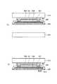
発光ダイオードの構造としては、例えば、図12及び図13に示すような構造が挙げられる。 Examples of the structure of the light emitting diode include structures shown in FIGS. 12 and 13.
図12に示す発光ダイオードの構造は、以下のように形成される。サファイア基板601の主面に、n型GaN層602、活性層603、p型GaN層604をMOCVD(Metal Organic Chemical Vapor Deposition)法などによって形成した後、例えば、CF4ガスを用いたRIE(Reactive Ion Etching)によって、n型GaN層602が露出する所望の深さにメサエッチングを施す。次に、p型GaN層604上に、例えば、Ni、Pd、Auの順に形成されてなる光透過性p型オーミック電極606をフォトリソグラフ技術とリフトオフ技術などによって選択的に形成し、SiO2からなる誘電体層607をその全面に形成する。次に、誘電体層607の一部をフォトリソグラフ技術と選択エッチング技術によって開孔し、光透過性p型オーミック電極606上の誘電体層開孔部における電極表面から、例えば、Ti、Pd、Auの順に形成されてなるp型パッド電極611を形成する。一方、n型GaN層602上の誘電体層開孔部における電極表面から、例えば、Al、Ti、Pd、Auの順に形成されてなるn型オーミック電極及びn型パッド電極613を形成する。図12に示す構造によると、活性層603で発光した光を、主にp型GaN層604側から外部(矢印F方向)へ取り出す発光ダイオードとなる。The structure of the light emitting diode shown in FIG. 12 is formed as follows. After an n-
一方、図13に示す発光ダイオードの構造は、以下のように形成される。n型GaN基板701の主面に、n型GaN層702、活性層703、p型GaN層704をMOCVD法などによって形成した後、例えば、CF4ガスを用いたRIEによって、n型GaN層702が露出する所望の深さにメサエッチングを施す。次に、p型GaN層704上に、例えば、Al、Ag、Tiの順に形成されてなる光反射性p型オーミック電極719をフォトリソグラフ技術とリフトオフ技術などによって選択的に形成し、SiO2からなる誘電体層707をその全面に形成する。次に、誘電体層707の一部をフォトリソグラフ技術と選択エッチング技術によって選択的に開孔し、光反射性p型オーミック電極719上の誘電体層開孔部における電極表面から、例えば、Ti、Pd、Auの順に形成されてなるp型パッド電極711を形成する。一方、n型GaN基板701上に、例えば、Al、Ti、Pd、Auの順に形成されてなるn型オーミック電極及びn型パッド電極713を形成する。図13に示す構造によると、活性層703で発光した光を光反射性p型オーミック電極719で反射して、主にn型GaN基板701側から外部(矢印G方向)へ取り出す発光ダイオードとなる。On the other hand, the structure of the light emitting diode shown in FIG. 13 is formed as follows. After an n-
又、活性層で発光した光を、主にn型電極で反射してp型半導体側から外部に取り出す発光ダイオード構造も開示されている(例えば、特許文献1参照。)。この発光ダイオードは、n型半導体層に誘電体層を形成し、その一部を開孔し、かかる誘電体層と一部露出したn型半導体層全面にn型オーミック電極とn型パッド電極をそれぞれ形成する構造である。
しかしながら、図12に示す構造の場合、光透過性p型オーミック電極606の透過率は、発光波長が480nmの場合、約60%程度であり、発光波長が400nmの場合、約45%程度である。このように、光透過性p型オーミック電極606を透過させて光を取り出す場合、光取り出し効率が悪く、発光ダイオードの高光度化が困難である。 However, in the case of the structure shown in FIG. 12, the transmittance of the light transmissive p-
又、図13に示す構造の場合、光反射性p型オーミック電極719の反射率は、発光波長が480nmの場合、約80%程度であり、発光波長が400nmの場合、約70%程度である。このように、光反射性p型オーミック電極719で反射させて光を取り出す場合、図12に示す構造に比べると、光取り出し効率は改善される。しかしながら、例えば、GaN半導体の場合には、欠陥密度が1×10⁶〜1010/cm2程度であることから、欠陥による電気ショート特性を示すものが極端に増大し、ウェハ内でのチップ歩留まりが、例えば5%以下を示す場合も生じる。In the case of the structure shown in FIG. 13, the reflectance of the light-reflective p-
更に、特許文献1に示す構造の場合、p型GaNなどp型半導体層の不純物濃度が1×10¹⁸/cm3以下と低い場合には、電界広がりがほとんどないため、活性層での発光は、p型オーミック電極面積に依存する。このため、光取り出し効率はあまり改善されないこととなる。Furthermore, in the case of the structure shown in Patent Document 1, when the impurity concentration of the p-type semiconductor layer such as p-type GaN is as low as 1 × 10¹⁸ / cm3 or less, there is almost no electric field spread, and thus light emission in the active layer is not caused. , Depending on the p-type ohmic electrode area. For this reason, the light extraction efficiency is not improved so much.
そこで、本発明は、上記の課題に鑑み、ウェハ内でのチップ歩留まりを改善するとともに、光取り出し効率の更なる向上を実現する窒化物系半導体発光ダイオードを提供することを目的とする。 In view of the above problems, an object of the present invention is to provide a nitride-based semiconductor light-emitting diode that improves chip yield in a wafer and further improves light extraction efficiency.
上記目的を達成するため、本発明の特徴は、(a)活性層を含む窒化物系半導体素子層上に形成された光透過性オーミック電極と、(b)光透過性オーミック電極上に形成された誘電体層と、(c)誘電体層上に形成された光反射金属層とを備える窒化物系半導体発光ダイオードであることを要旨とする。 In order to achieve the above object, the present invention is characterized in that (a) a light-transmitting ohmic electrode formed on a nitride-based semiconductor element layer including an active layer, and (b) a light-transmitting ohmic electrode. The gist of the present invention is a nitride-based semiconductor light-emitting diode comprising a dielectric layer and (c) a light-reflecting metal layer formed on the dielectric layer.
本発明の特徴に係る窒化物系半導体発光ダイオードによると、光透過性オーミック電極を備えるため、ウェハ内でのチップ歩留まりを改善するとともに、誘電体層内で光干渉現象を生じるために、特定の波長領域のピークを有した光が外部に放出され、光取り出し効率の更なる向上を実現することができる。 According to the nitride-based semiconductor light emitting diode according to the feature of the present invention, since the light-transmitting ohmic electrode is provided, the chip yield in the wafer is improved and a light interference phenomenon is generated in the dielectric layer. Light having a peak in the wavelength region is emitted to the outside, and further improvement in light extraction efficiency can be realized.
又、本発明の特徴に係る窒化物系半導体発光ダイオードにおいて、誘電体層は部分的に開孔し、光透過性オーミック電極と光反射金属層とは、当該開孔した部分で接触することが好ましい。 In the nitride semiconductor light emitting diode according to the feature of the present invention, the dielectric layer may be partially opened, and the light-transmitting ohmic electrode and the light reflecting metal layer may be in contact with each other at the opened portion. preferable.
この窒化物系半導体発光ダイオードによると、光透過性オーミック電極と光反射金属層とが電気的に接続され、全面に広がる電極を形成することができる。 According to this nitride-based semiconductor light-emitting diode, the light-transmitting ohmic electrode and the light-reflecting metal layer are electrically connected to form an electrode that extends over the entire surface.
又、本発明の特徴に係る窒化物系半導体発光ダイオードにおいて、光透過性オーミック電極及び誘電体層は、取り出す光の波長に応じた所定の膜厚を有することが好ましい。 In the nitride semiconductor light emitting diode according to the features of the present invention, it is preferable that the light transmissive ohmic electrode and the dielectric layer have a predetermined film thickness according to the wavelength of the light to be extracted.
この窒化物系半導体発光ダイオードによると、光透過性オーミック電極と誘電体層との膜厚を調整することで、外部に放出される特定波長のピークを調整することができる。 According to this nitride-based semiconductor light-emitting diode, the peak of a specific wavelength emitted to the outside can be adjusted by adjusting the film thickness of the light-transmitting ohmic electrode and the dielectric layer.
本発明によると、ウェハ内でのチップ歩留まりを改善するとともに、光取り出し効率の更なる向上を実現する窒化物系半導体発光ダイオードを提供することができる。 According to the present invention, it is possible to provide a nitride-based semiconductor light-emitting diode that improves chip yield in a wafer and further improves light extraction efficiency.
次に、図面を参照して、本発明の第1〜第4の実施の形態を説明する。以下の図面の記載において、同一又は類似の部分には、同一又は類似の符号を付している。ただし、図面は模式的なものであり、各寸法の比率等は現実のものとは異なることに留意すべきである。従って、具体的な寸法等は以下の説明を参酌して判断すべきものである。又、図面相互間においても互いの寸法の関係や比率が異なる部分が含まれていることは勿論である。 Next, first to fourth embodiments of the present invention will be described with reference to the drawings. In the following description of the drawings, the same or similar parts are denoted by the same or similar reference numerals. However, it should be noted that the drawings are schematic and ratios of dimensions and the like are different from actual ones. Accordingly, specific dimensions and the like should be determined in consideration of the following description. Moreover, it is a matter of course that portions having different dimensional relationships and ratios are included between the drawings.
本発明の第1〜第4の実施の形態に係る窒化物系半導体発光ダイオードは、活性層を含む窒化物系半導体素子層上に形成された光透過性p型オーミック電極と、光透過性p型オーミック電極上に形成された誘電体層と、誘電体層上に形成された光反射金属層とを備える。即ち、窒化物系半導体素子層上から、光透過性p型オーミック電極、誘電体層、光反射金属層が順に形成される構造である。 The nitride-based semiconductor light-emitting diodes according to the first to fourth embodiments of the present invention include a light-transmitting p-type ohmic electrode formed on a nitride-based semiconductor element layer including an active layer, and a light-transmitting p. A dielectric layer formed on the type ohmic electrode, and a light reflecting metal layer formed on the dielectric layer. In other words, the light-transmitting p-type ohmic electrode, the dielectric layer, and the light-reflecting metal layer are sequentially formed on the nitride-based semiconductor element layer.
まず、本発明に係る窒化物系半導体発光ダイオードのサンプル構造として、図1に、基板401上に、光透過性オーミック電極406、誘電体層407、光反射金属層409が順に形成された構造を示す。 First, as a sample structure of a nitride-based semiconductor light emitting diode according to the present invention, a structure in which a light-transmitting ohmic electrode 406, a
具体的には、石英ガラスからなる基板401上に、約2nmの厚みを有するPd層と、約4nmの厚みを有するAu層と、約1nmの厚みを有するNi層とからなる光透過性オーミック電極406を、順次形成する。次に、光透過性オーミック電極406上に、厚み300nmのSiO2からなる誘電体層407を形成する。次に、誘電体層407上に、約1nmの厚みを有するTi層と、約200nmの厚みを有するAg層と、約1nmの厚みを有するTi層とからなる光反射金属層409を、順次形成する。Specifically, a light-transmitting ohmic electrode comprising a Pd layer having a thickness of about 2 nm, an Au layer having a thickness of about 4 nm, and a Ni layer having a thickness of about 1 nm on a
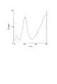
こうして形成されたサンプル構造に、キセノンランプ光源からの光を基板401側から入射(矢印A方向)し、光反射金属層409で反射して、再び基板401側から外部に取り出された(矢印B方向)光の強度を測定した結果を図2に示す。図2より、波長480nmにおける反射率が約90%となり、極めて高い反射率が得られている。 Light from the xenon lamp light source is incident on the sample structure thus formed from the
又、上記と同じ構造で、光透過性オーミック電極406上に、厚み380nmのSiO2からなる誘電体層407を形成し、同様の光を入射して、反射した光の強度を測定した結果を図3に示す。図3より、波長400nmにおける反射率が約85%となり、極めて高い反射率が得られている。In addition, a
(第1の実施の形態)
次に、第1の実施の形態に係る窒化物系半導体発光ダイオードについて、図4を用いて説明する。(First embodiment)
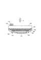
Next, the nitride semiconductor light emitting diode according to the first embodiment will be described with reference to FIG.
図4に示す窒化物系半導体発光ダイオードは、n型GaN基板101の主面に、n型GaN層102、活性層103、p型GaN層104を備える。p型GaN層104上には、約2nmの厚みを有するPd層と、約4nmの厚みを有するAu層と、約1nmの厚みを有するNi層とからなる光透過性p型オーミック電極106を備える。又、光透過性p型オーミック電極106上には、その全面に、厚み380nmのSiO2からなる誘電体層107を備え、誘電体層107上には、約1nmの厚みを有するTi層と、約200nmの厚みを有するAg層とからなる光反射金属層109を備える。このとき、光透過性p型オーミック電極106及び誘電体層107は、取り出す光の波長に応じた所定の膜厚を有する。又、誘電体層107の一部は、選択エッチングにより開孔され、光透過性p型オーミック電極106と光反射金属層109とは、電気的機械的に接触する。The nitride semiconductor light emitting diode shown in FIG. 4 includes an n-
又、光反射金属層109上には、SiO2からなる保護膜110と、保護膜110の一部を開孔して形成された、約10nmの厚みを有するTi層と、約100nmの厚みを有するPd層と、約300nmの厚みを有するAu層とからなるp型パッド電極111とを備える。一方、n型GaN基板101の他方の主面上には、約2nmの厚みを有するAl層と、約10nmの厚みを有するPd層とからなるn型オーミック電極112と、約10nmの厚みを有するTi層と、約10nmの厚みを有するPd層と、約300nmの厚みを有するAu層とからなるn型パッド電極113を備える。Further, a
図4に示す構造によると、活性層103で発光し、光透過性p型オーミック電極106を透過した光が、光反射金属層109で反射して、主にn型GaN基板101側から外部(矢印C方向)へ取り出す紫外発光ダイオードとなる。 According to the structure shown in FIG. 4, light emitted from the
次に、図4に示す窒化物系半導体発光ダイオードの製造方法について、図5及び図6を用いて説明する。 Next, a method for manufacturing the nitride-based semiconductor light-emitting diode shown in FIG. 4 will be described with reference to FIGS.
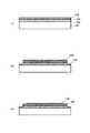
まず、図5(a)に示すように、MOCVD法を用いて、n型GaN基板101上に、n型GaN層102、活性層103、p型GaN層104を順次成長させる。 First, as shown in FIG. 5A, an n-
次に、図5(b)に示すように、選択的にパターニングしたSiO2膜をマスク層105とし、例えば、Cl2ガスを用いたドライエッチング技術によって、n型GaN層102が露出する所望の深さにメサエッチングを施す。このようにして、n型GaN層102の一部を露出させる。そして、マスク層105を除去する。Next, as shown in FIG. 5B, the SiO2 film that is selectively patterned is used as a
次に、図5(c)に示すように、電子ビーム蒸着により、p型GaN層104上に、約2nmの厚みを有するPd層と、約4nmの厚みを有するAu層と、約1nmの厚みを有するNi層とからなる光透過性p型オーミック電極106を形成する。尚、光透過性p型オーミック電極106の膜厚は、取り出す光の波長に応じて変化させることとする。 Next, as shown in FIG. 5C, a Pd layer having a thickness of about 2 nm, an Au layer having a thickness of about 4 nm, and a thickness of about 1 nm are formed on the p-
次に、図6(a)に示すように、電子ビーム蒸着により、光透過性p型オーミック電極106の全面に、厚み380nmのSiO2からなる誘電体層107を形成する。尚、誘電体層107の膜厚は、取り出す光の波長に応じて変化させることとする。そして、フォトリソグラフ技術及び選択エッチングによって、光透過性p型オーミック電極106の一部を開孔し、開孔部108を形成する。Next, as shown in FIG. 6A, a
次に、図6(b)に示すように、電子ビーム蒸着により、誘電体層107上に、約1nmの厚みを有するTi層と、約200nmの厚みを有するAg層とからなる光反射金属層109を形成する。このとき、光透過性p型オーミック電極106と光反射金属層109とは、開孔部108において、電気的機械的に接触する。又、光反射金属層109上に、電子ビーム蒸着により、SiO2からなる保護膜110を形成する。そして、フォトリソグラフ技術及び選択エッチングによって、保護膜110の一部を開孔し、約10nmの厚みを有するTi層と、約100nmの厚みを有するPd層と、約300nmの厚みを有するAu層とからなるp型パッド電極111を形成する。Next, as shown in FIG. 6B, a light-reflecting metal layer comprising a Ti layer having a thickness of about 1 nm and an Ag layer having a thickness of about 200 nm on the
次に、図6(c)に示すように、n型GaN基板101を約100μm程度の厚さに整形し、n型GaN基板101の他方の主面上に、約2nmの厚みを有するAl層と、約10nmの厚みを有するPd層とからなるn型オーミック電極112と、約10nmの厚みを有するTi層と、約10nmの厚みを有するPd層と、約300nmの厚みを有するAu層とからなるn型パッド電極113を形成する。 Next, as shown in FIG. 6C, the n-
(第2の実施の形態)
次に、第2の実施の形態に係る他の窒化物系半導体発光ダイオードについて、図7を用いて説明する。(Second Embodiment)
Next, another nitride semiconductor light emitting diode according to the second embodiment will be described with reference to FIG.
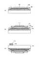
図7に示す窒化物系半導体発光ダイオードは、サファイア基板201の主面に、n型GaN層202、活性層203、p型GaN層204を備える。又、活性層203及びp型GaN層204の一部は、ドライエッチング技術によりエッチングされ、n型GaN層202が露出する。又、p型GaN層204上には、約2nmの厚みを有するPd層と、約4nmの厚みを有するAu層と、約1nmの厚みを有するNi層とからなる光透過性p型オーミック電極206を備える。又、光透過性p型オーミック電極206上には、その全面に、厚み300nmのSiO2からなる誘電体層207を備え、誘電体層207上には、約1nmの厚みを有するTi層と、約200nmの厚みを有するAg層とからなる光反射金属層209を備える。このとき、光透過性p型オーミック電極206及び誘電体層207は、取り出す光の波長に応じた所定の膜厚を有する。又、誘電体層207の一部は、選択エッチングにより開孔され、光透過性p型オーミック電極206と光反射金属層209とは、電気的機械的に接触する。The nitride semiconductor light emitting diode shown in FIG. 7 includes an n-
又、光反射金属層209上には、SiO2からなる保護膜210と、保護膜210の一部を開孔して形成された、約10nmの厚みを有するTi層と、約100nmの厚みを有するPd層と、約300nmの厚みを有するAu層とからなるp型パッド電極211とを備える。一方、エッチングによって、n型GaN層202が露出した面には、約10nmの厚みを有するAl層と、約5nmの厚みを有するTi層と、約10nmの厚みを有するPd層と、約300nmの厚みを有するAu層とからなるn型オーミック電極212及びn型パッド電極213を備える。On the light reflecting
図7に示す構造によると、活性層203で発光し、光透過性p型オーミック電極206を透過した光が、光反射金属層209で反射して、主にサファイア基板201側から外部(矢印D方向)へ取り出す青色発光ダイオードとなる。 According to the structure shown in FIG. 7, light emitted from the
(第3の実施の形態)
次に、第3の実施の形態に係る更に他の窒化物系半導体発光ダイオードについて、図8を用いて説明する。(Third embodiment)
Next, still another nitride semiconductor light emitting diode according to the third embodiment will be described with reference to FIG.
図8に示す窒化物系半導体発光ダイオードは、n型GaN基板301の主面に、n型GaN層302、活性層303、p型GaN層304を備える。又、p型GaN層304上には、約2nmの厚みを有するPd層と、約4nmの厚みを有するAu層と、約1nmの厚みを有するNi層とからなる光透過性p型オーミック電極306を備える。又、光透過性p型オーミック電極306上には、その全面に、厚み300nmのSiO2からなる誘電体層317を備え、誘電体層317の一部は開孔され、光透過性p型オーミック電極306上に、約10nmの厚みを有するAl層と、約5nmの厚みを有するTi層と、約10nmの厚みを有するPd層と、約300nmの厚みを有するAu層とからなるp型パッド電極311を備える。The nitride semiconductor light emitting diode shown in FIG. 8 includes an n-
一方、n型GaN基板301の他方の主面上には、その全面に、約2nmの厚みを有するAl層と、約10nmの厚みを有するPd層とからなる光透過性n型オーミック電極316を備える。又、光透過性n型オーミック電極316上には、その全面に、厚み380nmのSiO2からなる誘電体層307を備え、誘電体層307上には、約1nmの厚みを有するTi層と、約200nmの厚みを有するAg層とからなる光反射金属層309を備える。このとき、光透過性n型オーミック電極316及び誘電体層307は、取り出す光の波長に応じた所定の膜厚を有する。又、誘電体層307の一部は、選択エッチングにより開孔され、光透過性n型オーミック電極316と光反射金属層309とは、電気的機械的に接触する。On the other hand, on the other main surface of the n-
又、光反射金属層309上には、約10nmの厚みを有するTi層と、約100nmの厚みを有するPd層と、約300nmの厚みを有するAu層とからなるn型パッド電極313とを備える。 Further, an n-
図8に示す構造によると、活性層303で発光し、光透過性p型オーミック電極306を透過した光と誘電体層317を透過した光が矢印E方向へ取り出されると共に、光透過性n型オーミック電極316と誘電体層317とを透過して光反射金属層309で効率良く反射した光も、矢印E方向へ取り出すことのできる紫外発光ダイオードとなる。 According to the structure shown in FIG. 8, the light emitted from the
(第4の実施の形態)
次に、第4の実施の形態に係る窒化物系半導体発光ダイオードについて、図9を用いて説明する。(Fourth embodiment)
Next, a nitride semiconductor light emitting diode according to a fourth embodiment will be described with reference to FIG.
第4の実施の形態では、成長用基板上に成長した窒化物系半導体素子層上に支持基板を貼り付け、窒化物系半導体素子層から成長用基板を分離することによって製造される窒化物系半導体発光ダイオードについて、説明する。 In the fourth embodiment, a nitride substrate manufactured by attaching a support substrate on a nitride-based semiconductor element layer grown on a growth substrate and separating the growth substrate from the nitride-based semiconductor element layer. The semiconductor light emitting diode will be described.
図9に示す窒化物系半導体発光ダイオードは、n型GaN層502上に、活性層503、p型GaN層504を備える。p型GaN層504上には、約2nmの厚みを有するPd層と、約4nmの厚みを有するAu層と、約1nmの厚みを有するNi層とからなる光透過性p型オーミック電極506を備える。又、光透過性p型オーミック電極506上には、その全面に、厚み380nmのSiO2からなる誘電体層507を備え、誘電体層507上には、約1nmの厚みを有するTi層と、約200nmの厚みを有するAg層とからなる光反射金属層509を備える。このとき、光透過性p型オーミック電極506及び誘電体層507は、取り出す光の波長に応じた所定の膜厚を有する。又、誘電体層507の一部は、選択エッチングにより開孔され、光透過性p型オーミック電極506と光反射金属層509とは、電気的機械的に接触する。The nitride semiconductor light emitting diode shown in FIG. 9 includes an
又、光反射金属層509上には、約10nmの厚みを有するTi層と、約100nmの厚みを有するPd層と、約300nmの厚みを有するAu層とからなるp型パッド電極511とを備える。一方、n型GaN層502の他方の主面上には、約2nmの厚みを有するAl層と、約10nmの厚みを有するPd層とからなるn型オーミック電極と、約10nmの厚みを有するTi層と、約10nmの厚みを有するPd層と、約300nmの厚みを有するAu層とからなるn型パッド電極513を備える。 Further, a p-
図9に示す構造によると、活性層503で発光し、光透過性p型オーミック電極506を透過した光が、光反射金属層509で反射して、主にn型GaN基板501側から外部へ取り出す紫外発光ダイオードとなる。 According to the structure shown in FIG. 9, the light emitted from the
次に、図9に示す窒化物系半導体発光ダイオードの製造方法について、図10及び図11を用いて説明する。 Next, a method for manufacturing the nitride-based semiconductor light-emitting diode shown in FIG. 9 will be described with reference to FIGS.
まず、図10(a)に示すように、MOCVD法を用いて、n型GaN基板501上に、n型GaN層502、活性層503、p型GaN層504を順次成長させる。次に、選択的にパターニングしたSiO2膜をマスク層とし、例えば、Cl2ガスを用いたドライエッチング技術によって、n型GaN層502が露出する所望の深さにメサエッチングを施す。このようにして、n型GaN層502の一部を露出させる。そして、マスク層を除去する。次に、電子ビーム蒸着により、p型GaN層504上に、約2nmの厚みを有するPd層と、約4nmの厚みを有するAu層と、約1nmの厚みを有するNi層とからなる光透過性p型オーミック電極506を形成する。尚、光透過性p型オーミック電極506の膜厚は、取り出す光の波長に応じて変化させることとする。First, as shown in FIG. 10A, an n-
次に、電子ビーム蒸着により、光透過性p型オーミック電極506の全面に、厚み380nmのSiO2からなる誘電体層507を形成する。尚、誘電体層507の膜厚は、取り出す光の波長に応じて変化させることとする。そして、フォトリソグラフ技術及び選択エッチングによって、光透過性p型オーミック電極506の一部を開孔する。次に、電子ビーム蒸着により、誘電体層507上に、約1nmの厚みを有するTi層と、約200nmの厚みを有するAg層とからなる光反射金属層509を形成する。このとき、光透過性p型オーミック電極506と光反射金属層509とは、開孔部において、電気的機械的に接触する。又、光反射金属層509上に、電子ビーム蒸着により、約10nmの厚みを有するTi層と、約100nmの厚みを有するPd層と、約300nmの厚みを有するAu層とからなるp型パッド電極511を形成する。Next, a
次に、図10(b)に示すように、例えば、Cu:50重量%、Cu2O:50重量%の含有率を有する複合材料からなる支持基板118を準備し、図10(c)に示すように、p型パッド電極511と、支持基板118とを、Au−SnやPd−Sn、In−Pdなどからなる半田、あるいはAgからなる導電性ペーストを介して、熱圧着する。Next, as shown in FIG. 10B, for example, a support substrate 118 made of a composite material having a content ratio of Cu: 50 wt% and Cu2 O: 50 wt% is prepared. As shown, the p-
次に、図11(a)に示すように、n型GaN基板501とn型GaN層502の界面付近の半導体素子層を溶融することによって、n型GaN層502からn型GaN基板501を除去する。具体的には、n型GaN基板501からNd:YAG(もしくは、Nd:YVO4など)レーザ光の第3高調波(波長:約355nm)あるいは第4高調波(波長:約266nm)、もしくはKrFエキシマレーザ光(波長:約248nm)などを、約200〜1000mJ/cm2のエネルギー密度で照射することにより、レーザ光を界面付近のGaN層に吸収させることによって、GaNをGaとN2に分解する。これを約40℃に加熱することによって、分解されたGaが溶融状態となるので、n型GaN層502からn型GaN基板501が分離される。Next, as shown in FIG. 11A, the n-
次に、図11(b)に示すように、露出したn型GaN層502上に、約2nmの厚みを有するAl層と、約10nmの厚みを有するPd層とからなるn型オーミック電極と、約10nmの厚みを有するTi層と、約10nmの厚みを有するPd層と、約300nmの厚みを有するAu層とからなるn型パッド電極513を形成する。 Next, as shown in FIG. 11B, on the exposed n-
(作用及び効果)
従来、GaN発光ダイオードは、ウェハ内での歩留まり向上が課題となっている。歩留まり低下の原因としては、結晶欠陥によるものが多く、歩留まり向上の対策としては、光透過性電極をp電極とすることで改善されることが多い。しかし、この場合、光の透過率や反射率が小さく、光取り出し効率が低下するという問題がある。(Action and effect)
Conventionally, GaN light-emitting diodes have been challenged to improve yield within the wafer. The cause of the decrease in yield is often due to crystal defects, and the countermeasure for improving the yield is often improved by using a light-transmitting electrode as a p-electrode. However, in this case, there is a problem that light transmittance and reflectance are small and light extraction efficiency is lowered.
第1〜第4の実施の形態に係る窒化物系半導体発光ダイオードによると、活性層を含む窒化物系半導体素子層上から、光透過性オーミック電極、誘電体層、光反射金属層を順に形成する構造にすることにより、ウェハ内でのチップ歩留まりを改善するとともに、光取り出し効率の更なる向上を実現することができる。 According to the nitride-based semiconductor light-emitting diodes according to the first to fourth embodiments, a light-transmitting ohmic electrode, a dielectric layer, and a light-reflecting metal layer are sequentially formed on the nitride-based semiconductor element layer including the active layer. With this structure, it is possible to improve the chip yield in the wafer and further improve the light extraction efficiency.
例えば、1mm角チップの場合、従来のp電極形成構造では、良品歩留まりが約7%であるが、本発明の構造では、良品歩留まりが約50%まで改善される。又、図4、図7〜図9に示す窒化物系半導体発光ダイオードでは、1μm角チップのウェハ歩留まりが70%に改善される。 For example, in the case of a 1 mm square chip, the non-defective product yield is about 7% in the conventional p-electrode formation structure, but the non-defective product yield is improved to about 50% in the structure of the present invention. Further, in the nitride semiconductor light emitting diodes shown in FIGS. 4 and 7 to 9, the wafer yield of 1 μm square chips is improved to 70%.
更に、図2及び図3に示すように、第1〜第4の実施の形態に係る窒化物系半導体発光ダイオードによると、約90%と極めて高い反射率を得、光取り出し効率の更なる向上を実現することができる。 Furthermore, as shown in FIGS. 2 and 3, according to the nitride semiconductor light emitting diodes according to the first to fourth embodiments, a very high reflectance of about 90% is obtained, and the light extraction efficiency is further improved. Can be realized.
図2に示すように、約2nmの厚みを有するPd層と、約4nmの厚みを有するAu層と、約1nmの厚みを有するNi層とからなる光透過性オーミック電極406上に、厚み300nmのSiO2からなる誘電体層407を形成すると、波長480nmにおける高い反射率が得られる。又、図3に示すように、同様の構造の光透過性オーミック電極406上に、厚み380nmのSiO2からなる誘電体層407を形成すると、波長400nmにおける高い反射率が得られる。As shown in FIG. 2, a 300 nm thick Pd layer having a thickness of about 2 nm, an Au layer having a thickness of about 4 nm, and a Ni layer having a thickness of about 1 nm are formed on a light transmissive ohmic electrode 406. When the
これは、図1において、光透過性オーミック電極406側から侵入した光が、誘電体層407を通過して光反射金属層409で反射した後、光透過性オーミック電極406と光反射金属層409間の誘電体層407内で、光干渉現象を生じるために、若干の光増幅と波長選択性が起こり、その結果として特定の波長領域のピークを有した光が外部に放出されることになるためである。 In FIG. 1, light that has entered from the light-transmitting ohmic electrode 406 side passes through the
よって、光透過性オーミック電極406と誘電体層407との膜厚を調整することで、外部に放出される特定波長のピークを調整することができる。 Therefore, by adjusting the film thickness of the light transmissive ohmic electrode 406 and the
又、窒化物系半導体素子層と直接接触する電極が光透過性オーミック電極であるため、厚膜電極に比べて、欠陥に接触する確率が低減する。このため、電気的ショート特性が改善され、ウェハ内でのチップ歩留まりを改善することができる。 In addition, since the electrode that is in direct contact with the nitride-based semiconductor element layer is a light transmissive ohmic electrode, the probability of contact with a defect is reduced as compared with a thick film electrode. For this reason, the electrical short characteristic is improved, and the chip yield in the wafer can be improved.
又、第1〜第4の実施の形態に係る窒化物系半導体発光ダイオードにおいて、誘電体層は部分的に開孔し、光透過性オーミック電極と光反射金属層とは、当該開孔した部分で接触することが好ましい。この構造によると、光透過性オーミック電極と光反射金属層とが電気的に接続され、半導体層への透過領域が全面に広がる電極を形成することができる。 In the nitride-based semiconductor light-emitting diodes according to the first to fourth embodiments, the dielectric layer is partially opened, and the light-transmitting ohmic electrode and the light-reflecting metal layer are the opened portions. It is preferable to contact with. According to this structure, the light-transmitting ohmic electrode and the light-reflecting metal layer are electrically connected, and an electrode in which the transmission region to the semiconductor layer extends over the entire surface can be formed.
(その他の実施形態)
本発明は上記の実施形態によって記載したが、この開示の一部をなす論述及び図面はこの発明を限定するものであると理解すべきではない。この開示から当業者には様々な代替実施形態、実施例及び運用技術が明らかとなろう。(Other embodiments)
Although the present invention has been described according to the above-described embodiments, it should not be understood that the description and drawings constituting a part of this disclosure limit the present invention. From this disclosure, various alternative embodiments, examples and operational techniques will be apparent to those skilled in the art.
例えば、第1〜第4の実施の形態では、MOCVD法を用いて、窒化物半導体各層を結晶成長させる説明したが、本発明はこれに限らず、HVPE法やガスソースMBE法などを用いて、窒化物半導体各層を結晶成長させてもよい。又、窒化物系化合物半導体の結晶構造として、ウルツ鉱型であっても閃亜鉛鉱型構造であってもよい。又、成長の面方位は特に限定されず、(0001)の他、(11−20)や(1−100)でもよい。 For example, in the first to fourth embodiments, the nitride semiconductor layers are crystal-grown using the MOCVD method. However, the present invention is not limited to this, and the HVPE method, the gas source MBE method, or the like is used. Alternatively, each nitride semiconductor layer may be crystal-grown. The crystal structure of the nitride compound semiconductor may be a wurtzite type or a zinc blende type structure. The growth plane orientation is not particularly limited, and may be (11-20) or (1-100) in addition to (0001).
又、第1〜第4の実施の形態では、GaNからなる層を含む窒化物系半導体素子層を用いたが、本発明はこれに限らず、GaN、AlGaN、InGaN及びAlNからなる層以外の層を含む窒化物系半導体素子層を用いてもよい。又、半導体素子層の形状は、メサ構造、リッジ構造などの電流狭窄造を有するものでもよい。 In the first to fourth embodiments, the nitride-based semiconductor element layer including the layer made of GaN is used. However, the present invention is not limited to this, and the layers other than the layers made of GaN, AlGaN, InGaN, and AlN are used. A nitride-based semiconductor element layer including a layer may be used. The semiconductor element layer may have a current confinement structure such as a mesa structure or a ridge structure.
又、第1〜第4の実施の形態では、窒化物系半導体素子層の成長用基板として、サファイア基板、GaN基板を用いたが、本発明はこれに限らず、窒化物系半導体の成長の可能な基板、例えば、SiC、GaAs、MgO、ZnO、スピネル等が使用可能である。 In the first to fourth embodiments, the sapphire substrate and the GaN substrate are used as the growth substrate for the nitride semiconductor element layer. However, the present invention is not limited to this, and the growth of the nitride semiconductor is not limited thereto. Possible substrates such as SiC, GaAs, MgO, ZnO, spinel, etc. can be used.
又、第4の実施の形態では、成長用基板の除去方法として、レーザ照射による剥離を例示したが、本発明はこれに限らず、使用する基板材料に応じて、研磨やドライによるエッチング等が可能である。又、成長用基板と半導体素子層との熱膨張係数の差を使用し、急激な温度変化を加えることで、それらの界面を分離させてもよい。又、半導体素子層内あるいは成長用基板との界面に、金属膜や誘電体層(あるいは、これらの積層膜)、アモルファス層、空隙部のある層等の剥離層を内在させることで、レーザ照射やドライエッチングにより、剥離層あるいは剥離層近傍の窒化物系半導体素子層を選択的に分解・エッチングするなどにより、基板の除去を行ってもよい。 Further, in the fourth embodiment, as a method for removing the growth substrate, separation by laser irradiation is exemplified, but the present invention is not limited to this, and etching by polishing or dry is performed depending on the substrate material to be used. Is possible. Alternatively, the interface between the growth substrate and the semiconductor element layer may be separated by applying a sudden temperature change using the difference in thermal expansion coefficient between the growth substrate and the semiconductor element layer. Also, laser irradiation can be achieved by including a release layer such as a metal film, dielectric layer (or a laminated film thereof), an amorphous layer, or a layer with a void in the semiconductor element layer or at the interface with the growth substrate. Alternatively, the substrate may be removed by selectively decomposing and etching the release layer or the nitride-based semiconductor element layer near the release layer by dry etching.
このように、本発明はここでは記載していない様々な実施形態等を含むことは勿論である。従って、本発明の技術的範囲は上記の説明から妥当な特許請求の範囲に係る発明特定事項によってのみ定められるものである。 As described above, the present invention naturally includes various embodiments not described herein. Therefore, the technical scope of the present invention is defined only by the invention specifying matters according to the scope of claims reasonable from the above description.
101、201、301、401、501、601、701…基板
102、202、302、502、602、702…n型GaN層
103、203、303、503、603、703…活性層
104、204、304、504、604、704…p型GaN層
105…マスク層
106、206、306、406、506、606…光透過性p型オーミック電極
107、207、307、407、507、607、707…誘電体層
108…開孔部
109、209、309、409、509…光反射金属層
110、210、310、510、710…保護膜
111、211、311、511、611、711…p型パッド電極
112、212、312…n型オーミック電極
113、213、313、513、613、713…n型パッド電極
316…光透過性n型オーミック電極
317…誘電体層
518…支持基板
719…光反射性p型オーミック電極101, 201, 301, 401, 501, 601, 701 ...
Claims (3)
Translated fromJapanese該光透過性オーミック電極上に形成された誘電体層と、
該誘電体層上に形成された光反射金属層と
を備えることを特徴とする窒化物系半導体発光ダイオード。A light transmissive ohmic electrode formed on the nitride-based semiconductor element layer including the active layer;
A dielectric layer formed on the light transmissive ohmic electrode;
And a light-reflecting metal layer formed on the dielectric layer.
Priority Applications (1)
| Application Number | Priority Date | Filing Date | Title |
|---|---|---|---|
| JP2005051557AJP2006237386A (en) | 2005-02-25 | 2005-02-25 | Nitride system semiconductor light emitting diode |
Applications Claiming Priority (1)
| Application Number | Priority Date | Filing Date | Title |
|---|---|---|---|
| JP2005051557AJP2006237386A (en) | 2005-02-25 | 2005-02-25 | Nitride system semiconductor light emitting diode |
Publications (2)
| Publication Number | Publication Date |
|---|---|
| JP2006237386Atrue JP2006237386A (en) | 2006-09-07 |
| JP2006237386A5 JP2006237386A5 (en) | 2008-03-06 |
Family
ID=37044691
Family Applications (1)
| Application Number | Title | Priority Date | Filing Date |
|---|---|---|---|
| JP2005051557APendingJP2006237386A (en) | 2005-02-25 | 2005-02-25 | Nitride system semiconductor light emitting diode |
Country Status (1)
| Country | Link |
|---|---|
| JP (1) | JP2006237386A (en) |
Cited By (1)
| Publication number | Priority date | Publication date | Assignee | Title |
|---|---|---|---|---|
| JP2011040739A (en)* | 2009-07-31 | 2011-02-24 | Tekcore Co Ltd | Vertical light emitting diode and manufacturing method of the same |
Citations (4)
| Publication number | Priority date | Publication date | Assignee | Title |
|---|---|---|---|---|
| JPH06302857A (en)* | 1993-03-19 | 1994-10-28 | Hewlett Packard Co <Hp> | Manufacture of light emitting diode |
| JP2003224297A (en)* | 2002-01-30 | 2003-08-08 | Nichia Chem Ind Ltd | Light emitting element |
| JP2004327729A (en)* | 2003-04-24 | 2004-11-18 | Nichia Chem Ind Ltd | Nitride semiconductor device and method of manufacturing nitride semiconductor device |
| JP2005039264A (en)* | 2003-06-30 | 2005-02-10 | Nichia Chem Ind Ltd | Semiconductor light emitting element and light emitting device using the same |
- 2005
- 2005-02-25JPJP2005051557Apatent/JP2006237386A/enactivePending
Patent Citations (4)
| Publication number | Priority date | Publication date | Assignee | Title |
|---|---|---|---|---|
| JPH06302857A (en)* | 1993-03-19 | 1994-10-28 | Hewlett Packard Co <Hp> | Manufacture of light emitting diode |
| JP2003224297A (en)* | 2002-01-30 | 2003-08-08 | Nichia Chem Ind Ltd | Light emitting element |
| JP2004327729A (en)* | 2003-04-24 | 2004-11-18 | Nichia Chem Ind Ltd | Nitride semiconductor device and method of manufacturing nitride semiconductor device |
| JP2005039264A (en)* | 2003-06-30 | 2005-02-10 | Nichia Chem Ind Ltd | Semiconductor light emitting element and light emitting device using the same |
Cited By (1)
| Publication number | Priority date | Publication date | Assignee | Title |
|---|---|---|---|---|
| JP2011040739A (en)* | 2009-07-31 | 2011-02-24 | Tekcore Co Ltd | Vertical light emitting diode and manufacturing method of the same |
Similar Documents
| Publication | Publication Date | Title |
|---|---|---|
| US8004006B2 (en) | Nitride semiconductor light emitting element | |
| US8163582B2 (en) | Method for fabricating a light emitting diode chip including etching by a laser beam | |
| JP4295669B2 (en) | Manufacturing method of semiconductor device | |
| KR100483049B1 (en) | A METHOD OF PRODUCING VERTICAL GaN LIGHT EMITTING DIODES | |
| JP4868709B2 (en) | Light emitting element | |
| JP5189734B2 (en) | Nitride semiconductor light emitting device | |
| US20090029499A1 (en) | Method for Manufacturing Nitride Semiconductor Light Emitting Element | |
| KR20070042214A (en) | Nitride Semiconductor Light Emitting Diode and Manufacturing Method Thereof | |
| JP2004072052A (en) | Semiconductor device and manufacturing method thereof | |
| JP2003218470A (en) | Semiconductor device and manufacturing method thereof | |
| JP2007207981A (en) | Method of manufacturing nitride semiconductor light-emitting device | |
| US9873170B2 (en) | Method of manufacturing light emitting element | |
| JP4804930B2 (en) | Method of manufacturing nitride semiconductor device | |
| TWI466322B (en) | Vertical light emitting diode (VLED) die having N-type confinement structure with etch stop layer and method of manufacturing the same | |
| JP2007103690A (en) | Semiconductor light emitting device and manufacturing method thereof | |
| JP2007221051A (en) | Nitride semiconductor device manufacturing method | |
| JPWO2013154181A1 (en) | Manufacturing method of light emitting device having chip-on-board type package substrate | |
| CN100524619C (en) | Thin film semiconductor device and method for manufacturing the same | |
| JP2007273590A (en) | Nitride semiconductor element and its manufacturing method | |
| KR100727472B1 (en) | Light emitting diodes and their formation method | |
| JP2009060142A (en) | Nitride semiconductor light emitting device | |
| KR20090115902A (en) | Vertical group III-nitride semiconductor light emitting diode device and manufacturing method | |
| JP2006237386A (en) | Nitride system semiconductor light emitting diode | |
| KR20090115631A (en) | Group III-nitride semiconductor light emitting diode device of vertical structure and manufacturing method | |
| KR100684537B1 (en) | Light emitting diode and manufacturing method |
Legal Events
| Date | Code | Title | Description |
|---|---|---|---|
| RD03 | Notification of appointment of power of attorney | Free format text:JAPANESE INTERMEDIATE CODE: A7423 Effective date:20080118 | |
| A521 | Written amendment | Free format text:JAPANESE INTERMEDIATE CODE: A523 Effective date:20080121 | |
| A621 | Written request for application examination | Free format text:JAPANESE INTERMEDIATE CODE: A621 Effective date:20080130 | |
| RD13 | Notification of appointment of power of sub attorney | Free format text:JAPANESE INTERMEDIATE CODE: A7433 Effective date:20080201 | |
| A131 | Notification of reasons for refusal | Free format text:JAPANESE INTERMEDIATE CODE: A131 Effective date:20100713 | |
| A977 | Report on retrieval | Free format text:JAPANESE INTERMEDIATE CODE: A971007 Effective date:20100713 | |
| A521 | Written amendment | Free format text:JAPANESE INTERMEDIATE CODE: A523 Effective date:20100913 | |
| A02 | Decision of refusal | Free format text:JAPANESE INTERMEDIATE CODE: A02 Effective date:20110517 |