JP2006229898A - Digital camera device - Google Patents
Digital camera deviceDownload PDFInfo
- Publication number
- JP2006229898A JP2006229898AJP2005044724AJP2005044724AJP2006229898AJP 2006229898 AJP2006229898 AJP 2006229898AJP 2005044724 AJP2005044724 AJP 2005044724AJP 2005044724 AJP2005044724 AJP 2005044724AJP 2006229898 AJP2006229898 AJP 2006229898A
- Authority
- JP
- Japan
- Prior art keywords
- defect
- image
- lens
- digital camera
- pass filter
- Prior art date
- Legal status (The legal status is an assumption and is not a legal conclusion. Google has not performed a legal analysis and makes no representation as to the accuracy of the status listed.)
- Pending
Links
Images

Landscapes
- Studio Devices (AREA)
Abstract
Translated fromJapaneseDescription
Translated fromJapanese本発明は、撮像素子を撮像デバイスとするデジタルカメラ装置に関し、詳しくは撮像素子を有するデジタル一眼レフカメラ、デジタルスチルカメラ、ビデオカメラ、テレビカメラ等のデジタルカメラ装置に関するものである。 The present invention relates to a digital camera device having an image pickup device as an image pickup device, and more particularly to a digital camera device such as a digital single-lens reflex camera, a digital still camera, a video camera, and a television camera having the image pickup device.
従来、固体撮像素子を利用した撮像装置で、画素の欠陥位置を画像位置情報として記憶媒体に記憶しておき、撮像画像データを画素欠陥情報に基づき補正して高品位の画像を得るようにした画像処理装置が、例えば、特開2002−057656号公報(特許文献1)で提案されている。
また、特開2004−317377号公報(特許文献2)では、レンズ交換式デジタルカメラ において、カメラボディ内に専用の光源を内蔵することなく撮像光路上の異物を検出できる異物検出治具を提供するものとして、撮像された異物検出用画像から異物により生じた影を検出し、その影の位置より撮像光路上の異物の位置を算出して、撮像画像の異物による像欠陥を補正する「レンズ交換式デジタルカメラの異物検出治具、カメラ本体および異物検出システム」が提案されている。
Japanese Patent Application Laid-Open No. 2004-317377 (Patent Document 2) provides a foreign object detection jig capable of detecting a foreign object on an imaging optical path without incorporating a dedicated light source in the camera body in an interchangeable lens digital camera. As an object, a shadow caused by a foreign object is detected from the captured foreign object detection image, the position of the foreign object on the imaging optical path is calculated from the position of the shadow, and the image defect due to the foreign object in the captured image is corrected. A foreign matter detection jig, a camera body, and a foreign matter detection system for a digital camera have been proposed.
しかし、上記従来例(特許文献1)では、固体撮像素子の画素欠陥を補正しているが、実際のデジタルカメラ装置では偽色を除去するための光学ローパスフィルターが撮像素子の直前に設けられるため、光学ローパスフィルターの表面、内部の傷、異物の欠陥による影響を受け易く、点状、或いは、ぼけを伴った影となって画像に映り込み、画像の特に均一部分、例えば空や壁のような部分で目立ち易く画質を損ねていた。
このため、光学ローパスフィルターの欠陥の影響が無い様にしようとすると、画素の大きさに近い大きさの欠陥を管理しなければならず、製造工程に高度なクリーンルームを導入し、設備や工程管理に多大な費用が掛かり、製造が不安定となり、良品率が低くて製造コストが高価であった。
従って、光学ローパスフィルターの欠陥の影響を受けにくいデジタルカメラ装置が望まれていた。特にデジタル一眼レフカメラのように銀塩フィルムで135サイズやAPSサイズのように大きな撮像素子を用いたデジタル一眼レフカメラ装置では光学ローパスフィルターの大きさも大きくなり全領域で光学ローパスフィルターの欠陥を防ぐのは困難であった。
また、特開2004−317377号公報(特許文献2)は、カメラボディに取り付けるボディキャップに、カメラボディに取り付けたときの光軸に位置するLEDを備え、このLEDを光源として、異物検出用画像を撮像し、撮像された異物検出用画像から異物により生じた影を検出し、その影の位置より撮像光路上の異物の位置を算出して、撮像画像の異物による像欠陥を補正するものである。
そこで、本発明は、撮像光路上に存在する傷、異物である欠陥による点状、或いは、ぼけを伴った影の画像への映り込みによる像欠陥を補正し、画質を損ねることを防止するデジタルカメラ装置を提供することを目的とする。However, in the above conventional example (Patent Document 1), pixel defects of the solid-state image sensor are corrected. However, in an actual digital camera device, an optical low-pass filter for removing false colors is provided immediately before the image sensor. It is easily affected by the surface of the optical low-pass filter, internal flaws, and foreign matter defects, and is reflected in the image as a dot-like or blurred shadow, especially in a uniform part of the image, such as the sky or wall It was easy to stand out in the part and the image quality was impaired.
For this reason, in order to eliminate the effects of defects in the optical low-pass filter, defects with a size close to the size of the pixel must be managed, and an advanced clean room is introduced in the manufacturing process, and equipment and process management are performed. Therefore, the manufacturing cost becomes unstable, the yield rate is low, and the manufacturing cost is high.
Therefore, there has been a demand for a digital camera device that is not easily affected by defects in the optical low-pass filter. In particular, in a digital single-lens reflex camera device using a silver salt film and a large image sensor such as a 135 size or an APS size like a digital single-lens reflex camera, the size of the optical low-pass filter is increased, and defects of the optical low-pass filter are prevented in all areas. It was difficult.
Japanese Patent Application Laid-Open No. 2004-317377 (Patent Document 2) includes a body cap attached to a camera body having an LED positioned on the optical axis when attached to the camera body, and using this LED as a light source, a foreign object detection image. Is used to detect a shadow caused by a foreign object from the captured foreign object detection image, calculate the position of the foreign object on the imaging optical path from the position of the shadow, and correct image defects caused by the foreign object in the captured image. is there.
Therefore, the present invention corrects an image defect caused by a flaw present in an imaging optical path, a dot shape caused by a defect that is a foreign object, or a reflection of a shadow with a blur in an image, and prevents a loss of image quality. An object is to provide a camera device.
上記の目的を達成するために第1の本発明のデジタルカメラ装置は、撮像光路上に存在する傷、異物である欠陥の位置情報を記憶する欠陥位置記憶手段と、
前記欠陥の位置情報を基に撮影画像の該当する画素の出力を補正する補正手段と、を有することを特徴とする。
さらに、第2の本発明のデジタルカメラ装置は、前記欠陥位置記憶手段は、前記撮像光路上の撮像素子の直前に設けられる光学ローパスフィルターの前記傷、異物である欠陥の位置情報を記憶する前記デジタルカメラ装置である。
さらに、第3の本発明のデジタルカメラ装置は、レンズ情報を記憶するレンズ情報記憶手段と、
前記欠陥の位置情報の他に前記レンズ情報を基に撮影画像の該当する画素の出力を補正する前記補正手段と、を有する請求項1に記載のデジタルカメラ装置である。
さらに、第4の本発明のデジタルカメラ装置は、前記レンズ情報は、レンズの射出瞳から撮像面までの瞳距離、または、前記レンズのFナンバーである前記デジタルカメラ装置である。In order to achieve the above object, a digital camera device according to the first aspect of the present invention includes defect position storage means for storing position information of defects existing on the imaging optical path and defects that are foreign matter,
Correction means for correcting the output of the corresponding pixel of the photographed image based on the position information of the defect.
Furthermore, in the digital camera device of the second aspect of the present invention, the defect position storage means stores the position information of the defect of the optical low-pass filter provided immediately before the image sensor on the imaging optical path and the defect that is a foreign object. It is a digital camera device.
Furthermore, the digital camera device of the third aspect of the present invention includes lens information storage means for storing lens information,
The digital camera apparatus according to
Furthermore, the digital camera device according to a fourth aspect of the present invention is the digital camera device, wherein the lens information is a pupil distance from an exit pupil of the lens to an imaging surface, or an F number of the lens.
第1の本発明のデジタルカメラ装置によれば、撮像光路上に存在する傷、異物である欠陥の位置情報を記憶する欠陥位置記憶手段と、前記欠陥の位置情報を基に撮影画像の該当する画素の出力を補正する補正手段と、を有するため、撮像光路上に存在する傷、異物である欠陥による点状、或いは、ぼけを伴った影の画像への映り込みによる像欠陥を補正し、画質を損ねることを防止する。
光学ローパスフィルターの表面、内部の傷、異物である欠陥による点状、或いは、ぼけを伴った影の画像への映り込みにより画質を損ねることを防止し、高品位の撮影画像が得られる。
さらに、第2の本発明のデジタルカメラ装置によれば、前記欠陥位置記憶手段は、前記撮像光路上の撮像素子の直前に設けられる光学ローパスフィルターの前記傷、異物である欠陥の位置情報を記憶するため、従来、光学ローパスフィルターは撮像素子の直前に設けられるため撮影画像はその欠陥の影響を受けやすく画質が劣化しやすかったが、光学ローパスフィルターの傷、異物である欠陥による点状、或いは、ぼけを伴った影の画像への映り込みによる像欠陥を補正し、画質を損ねることを防止し、光学ローパスフィルターの欠陥の影響を受けにくい高品位の撮影画像が得られる。
さらに、光学ローパスフィルターの欠陥の影響を受けにくいデジタルカメラ装置が得られるので、製造工程に高度なクリーンルームを導入し、設備や工程管理に多大な費用を掛けることが不要となり、安価な光学ローパスフィルターが得られる。
さらに、第3及び第4の本発明のデジタルカメラ装置によれば、傷、異物である欠陥の補正に、欠陥の位置情報の他に、さらに、レンズの射出瞳から撮像面までの瞳距離、または、前記レンズのFナンバー等であるレンズ情報も併せて使用し撮影画像の該当する画素の出力を補正するため、より正確な画像補正ができ、より良好な画像が得られる。According to the digital camera device of the first aspect of the present invention, the defect position storage means for storing the position information of the defects existing on the imaging optical path and the defects as the foreign matter, and the corresponding captured image based on the position information of the defects. Correction means for correcting the output of the pixel, so as to correct image defects caused by reflection on the image of scratches present on the imaging optical path, defects caused by defects that are foreign matters, or shadows with blurring, Preventing image quality from being impaired.
A high quality photographed image can be obtained by preventing the image quality from being deteriorated due to reflection on the surface of the optical low-pass filter, internal scratches, punctures caused by defects that are foreign matters, or shadows with blur.
Further, according to the digital camera device of the second aspect of the present invention, the defect position storage means stores the position information of the scratches and defects that are foreign matters of the optical low-pass filter provided immediately before the image sensor on the imaging optical path. Therefore, conventionally, since the optical low-pass filter is provided immediately before the image sensor, the captured image is easily affected by the defect and the image quality is likely to deteriorate. Thus, it is possible to correct an image defect caused by reflection of a shadow with blur, prevent a loss of image quality, and obtain a high-quality captured image that is not easily affected by the defect of the optical low-pass filter.
In addition, since it is possible to obtain a digital camera device that is not easily affected by defects in the optical low-pass filter, it is not necessary to introduce an advanced clean room in the manufacturing process and to spend a great deal of money on equipment and process management. Is obtained.
Further, according to the digital camera device of the third and fourth aspects of the present invention, in addition to the defect position information, the pupil distance from the exit pupil of the lens to the imaging surface, Alternatively, lens information such as the F number of the lens is also used to correct the output of the corresponding pixel of the captured image, so that more accurate image correction can be performed and a better image can be obtained.
以下、本発明を、その実施例に基づいて、図面を参照して説明する。 Hereinafter, the present invention will be described with reference to the drawings based on the embodiments.
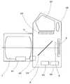
まず、本発明の実施例1のデジタルカメラ装置を図1及び図2を参照して説明する。
本発明の実施例1のデジタルカメラ装置は、交換レンズ1がマウント1aを介してデジタルカメラ部2に装着可能なデジタル一眼レフカメラから成るが、本発明はデジタル一眼レフカメラに限定されず、デジタルスチルカメラ、ビデオカメラ、テレビカメラ等の全てのデジタルカメラ装置に適用される。
交換レンズ1には、交換レンズ1の射出瞳から像面までの距離である瞳距離の情報が記憶されるレンズ情報記憶部61及びレンズ情報記憶部61の情報を必要に応じてデジタルカメラ部2に通信するレンズ情報通信部62が設けられる。
一方、デジタルカメラ部2の撮像光路上には、回転ミラー23、ピント板24、ペンタプリズム25、接眼レンズ26、光学ローパスフィルター3、撮像素子5が設けられる。光学ローパスフィルター3は撮像素子5の直前に設けられる。
さらに、デジタルカメラ部2には、光学ローパスフィルター3の欠陥位置情報を記憶している欠陥位置記憶手段63及び欠陥の補正演算を行なう欠陥補正演算部64が設けられる。
ファインダー観察時には交換レンズ1を透過した光像は回転ミラー23で反射され、ピント板24に結像し、ペンタプリズム25、接眼レンズ26を介して観察される。
撮影時には回転ミラー23は撮影光路から退避し、光学ローパスフィルター3を経て撮像素子5で撮像される。First, a digital camera device according to a first embodiment of the present invention will be described with reference to FIGS.
The digital camera device according to the first embodiment of the present invention includes a digital single-lens reflex camera in which the
In the
On the other hand, on the imaging optical path of the
Further, the
At the time of finder observation, the light image transmitted through the
At the time of photographing, the
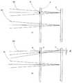
本実施例1では、レンズ情報として交換レンズ1の瞳距離情報を使用して出力の欠陥補正を行なう。
図2(a)に示されるように瞳距離が長い場合には光学ローパスフィルター3上の欠陥の位置と撮像素子5上の欠陥の出力位置はほぼ同じ場所であるが、図2(b)に示されるように瞳距離が短い場合には光学ローパスフィルター3上の欠陥の位置と撮像素子5上の欠陥の出力位置とはずれを生じる。
ここで、瞳距離をP、撮像素子5上の像高をhとすると、光学ローパスフィルター3上の欠陥の位置と撮像素子5上の欠陥の出力位置のずれΔは、光学ローパスフィルター3と撮像素子5間の距離をLとするとき、
Δ=L・h・P0
となる。
また、図2(a)(b)において、軸上光束91、軸外光束92、軸上光束93、軸外光束94、欠陥の中央を通る光線95及び欠陥の端を通る光束96が示される。
撮影時においては撮影画像の出力に対し、欠陥位置記憶手段63に記憶されている欠陥の位置情報にレンズ情報記憶部61からのレンズ瞳距離情報を基に位置補正を加え欠陥補正演算部64で補正し出力する。
このようにして瞳位置の異なる交換レンズやズーム位置で正確な欠陥の補正を行なうことができる。
このため、光学ローパスフィルター3の欠陥の補正に、欠陥の位置情報の他に、さらに、レンズの射出瞳から撮像面までの瞳距離であるレンズ情報も併せて使用し撮影画像の該当する画素の出力を補正するため、より正確な画像補正ができ、より良好な画像が得られる。In the first embodiment, output defect correction is performed using pupil distance information of the
As shown in FIG. 2A, when the pupil distance is long, the position of the defect on the optical low-pass filter 3 and the output position of the defect on the
Here, when the pupil distance is P and the image height on the
Δ = L · h · P0
It becomes.
2A and 2B, an on-
At the time of shooting, the defect
In this way, accurate defect correction can be performed at interchangeable lenses and zoom positions with different pupil positions.
For this reason, in addition to the defect position information, lens information that is the pupil distance from the exit pupil of the lens to the imaging surface is also used for correcting the defect of the optical low-pass filter 3, and the corresponding pixel of the photographed image is corrected. Since the output is corrected, more accurate image correction can be performed and a better image can be obtained.
次に、本発明の実施例2のデジタルカメラ装置を図1及び図3を参照して説明する。
本発明に関する第2の実施例のデジタルカメラ装置は、交換レンズ1がマウント1aを介してデジタルカメラ部2に装着可能なデジタル一眼レフカメラであるが、本発明はデジタル一眼レフカメラに限定されず、デジタルスチルカメラ、ビデオカメラ、テレビカメラ等の全てのデジタルカメラ装置に適用される。
交換レンズ1にはレンズの射出瞳から像面までの距離である瞳距離の情報が記憶されているレンズ情報記憶部61、レンズ情報記憶部61の情報を必要に応じてデジタルカメラ部2に通信するレンズ情報通信部62を有している。
一方、デジタルカメラ部2の撮像光路上には、回転ミラー23、ピント板24、ペンタプリズム25、接眼レンズ26、光学ローパスフィルター3、撮像素子5が設けられる。光学ローパスフィルター3は撮像素子5の直前に設けられる。
さらに、デジタルカメラ部2は、光学ローパスフィルター3の欠陥位置情報を記憶している欠陥位置記憶手段63、欠陥の補正演算を行なう欠陥補正演算部64を有している
ファインダー観察時においては、交換レンズ 1を透過した光像はファインダー観察時には回転ミラー23で反射してピント板 24に結像し、ペンタプリズム25、接眼レンズ 26を介して観察される。
撮影時において回転ミラー23は撮影光路から退避し、光学ローパスフィルター3を経て撮像素子5で撮像される。Next, a digital camera device according to a second embodiment of the present invention will be described with reference to FIGS.
The digital camera apparatus according to the second embodiment of the present invention is a digital single-lens reflex camera in which the
In the
On the other hand, on the imaging optical path of the
Further, the
At the time of photographing, the rotating
本実施例2では、レンズ情報としてレンズのFナンバー情報を使用して出力の欠陥補正を行なう。
図3(a)に示されるようにFナンバーが暗い小絞りの場合には光学ローパスフィルター3上の欠陥の位置と撮像素子5上の欠陥の画像信号出力55の出力位置はほぼ同じ範囲の広がりをもつが、図3(b)に示されるようにFナンバーが明るい状態の場合には撮像素子5上の欠陥の画像信号出力56の出力範囲は広がりを持つ。この関係はFナンバーに比例し発生する。
撮影時には撮影画像の出力に対し、欠陥位置記憶手段63に記憶されている欠陥の位置情報に、レンズ情報記憶部61からのFナンバー情報を基に広がりの補正を加え欠陥補正演算部64で補正し出力する。このようにしてFナンバーの異なる状態で正確な欠陥の補正を行なうことができる。
このため、光学ローパスフィルター3の欠陥の補正に、欠陥の位置情報の他に、さらに、レンズのFナンバーであるレンズ情報も併せて使用し撮影画像の該当する画素の出力を補正するため、より正確な画像補正ができ、より良好な画像が得られる。
上記実施例1及び2において用いられるレンズの射出瞳から撮像面までの瞳距離であるレンズ情報及びレンズのFナンバーのレンズ情報以外の光学パラメータ、例えば、各像高の開口効率、各像高の開口形状、ズーム位置毎のパラメータ情報等も補正に使用できるものがある。In Example 2, output defect correction is performed using lens F-number information as lens information.
As shown in FIG. 3A, in the case of a small stop with a dark F number, the position of the defect on the optical low-pass filter 3 and the output position of the
At the time of shooting, the defect
For this reason, in addition to the defect position information, the lens information which is the F number of the lens is also used for correcting the defect of the optical low-pass filter 3 to correct the output of the corresponding pixel of the photographed image. Accurate image correction can be performed, and a better image can be obtained.
Optical parameters other than the lens information that is the pupil distance from the exit pupil of the lens used in the first and second embodiments to the imaging surface and the lens information of the F-number of the lens, for example, the aperture efficiency of each image height, the image height Some aperture information, parameter information for each zoom position, and the like can also be used for correction.
1:交換レンズ、2:デジタルカメラ部、3:光学ローパスフィルター、5:撮像素子、8:光学ローパスフィルター上の欠陥、23:回転ミラー、24:ピント板、25:ペンタプリズム、26:接眼レンズ、55,56:画像信号出力、61:レンズ情報記憶部、62:レンズ情報通信部、63:欠陥位置記憶手段、64:欠陥補正演算部、91:軸上光束、92:軸外光束、
93:軸上光束、94:軸外光束、95:欠陥の中央を通る光線、
96:欠陥の端を通る光束1: Interchangeable lens, 2: Digital camera unit, 3: Optical low-pass filter, 5: Image sensor, 8: Defect on optical low-pass filter, 23: Rotating mirror, 24: Focus plate, 25: Penta prism, 26:
93: On-axis light beam, 94: Off-axis light beam, 95: Light beam passing through the center of the defect,
96: Light flux passing through the edge of the defect
Claims (4)
Translated fromJapanese前記欠陥の位置情報を基に撮影画像の該当する画素の出力を補正する補正手段と、を有することを特徴とするデジタルカメラ装置。Defect position storage means for storing position information of defects that are flaws and foreign matters existing on the imaging optical path;
A digital camera apparatus comprising: correction means for correcting an output of a corresponding pixel of the photographed image based on the position information of the defect.
前記欠陥の位置情報の他に前記レンズ情報を基に撮影画像の該当する画素の出力を補正する前記補正手段と、を有する請求項1に記載のデジタルカメラ装置。Lens information storage means for storing lens information;
The digital camera apparatus according to claim 1, further comprising: a correction unit that corrects an output of a corresponding pixel of a captured image based on the lens information in addition to the position information of the defect.
4. The digital camera device according to claim 3, wherein the lens information is a pupil distance from an exit pupil of the lens to an imaging surface, or an F number of the lens.
Priority Applications (1)
| Application Number | Priority Date | Filing Date | Title |
|---|---|---|---|
| JP2005044724AJP2006229898A (en) | 2005-02-21 | 2005-02-21 | Digital camera device |
Applications Claiming Priority (1)
| Application Number | Priority Date | Filing Date | Title |
|---|---|---|---|
| JP2005044724AJP2006229898A (en) | 2005-02-21 | 2005-02-21 | Digital camera device |
Publications (2)
| Publication Number | Publication Date |
|---|---|
| JP2006229898Atrue JP2006229898A (en) | 2006-08-31 |
| JP2006229898A5 JP2006229898A5 (en) | 2008-04-10 |
Family
ID=36990809
Family Applications (1)
| Application Number | Title | Priority Date | Filing Date |
|---|---|---|---|
| JP2005044724APendingJP2006229898A (en) | 2005-02-21 | 2005-02-21 | Digital camera device |
Country Status (1)
| Country | Link |
|---|---|
| JP (1) | JP2006229898A (en) |
Cited By (1)
| Publication number | Priority date | Publication date | Assignee | Title |
|---|---|---|---|---|
| JP2013093695A (en)* | 2011-10-25 | 2013-05-16 | Canon Inc | Imaging device, control method therefor, and program |
Citations (5)
| Publication number | Priority date | Publication date | Assignee | Title |
|---|---|---|---|---|
| JPH08328070A (en)* | 1995-03-31 | 1996-12-13 | Asahi Optical Co Ltd | TTL exposure control device for interchangeable lens type camera |
| JP2000196953A (en)* | 1998-12-25 | 2000-07-14 | Olympus Optical Co Ltd | Camera system |
| JP2002209147A (en)* | 2001-01-12 | 2002-07-26 | Fuji Photo Film Co Ltd | Digital camera and operation control method thereof |
| JP2004222233A (en)* | 2002-12-27 | 2004-08-05 | Nikon Corp | Image processing apparatus and image processing program |
| JP2004317377A (en)* | 2003-04-17 | 2004-11-11 | Nikon Corp | Foreign object detection jig for interchangeable lens digital camera, camera body and foreign object detection system |
- 2005
- 2005-02-21JPJP2005044724Apatent/JP2006229898A/enactivePending
Patent Citations (5)
| Publication number | Priority date | Publication date | Assignee | Title |
|---|---|---|---|---|
| JPH08328070A (en)* | 1995-03-31 | 1996-12-13 | Asahi Optical Co Ltd | TTL exposure control device for interchangeable lens type camera |
| JP2000196953A (en)* | 1998-12-25 | 2000-07-14 | Olympus Optical Co Ltd | Camera system |
| JP2002209147A (en)* | 2001-01-12 | 2002-07-26 | Fuji Photo Film Co Ltd | Digital camera and operation control method thereof |
| JP2004222233A (en)* | 2002-12-27 | 2004-08-05 | Nikon Corp | Image processing apparatus and image processing program |
| JP2004317377A (en)* | 2003-04-17 | 2004-11-11 | Nikon Corp | Foreign object detection jig for interchangeable lens digital camera, camera body and foreign object detection system |
Cited By (1)
| Publication number | Priority date | Publication date | Assignee | Title |
|---|---|---|---|---|
| JP2013093695A (en)* | 2011-10-25 | 2013-05-16 | Canon Inc | Imaging device, control method therefor, and program |
Similar Documents
| Publication | Publication Date | Title |
|---|---|---|
| USRE48552E1 (en) | Method and system for image construction using multiple exposures | |
| US8810713B2 (en) | Image pickup apparatus and image pickup device for performing auto-focusing | |
| JP4757185B2 (en) | Optical equipment | |
| US20090051792A1 (en) | Digital single-lens reflex camera | |
| JP2020528700A (en) | Methods and mobile terminals for image processing using dual cameras | |
| JP2020537382A (en) | Methods and equipment for dual camera-based imaging and storage media | |
| JPH09181913A (en) | Camera system | |
| US9172887B2 (en) | Imaging apparatus, control method of imaging apparatus, interchangeable lens and lens-interchangeable type imaging apparatus body | |
| JP2005128092A (en) | Camera | |
| JP2015194686A (en) | Imaging apparatus | |
| JP6656584B2 (en) | Imaging equipment | |
| JP5964772B2 (en) | Lens information registration system, lens information server and camera body used for lens information registration system | |
| JP2005258202A (en) | Camera system, camera body, photographing lens barrel and flash light emitting device | |
| JP2006229898A (en) | Digital camera device | |
| KR20060063724A (en) | Imaging Apparatus, Imaging Method, and Program for Imaging Processing | |
| JP2006197406A (en) | Image pickup device | |
| JP4938922B2 (en) | Camera system | |
| JP2010134480A (en) | Camera | |
| JP2008245236A (en) | Imaging apparatus and defective pixel correcting method | |
| JP2002290811A (en) | Imaging device, method and program for image processing, and information recording medium | |
| JP7592391B2 (en) | Imaging device | |
| JP2008147751A (en) | Imaging device | |
| JP2015201812A (en) | Image processing method, program, and imaging apparatus | |
| JP6559354B2 (en) | Imaging device | |
| JP2018207412A (en) | Method for controlling imaging apparatus |
Legal Events
| Date | Code | Title | Description |
|---|---|---|---|
| A521 | Request for written amendment filed | Free format text:JAPANESE INTERMEDIATE CODE: A523 Effective date:20080218 | |
| A621 | Written request for application examination | Free format text:JAPANESE INTERMEDIATE CODE: A621 Effective date:20080218 | |
| RD01 | Notification of change of attorney | Free format text:JAPANESE INTERMEDIATE CODE: A7421 Effective date:20090406 | |
| RD04 | Notification of resignation of power of attorney | Free format text:JAPANESE INTERMEDIATE CODE: A7424 Effective date:20100201 | |
| A977 | Report on retrieval | Free format text:JAPANESE INTERMEDIATE CODE: A971007 Effective date:20100310 | |
| A131 | Notification of reasons for refusal | Free format text:JAPANESE INTERMEDIATE CODE: A131 Effective date:20100323 | |
| A521 | Request for written amendment filed | Free format text:JAPANESE INTERMEDIATE CODE: A523 Effective date:20100524 | |
| RD01 | Notification of change of attorney | Free format text:JAPANESE INTERMEDIATE CODE: A7421 Effective date:20100630 | |
| A02 | Decision of refusal | Free format text:JAPANESE INTERMEDIATE CODE: A02 Effective date:20110315 |