JP2006228407A - Method of preventing fixed pattern programming - Google Patents
Method of preventing fixed pattern programmingDownload PDFInfo
- Publication number
- JP2006228407A JP2006228407AJP2006010819AJP2006010819AJP2006228407AJP 2006228407 AJP2006228407 AJP 2006228407AJP 2006010819 AJP2006010819 AJP 2006010819AJP 2006010819 AJP2006010819 AJP 2006010819AJP 2006228407 AJP2006228407 AJP 2006228407A
- Authority
- JP
- Japan
- Prior art keywords
- data
- scrambling
- periodically
- programming
- pattern
- Prior art date
- Legal status (The legal status is an assumption and is not a legal conclusion. Google has not performed a legal analysis and makes no representation as to the accuracy of the status listed.)
- Pending
Links
Images


Classifications
- G—PHYSICS
- G11—INFORMATION STORAGE
- G11C—STATIC STORES
- G11C16/00—Erasable programmable read-only memories
- G11C16/02—Erasable programmable read-only memories electrically programmable
- G11C16/06—Auxiliary circuits, e.g. for writing into memory
- G11C16/10—Programming or data input circuits
- G—PHYSICS
- G06—COMPUTING OR CALCULATING; COUNTING
- G06F—ELECTRIC DIGITAL DATA PROCESSING
- G06F12/00—Accessing, addressing or allocating within memory systems or architectures
- G06F12/14—Protection against unauthorised use of memory or access to memory
- G06F12/1408—Protection against unauthorised use of memory or access to memory by using cryptography
- G—PHYSICS
- G11—INFORMATION STORAGE
- G11C—STATIC STORES
- G11C11/00—Digital stores characterised by the use of particular electric or magnetic storage elements; Storage elements therefor
- G11C11/56—Digital stores characterised by the use of particular electric or magnetic storage elements; Storage elements therefor using storage elements with more than two stable states represented by steps, e.g. of voltage, current, phase, frequency
- G11C11/5621—Digital stores characterised by the use of particular electric or magnetic storage elements; Storage elements therefor using storage elements with more than two stable states represented by steps, e.g. of voltage, current, phase, frequency using charge storage in a floating gate
- G11C11/5628—Programming or writing circuits; Data input circuits
- G11C11/5635—Erasing circuits
- G—PHYSICS
- G11—INFORMATION STORAGE
- G11C—STATIC STORES
- G11C16/00—Erasable programmable read-only memories
- G11C16/02—Erasable programmable read-only memories electrically programmable
- G11C16/06—Auxiliary circuits, e.g. for writing into memory
- G11C16/10—Programming or data input circuits
- G11C16/14—Circuits for erasing electrically, e.g. erase voltage switching circuits
- G11C16/16—Circuits for erasing electrically, e.g. erase voltage switching circuits for erasing blocks, e.g. arrays, words, groups
- G—PHYSICS
- G11—INFORMATION STORAGE
- G11C—STATIC STORES
- G11C16/00—Erasable programmable read-only memories
- G11C16/02—Erasable programmable read-only memories electrically programmable
- G11C16/06—Auxiliary circuits, e.g. for writing into memory
- G11C16/26—Sensing or reading circuits; Data output circuits
- G—PHYSICS
- G11—INFORMATION STORAGE
- G11C—STATIC STORES
- G11C16/00—Erasable programmable read-only memories
- G11C16/02—Erasable programmable read-only memories electrically programmable
- G11C16/06—Auxiliary circuits, e.g. for writing into memory
- G11C16/34—Determination of programming status, e.g. threshold voltage, overprogramming or underprogramming, retention
- G11C16/3404—Convergence or correction of memory cell threshold voltages; Repair or recovery of overerased or overprogrammed cells
- G—PHYSICS
- G11—INFORMATION STORAGE
- G11C—STATIC STORES
- G11C16/00—Erasable programmable read-only memories
- G11C16/02—Erasable programmable read-only memories electrically programmable
- G11C16/06—Auxiliary circuits, e.g. for writing into memory
- G11C16/34—Determination of programming status, e.g. threshold voltage, overprogramming or underprogramming, retention
- G11C16/3436—Arrangements for verifying correct programming or erasure
- G11C16/344—Arrangements for verifying correct erasure or for detecting overerased cells
- G11C16/3445—Circuits or methods to verify correct erasure of nonvolatile memory cells
- G—PHYSICS
- G11—INFORMATION STORAGE
- G11C—STATIC STORES
- G11C16/00—Erasable programmable read-only memories
- G11C16/02—Erasable programmable read-only memories electrically programmable
- G11C16/06—Auxiliary circuits, e.g. for writing into memory
- G11C16/34—Determination of programming status, e.g. threshold voltage, overprogramming or underprogramming, retention
- G11C16/349—Arrangements for evaluating degradation, retention or wearout, e.g. by counting erase cycles
- G—PHYSICS
- G11—INFORMATION STORAGE
- G11C—STATIC STORES
- G11C16/00—Erasable programmable read-only memories
- G11C16/02—Erasable programmable read-only memories electrically programmable
- G11C16/04—Erasable programmable read-only memories electrically programmable using variable threshold transistors, e.g. FAMOS
- G11C16/0466—Erasable programmable read-only memories electrically programmable using variable threshold transistors, e.g. FAMOS comprising cells with charge storage in an insulating layer, e.g. metal-nitride-oxide-silicon [MNOS], silicon-oxide-nitride-oxide-silicon [SONOS]
- G11C16/0475—Erasable programmable read-only memories electrically programmable using variable threshold transistors, e.g. FAMOS comprising cells with charge storage in an insulating layer, e.g. metal-nitride-oxide-silicon [MNOS], silicon-oxide-nitride-oxide-silicon [SONOS] comprising two or more independent storage sites which store independent data
- G—PHYSICS
- G11—INFORMATION STORAGE
- G11C—STATIC STORES
- G11C2216/00—Indexing scheme relating to G11C16/00 and subgroups, for features not directly covered by these groups
- G11C2216/12—Reading and writing aspects of erasable programmable read-only memories
- G11C2216/18—Flash erasure of all the cells in an array, sector or block simultaneously
Landscapes
- Engineering & Computer Science (AREA)
- Computer Security & Cryptography (AREA)
- Theoretical Computer Science (AREA)
- Computer Hardware Design (AREA)
- Physics & Mathematics (AREA)
- General Engineering & Computer Science (AREA)
- General Physics & Mathematics (AREA)
- Read Only Memory (AREA)
- Non-Volatile Memory (AREA)
- Semiconductor Memories (AREA)
Abstract
Description
Translated fromJapanese本発明は、概括的には、プログラミングや消去のような、不揮発性メモリ(NVM)アレイのメモリセルを作動させることに、具体的には、データスクランブルによるような、セルのプログラム及び消去履歴における大きな違いを防止するための方法に関する。 The present invention generally relates to operating memory cells of a non-volatile memory (NVM) array, such as programming and erasing, specifically in cell programming and erasing history, such as by data scrambling. It relates to methods for preventing major differences.
本出願は、2005年1月19日出願の米国仮出願第60/644,569号の優先権を請求し、同出願を参考文献としてここに援用する。 This application claims priority from US Provisional Application No. 60 / 644,569, filed Jan. 19, 2005, which is hereby incorporated by reference.
最近、不揮発性メモリ製品には、メモリセルを電気的にプログラムし、消去する能力が組み込まれている。殆どの場合、消去動作は、セル毎に個別にではなくセルのサブセットで実行され、プログラミング動作の間に普通に実行される。これは、セルが所定のレベルをパスしているという確認(消去確認)を含め、最終(最も遅い)セルが消去を終了するまで、消去条件がサブセットに適用されることを意味している。 Recently, non-volatile memory products have built in the ability to electrically program and erase memory cells. In most cases, the erase operation is performed on a subset of cells rather than individually for each cell, and is typically performed during a programming operation. This means that the erasure condition is applied to the subset until the last (latest) cell finishes erasing, including confirmation that the cell passes a predetermined level (erase confirmation).
NROM(窒化物読み取り専用メモリ)技術でのように、消去の間にトンネリング強化ホットホールインジェクションを組み込んだメモリ製品は、図1で分かるように、注入ホールを作るため、バンド間トンネリングを通して、トランジスタ接合に高いバイアスを掛ける必要がある。電荷注入は、正しいデバイス動作を保証するように制御されねばならないので、通常は、ステップ毎に確認するアルゴリズムが実施される。代表的なアルゴリズムでは、電荷が一定のバイアスを掛けて注入され、その後、セルがその目的地に達しているか否かを確認するため、確認動作が続く。目的地に到達していなければ、更に強い電荷注入がより高いバイアスを掛けて始動され、逆の場合も同じである。 As in NROM (nitride read-only memory) technology, memory products that incorporate tunneling enhanced hot hole injection during erasure, as can be seen in FIG. 1, through interband tunneling to create a transistor junction. Need to be highly biased. Since charge injection must be controlled to ensure correct device operation, a step-by-step algorithm is usually implemented. In a typical algorithm, charge is injected with a constant bias, and then a check operation continues to check whether the cell has reached its destination. If the destination has not been reached, a stronger charge injection is started with a higher bias, and vice versa.
図2は、NROMデバイスに関する先行技術による消去アルゴリズムの代表的な流れ図である。 FIG. 2 is a representative flow diagram of a prior art erase algorithm for an NROM device.
消去パルスが、セルのビットを消去するために選択されるが、負のゲート電圧(Vg又はVcvpn−電荷ポンプからの電圧)と正のドレイン電圧(Vppd)を選択(ダイヤルイン)する段階(ステップ201)を備えている。次に、消去パルスが、セル集団内のビットに加えられる(ステップ202)。セルの閾値電圧Vtは、メモリセルの閾値電圧が消去確認(EV)電圧レベルまで下がっているか否か検査する消去確認ステップで読み取られる(ステップ203)。 An erase pulse is selected to erase the bit of the cell, but selects (dial-in) a negative gate voltage (Vg or Vcvpn—the voltage from the charge pump) and a positive drain voltage (Vppd) (steps). 201). Next, an erase pulse is applied to the bits in the cell population (step 202). The threshold voltage Vt of the cell is read in an erase confirmation step that checks whether the threshold voltage of the memory cell has dropped to the erase confirmation (EV) voltage level (step 203).
どのセルもEVをパスしていなければ、新しいVppdレベルが、強い(即ち大きい)増分で設定(ダイヤルイン)される(ステップ204)。幾つかのセルがEVをパスしていれば、新しいVppdレベルは、弱い(即ち、比較的小さい)増分で設定される(ステップ205)。このプロセスは、消去パルスが全てのセルに加えられるまで続く。各サブグループは、信頼性を改良するため、完全消去を達成するために用いられた最後のパルスよりも高いレベルの余分な消去パルスを受け取る。追加パルスの印加は、本出願の譲受人に譲渡されている米国特許第6,700,818号、米国特許出願第20050117395号、第20050058005号のような様々な特許文書に教示されており、その開示を参考文献としてここに援用する。 If no cell passes the EV, a new Vppd level is set (dial-in) in strong (ie, large) increments (step 204). If several cells pass the EV, the new Vppd level is set in weak (ie, relatively small) increments (step 205). This process continues until an erase pulse is applied to all cells. Each subgroup receives an extra erase pulse at a higher level than the last pulse used to achieve full erase to improve reliability. The application of additional pulses is taught in various patent documents such as U.S. Patent Nos. 6,700,818, U.S. Patent Application Nos. 20050117395 and 2005080005, assigned to the assignee of the present application. The disclosure is incorporated herein by reference.
トンネリング強化ホットホールインジェクションでは、図2に示すこのプロセスが、通常、メモリセルの両側で別々に実行されねばならず、結果的に長い消去時間と低い性能に帰結する。 In tunneling enhanced hot hole injection, this process shown in FIG. 2 typically must be performed separately on both sides of the memory cell, resulting in long erase times and poor performance.
セルのサブセットに記憶されているデータは、本質的に無作為なことが多く、消去動作の前、或るセルはプログラムされた状態にあり、又別のセルは消去された状態にある。従って、特別な行動を取らなければ、以前にプログラムされ消去動作が実施されたセルは、消去確認レベルに近いか又はそのレベルにある閾値レベルに達し、一方、プログラムされていなかったセルは過剰消去され、閾値電圧が消去確認レベルを相当下回ることもあり得る。これを図3に示しており、この図は、先行技術による、セルのサブセットの閾値電圧分布の、あらゆる動作が実行される前の自然な状態と、消去された後を、或るサブグループだけが以前にプログラムされていた場合について示している。消去されたセルの分布にはピークが2つある。高い方のピークは、以前にプログラムされたセルの閾値電圧分布であり、低い方のピークは、プログラムされていないセル、即ち過剰消去されたセルの閾値電圧分布である。 Data stored in a subset of cells is often random in nature, with one cell in a programmed state and another cell in an erased state prior to an erase operation. Thus, if no special action is taken, a cell that has been programmed and erased previously has reached a threshold level that is near or at the erase verify level, while a cell that has not been programmed is over-erased. It is possible that the threshold voltage is considerably below the erase confirmation level. This is illustrated in FIG. 3, which shows the natural state of the threshold voltage distribution of a subset of cells according to the prior art before any operation is performed and only after a certain subgroup. Shows the case where was previously programmed. There are two peaks in the distribution of erased cells. The higher peak is the threshold voltage distribution of previously programmed cells, and the lower peak is the threshold voltage distribution of unprogrammed cells, ie, over-erased cells.
過剰消去の場合、幾つかの懸念が生じる。過剰消去されたセルは、漏洩し易くなり、即ち、「オン」状態(n−MOSFETベースのメモリセルの正のゲート電圧)にバイアスされなくとも電流を流すことになりかねない。過剰消去されたセルは、プログラムし難くなり、即ち、セルをプログラムされた状態(所定のレベル、プログラム確認レベル以上)にするのに過剰な電圧と時間が必要となる。過剰消去されたセルと、そうでないセルとの間で、動作条件(プログラム及び消去)に実質的な差が出てくる。これらの影響が積み重なると、メモリデバイスが故障し、即ちデータの完全性が失われる。 In the case of over-erasing, several concerns arise. Over-erased cells are prone to leakage, i.e., current can flow without being biased to the "on" state (the positive gate voltage of n-MOSFET based memory cells). Over-erased cells are difficult to program, that is, excessive voltage and time are required to bring the cells into a programmed state (predetermined level, program verify level and above). There is a substantial difference in operating conditions (program and erase) between cells that are over-erased and cells that are not. When these effects accumulate, the memory device fails, i.e., the integrity of the data is lost.
図4は、先行技術による、固定パターンの多数回のサイクリング(105サイクル)とそれに続くチェッカー盤パターンのプログラミングの後の、メモリアレイ内のセルのサブグループにおける閾値電圧分布を示している。十分な過剰消去防止法が無いため、プログラミングテイルの形成されているのが示されている。4, according to the prior art, after the programming of multiple cycling(105 cycles) and checkerboard pattern subsequent fixed pattern shows the threshold voltage distribution in the sub-group of cells in the memory array. It is shown that a programming tail is formed because there is not enough over-erasure protection.
セルの過剰消去を防止する先行技術の方法は、消去サブグループを分割する段階を含んでおり、消去サブグループが小さいほど消去の均一性が良くなることが保証されるという利点がある。しかしながら、オーバーヘッドが加わり、設計が複雑になるという不利な点がある。別の先行技術の方法は、消去前にプログラムする段階を含んでおり、セルは、プログラムされなければ、安定して消去されないようになっている。しかしながら、こうするのは、時間及び電力の点で相当な性能上の負担を抱え込むことになる。 Prior art methods for preventing over-erasing of cells include the step of dividing the erase subgroup, with the advantage that the smaller the erase subgroup, the better the erase uniformity. However, there is a disadvantage that the overhead is added and the design is complicated. Another prior art method includes a step of programming prior to erasure, so that the cell is not stably erased if not programmed. However, doing this places a considerable performance burden in terms of time and power.
別の先行技術方法は、消去後にプログラムする段階を含んでおり、セルが設定レベルを超えて過剰消去されないことを保証している。しかしながら、この方法も、時間及び電力の点で相当な性能上の負担を抱え込むことになる。
本発明は、以下に説明するように、固定パターンのプログラミングを防止し、メモリアレイのセルのプログラム及び消去の履歴における大きな違いを防止するための方法を提供するよう努めている。本発明について、NVMアレイのメモリセル、特に単一ビット、二重ビット、多重ビット及びマルチレベルのNROMセルに関連付けて以下に詳細に説明する。しかしながら、本発明は、NROMアレイに限定されるものではないことを強調しておく。 The present invention strives to provide a method for preventing fixed pattern programming and preventing major differences in memory array cell programming and erasing history, as described below. The present invention is described in detail below in connection with NVM array memory cells, particularly single bit, double bit, multi-bit and multi-level NROM cells. However, it is emphasized that the present invention is not limited to NROM arrays.
本発明の或る実施形態によれば、固定パターンのプログラミングを防止するための方法が提供されており、本方法は、データを、メモリアレイ内のメモリセルの或るパターンにプログラムする段階と、データが、メモリアレイ内の異なるパターンのメモリセルに記憶されるように、データを定期的にスクランブルすることによって固定パターンのプログラミングを防止する段階と、を含んでいる。 According to an embodiment of the present invention, a method for preventing programming of a fixed pattern is provided, the method comprising: programming data into a pattern of memory cells in a memory array; Preventing fixed pattern programming by periodically scrambling the data such that the data is stored in different patterns of memory cells in the memory array.
データは、データを定期的に反転させることによってスクランブルされる。加えて又は代わりに、データは、データの物理的アドレスを定期的に再配置することによってスクランブルされる。加えて又は代わりに、データは、プログラミング中にデータを混合パターンで巻き、読み取り動作の間に巻かれたデータを解くことによってスクランブルされる。加えて又は代わりに、データは、プログラム及び消去サイクルカウンターに従ってデータを定期的にスクランブルすることによってスクランブルされる。データは、無作為的に又は準無作為的に定期的にスクランブルしてもよい。 Data is scrambled by periodically inverting the data. In addition or alternatively, the data is scrambled by periodically relocating the physical address of the data. In addition or alternatively, the data is scrambled by wrapping the data in a mixed pattern during programming and unwinding the data wrapped during the read operation. In addition or alternatively, the data is scrambled by periodically scrambling the data according to a program and erase cycle counter. The data may be scrambled periodically randomly or semi-randomly.
限定するわけではないが、本発明の或る実施形態によれば、データは、メモリアレイ内に記憶されているパラメーターの関数としてスクランブルされる。記憶されているパラメーターは、データと関連付けてプログラムされる。 Without limitation, according to some embodiments of the present invention, data is scrambled as a function of parameters stored in the memory array. The stored parameters are programmed in association with the data.
加えて又は代わりに、データは、データの論理的及び/又は物理的アドレスの関数としてスクランブルされる。 In addition or alternatively, the data is scrambled as a function of the logical and / or physical address of the data.
本発明は、以下の詳細な説明を添付図面と関連付けて読めば、十分に理解し把握頂けるであろう。 The present invention will be more fully understood and understood when the following detailed description is read in conjunction with the accompanying drawings.
図5は、本発明の或る実施形態による、不揮発性メモリセルアレイ内の固定パターンプログラミングを防止するための方法を示している。具体的には、図5は、以下に説明するように、データスクランブル実施におけるプログラミングの流れを示す単純化した流れ図である。 FIG. 5 illustrates a method for preventing fixed pattern programming in a non-volatile memory cell array according to an embodiment of the present invention. Specifically, FIG. 5 is a simplified flow diagram illustrating the programming flow in a data scramble implementation, as described below.
本発明の或る実施形態によれば、データを、メモリアレイ内の或るパターンのメモリセルにプログラムした後は、データが、メモリアレイ内の異なるパターンのメモリセルに記憶されるように、データを定期的にスクランブルする(ステップ500)ことによって、固定パターンのプログラミングが防止される。限定するわけではないが、本発明の或る実施形態では、実際の物理的にプログラムされたデータは、サイクル毎に強制的に変えられる(ステップ501)。従って、固定パターンプログラミングによって体系的な差が広がる率は、実質的に低減する。セルアレイにプログラムされた実際のデータは、ユーザーが入力データを操作した結果である(ステップ502)。この操作は、サイクル毎に変わる(ステップ503)か、カウンター又は所定の閾値パラメーターに依って定期的に変わる(ステップ504)。そのような操作は、限定するわけではないが、入力データを反転させる段階、それを桁送りする段階、それを移動させる段階、入力データ又は消去サブグループのビット、ワード、ページ又は何らかの他のデータサブセットの内部アドレスを混ぜ合わせる段階、又は、入力データを変化する混合パターンで巻く段階を含んでいる。混合パターンは、サイクル毎に、又は、固定している、変化している又は無作為の他の何らかの期間で変わる(ステップ505)。 According to certain embodiments of the present invention, after programming data into a pattern of memory cells in the memory array, the data is stored in a different pattern of memory cells in the memory array. Is periodically scrambled (step 500) to prevent fixed pattern programming. Without limitation, in one embodiment of the present invention, the actual physically programmed data is forced to change from cycle to cycle (step 501). Therefore, the rate at which systematic differences are spread by fixed pattern programming is substantially reduced. The actual data programmed in the cell array is the result of the user operating the input data (step 502). This operation changes from cycle to cycle (step 503) or periodically depending on a counter or a predetermined threshold parameter (step 504). Such operations include, but are not limited to, inverting the input data, shifting it, moving it, bits of input data or erase subgroups, words, pages or some other data It includes the steps of mixing the internal addresses of the subsets or winding the input data with a mixed pattern that changes. The mixing pattern changes from cycle to cycle or at some other time period that is fixed, changing, or random (step 505).
限定するわけではないが、本発明の或る実施形態によれば、消去区画がページのグループ(それぞれ個々にプログラムされている)で構成されており、入力ページデータは、カウンター、及び消去区画の内側のページの位置によって決まる無作為又は準無作為パターンで巻かれている(ステップ506)。カウンターはサイクル毎に変わるので、ページの物理的アドレスにプログラムされている実際のデータも変わる(ステップ507)。更に、無作為又は準無作為パターンも、消去区画内のページの位置で決まるので、入力データが全ページで同じであっても、プログラムされている実際のデータは、ページ毎に変わる(ステップ508)。データ及びエラー検出パラメーターをスクランブルするのに用いられるカウンターは、同じ流れで物理的にプログラムされている(ステップ509)。エラー検出パラメーターについては、例えば、米国特許出願第10/695,457号(発行番号US20040136236)、及び対応するPCT出願WO2005/041108「不揮発性メモリアレイにおける読取エラー検出に関する方法、回路及びシステム」で論じられており、前者の開示をここに参考文献として援用するが、両方共に本発明の譲受人に譲渡されている。読み取りエラー率は、例えば、パリティビット、チェックサム、CRC及び様々な他の技法など、多様なエラー率のサンプリング及び/又はエラー検出技法を使って求められる。現在知られているか、将来考案される、あらゆるエラー検出コーティング及び/又は評価技法は、本発明に適用することができる。 Without limitation, according to some embodiments of the present invention, the erase section is comprised of a group of pages (each individually programmed), and the input page data includes a counter and an erase section. It is wound with a random or semi-random pattern determined by the position of the inner page (step 506). Since the counter changes from cycle to cycle, the actual data programmed into the physical address of the page also changes (step 507). Further, since the random or quasi-random pattern is also determined by the position of the page in the erasure section, even if the input data is the same for all pages, the actual data programmed varies from page to page (step 508). ). The counter used to scramble the data and error detection parameters is physically programmed with the same flow (step 509). Error detection parameters are discussed, for example, in US patent application Ser. No. 10 / 695,457 (issue number US20040136236) and corresponding PCT application WO2005 / 041108 “Methods, Circuits and Systems for Read Error Detection in Nonvolatile Memory Arrays”. The former disclosure is incorporated herein by reference, both of which are assigned to the assignee of the present invention. The read error rate is determined using various error rate sampling and / or error detection techniques, such as, for example, parity bits, checksum, CRC, and various other techniques. Any error detection coating and / or evaluation technique now known or devised in the future can be applied to the present invention.
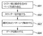
図6は、本発明の或る実施形態による、図5のデータスクランブル実施の読み取り動作を示している。データの信頼性は、スクランブル方式による影響を受けない。 FIG. 6 illustrates a read operation of the data scramble implementation of FIG. 5 according to an embodiment of the present invention. Data reliability is not affected by the scrambling scheme.
限定するわけではないが、本発明の或る実施形態では、エラー検出パラメーターを含めて、ページが読み取られる(ステップ601)。カウンターが用いられていれば、アルゴリズムがカウンターを評価する(ステップ602)。次に、使用された具体的なパターンが解析され(ステップ603)、データが抽出される(ステップ604)。 In one embodiment of the present invention, but not limited to, a page is read (step 601), including error detection parameters. If a counter is used, the algorithm evaluates the counter (step 602). Next, the specific pattern used is analyzed (step 603) and data is extracted (step 604).
以上、本発明を、特定の実施形態と関連付けて説明してきたが、当業者には、多くの代替、修正及び変更が自明であろう。従って、本発明は、そのような代替、修正及び変更の全てを包含するよう意図している。 Although the present invention has been described in connection with specific embodiments, many alternatives, modifications and variations will be apparent to those skilled in the art. Accordingly, the present invention is intended to embrace all such alternatives, modifications and variations.
Claims (11)
Translated fromJapaneseデータを、メモリアレイ内の或るパターンのメモリセルにプログラムする段階と、
前記データが、前記メモリアレイ内の異なるパターンのメモリセルに記憶されるように、前記データを定期的にスクランブルすることによって、固定パターンのプログラミングを防止する段階と、から成る方法。In a method for preventing programming of fixed patterns,
Programming data into a pattern of memory cells in a memory array;
Preventing the programming of a fixed pattern by periodically scrambling the data such that the data is stored in different patterns of memory cells in the memory array.
Applications Claiming Priority (1)
| Application Number | Priority Date | Filing Date | Title |
|---|---|---|---|
| US64456905P | 2005-01-19 | 2005-01-19 |
Publications (1)
| Publication Number | Publication Date |
|---|---|
| JP2006228407Atrue JP2006228407A (en) | 2006-08-31 |
Family
ID=36143177
Family Applications (3)
| Application Number | Title | Priority Date | Filing Date |
|---|---|---|---|
| JP2006010819APendingJP2006228407A (en) | 2005-01-19 | 2006-01-19 | Method of preventing fixed pattern programming |
| JP2006010811APendingJP2006228406A (en) | 2005-01-19 | 2006-01-19 | Erasing method, circuit, and system for one or more nonvolatile memory cells |
| JP2006010810APendingJP2006228405A (en) | 2005-01-19 | 2006-01-19 | Verification on partial erasure |
Family Applications After (2)
| Application Number | Title | Priority Date | Filing Date |
|---|---|---|---|
| JP2006010811APendingJP2006228406A (en) | 2005-01-19 | 2006-01-19 | Erasing method, circuit, and system for one or more nonvolatile memory cells |
| JP2006010810APendingJP2006228405A (en) | 2005-01-19 | 2006-01-19 | Verification on partial erasure |
Country Status (4)
| Country | Link |
|---|---|
| US (3) | US7468926B2 (en) |
| EP (3) | EP1686592A3 (en) |
| JP (3) | JP2006228407A (en) |
| CN (3) | CN1838328A (en) |
Cited By (11)
| Publication number | Priority date | Publication date | Assignee | Title |
|---|---|---|---|---|
| JP2008198299A (en)* | 2007-02-14 | 2008-08-28 | Toshiba Corp | Data writing method |
| JP2008217857A (en)* | 2007-02-28 | 2008-09-18 | Toshiba Corp | Memory controller and semiconductor device |
| JP2009104598A (en)* | 2007-09-28 | 2009-05-14 | Intel Corp | Suppressing power supply noise using data scrambling in ddr double data rate memory system |
| JP2009110476A (en)* | 2007-11-01 | 2009-05-21 | Konami Digital Entertainment Co Ltd | Storage processing device, information providing server, operation method, and program |
| JP2009157841A (en)* | 2007-12-27 | 2009-07-16 | Toshiba Corp | Memory system |
| JP2010503142A (en)* | 2006-09-08 | 2010-01-28 | サンディスク コーポレイション | Pseudo-random and command-driven bit compensation and its method for cycle effects in flash memory |
| KR20100121472A (en)* | 2007-12-31 | 2010-11-17 | 쌘디스크 코포레이션 | System, method and memory device providing data scrambling compatible with on-chip copy operation |
| JP2010538408A (en)* | 2007-09-07 | 2010-12-09 | サンディスク コーポレイション | Non-volatile memory and method for intra-page and inter-page on-chip data pseudo-randomization |
| US8843693B2 (en) | 2011-05-17 | 2014-09-23 | SanDisk Technologies, Inc. | Non-volatile memory and method with improved data scrambling |
| KR101517185B1 (en) | 2008-04-15 | 2015-05-04 | 삼성전자주식회사 | Memory system and operating method thereof |
| US9292428B2 (en) | 2012-09-05 | 2016-03-22 | Kabushiki Kaisha Toshiba | Memory system |
Families Citing this family (57)
| Publication number | Priority date | Publication date | Assignee | Title |
|---|---|---|---|---|
| US20070103980A1 (en)* | 2005-11-10 | 2007-05-10 | Gert Koebernick | Method for operating a semiconductor memory device and semiconductor memory device |
| US7734861B2 (en)* | 2006-09-08 | 2010-06-08 | Sandisk Corporation | Pseudo random and command driven bit compensation for the cycling effects in flash memory |
| US7606966B2 (en) | 2006-09-08 | 2009-10-20 | Sandisk Corporation | Methods in a pseudo random and command driven bit compensation for the cycling effects in flash memory |
| US7619934B2 (en)* | 2006-12-20 | 2009-11-17 | Spansion Llc | Method and apparatus for adaptive memory cell overerase compensation |
| US8370561B2 (en)* | 2006-12-24 | 2013-02-05 | Sandisk Il Ltd. | Randomizing for suppressing errors in a flash memory |
| KR101449673B1 (en) | 2006-12-24 | 2014-10-13 | 샌디스크 아이엘 엘티디 | Flash memory device, system and method with randomizing for suppressing error |
| US8127200B2 (en) | 2006-12-24 | 2012-02-28 | Sandisk Il Ltd. | Flash memory device and system with randomizing for suppressing errors |
| US8320191B2 (en) | 2007-08-30 | 2012-11-27 | Infineon Technologies Ag | Memory cell arrangement, method for controlling a memory cell, memory array and electronic device |
| US20090150595A1 (en)* | 2007-10-24 | 2009-06-11 | Avi Lavan | Balanced programming rate for memory cells |
| US7843728B2 (en)* | 2007-11-20 | 2010-11-30 | Kabushiki Kaisha Toshiba | Nonvolatile semiconductor storage device |
| US7995392B2 (en) | 2007-12-13 | 2011-08-09 | Kabushiki Kaisha Toshiba | Semiconductor memory device capable of shortening erase time |
| JP2009163782A (en)* | 2007-12-13 | 2009-07-23 | Toshiba Corp | Semiconductor memory device |
| US7813169B2 (en)* | 2008-01-18 | 2010-10-12 | Qimonda Flash Gmbh | Integrated circuit and method to operate an integrated circuit |
| KR101378365B1 (en) | 2008-03-12 | 2014-03-28 | 삼성전자주식회사 | Apparatus and method for hybrid detecting memory data |
| US8154918B2 (en)* | 2008-06-30 | 2012-04-10 | Sandisk Il Ltd. | Method for page- and block based scrambling in non-volatile memory |
| US8230158B2 (en)* | 2008-08-12 | 2012-07-24 | Micron Technology, Inc. | Memory devices and methods of storing data on a memory device |
| US8130552B2 (en)* | 2008-09-11 | 2012-03-06 | Sandisk Technologies Inc. | Multi-pass programming for memory with reduced data storage requirement |
| US8145855B2 (en) | 2008-09-12 | 2012-03-27 | Sandisk Technologies Inc. | Built in on-chip data scrambler for non-volatile memory |
| WO2010030701A1 (en)* | 2008-09-12 | 2010-03-18 | Sandisk Corporation | Built in on-chip data scrambler for non-volatile memory |
| US8429330B2 (en) | 2008-09-12 | 2013-04-23 | Sandisk Technologies Inc. | Method for scrambling data in which scrambling data and scrambled data are stored in corresponding non-volatile memory locations |
| JP5492679B2 (en)* | 2009-06-30 | 2014-05-14 | パナソニック株式会社 | Storage device and memory controller |
| US8874825B2 (en) | 2009-06-30 | 2014-10-28 | Sandisk Technologies Inc. | Storage device and method using parameters based on physical memory block location |
| US8036044B2 (en)* | 2009-07-16 | 2011-10-11 | Sandisk Technologies Inc. | Dynamically adjustable erase and program levels for non-volatile memory |
| KR20110055178A (en)* | 2009-11-19 | 2011-05-25 | 삼성전자주식회사 | Flash memory device and memory system including it |
| US8130551B2 (en) | 2010-03-31 | 2012-03-06 | Sandisk Technologies Inc. | Extra dummy erase pulses after shallow erase-verify to avoid sensing deep erased threshold voltage |
| KR20120002760A (en)* | 2010-07-01 | 2012-01-09 | 삼성전자주식회사 | Data recording method and data recording apparatus for improving the operational reliability of the NAND flash memory |
| KR101710089B1 (en) | 2010-08-26 | 2017-02-24 | 삼성전자주식회사 | Nonvolatile memory device, operating method thereof and memory system including the same |
| US8953318B1 (en)* | 2010-09-13 | 2015-02-10 | The Board Of Trustees Of The University Of Alabama, For And On Behalf Of The University Of Alabama In Huntsville | Passive cooling systems and methods for electronics |
| US9009547B2 (en) | 2011-01-27 | 2015-04-14 | Apple Inc. | Advanced programming verification schemes for analog memory cells |
| US8649200B2 (en) | 2011-01-27 | 2014-02-11 | Apple Inc. | Enhanced programming and erasure schemes for analog memory cells |
| US9293194B2 (en) | 2011-01-27 | 2016-03-22 | Apple Inc. | Programming and erasure schemes for analog memory cells |
| KR20120096212A (en)* | 2011-02-22 | 2012-08-30 | 삼성전자주식회사 | Non-volatile memory device, memory controller, and methods thereof |
| US9195537B2 (en)* | 2011-03-02 | 2015-11-24 | Sandisk Technologies Inc. | Method of data storage in non-volatile memory |
| CN104067348B (en)* | 2012-01-24 | 2017-04-05 | 苹果公司 | Program and erase schemes for analog memory cells |
| WO2013112332A1 (en)* | 2012-01-24 | 2013-08-01 | Apple Inc. | Enhanced programming and erasure schemes for analog memory cells |
| US9317217B1 (en)* | 2012-05-04 | 2016-04-19 | Amazon Technologies, Inc. | Wiping and verifying storage devices |
| US9454493B1 (en)* | 2012-05-04 | 2016-09-27 | Amazon Technologies, Inc. | Systems and methods for wiped storage devices |
| KR20130127234A (en) | 2012-05-14 | 2013-11-22 | 삼성전자주식회사 | Driving method for memory |
| US8787088B2 (en) | 2012-06-29 | 2014-07-22 | Sandisk Technologies Inc. | Optimized erase operation for non-volatile memory with partially programmed block |
| US8971125B2 (en)* | 2012-07-02 | 2015-03-03 | Micron Technology, Inc. | Erase operations with erase-verify voltages based on where in the erase operations an erase cycle occurs |
| KR101949987B1 (en)* | 2012-12-18 | 2019-02-20 | 에스케이하이닉스 주식회사 | Data storage device and operating method thereof |
| EP2965319B1 (en) | 2013-03-04 | 2017-04-19 | SanDisk Technologies LLC | Dynamic erase depth for improved endurance of non-volatile memory |
| KR102218735B1 (en) | 2014-01-21 | 2021-02-23 | 삼성전자주식회사 | Memory system including nonvolatile memory device and erase method thereof |
| CN104882166A (en)* | 2014-02-27 | 2015-09-02 | 北京兆易创新科技股份有限公司 | Flash memory, erasing method and programming method |
| AU2015336085B2 (en) | 2014-10-20 | 2018-08-30 | Axon Enterprise, Inc. | Systems and methods for distributed control |
| US9343171B1 (en) | 2015-02-09 | 2016-05-17 | Sandisk Technologies Inc. | Reduced erase-verify voltage for first-programmed word line in a memory device |
| US9343160B1 (en) | 2015-02-11 | 2016-05-17 | Sandisk Technologies Inc. | Erase verify in non-volatile memory |
| US9236139B1 (en) | 2015-02-11 | 2016-01-12 | Sandisk Technologies Inc. | Reduced current program verify in non-volatile memory |
| US10417122B2 (en)* | 2015-09-30 | 2019-09-17 | Seagate Technology Llc | Data randomization using memory block access counts |
| US10580506B2 (en) | 2017-12-07 | 2020-03-03 | Micron Technology, Inc. | Semiconductor memory device and erase method including changing erase pulse magnitude for a memory array |
| US10535412B2 (en) | 2018-02-09 | 2020-01-14 | Sandisk Technologies Llc | Single pulse verification of memory cells |
| CN110838329B (en)* | 2018-08-17 | 2022-04-01 | 北京兆易创新科技股份有限公司 | Memory erasing method and system |
| JP7163210B2 (en)* | 2019-02-13 | 2022-10-31 | キオクシア株式会社 | Semiconductor memory device, memory system and defect detection method |
| JP2020149745A (en)* | 2019-03-13 | 2020-09-17 | キオクシア株式会社 | Semiconductor storage device |
| US20210303715A1 (en)* | 2020-03-25 | 2021-09-30 | SK Hynix Inc. | Data scrambler for memory systems and method thereof |
| US12153801B2 (en) | 2022-07-26 | 2024-11-26 | Sandisk Technologies Llc | Non-volatile memory with optimized operation sequence |
| US12087373B2 (en) | 2022-07-26 | 2024-09-10 | Sandisk Technologies Llc | Non-volatile memory with optimized erase verify sequence |
Family Cites Families (640)
| Publication number | Priority date | Publication date | Assignee | Title |
|---|---|---|---|---|
| GB1297899A (en) | 1970-10-02 | 1972-11-29 | ||
| GB1392599A (en) | 1971-07-28 | 1975-04-30 | Mullard Ltd | Semiconductor memory elements |
| US3881180A (en) | 1971-11-30 | 1975-04-29 | Texas Instruments Inc | Non-volatile memory cell |
| US3895360A (en) | 1974-01-29 | 1975-07-15 | Westinghouse Electric Corp | Block oriented random access memory |
| US4016588A (en) | 1974-12-27 | 1977-04-05 | Nippon Electric Company, Ltd. | Non-volatile semiconductor memory device |
| US4017888A (en) | 1975-12-31 | 1977-04-12 | International Business Machines Corporation | Non-volatile metal nitride oxide semiconductor device |
| US4151021A (en) | 1977-01-26 | 1979-04-24 | Texas Instruments Incorporated | Method of making a high density floating gate electrically programmable ROM |
| US4145703A (en) | 1977-04-15 | 1979-03-20 | Supertex, Inc. | High power MOS device and fabrication method therefor |
| US4173791A (en) | 1977-09-16 | 1979-11-06 | Fairchild Camera And Instrument Corporation | Insulated gate field-effect transistor read-only memory array |
| US4173766A (en) | 1977-09-16 | 1979-11-06 | Fairchild Camera And Instrument Corporation | Insulated gate field-effect transistor read-only memory cell |
| JPS5453929U (en) | 1977-09-21 | 1979-04-14 | ||
| US4373248A (en) | 1978-07-12 | 1983-02-15 | Texas Instruments Incorporated | Method of making high density semiconductor device such as floating gate electrically programmable ROM or the like |
| DE2832388C2 (en) | 1978-07-24 | 1986-08-14 | Siemens Ag, 1000 Berlin Und 8000 Muenchen | Process for the production of MNOS and MOS transistors in silicon gate technology on a semiconductor substrate |
| US4360900A (en) | 1978-11-27 | 1982-11-23 | Texas Instruments Incorporated | Non-volatile semiconductor memory elements |
| US4247861A (en) | 1979-03-09 | 1981-01-27 | Rca Corporation | High performance electrically alterable read-only memory (EAROM) |
| DE2923995C2 (en) | 1979-06-13 | 1985-11-07 | Siemens AG, 1000 Berlin und 8000 München | Process for the production of integrated MOS circuits with MOS transistors and MNOS memory transistors in silicon gate technology |
| WO1981000790A1 (en) | 1979-09-13 | 1981-03-19 | Ncr Co | Silicon gate non-volatile memory device |
| JPS5656677A (en) | 1979-10-13 | 1981-05-18 | Toshiba Corp | Semiconductor memory device |
| US4281397A (en) | 1979-10-29 | 1981-07-28 | Texas Instruments Incorporated | Virtual ground MOS EPROM or ROM matrix |
| DE2947350A1 (en) | 1979-11-23 | 1981-05-27 | Siemens AG, 1000 Berlin und 8000 München | METHOD FOR PRODUCING MNOS STORAGE TRANSISTORS WITH A VERY SHORT CHANNEL LENGTH IN SILICON GATE TECHNOLOGY |
| JPS56120166A (en) | 1980-02-27 | 1981-09-21 | Hitachi Ltd | Semiconductor ic device and manufacture thereof |
| US4342102A (en) | 1980-06-18 | 1982-07-27 | Signetics Corporation | Semiconductor memory array |
| US4380057A (en) | 1980-10-27 | 1983-04-12 | International Business Machines Corporation | Electrically alterable double dense memory |
| US4521796A (en) | 1980-12-11 | 1985-06-04 | General Instrument Corporation | Memory implant profile for improved channel shielding in electrically alterable read only memory semiconductor device |
| EP0056195B1 (en) | 1980-12-25 | 1986-06-18 | Fujitsu Limited | Nonvolatile semiconductor memory device |
| US4448400A (en) | 1981-07-13 | 1984-05-15 | Eliyahou Harari | Highly scalable dynamic RAM cell with self-signal amplification |
| US4404747A (en) | 1981-07-29 | 1983-09-20 | Schur, Inc. | Knife and sheath assembly |
| US4389705A (en) | 1981-08-21 | 1983-06-21 | Mostek Corporation | Semiconductor memory circuit with depletion data transfer transistor |
| US4388705A (en) | 1981-10-01 | 1983-06-14 | Mostek Corporation | Semiconductor memory circuit |
| US4435786A (en) | 1981-11-23 | 1984-03-06 | Fairchild Camera And Instrument Corporation | Self-refreshing memory cell |
| US4494016A (en) | 1982-07-26 | 1985-01-15 | Sperry Corporation | High performance MESFET transistor for VLSI implementation |
| US4527257A (en) | 1982-08-25 | 1985-07-02 | Westinghouse Electric Corp. | Common memory gate non-volatile transistor memory |
| JPS5949022A (en) | 1982-09-13 | 1984-03-21 | Toshiba Corp | Multi-value logical circuit |
| US4613956A (en) | 1983-02-23 | 1986-09-23 | Texas Instruments Incorporated | Floating gate memory with improved dielectric |
| JPS59174080A (en)* | 1983-03-24 | 1984-10-02 | Sony Corp | Television signal receiver |
| US4769340A (en) | 1983-11-28 | 1988-09-06 | Exel Microelectronics, Inc. | Method for making electrically programmable memory device by doping the floating gate by implant |
| US4725984A (en) | 1984-02-21 | 1988-02-16 | Seeq Technology, Inc. | CMOS eprom sense amplifier |
| JPS60182174A (en) | 1984-02-28 | 1985-09-17 | Nec Corp | Non-volatile semiconductor memory |
| GB2157489A (en) | 1984-03-23 | 1985-10-23 | Hitachi Ltd | A semiconductor integrated circuit memory device |
| JPS60201594A (en) | 1984-03-23 | 1985-10-12 | Hitachi Micro Comput Eng Ltd | semiconductor storage device |
| JPS60200566A (en) | 1984-03-26 | 1985-10-11 | Hitachi Ltd | Semiconductor integrated circuit device |
| US4663645A (en) | 1984-05-23 | 1987-05-05 | Hitachi, Ltd. | Semiconductor device of an LDD structure having a floating gate |
| US5352620A (en) | 1984-05-23 | 1994-10-04 | Hitachi, Ltd. | Method of making semiconductor device with memory cells and peripheral transistors |
| US4907273A (en)* | 1984-10-12 | 1990-03-06 | Wiedemer John D | High security pay television system |
| US4908834A (en)* | 1984-10-12 | 1990-03-13 | Wiedemer John D | High security pay television system |
| US4665426A (en) | 1985-02-01 | 1987-05-12 | Advanced Micro Devices, Inc. | EPROM with ultraviolet radiation transparent silicon nitride passivation layer |
| US4761764A (en) | 1985-04-18 | 1988-08-02 | Nec Corporation | Programmable read only memory operable with reduced programming power consumption |
| US4667217A (en) | 1985-04-19 | 1987-05-19 | Ncr Corporation | Two bit vertically/horizontally integrated memory cell |
| JPH0831789B2 (en) | 1985-09-04 | 1996-03-27 | 沖電気工業株式会社 | Output circuit |
| US4742491A (en) | 1985-09-26 | 1988-05-03 | Advanced Micro Devices, Inc. | Memory cell having hot-hole injection erase mode |
| US4760555A (en) | 1986-04-21 | 1988-07-26 | Texas Instruments Incorporated | Memory array with an array reorganizer |
| JPH0828431B2 (en) | 1986-04-22 | 1996-03-21 | 日本電気株式会社 | Semiconductor memory device |
| JPH0521758Y2 (en) | 1986-05-19 | 1993-06-03 | ||
| US4758869A (en) | 1986-08-29 | 1988-07-19 | Waferscale Integration, Inc. | Nonvolatile floating gate transistor structure |
| JPS63249375A (en) | 1987-04-06 | 1988-10-17 | Oki Electric Ind Co Ltd | Data erasing method for semiconductor memory device |
| US5168334A (en) | 1987-07-31 | 1992-12-01 | Texas Instruments, Incorporated | Non-volatile semiconductor memory |
| US4780424A (en) | 1987-09-28 | 1988-10-25 | Intel Corporation | Process for fabricating electrically alterable floating gate memory devices |
| US4870470A (en) | 1987-10-16 | 1989-09-26 | International Business Machines Corporation | Non-volatile memory cell having Si rich silicon nitride charge trapping layer |
| US4839705A (en) | 1987-12-16 | 1989-06-13 | Texas Instruments Incorporated | X-cell EEPROM array |
| JPH07120720B2 (en) | 1987-12-17 | 1995-12-20 | 三菱電機株式会社 | Nonvolatile semiconductor memory device |
| US5159570A (en) | 1987-12-22 | 1992-10-27 | Texas Instruments Incorporated | Four memory state EEPROM |
| US4888735A (en) | 1987-12-30 | 1989-12-19 | Elite Semiconductor & Systems Int'l., Inc. | ROM cell and array configuration |
| US5677867A (en) | 1991-06-12 | 1997-10-14 | Hazani; Emanuel | Memory with isolatable expandable bit lines |
| US4857770A (en) | 1988-02-29 | 1989-08-15 | Advanced Micro Devices, Inc. | Output buffer arrangement for reducing chip noise without speed penalty |
| US5268870A (en) | 1988-06-08 | 1993-12-07 | Eliyahou Harari | Flash EEPROM system and intelligent programming and erasing methods therefor |
| US4941028A (en) | 1988-08-10 | 1990-07-10 | Actel Corporation | Structure for protecting thin dielectrics during processing |
| JPH0271493A (en) | 1988-09-06 | 1990-03-12 | Mitsubishi Electric Corp | semiconductor memory device |
| US5042009A (en) | 1988-12-09 | 1991-08-20 | Waferscale Integration, Inc. | Method for programming a floating gate memory device |
| US5293563A (en) | 1988-12-29 | 1994-03-08 | Sharp Kabushiki Kaisha | Multi-level memory cell with increased read-out margin |
| US5844842A (en) | 1989-02-06 | 1998-12-01 | Hitachi, Ltd. | Nonvolatile semiconductor memory device |
| US5120672A (en) | 1989-02-22 | 1992-06-09 | Texas Instruments Incorporated | Fabricating a single level merged EEPROM cell having an ONO memory stack substantially spaced from the source region |
| US5142495A (en) | 1989-03-10 | 1992-08-25 | Intel Corporation | Variable load for margin mode |
| DE3931596A1 (en) | 1989-03-25 | 1990-10-04 | Eurosil Electronic Gmbh | VOLTAGE MULTIPLIER |
| US5172338B1 (en) | 1989-04-13 | 1997-07-08 | Sandisk Corp | Multi-state eeprom read and write circuits and techniques |
| EP0935255A2 (en) | 1989-04-13 | 1999-08-11 | SanDisk Corporation | Flash EEPROM system |
| US4961010A (en) | 1989-05-19 | 1990-10-02 | National Semiconductor Corporation | Output buffer for reducing switching induced noise |
| US5104819A (en) | 1989-08-07 | 1992-04-14 | Intel Corporation | Fabrication of interpoly dielctric for EPROM-related technologies |
| US5081675A (en)* | 1989-11-13 | 1992-01-14 | Kitti Kittirutsunetorn | System for protection of software in memory against unauthorized use |
| US5027321A (en) | 1989-11-21 | 1991-06-25 | Intel Corporation | Apparatus and method for improved reading/programming of virtual ground EPROM arrays |
| US4992391A (en) | 1989-11-29 | 1991-02-12 | Advanced Micro Devices, Inc. | Process for fabricating a control gate for a floating gate FET |
| KR100199258B1 (en) | 1990-02-09 | 1999-06-15 | 가나이 쓰도무 | Semiconductor integrated circuit device |
| JP2733796B2 (en) | 1990-02-13 | 1998-03-30 | セイコーインスツルメンツ株式会社 | Switch circuit |
| JP2697231B2 (en)* | 1990-03-12 | 1998-01-14 | 松下電器産業株式会社 | CATV system |
| JP2672688B2 (en) | 1990-04-02 | 1997-11-05 | 松下電子工業株式会社 | Method for driving nonvolatile semiconductor memory device |
| JPH043395A (en)* | 1990-04-20 | 1992-01-08 | Mitsubishi Electric Corp | Non-volatile semiconductor memory device |
| JPH04226071A (en) | 1990-05-16 | 1992-08-14 | Ricoh Co Ltd | Semiconductor memory device |
| US5204835A (en) | 1990-06-13 | 1993-04-20 | Waferscale Integration Inc. | Eprom virtual ground array |
| EP0461904A3 (en) | 1990-06-14 | 1992-09-09 | Creative Integrated Systems, Inc. | An improved semiconductor read-only vlsi memory |
| US5075245A (en) | 1990-08-03 | 1991-12-24 | Intel Corporation | Method for improving erase characteristics of buried bit line flash EPROM devices without using sacrificial oxide growth and removal steps |
| US5091938B1 (en)* | 1990-08-06 | 1997-02-04 | Nippon Denki Home Electronics | Digital data cryptographic system |
| US5289406A (en) | 1990-08-28 | 1994-02-22 | Mitsubishi Denki Kabushiki Kaisha | Read only memory for storing multi-data |
| US5117389A (en) | 1990-09-05 | 1992-05-26 | Macronix International Co., Ltd. | Flat-cell read-only-memory integrated circuit |
| KR920006991A (en) | 1990-09-25 | 1992-04-28 | 김광호 | High Voltage Generation Circuit of Semiconductor Memory Device |
| US5081371A (en) | 1990-11-07 | 1992-01-14 | U.S. Philips Corp. | Integrated charge pump circuit with back bias voltage reduction |
| JP3002309B2 (en) | 1990-11-13 | 2000-01-24 | ウエハスケール インテグレーション, インコーポレイテッド | High-speed EPROM array |
| JP2987193B2 (en) | 1990-11-20 | 1999-12-06 | 富士通株式会社 | Semiconductor storage device |
| US5086325A (en) | 1990-11-21 | 1992-02-04 | Atmel Corporation | Narrow width EEPROM with single diffusion electrode formation |
| US5094968A (en) | 1990-11-21 | 1992-03-10 | Atmel Corporation | Fabricating a narrow width EEPROM with single diffusion electrode formation |
| US6002614A (en) | 1991-02-08 | 1999-12-14 | Btg International Inc. | Memory apparatus including programmable non-volatile multi-bit memory cell, and apparatus and method for demarcating memory states of the cell |
| JP2612969B2 (en) | 1991-02-08 | 1997-05-21 | シャープ株式会社 | Method for manufacturing semiconductor device |
| US5218569A (en) | 1991-02-08 | 1993-06-08 | Banks Gerald J | Electrically alterable non-volatile memory with n-bits per memory cell |
| US5270979A (en)* | 1991-03-15 | 1993-12-14 | Sundisk Corporation | Method for optimum erasing of EEPROM |
| JPH04291962A (en) | 1991-03-20 | 1992-10-16 | Fujitsu Ltd | Mask ROM manufacturing method and mask ROM |
| JPH04311900A (en) | 1991-04-10 | 1992-11-04 | Sharp Corp | Semiconductor read-only memory |
| JP2930440B2 (en) | 1991-04-15 | 1999-08-03 | 沖電気工業株式会社 | Semiconductor integrated circuit |
| US5424567A (en) | 1991-05-15 | 1995-06-13 | North American Philips Corporation | Protected programmable transistor with reduced parasitic capacitances and method of fabrication |
| US5142496A (en) | 1991-06-03 | 1992-08-25 | Advanced Micro Devices, Inc. | Method for measuring VT 's less than zero without applying negative voltages |
| US5245572A (en) | 1991-07-30 | 1993-09-14 | Intel Corporation | Floating gate nonvolatile memory with reading while writing capability |
| JP2965415B2 (en) | 1991-08-27 | 1999-10-18 | 松下電器産業株式会社 | Semiconductor storage device |
| EP0740854B1 (en) | 1991-08-29 | 2003-04-23 | Hyundai Electronics Industries Co., Ltd. | A self-aligned dual-bit split gate (dsg) flash eeprom cell |
| KR960013022B1 (en) | 1991-09-11 | 1996-09-25 | 가와사끼 세이데쯔 가부시끼가이샤 | Semiconductor integrated circuit |
| US5175120A (en) | 1991-10-11 | 1992-12-29 | Micron Technology, Inc. | Method of processing a semiconductor wafer to form an array of nonvolatile memory devices employing floating gate transistors and peripheral area having CMOS transistors |
| JPH05110114A (en) | 1991-10-17 | 1993-04-30 | Rohm Co Ltd | Nonvolatile semiconductor memory device |
| US5355178A (en)* | 1991-10-24 | 1994-10-11 | Eastman Kodak Company | Mechanism for improving television display of still images using image motion-dependent filter |
| JP3358663B2 (en) | 1991-10-25 | 2002-12-24 | ローム株式会社 | Semiconductor storage device and storage information reading method thereof |
| US5428568A (en)* | 1991-10-30 | 1995-06-27 | Mitsubishi Denki Kabushiki Kaisha | Electrically erasable and programmable non-volatile memory device and a method of operating the same |
| US5357134A (en) | 1991-10-31 | 1994-10-18 | Rohm Co., Ltd. | Nonvolatile semiconductor device having charge trap film containing silicon crystal grains |
| US5338954A (en) | 1991-10-31 | 1994-08-16 | Rohm Co., Ltd. | Semiconductor memory device having an insulating film and a trap film joined in a channel region |
| JPH05129284A (en) | 1991-11-06 | 1993-05-25 | Sony Corp | Plasma SiN film forming condition setting method and semiconductor device manufacturing method |
| US5260593A (en) | 1991-12-10 | 1993-11-09 | Micron Technology, Inc. | Semiconductor floating gate device having improved channel-floating gate interaction |
| KR960000619B1 (en) | 1991-12-27 | 1996-01-10 | 후지쓰 가부시끼가이샤 | Non-volatile semiconductor memory device of batch erasing type and its drive control circuit |
| JP2564067B2 (en) | 1992-01-09 | 1996-12-18 | 株式会社東芝 | Readout output circuit having sense circuit |
| US6222762B1 (en) | 1992-01-14 | 2001-04-24 | Sandisk Corporation | Multi-state memory |
| US5293328A (en) | 1992-01-15 | 1994-03-08 | National Semiconductor Corporation | Electrically reprogrammable EPROM cell with merged transistor and optiumum area |
| US5654568A (en) | 1992-01-17 | 1997-08-05 | Rohm Co., Ltd. | Semiconductor device including nonvolatile memories |
| JP2851962B2 (en) | 1992-01-21 | 1999-01-27 | シャープ株式会社 | Semiconductor read-only memory |
| DE69231356T2 (en) | 1992-01-22 | 2000-12-28 | Macronix International Co. Ltd., Hsinchu | Non-volatile memory cell and device architecture |
| US5324675A (en) | 1992-03-31 | 1994-06-28 | Kawasaki Steel Corporation | Method of producing semiconductor devices of a MONOS type |
| JPH05290584A (en) | 1992-04-08 | 1993-11-05 | Nec Corp | Semiconductor memory |
| US5657332A (en) | 1992-05-20 | 1997-08-12 | Sandisk Corporation | Soft errors handling in EEPROM devices |
| JP3472313B2 (en) | 1992-05-25 | 2003-12-02 | ローム株式会社 | Non-volatile storage device |
| JP2904645B2 (en) | 1992-05-28 | 1999-06-14 | 株式会社東芝 | Non-volatile semiconductor memory |
| EP0597124B1 (en) | 1992-05-29 | 1998-12-09 | Citizen Watch Co. Ltd. | Method of fabricating a semiconductor nonvolatile storage device |
| EP1345327B1 (en) | 1992-06-15 | 2007-01-31 | Fujitsu Limited | Semiconductor integrated circuit with input/output interface adapted for small-amplitude operation |
| US5289412A (en) | 1992-06-19 | 1994-02-22 | Intel Corporation | High-speed bias-stabilized current-mirror referencing circuit for non-volatile memories |
| JPH065823A (en) | 1992-06-19 | 1994-01-14 | Toshiba Corp | Nonvolatile semiconductor memory device and method of using the same |
| EP0596198B1 (en)* | 1992-07-10 | 2000-03-29 | Sony Corporation | Flash eprom with erase verification and address scrambling architecture |
| US5315541A (en) | 1992-07-24 | 1994-05-24 | Sundisk Corporation | Segmented column memory array |
| GB9217743D0 (en) | 1992-08-19 | 1992-09-30 | Philips Electronics Uk Ltd | A semiconductor memory device |
| JP3036565B2 (en) | 1992-08-28 | 2000-04-24 | 日本電気株式会社 | Manufacturing method of nonvolatile semiconductor memory device |
| US5450341A (en) | 1992-08-31 | 1995-09-12 | Nippon Steel Corporation | Non-volatile semiconductor memory device having memory cells, each for at least three different data writable thereinto selectively and a method of using the same |
| US5450354A (en) | 1992-08-31 | 1995-09-12 | Nippon Steel Corporation | Non-volatile semiconductor memory device detachable deterioration of memory cells |
| US5412601A (en) | 1992-08-31 | 1995-05-02 | Nippon Steel Corporation | Non-volatile semiconductor memory device capable of storing multi-value data in each memory cell |
| US5412238A (en) | 1992-09-08 | 1995-05-02 | National Semiconductor Corporation | Source-coupling, split-gate, virtual ground flash EEPROM array |
| US5428621A (en) | 1992-09-21 | 1995-06-27 | Sundisk Corporation | Latent defect handling in EEPROM devices |
| US5280420A (en) | 1992-10-02 | 1994-01-18 | National Semiconductor Corporation | Charge pump which operates on a low voltage power supply |
| JP2825217B2 (en)* | 1992-11-11 | 1998-11-18 | シャープ株式会社 | Flash memory |
| JPH06151833A (en) | 1992-11-16 | 1994-05-31 | Mitsubishi Electric Corp | Semiconductor device and manufacturing method thereof |
| US5579199A (en) | 1992-11-26 | 1996-11-26 | Sharp Kabushiki Kaisha | Non-volatile memory device and a method for producing the same |
| US5377153A (en) | 1992-11-30 | 1994-12-27 | Sgs-Thomson Microelectronics, Inc. | Virtual ground read only memory circuit |
| US5418743A (en) | 1992-12-07 | 1995-05-23 | Nippon Steel Corporation | Method of writing into non-volatile semiconductor memory |
| US5319593A (en) | 1992-12-21 | 1994-06-07 | National Semiconductor Corp. | Memory array with field oxide islands eliminated and method |
| JPH07114792A (en) | 1993-10-19 | 1995-05-02 | Mitsubishi Electric Corp | Semiconductor memory device |
| US5436481A (en) | 1993-01-21 | 1995-07-25 | Nippon Steel Corporation | MOS-type semiconductor device and method of making the same |
| KR100299879B1 (en) | 1993-02-01 | 2001-10-22 | 클라크 3세 존 엠. | Ultra-high density alternating metal virtual ground ROM |
| JPH06232416A (en) | 1993-02-03 | 1994-08-19 | Rohm Co Ltd | Semiconductor storage device and manufacture thereof |
| US5515173A (en)* | 1993-03-05 | 1996-05-07 | Gemstar Developement Corporation | System and method for automatically recording television programs in television systems with tuners external to video recorders |
| US5424978A (en) | 1993-03-15 | 1995-06-13 | Nippon Steel Corporation | Non-volatile semiconductor memory cell capable of storing more than two different data and method of using the same |
| US5393701A (en) | 1993-04-08 | 1995-02-28 | United Microelectronics Corporation | Layout design to eliminate process antenna effect |
| DE9305576U1 (en) | 1993-04-14 | 1993-07-08 | Holzrichter, Dieter, Dr.med., 2000 Hamburg | Data recording device |
| JP3317459B2 (en) | 1993-04-30 | 2002-08-26 | ローム株式会社 | Nonvolatile storage element, nonvolatile storage device using the same, method of driving this storage device, and method of manufacturing this storage element |
| US5335198A (en) | 1993-05-06 | 1994-08-02 | Advanced Micro Devices, Inc. | Flash EEPROM array with high endurance |
| US5463586A (en) | 1993-05-28 | 1995-10-31 | Macronix International Co., Ltd. | Erase and program verification circuit for non-volatile memory |
| JP3156447B2 (en) | 1993-06-17 | 2001-04-16 | 富士通株式会社 | Semiconductor integrated circuit |
| EP0631369A1 (en) | 1993-06-21 | 1994-12-28 | STMicroelectronics S.r.l. | Voltage multiplier for high output current with a stabilized output voltage |
| US5350710A (en) | 1993-06-24 | 1994-09-27 | United Microelectronics Corporation | Device for preventing antenna effect on circuit |
| US5400286A (en) | 1993-08-17 | 1995-03-21 | Catalyst Semiconductor Corp. | Self-recovering erase scheme to enhance flash memory endurance |
| JP3463030B2 (en) | 1993-08-27 | 2003-11-05 | 株式会社東芝 | Nonvolatile semiconductor memory device |
| US5563823A (en) | 1993-08-31 | 1996-10-08 | Macronix International Co., Ltd. | Fast FLASH EPROM programming and pre-programming circuit design |
| US5553030A (en) | 1993-09-10 | 1996-09-03 | Intel Corporation | Method and apparatus for controlling the output voltage provided by a charge pump circuit |
| US5477499A (en) | 1993-10-13 | 1995-12-19 | Advanced Micro Devices, Inc. | Memory architecture for a three volt flash EEPROM |
| US5828601A (en) | 1993-12-01 | 1998-10-27 | Advanced Micro Devices, Inc. | Programmed reference |
| JP3076185B2 (en) | 1993-12-07 | 2000-08-14 | 日本電気株式会社 | Semiconductor memory device and inspection method thereof |
| US5666516A (en)* | 1993-12-16 | 1997-09-09 | International Business Machines Corporation | Protected programmable memory cartridge having selective access circuitry |
| JPH07193151A (en) | 1993-12-27 | 1995-07-28 | Toshiba Corp | Nonvolatile semiconductor memory device and its storage method |
| US5440505A (en) | 1994-01-21 | 1995-08-08 | Intel Corporation | Method and circuitry for storing discrete amounts of charge in a single memory element |
| FR2715782B1 (en) | 1994-01-31 | 1996-03-22 | Sgs Thomson Microelectronics | Programmable non-volatile bistable flip-flop, with predefined initial state, in particular for memory redundancy circuit. |
| FR2715758B1 (en) | 1994-01-31 | 1996-03-22 | Sgs Thomson Microelectronics | Source-programmable, non-volatile flip-flop, especially for memory redundancy circuits. |
| JP3397427B2 (en) | 1994-02-02 | 2003-04-14 | 株式会社東芝 | Semiconductor storage device |
| US6005423A (en) | 1994-02-10 | 1999-12-21 | Xilinx, Inc. | Low current power-on reset circuit |
| US5418176A (en) | 1994-02-17 | 1995-05-23 | United Microelectronics Corporation | Process for producing memory devices having narrow buried N+ lines |
| JP3584338B2 (en) | 1994-03-03 | 2004-11-04 | ローム・ユーエスエー・インク | Method for erasing electrically erasable and programmable devices |
| US5436478A (en) | 1994-03-16 | 1995-07-25 | National Semiconductor Corporation | Fast access AMG EPROM with segment select transistors which have an increased width |
| DE69424771T2 (en) | 1994-03-22 | 2000-10-26 | Stmicroelectronics S.R.L., Agrate Brianza | Arrangement for reading a memory cell matrix |
| US5467308A (en) | 1994-04-05 | 1995-11-14 | Motorola Inc. | Cross-point eeprom memory array |
| US5530803A (en) | 1994-04-14 | 1996-06-25 | Advanced Micro Devices, Inc. | Method and apparatus for programming memory devices |
| US5568085A (en) | 1994-05-16 | 1996-10-22 | Waferscale Integration Inc. | Unit for stabilizing voltage on a capacitive node |
| TW241394B (en) | 1994-05-26 | 1995-02-21 | Aplus Integrated Circuits Inc | Flat-cell ROM and decoder |
| JP3725911B2 (en) | 1994-06-02 | 2005-12-14 | 株式会社ルネサステクノロジ | Semiconductor device |
| US5608679A (en) | 1994-06-02 | 1997-03-04 | Intel Corporation | Fast internal reference cell trimming for flash EEPROM memory |
| US5523972A (en) | 1994-06-02 | 1996-06-04 | Intel Corporation | Method and apparatus for verifying the programming of multi-level flash EEPROM memory |
| EP0691729A3 (en) | 1994-06-30 | 1996-08-14 | Sgs Thomson Microelectronics | Charge pump circuit with feedback control |
| EP0693781B1 (en) | 1994-07-13 | 2002-10-02 | United Microelectronics Corporation | Grounding method for eliminating process antenna effect |
| DE69413960T2 (en) | 1994-07-18 | 1999-04-01 | Stmicroelectronics S.R.L., Agrate Brianza, Mailand/Milano | Non-volatile EPROM and flash EEPROM memory and method for its production |
| JP3197168B2 (en) | 1994-10-03 | 2001-08-13 | 松下電器産業株式会社 | Driving method of semiconductor memory device |
| US5508968A (en) | 1994-08-12 | 1996-04-16 | International Business Machines Corporation | Dynamic random access memory persistent page implemented as processor register sets |
| US5822256A (en) | 1994-09-06 | 1998-10-13 | Intel Corporation | Method and circuitry for usage of partially functional nonvolatile memory |
| KR100372905B1 (en) | 1994-09-13 | 2003-05-01 | 애질런트 테크놀로지스, 인크. | A device and method of manufacture for frotection against plasma charging damage in advanced mos technologies |
| US5583808A (en) | 1994-09-16 | 1996-12-10 | National Semiconductor Corporation | EPROM array segmented for high performance and method for controlling same |
| JP3730272B2 (en) | 1994-09-17 | 2005-12-21 | 株式会社東芝 | Nonvolatile semiconductor memory device |
| DE4434725C1 (en) | 1994-09-28 | 1996-05-30 | Siemens Ag | Fixed value memory cell arrangement and method for the production thereof |
| US5619052A (en) | 1994-09-29 | 1997-04-08 | Macronix International Co., Ltd. | Interpoly dielectric structure in EEPROM device |
| US5612642A (en) | 1995-04-28 | 1997-03-18 | Altera Corporation | Power-on reset circuit with hysteresis |
| US5523251A (en) | 1994-10-05 | 1996-06-04 | United Microelectronics Corp. | Method for fabricating a self aligned mask ROM |
| US5581252A (en) | 1994-10-13 | 1996-12-03 | Linear Technology Corporation | Analog-to-digital conversion using comparator coupled capacitor digital-to-analog converters |
| JPH08115597A (en)* | 1994-10-17 | 1996-05-07 | Mitsubishi Electric Corp | Semiconductor disk device |
| JPH08124395A (en) | 1994-10-25 | 1996-05-17 | Nkk Corp | Memory device |
| US5694356A (en) | 1994-11-02 | 1997-12-02 | Invoice Technology, Inc. | High resolution analog storage EPROM and flash EPROM |
| WO1996015553A1 (en) | 1994-11-15 | 1996-05-23 | Advanced Micro Devices, Inc. | Transistor structure with specific gate and pad areas |
| US5537358A (en) | 1994-12-06 | 1996-07-16 | National Semiconductor Corporation | Flash memory having adaptive sensing and method |
| US5561714A (en)* | 1994-12-12 | 1996-10-01 | Tektronix, Inc. | Scrambling system for serial digital video |
| US5599727A (en) | 1994-12-15 | 1997-02-04 | Sharp Kabushiki Kaisha | Method for producing a floating gate memory device including implanting ions through an oxidized portion of the silicon film from which the floating gate is formed |
| JP4183290B2 (en)* | 1994-12-27 | 2008-11-19 | マクロニクス インターナショナル カンパニイ リミテッド | Nonvolatile semiconductor device having verify function |
| US5661060A (en) | 1994-12-28 | 1997-08-26 | National Semiconductor Corporation | Method for forming field oxide regions |
| KR100473308B1 (en)* | 1995-01-31 | 2005-03-14 | 가부시끼가이샤 히다치 세이사꾸쇼 | Nonvolatile memory device |
| US5534804A (en) | 1995-02-13 | 1996-07-09 | Advanced Micro Devices, Inc. | CMOS power-on reset circuit using hysteresis |
| CA2142644C (en) | 1995-02-16 | 1996-11-26 | Marc Etienne Bonneville | Standby power circuit arrangement |
| DE19505293A1 (en) | 1995-02-16 | 1996-08-22 | Siemens Ag | Multi-value read-only memory cell with improved signal-to-noise ratio |
| US5801076A (en) | 1995-02-21 | 1998-09-01 | Advanced Micro Devices, Inc. | Method of making non-volatile memory device having a floating gate with enhanced charge retention |
| US5518942A (en)* | 1995-02-22 | 1996-05-21 | Alliance Semiconductor Corporation | Method of making flash EPROM cell having improved erase characteristics by using a tilt angle implant |
| US6353554B1 (en) | 1995-02-27 | 2002-03-05 | Btg International Inc. | Memory apparatus including programmable non-volatile multi-bit memory cell, and apparatus and method for demarcating memory states of the cell |
| US5666365A (en) | 1995-03-16 | 1997-09-09 | Bell Atlantic Network Services, Inc. | Simulcast transmission of digital programs to shared antenna receiving systems |
| US5617357A (en) | 1995-04-07 | 1997-04-01 | Advanced Micro Devices, Inc. | Flash EEPROM memory with improved discharge speed using substrate bias and method therefor |
| JP3511732B2 (en) | 1995-04-27 | 2004-03-29 | ソニー株式会社 | Semiconductor nonvolatile storage device |
| JPH08306196A (en)* | 1995-04-28 | 1996-11-22 | Toshiba Corp | Nonvolatile semiconductor memory device |
| EP0740307B1 (en) | 1995-04-28 | 2001-12-12 | STMicroelectronics S.r.l. | Sense amplifier circuit for semiconductor memory devices |
| KR100187656B1 (en) | 1995-05-16 | 1999-06-01 | 김주용 | Method for manufacturing a flash eeprom and the programming method |
| US5656513A (en) | 1995-06-07 | 1997-08-12 | Advanced Micro Devices, Inc. | Nonvolatile memory cell formed using self aligned source implant |
| EP0830684B1 (en) | 1995-06-07 | 2004-08-25 | Macronix International Co., Ltd. | Automatic programming algorithm for page mode flash memory with variable programming pulse height and pulse width |
| DE69528971D1 (en) | 1995-06-30 | 2003-01-09 | St Microelectronics Srl | Method of manufacturing a circuit containing non-volatile memory cells and edge transistors of at least two different types, and corresponding IC |
| US6034896A (en) | 1995-07-03 | 2000-03-07 | The University Of Toronto, Innovations Foundation | Method of fabricating a fast programmable flash E2 PROM cell |
| JPH0917981A (en) | 1995-07-03 | 1997-01-17 | Hitachi Ltd | Semiconductor memory device |
| KR970008496A (en) | 1995-07-04 | 1997-02-24 | 모리시다 요이치 | MIS semiconductor device, manufacturing method thereof, and diagnostic method thereof |
| EP0753859B1 (en) | 1995-07-14 | 2000-01-26 | STMicroelectronics S.r.l. | Method for setting the threshold voltage of a reference memory cell |
| JP3424427B2 (en) | 1995-07-27 | 2003-07-07 | ソニー株式会社 | Nonvolatile semiconductor memory device |
| US5751944A (en)* | 1995-07-28 | 1998-05-12 | Micron Quantum Devices, Inc. | Non-volatile memory system having automatic cycling test function |
| US5631606A (en) | 1995-08-01 | 1997-05-20 | Information Storage Devices, Inc. | Fully differential output CMOS power amplifier |
| US5835935A (en) | 1995-09-13 | 1998-11-10 | Lexar Media, Inc. | Method of and architecture for controlling system data with automatic wear leveling in a semiconductor non-volatile mass storage memory |
| US5721781A (en) | 1995-09-13 | 1998-02-24 | Microsoft Corporation | Authentication system and method for smart card transactions |
| US5604804A (en) | 1996-04-23 | 1997-02-18 | Micali; Silvio | Method for certifying public keys in a digital signature scheme |
| US5696929A (en) | 1995-10-03 | 1997-12-09 | Intel Corporation | Flash EEPROM main memory in a computer system |
| US5815435A (en) | 1995-10-10 | 1998-09-29 | Information Storage Devices, Inc. | Storage cell for analog recording and playback |
| US6163048A (en) | 1995-10-25 | 2000-12-19 | Cypress Semiconductor Corporation | Semiconductor non-volatile memory device having a NAND cell structure |
| US5644531A (en) | 1995-11-01 | 1997-07-01 | Advanced Micro Devices, Inc. | Program algorithm for low voltage single power supply flash memories |
| JPH09191111A (en) | 1995-11-07 | 1997-07-22 | Semiconductor Energy Lab Co Ltd | Semiconductor device and manufacturing method thereof |
| KR100253868B1 (en) | 1995-11-13 | 2000-05-01 | 니시무로 타이죠 | Non-volatile semiconductor memory device |
| JP2982670B2 (en) | 1995-12-12 | 1999-11-29 | 日本電気株式会社 | Nonvolatile semiconductor storage device and storage method |
| US5677869A (en) | 1995-12-14 | 1997-10-14 | Intel Corporation | Programming flash memory using strict ordering of states |
| JP3251164B2 (en) | 1995-12-14 | 2002-01-28 | シャープ株式会社 | Semiconductor device and manufacturing method thereof |
| US5633603A (en) | 1995-12-26 | 1997-05-27 | Hyundai Electronics Industries Co., Ltd. | Data output buffer using pass transistors biased with a reference voltage and a precharged data input |
| KR100223747B1 (en) | 1995-12-28 | 1999-10-15 | 김영환 | Output buffer with fast speed and low noise |
| US5748534A (en) | 1996-03-26 | 1998-05-05 | Invox Technology | Feedback loop for reading threshold voltage |
| US5920503A (en) | 1996-03-29 | 1999-07-06 | Aplus Flash Technology, Inc. | Flash memory with novel bitline decoder and sourceline latch |
| US5777923A (en) | 1996-06-17 | 1998-07-07 | Aplus Integrated Circuits, Inc. | Flash memory read/write controller |
| US5672959A (en) | 1996-04-12 | 1997-09-30 | Micro Linear Corporation | Low drop-out voltage regulator having high ripple rejection and low power consumption |
| DE69630107D1 (en) | 1996-04-15 | 2003-10-30 | St Microelectronics Srl | FLASH-EPROM integrated with an EEPROM |
| JP3200012B2 (en) | 1996-04-19 | 2001-08-20 | 株式会社東芝 | Storage system |
| US5712815A (en) | 1996-04-22 | 1998-01-27 | Advanced Micro Devices, Inc. | Multiple bits per-cell flash EEPROM capable of concurrently programming and verifying memory cells and reference cells |
| US5663907A (en) | 1996-04-25 | 1997-09-02 | Bright Microelectronics, Inc. | Switch driver circuit for providing small sector sizes for negative gate erase flash EEPROMS using a standard twin-well CMOS process |
| US5706292A (en) | 1996-04-25 | 1998-01-06 | Micron Technology, Inc. | Layout for a semiconductor memory device having redundant elements |
| US5847441A (en) | 1996-05-10 | 1998-12-08 | Micron Technology, Inc. | Semiconductor junction antifuse circuit |
| US5715193A (en) | 1996-05-23 | 1998-02-03 | Micron Quantum Devices, Inc. | Flash memory system and method for monitoring the disturb effect on memory cell blocks due to high voltage conditions of other memory cell blocks |
| JPH1011990A (en)* | 1996-06-26 | 1998-01-16 | Nkk Corp | Nonvolatile memory device having verify function |
| WO2004090908A1 (en) | 1996-06-11 | 2004-10-21 | Nobuyoshi Takeuchi | Nonvolatile memory having verifying function |
| US5683925A (en) | 1996-06-13 | 1997-11-04 | Waferscale Integration Inc. | Manufacturing method for ROM array with minimal band-to-band tunneling |
| DE69702256T2 (en) | 1996-06-24 | 2001-01-18 | Advanced Micro Devices, Inc. | METHOD FOR A MULTIPLE, BITS PER CELL FLASH EEPROM, MEMORY WITH SIDE PROGRAMMING MODE, AND READING METHOD |
| JP2882370B2 (en) | 1996-06-28 | 1999-04-12 | 日本電気株式会社 | Semiconductor storage device |
| US6156149A (en) | 1997-05-07 | 2000-12-05 | Applied Materials, Inc. | In situ deposition of a dielectric oxide layer and anti-reflective coating |
| KR100265574B1 (en) | 1996-06-29 | 2000-09-15 | 김영환 | Detection Amplifiers in Semiconductor Memory Devices |
| US5793079A (en) | 1996-07-22 | 1998-08-11 | Catalyst Semiconductor, Inc. | Single transistor non-volatile electrically alterable semiconductor memory device |
| US5768192A (en) | 1996-07-23 | 1998-06-16 | Saifun Semiconductors, Ltd. | Non-volatile semiconductor memory cell utilizing asymmetrical charge trapping |
| JP2917924B2 (en) | 1996-07-30 | 1999-07-12 | 日本電気株式会社 | Nonvolatile semiconductor memory device |
| DE59704729D1 (en) | 1996-08-01 | 2001-10-31 | Infineon Technologies Ag | METHOD FOR OPERATING A STORAGE CELL ARRANGEMENT |
| US6037627A (en) | 1996-08-02 | 2000-03-14 | Seiko Instruments Inc. | MOS semiconductor device |
| US5787484A (en) | 1996-08-08 | 1998-07-28 | Micron Technology, Inc. | System and method which compares data preread from memory cells to data to be written to the cells |
| JP3709246B2 (en) | 1996-08-27 | 2005-10-26 | 株式会社日立製作所 | Semiconductor integrated circuit |
| US5717635A (en) | 1996-08-27 | 1998-02-10 | International Business Machines Corporation | High density EEPROM for solid state file |
| TW338165B (en) | 1996-09-09 | 1998-08-11 | Sony Co Ltd | Semiconductor nand type flash memory with incremental step pulse programming |
| US5760634A (en) | 1996-09-12 | 1998-06-02 | United Microelectronics Corporation | High speed, low noise output buffer |
| US5777919A (en) | 1996-09-13 | 1998-07-07 | Holtek Microelectronics, Inc. | Select gate enhanced high density read-only-memory device |
| FR2753579B1 (en) | 1996-09-19 | 1998-10-30 | Sgs Thomson Microelectronics | ELECTRONIC CIRCUIT PROVIDED WITH A NEUTRALIZATION DEVICE |
| US5873113A (en) | 1996-09-24 | 1999-02-16 | Altera Corporation | System and method for programming eprom cells using shorter duration pulse(s) in repeating the programming process of a particular cell |
| JP3930074B2 (en) | 1996-09-30 | 2007-06-13 | 株式会社ルネサステクノロジ | Semiconductor integrated circuit and data processing system |
| US5808506A (en) | 1996-10-01 | 1998-09-15 | Information Storage Devices, Inc. | MOS charge pump generation and regulation method and apparatus |
| US5812456A (en) | 1996-10-01 | 1998-09-22 | Microchip Technology Incorporated | Switched ground read for EPROM memory array |
| EP0836268B1 (en) | 1996-10-11 | 2002-02-06 | STMicroelectronics S.r.l. | Improved positive charge pump |
| US5764568A (en) | 1996-10-24 | 1998-06-09 | Micron Quantum Devices, Inc. | Method for performing analog over-program and under-program detection for a multistate memory cell |
| US6078518A (en) | 1998-02-25 | 2000-06-20 | Micron Technology, Inc. | Apparatus and method for reading state of multistate non-volatile memory cells |
| JPH10133754A (en) | 1996-10-28 | 1998-05-22 | Fujitsu Ltd | Regulator circuit and semiconductor integrated circuit device |
| US5886561A (en) | 1996-11-18 | 1999-03-23 | Waferscale Integration, Inc. | Backup battery switch |
| US5774395A (en) | 1996-11-27 | 1998-06-30 | Advanced Micro Devices, Inc. | Electrically erasable reference cell for accurately determining threshold voltage of a non-volatile memory at a plurality of threshold voltage levels |
| US5717632A (en) | 1996-11-27 | 1998-02-10 | Advanced Micro Devices, Inc. | Apparatus and method for multiple-level storage in non-volatile memories |
| TW367503B (en) | 1996-11-29 | 1999-08-21 | Sanyo Electric Co | Non-volatile semiconductor device |
| TW318283B (en) | 1996-12-09 | 1997-10-21 | United Microelectronics Corp | Multi-level read only memory structure and manufacturing method thereof |
| US6418506B1 (en) | 1996-12-31 | 2002-07-09 | Intel Corporation | Integrated circuit memory and method for transferring data using a volatile memory to buffer data for a nonvolatile memory array |
| US5837584A (en) | 1997-01-15 | 1998-11-17 | Macronix International Co., Ltd. | Virtual ground flash cell with asymmetrically placed source and drain and method of fabrication |
| DE69733603D1 (en) | 1997-01-23 | 2005-07-28 | St Microelectronics Srl | NMOS, negative charge pump |
| US6130574A (en) | 1997-01-24 | 2000-10-10 | Siemens Aktiengesellschaft | Circuit configuration for producing negative voltages, charge pump having at least two circuit configurations and method of operating a charge pump |
| TW347581B (en) | 1997-02-05 | 1998-12-11 | United Microelectronics Corp | Process for fabricating read-only memory cells |
| US5872848A (en) | 1997-02-18 | 1999-02-16 | Arcanvs | Method and apparatus for witnessed authentication of electronic documents |
| IT1289933B1 (en) | 1997-02-20 | 1998-10-19 | Sgs Thomson Microelectronics | MEMORY DEVICE WITH MATRIX OF MEMORY CELLS IN TRIPLE WELL AND RELATED MANUFACTURING PROCEDURE |
| JP3532725B2 (en) | 1997-02-27 | 2004-05-31 | 株式会社東芝 | Semiconductor integrated circuit |
| US6107862A (en) | 1997-02-28 | 2000-08-22 | Seiko Instruments Inc. | Charge pump circuit |
| US5870335A (en) | 1997-03-06 | 1999-02-09 | Agate Semiconductor, Inc. | Precision programming of nonvolatile memory cells |
| US6028324A (en) | 1997-03-07 | 2000-02-22 | Taiwan Semiconductor Manufacturing Company | Test structures for monitoring gate oxide defect densities and the plasma antenna effect |
| JPH10261292A (en) | 1997-03-18 | 1998-09-29 | Nec Corp | Erase method for nonvolatile semiconductor memory device |
| US6190966B1 (en) | 1997-03-25 | 2001-02-20 | Vantis Corporation | Process for fabricating semiconductor memory device with high data retention including silicon nitride etch stop layer formed at high temperature with low hydrogen ion concentration |
| JP3920415B2 (en) | 1997-03-31 | 2007-05-30 | 三洋電機株式会社 | Nonvolatile semiconductor memory device |
| JP4253052B2 (en) | 1997-04-08 | 2009-04-08 | 株式会社東芝 | Semiconductor device |
| US6252799B1 (en) | 1997-04-11 | 2001-06-26 | Programmable Silicon Solutions | Device with embedded flash and EEPROM memories |
| TW381325B (en) | 1997-04-15 | 2000-02-01 | United Microelectronics Corp | Three dimensional high density deep trench ROM and the manufacturing method thereof |
| US5880620A (en) | 1997-04-22 | 1999-03-09 | Xilinx, Inc. | Pass gate circuit with body bias control |
| US6297096B1 (en) | 1997-06-11 | 2001-10-02 | Saifun Semiconductors Ltd. | NROM fabrication method |
| US5966603A (en) | 1997-06-11 | 1999-10-12 | Saifun Semiconductors Ltd. | NROM fabrication method with a periphery portion |
| US5805500A (en) | 1997-06-18 | 1998-09-08 | Sgs-Thomson Microelectronics S.R.L. | Circuit and method for generating a read reference signal for nonvolatile memory cells |
| JP3189740B2 (en) | 1997-06-20 | 2001-07-16 | 日本電気株式会社 | Data repair method for nonvolatile semiconductor memory |
| US6335990B1 (en) | 1997-07-03 | 2002-01-01 | Cisco Technology, Inc. | System and method for spatial temporal-filtering for improving compressed digital video |
| JP3039458B2 (en) | 1997-07-07 | 2000-05-08 | 日本電気株式会社 | Non-volatile semiconductor memory |
| JP3765163B2 (en) | 1997-07-14 | 2006-04-12 | ソニー株式会社 | Level shift circuit |
| US6031263A (en) | 1997-07-29 | 2000-02-29 | Micron Technology, Inc. | DEAPROM and transistor with gallium nitride or gallium aluminum nitride gate |
| IL125604A (en) | 1997-07-30 | 2004-03-28 | Saifun Semiconductors Ltd | Non-volatile electrically erasable and programmble semiconductor memory cell utilizing asymmetrical charge |
| US6768165B1 (en) | 1997-08-01 | 2004-07-27 | Saifun Semiconductors Ltd. | Two bit non-volatile electrically erasable and programmable semiconductor memory cell utilizing asymmetrical charge trapping |
| US6000006A (en) | 1997-08-25 | 1999-12-07 | Bit Microsystems, Inc. | Unified re-map and cache-index table with dual write-counters for wear-leveling of non-volatile flash RAM mass storage |
| US6064251A (en) | 1997-08-27 | 2000-05-16 | Integrated Silicon Solution, Inc. | System and method for a low voltage charge pump with large output voltage range |
| JP3951443B2 (en) | 1997-09-02 | 2007-08-01 | ソニー株式会社 | Nonvolatile semiconductor memory device and writing method thereof |
| US5926409A (en) | 1997-09-05 | 1999-07-20 | Information Storage Devices, Inc. | Method and apparatus for an adaptive ramp amplitude controller in nonvolatile memory application |
| US5825683A (en) | 1997-10-29 | 1998-10-20 | Utron Technology Inc. | Folded read-only memory |
| JP3322828B2 (en) | 1997-10-31 | 2002-09-09 | シャープ株式会社 | Semiconductor storage device |
| ATE260512T1 (en) | 1997-11-12 | 2004-03-15 | Deka Products Lp | PIEZOELECTRIC DRIVE OPERATING IN ELECTROLYTIC FLUID |
| US5940332A (en) | 1997-11-13 | 1999-08-17 | Stmicroelectronics, Inc. | Programmed memory with improved speed and power consumption |
| US5963412A (en) | 1997-11-13 | 1999-10-05 | Advanced Micro Devices, Inc. | Process induced charging damage control device |
| US5867429A (en) | 1997-11-19 | 1999-02-02 | Sandisk Corporation | High density non-volatile flash memory without adverse effects of electric field coupling between adjacent floating gates |
| US6281545B1 (en) | 1997-11-20 | 2001-08-28 | Taiwan Semiconductor Manufacturing Company | Multi-level, split-gate, flash memory cell |
| IT1296486B1 (en) | 1997-11-21 | 1999-06-25 | Ses Thomson Microelectronics S | VOLTAGE REGULATOR FOR SINGLE POWER SUPPLY VOLTAGE MEMORY CIRCUITS, IN PARTICULAR FOR FLASH TYPE MEMORIES. |
| JP3599541B2 (en) | 1997-11-27 | 2004-12-08 | シャープ株式会社 | Nonvolatile semiconductor memory device |
| US6633499B1 (en) | 1997-12-12 | 2003-10-14 | Saifun Semiconductors Ltd. | Method for reducing voltage drops in symmetric array architectures |
| US5963465A (en) | 1997-12-12 | 1999-10-05 | Saifun Semiconductors, Ltd. | Symmetric segmented memory array architecture |
| US5949728A (en) | 1997-12-12 | 1999-09-07 | Scenix Semiconductor, Inc. | High speed, noise immune, single ended sensing scheme for non-volatile memories |
| US6633496B2 (en) | 1997-12-12 | 2003-10-14 | Saifun Semiconductors Ltd. | Symmetric architecture for memory cells having widely spread metal bit lines |
| DE69839959D1 (en) | 1997-12-19 | 2008-10-16 | Texas Instruments Inc | Bias current measuring circuit for microphone |
| US6020241A (en) | 1997-12-22 | 2000-02-01 | Taiwan Semiconductor Manufacturing Company | Post metal code engineering for a ROM |
| US6034433A (en) | 1997-12-23 | 2000-03-07 | Intel Corporation | Interconnect structure for protecting a transistor gate from charge damage |
| US6148435A (en)* | 1997-12-24 | 2000-11-14 | Cypress Semiconductor Corporation | Optimized programming/erase parameters for programmable devices |
| KR100327421B1 (en) | 1997-12-31 | 2002-07-27 | 주식회사 하이닉스반도체 | Program System of Nonvolatile Memory Device and Its Program Method |
| US6292490B1 (en)* | 1998-01-14 | 2001-09-18 | Skystream Corporation | Receipts and dispatch timing of transport packets in a video program bearing stream remultiplexer |
| US6351474B1 (en)* | 1998-01-14 | 2002-02-26 | Skystream Networks Inc. | Network distributed remultiplexer for video program bearing transport streams |
| US6195368B1 (en)* | 1998-01-14 | 2001-02-27 | Skystream Corporation | Re-timing of video program bearing streams transmitted by an asynchronous communication link |
| US6306653B1 (en) | 1998-01-20 | 2001-10-23 | Codon Diagnostics, Llc | Detection and treatment of breast disease |
| US6195196B1 (en) | 1998-03-13 | 2001-02-27 | Fuji Photo Film Co., Ltd. | Array-type exposing device and flat type display incorporating light modulator and driving method thereof |
| US5946258A (en) | 1998-03-16 | 1999-08-31 | Intel Corporation | Pump supply self regulation for flash memory cell pair reference circuit |
| US6064226A (en) | 1998-03-17 | 2000-05-16 | Vanguard International Semiconductor Corporation | Multiple input/output level interface input receiver |
| JP3580693B2 (en) | 1998-03-19 | 2004-10-27 | シャープ株式会社 | Charge pump circuit |
| KR100339024B1 (en) | 1998-03-28 | 2002-09-18 | 주식회사 하이닉스반도체 | Sense amp. circuit for flash memory device |
| US6243289B1 (en) | 1998-04-08 | 2001-06-05 | Micron Technology Inc. | Dual floating gate programmable read only memory cell structure and method for its fabrication and operation |
| JP3346274B2 (en) | 1998-04-27 | 2002-11-18 | 日本電気株式会社 | Nonvolatile semiconductor memory device |
| FR2778012B1 (en) | 1998-04-28 | 2001-09-28 | Sgs Thomson Microelectronics | DEVICE AND METHOD FOR READING EEPROM MEMORY CELLS |
| US6344959B1 (en) | 1998-05-01 | 2002-02-05 | Unitrode Corporation | Method for sensing the output voltage of a charge pump circuit without applying a load to the output stage |
| US6030871A (en) | 1998-05-05 | 2000-02-29 | Saifun Semiconductors Ltd. | Process for producing two bit ROM cell utilizing angled implant |
| US6188211B1 (en) | 1998-05-13 | 2001-02-13 | Texas Instruments Incorporated | Current-efficient low-drop-out voltage regulator with improved load regulation and frequency response |
| US6215148B1 (en) | 1998-05-20 | 2001-04-10 | Saifun Semiconductors Ltd. | NROM cell with improved programming, erasing and cycling |
| US6348711B1 (en) | 1998-05-20 | 2002-02-19 | Saifun Semiconductors Ltd. | NROM cell with self-aligned programming and erasure areas |
| JPH11354758A (en) | 1998-06-08 | 1999-12-24 | Hitachi Ltd | Semiconductor storage device |
| US6063666A (en) | 1998-06-16 | 2000-05-16 | Advanced Micro Devices, Inc. | RTCVD oxide and N2 O anneal for top oxide of ONO film |
| US6034403A (en) | 1998-06-25 | 2000-03-07 | Acer Semiconductor Manufacturing, Inc. | High density flat cell mask ROM |
| US6308485B1 (en) | 1998-06-29 | 2001-10-30 | Stora Kopparbergs Bergslags Ab | Panel and method for mounting the same |
| US6094095A (en) | 1998-06-29 | 2000-07-25 | Cypress Semiconductor Corp. | Efficient pump for generating voltages above and/or below operating voltages |
| TW379399B (en) | 1998-07-08 | 2000-01-11 | United Microelectronics Corp | Structure for monitoring antenna effect |
| JO2117B1 (en)* | 1998-07-15 | 2000-05-21 | كانال + تيكنولوجيز سوسيته انونيم | method and apparatus for secure communication of information between aplurality of digital audiovisual devices |
| JP3999900B2 (en) | 1998-09-10 | 2007-10-31 | 株式会社東芝 | Nonvolatile semiconductor memory |
| EP0987715B1 (en) | 1998-09-15 | 2005-02-09 | STMicroelectronics S.r.l. | Method for maintaining the memory of non-volatile memory cells |
| US6285246B1 (en) | 1998-09-15 | 2001-09-04 | California Micro Devices, Inc. | Low drop-out regulator capable of functioning in linear and saturated regions of output driver |
| JP3456904B2 (en) | 1998-09-16 | 2003-10-14 | 松下電器産業株式会社 | Power supply circuit provided with inrush current suppression means and integrated circuit provided with this power supply circuit |
| US5991202A (en) | 1998-09-24 | 1999-11-23 | Advanced Micro Devices, Inc. | Method for reducing program disturb during self-boosting in a NAND flash memory |
| US6205059B1 (en) | 1998-10-05 | 2001-03-20 | Advanced Micro Devices | Method for erasing flash electrically erasable programmable read-only memory (EEPROM) |
| US6219290B1 (en) | 1998-10-14 | 2001-04-17 | Macronix International Co., Ltd. | Memory cell sense amplifier |
| US6044019A (en) | 1998-10-23 | 2000-03-28 | Sandisk Corporation | Non-volatile memory with improved sensing and method therefor |
| AU1729100A (en) | 1998-11-17 | 2000-06-05 | Lexar Media, Inc. | Method and apparatus for memory control circuit |
| JP3554497B2 (en) | 1998-12-08 | 2004-08-18 | シャープ株式会社 | Charge pump circuit |
| US6214666B1 (en) | 1998-12-18 | 2001-04-10 | Vantis Corporation | Method of forming a non-volatile memory device |
| US6215697B1 (en) | 1999-01-14 | 2001-04-10 | Macronix International Co., Ltd. | Multi-level memory cell device and method for self-converged programming |
| US6282145B1 (en) | 1999-01-14 | 2001-08-28 | Silicon Storage Technology, Inc. | Array architecture and operating methods for digital multilevel nonvolatile memory integrated circuit system |
| US6587315B1 (en)* | 1999-01-20 | 2003-07-01 | Alps Electric Co., Ltd. | Magnetoresistive-effect device with a magnetic coupling junction |
| US6128226A (en) | 1999-02-04 | 2000-10-03 | Saifun Semiconductors Ltd. | Method and apparatus for operating with a close to ground signal |
| US6157570A (en) | 1999-02-04 | 2000-12-05 | Tower Semiconductor Ltd. | Program/erase endurance of EEPROM memory cells |
| US6147904A (en) | 1999-02-04 | 2000-11-14 | Tower Semiconductor Ltd. | Redundancy method and structure for 2-bit non-volatile memory cells |
| US6346442B1 (en) | 1999-02-04 | 2002-02-12 | Tower Semiconductor Ltd. | Methods for fabricating a semiconductor chip having CMOS devices and a fieldless array |
| US6256231B1 (en) | 1999-02-04 | 2001-07-03 | Tower Semiconductor Ltd. | EEPROM array using 2-bit non-volatile memory cells and method of implementing same |
| US6181597B1 (en) | 1999-02-04 | 2001-01-30 | Tower Semiconductor Ltd. | EEPROM array using 2-bit non-volatile memory cells with serial read operations |
| US6133095A (en) | 1999-02-04 | 2000-10-17 | Saifun Semiconductors Ltd. | Method for creating diffusion areas for sources and drains without an etch step |
| US6233180B1 (en) | 1999-02-04 | 2001-05-15 | Saifun Semiconductors Ltd. | Device for determining the validity of word line conditions and for delaying data sensing operation |
| US6081456A (en) | 1999-02-04 | 2000-06-27 | Tower Semiconductor Ltd. | Bit line control circuit for a memory array using 2-bit non-volatile memory cells |
| US6108240A (en) | 1999-02-04 | 2000-08-22 | Tower Semiconductor Ltd. | Implementation of EEPROM using intermediate gate voltage to avoid disturb conditions |
| US6134156A (en) | 1999-02-04 | 2000-10-17 | Saifun Semiconductors Ltd. | Method for initiating a retrieval procedure in virtual ground arrays |
| US6075724A (en) | 1999-02-22 | 2000-06-13 | Vantis Corporation | Method for sorting semiconductor devices having a plurality of non-volatile memory cells |
| US6044022A (en) | 1999-02-26 | 2000-03-28 | Tower Semiconductor Ltd. | Programmable configuration for EEPROMS including 2-bit non-volatile memory cell arrays |
| US6208557B1 (en) | 1999-05-21 | 2001-03-27 | National Semiconductor Corporation | EPROM and flash memory cells with source-side injection and a gate dielectric that traps hot electrons during programming |
| US6084794A (en) | 1999-05-28 | 2000-07-04 | Winbond Electronics Corp. | High speed flat-cell mask ROM structure with select lines |
| US6154081A (en) | 1999-06-15 | 2000-11-28 | Delphi Technologies, Inc. | Load circuit having extended reverse voltage protection |
| US6337502B1 (en) | 1999-06-18 | 2002-01-08 | Saifun Semicinductors Ltd. | Method and circuit for minimizing the charging effect during manufacture of semiconductor devices |
| KR100328359B1 (en) | 1999-06-22 | 2002-03-13 | 윤종용 | A flash memory device capable of minimizing a substrate voltage bouncing and a program method thereof |
| US6218695B1 (en) | 1999-06-28 | 2001-04-17 | Tower Semiconductor Ltd. | Area efficient column select circuitry for 2-bit non-volatile memory cells |
| US6108241A (en) | 1999-07-01 | 2000-08-22 | Micron Technology, Inc. | Leakage detection in flash memory cell |
| US6175519B1 (en) | 1999-07-22 | 2001-01-16 | Macronix International Co., Ltd. | Virtual ground EPROM structure |
| EP1071096B1 (en) | 1999-07-22 | 2003-09-24 | STMicroelectronics S.r.l. | Read circuit for a nonvolatile memory |
| US6469935B2 (en) | 1999-08-05 | 2002-10-22 | Halo Lsi Design & Device Technology, Inc. | Array architecture nonvolatile memory and its operation methods |
| JP2001051730A (en) | 1999-08-05 | 2001-02-23 | Fujitsu Ltd | Switch circuit and series regulator |
| JP3912937B2 (en) | 1999-08-10 | 2007-05-09 | スパンション インク | Multi-bit non-volatile memory using non-conductive charge trap gate |
| US6122198A (en) | 1999-08-13 | 2000-09-19 | Advanced Micro Devices, Inc. | Bit by bit APDE verify for flash memory applications |
| US6353356B1 (en) | 1999-08-30 | 2002-03-05 | Micron Technology, Inc. | High voltage charge pump circuits |
| JP4091221B2 (en) | 1999-09-10 | 2008-05-28 | 株式会社東芝 | Nonvolatile semiconductor memory device |
| JP3348432B2 (en) | 1999-09-14 | 2002-11-20 | 日本電気株式会社 | Semiconductor device and semiconductor storage device |
| JP3438669B2 (en)* | 1999-09-14 | 2003-08-18 | 日本電気株式会社 | MOBILE COMMUNICATION TERMINAL DEVICE, ITS CONTROL METHOD, AND RECORDING MEDIUM RECORDING ITS CONTROL PROGRAM |
| US6297974B1 (en) | 1999-09-27 | 2001-10-02 | Intel Corporation | Method and apparatus for reducing stress across capacitors used in integrated circuits |
| JP2001101870A (en)* | 1999-09-30 | 2001-04-13 | Fujitsu Ltd | Semiconductor integrated circuit |
| US6181605B1 (en) | 1999-10-06 | 2001-01-30 | Advanced Micro Devices, Inc. | Global erase/program verification apparatus and method |
| US6147906A (en) | 1999-10-14 | 2000-11-14 | Advanced Micro Devices, Inc. | Method and system for saving overhead program time in a memory device |
| JP3829161B2 (en) | 1999-10-14 | 2006-10-04 | スパンション インク | Nonvolatile memory circuit for recording multi-bit information |
| US6331950B1 (en) | 1999-10-19 | 2001-12-18 | Fujitsu Limited | Write protect input implementation for a simultaneous operation flash memory device |
| US6297143B1 (en) | 1999-10-25 | 2001-10-02 | Advanced Micro Devices, Inc. | Process for forming a bit-line in a MONOS device |
| US6458677B1 (en) | 1999-10-25 | 2002-10-01 | Advanced Micro Devices, Inc. | Process for fabricating an ONO structure |
| US6265268B1 (en) | 1999-10-25 | 2001-07-24 | Advanced Micro Devices, Inc. | High temperature oxide deposition process for fabricating an ONO floating-gate electrode in a two bit EEPROM device |
| US6175523B1 (en) | 1999-10-25 | 2001-01-16 | Advanced Micro Devices, Inc | Precharging mechanism and method for NAND-based flash memory devices |
| US6429063B1 (en) | 1999-10-26 | 2002-08-06 | Saifun Semiconductors Ltd. | NROM cell with generally decoupled primary and secondary injection |
| IT1308856B1 (en) | 1999-10-29 | 2002-01-11 | St Microelectronics Srl | READING CIRCUIT FOR A NON-VOLATILE MEMORY. |
| US6436766B1 (en) | 1999-10-29 | 2002-08-20 | Advanced Micro Devices, Inc. | Process for fabricating high density memory cells using a polysilicon hard mask |
| US7039614B1 (en)* | 1999-11-09 | 2006-05-02 | Sony Corporation | Method for simulcrypting scrambled data to a plurality of conditional access devices |
| JP2001143487A (en) | 1999-11-15 | 2001-05-25 | Nec Corp | Semiconductor memory |
| US6272047B1 (en) | 1999-12-17 | 2001-08-07 | Micron Technology, Inc. | Flash memory cell |
| JP2003518309A (en) | 1999-12-21 | 2003-06-03 | コーニンクレッカ フィリップス エレクトロニクス エヌ ヴィ | Voltage generator with current limiter |
| US6828638B2 (en) | 1999-12-22 | 2004-12-07 | Intel Corporation | Decoupling capacitors for thin gate oxides |
| JP4360736B2 (en)* | 2000-01-27 | 2009-11-11 | 株式会社ルネサステクノロジ | Nonvolatile semiconductor memory device and data erasing method of nonvolatile semiconductor memory device |
| US6222768B1 (en) | 2000-01-28 | 2001-04-24 | Advanced Micro Devices, Inc. | Auto adjusting window placement scheme for an NROM virtual ground array |
| US6201737B1 (en) | 2000-01-28 | 2001-03-13 | Advanced Micro Devices, Inc. | Apparatus and method to characterize the threshold distribution in an NROM virtual ground array |
| US6185143B1 (en) | 2000-02-04 | 2001-02-06 | Hewlett-Packard Company | Magnetic random access memory (MRAM) device including differential sense amplifiers |
| US6261904B1 (en) | 2000-02-10 | 2001-07-17 | Advanced Micro Devices, Inc. | Dual bit isolation scheme for flash devices |
| TW476179B (en) | 2000-02-11 | 2002-02-11 | Winbond Electronics Corp | Charge pump circuit applied in low supply voltage |
| US6410388B1 (en) | 2000-02-15 | 2002-06-25 | Advanced Micro Devices, Inc. | Process for optimizing pocket implant profile by RTA implant annealing for a non-volatile semiconductor device |
| US6438031B1 (en) | 2000-02-16 | 2002-08-20 | Advanced Micro Devices, Inc. | Method of programming a non-volatile memory cell using a substrate bias |
| US6266281B1 (en) | 2000-02-16 | 2001-07-24 | Advanced Micro Devices, Inc. | Method of erasing non-volatile memory cells |
| US6215702B1 (en) | 2000-02-16 | 2001-04-10 | Advanced Micro Devices, Inc. | Method of maintaining constant erasing speeds for non-volatile memory cells |
| US6205055B1 (en) | 2000-02-25 | 2001-03-20 | Advanced Micro Devices, Inc. | Dynamic memory cell programming voltage |
| US6343033B1 (en) | 2000-02-25 | 2002-01-29 | Advanced Micro Devices, Inc. | Variable pulse width memory programming |
| US6366501B1 (en) | 2000-02-29 | 2002-04-02 | Advanced Micro Devices, Inc. | Selective erasure of a non-volatile memory cell of a flash memory device |
| US6349062B1 (en) | 2000-02-29 | 2002-02-19 | Advanced Micro Devices, Inc. | Selective erasure of a non-volatile memory cell of a flash memory device |
| US6205056B1 (en) | 2000-03-14 | 2001-03-20 | Advanced Micro Devices, Inc. | Automated reference cell trimming verify |
| US6240040B1 (en) | 2000-03-15 | 2001-05-29 | Advanced Micro Devices, Inc. | Multiple bank simultaneous operation for a flash memory |
| US6458656B1 (en) | 2000-03-16 | 2002-10-01 | Advanced Micro Devices, Inc. | Process for creating a flash memory cell using a photoresist flow operation |
| WO2001080238A1 (en)* | 2000-04-05 | 2001-10-25 | Infineon Technologies North America Corp. | Improved read/write channel |
| DE10017920A1 (en) | 2000-04-11 | 2001-10-25 | Infineon Technologies Ag | Charge pump arrangement |
| JP2001297316A (en) | 2000-04-14 | 2001-10-26 | Mitsubishi Electric Corp | Memory card and control method thereof |
| US6396741B1 (en) | 2000-05-04 | 2002-05-28 | Saifun Semiconductors Ltd. | Programming of nonvolatile memory cells |
| US6490204B2 (en) | 2000-05-04 | 2002-12-03 | Saifun Semiconductors Ltd. | Programming and erasing methods for a reference cell of an NROM array |
| US6928001B2 (en) | 2000-12-07 | 2005-08-09 | Saifun Semiconductors Ltd. | Programming and erasing methods for a non-volatile memory cell |
| JP4002712B2 (en) | 2000-05-15 | 2007-11-07 | スパンション エルエルシー | Nonvolatile semiconductor memory device and data holding method of nonvolatile semiconductor memory device |
| US6538270B1 (en) | 2000-05-16 | 2003-03-25 | Advanced Micro Devices, Inc. | Staggered bitline strapping of a non-volatile memory cell |
| US6417081B1 (en) | 2000-05-16 | 2002-07-09 | Advanced Micro Devices, Inc. | Process for reduction of capacitance of a bitline for a non-volatile memory cell |
| US6275414B1 (en) | 2000-05-16 | 2001-08-14 | Advanced Micro Devices, Inc. | Uniform bitline strapping of a non-volatile memory cell |
| US6593606B1 (en) | 2000-05-16 | 2003-07-15 | Advanced Micro Devices, Inc. | Staggered bitline strapping of a non-volatile memory cell |
| JP2001357686A (en) | 2000-06-13 | 2001-12-26 | Mitsubishi Electric Corp | Nonvolatile semiconductor memory device |
| JP3653449B2 (en) | 2000-06-15 | 2005-05-25 | シャープ株式会社 | Nonvolatile semiconductor memory device |
| US6618290B1 (en) | 2000-06-23 | 2003-09-09 | Advanced Micro Devices, Inc. | Method of programming a non-volatile memory cell using a baking process |
| US6292394B1 (en) | 2000-06-29 | 2001-09-18 | Saifun Semiconductors Ltd. | Method for programming of a semiconductor memory cell |
| JP4707803B2 (en) | 2000-07-10 | 2011-06-22 | エルピーダメモリ株式会社 | Error rate determination method and semiconductor integrated circuit device |
| US6519182B1 (en) | 2000-07-10 | 2003-02-11 | Advanced Micro Devices, Inc. | Using hot carrier injection to control over-programming in a non-volatile memory cell having an oxide-nitride-oxide (ONO) structure |
| TW503528B (en) | 2000-07-12 | 2002-09-21 | Koninkl Philips Electronics Nv | Semiconductor device |
| JP2002050705A (en) | 2000-08-01 | 2002-02-15 | Fujitsu Ltd | Semiconductor memory device and method of manufacturing the same |
| JP4579493B2 (en) | 2000-08-03 | 2010-11-10 | スパンション エルエルシー | Nonvolatile semiconductor memory device and data reading method |
| US6562683B1 (en) | 2000-08-31 | 2003-05-13 | Advanced Micro Devices, Inc. | Bit-line oxidation by removing ONO oxide prior to bit-line implant |
| US6246555B1 (en) | 2000-09-06 | 2001-06-12 | Prominenet Communications Inc. | Transient current and voltage protection of a voltage regulator |
| US6356469B1 (en) | 2000-09-14 | 2002-03-12 | Fairchild Semiconductor Corporation | Low voltage charge pump employing optimized clock amplitudes |
| US6356062B1 (en) | 2000-09-27 | 2002-03-12 | Intel Corporation | Degenerative load temperature correction for charge pumps |
| US6537881B1 (en) | 2000-10-16 | 2003-03-25 | Advanced Micro Devices, Inc. | Process for fabricating a non-volatile memory device |
| US6583479B1 (en) | 2000-10-16 | 2003-06-24 | Advanced Micro Devices, Inc. | Sidewall NROM and method of manufacture thereof for non-volatile memory cells |
| JP4051175B2 (en) | 2000-11-17 | 2008-02-20 | スパンション エルエルシー | Nonvolatile semiconductor memory device and manufacturing method |
| US6331951B1 (en) | 2000-11-21 | 2001-12-18 | Advanced Micro Devices, Inc. | Method and system for embedded chip erase verification |
| US6465306B1 (en) | 2000-11-28 | 2002-10-15 | Advanced Micro Devices, Inc. | Simultaneous formation of charge storage and bitline to wordline isolation |
| US6433624B1 (en) | 2000-11-30 | 2002-08-13 | Intel Corporation | Threshold voltage generation circuit |
| JP2002184190A (en) | 2000-12-11 | 2002-06-28 | Toshiba Corp | Nonvolatile semiconductor memory device |
| WO2002050843A1 (en) | 2000-12-21 | 2002-06-27 | Fujitsu Limited | Nonvolatile semiconductor memory and method of erasure |
| EP1217744B1 (en) | 2000-12-21 | 2004-03-24 | STMicroelectronics S.r.l. | An output buffer with constant switching current |
| TW490675B (en) | 2000-12-22 | 2002-06-11 | Macronix Int Co Ltd | Control method of multi-stated NROM |
| JP3846293B2 (en) | 2000-12-28 | 2006-11-15 | 日本電気株式会社 | Feedback type amplifier circuit and drive circuit |
| US6452438B1 (en) | 2000-12-28 | 2002-09-17 | Intel Corporation | Triple well no body effect negative charge pump |
| JP2002216496A (en) | 2001-01-16 | 2002-08-02 | Umc Japan | Semiconductor memory |
| US6449190B1 (en) | 2001-01-17 | 2002-09-10 | Advanced Micro Devices, Inc. | Adaptive reference cells for a memory device |
| US6614692B2 (en) | 2001-01-18 | 2003-09-02 | Saifun Semiconductors Ltd. | EEPROM array and method for operation thereof |
| JP2002216488A (en) | 2001-01-18 | 2002-08-02 | Iwate Toshiba Electronics Co Ltd | Semiconductor storage device |
| US6563741B2 (en)* | 2001-01-30 | 2003-05-13 | Micron Technology, Inc. | Flash memory device and method of erasing |
| US6445030B1 (en) | 2001-01-30 | 2002-09-03 | Advanced Micro Devices, Inc. | Flash memory erase speed by fluorine implant or fluorination |
| US6567303B1 (en) | 2001-01-31 | 2003-05-20 | Advanced Micro Devices, Inc. | Charge injection |
| JP3930256B2 (en) | 2001-02-07 | 2007-06-13 | スパンション エルエルシー | Semiconductor device and manufacturing method thereof |
| US6898037B2 (en)* | 2001-02-20 | 2005-05-24 | Seagate Technology Llc | Optical equipment assemblies and techniques |
| US6348381B1 (en) | 2001-02-21 | 2002-02-19 | Macronix International Co., Ltd. | Method for forming a nonvolatile memory with optimum bias condition |
| JP4467815B2 (en) | 2001-02-26 | 2010-05-26 | 富士通マイクロエレクトロニクス株式会社 | Nonvolatile semiconductor memory read operation method and nonvolatile semiconductor memory |
| US6738289B2 (en) | 2001-02-26 | 2004-05-18 | Sandisk Corporation | Non-volatile memory with improved programming and method therefor |
| US6307784B1 (en) | 2001-02-28 | 2001-10-23 | Advanced Micro Devices | Negative gate erase |
| US6442074B1 (en) | 2001-02-28 | 2002-08-27 | Advanced Micro Devices, Inc. | Tailored erase method using higher program VT and higher negative gate erase |
| US6456533B1 (en) | 2001-02-28 | 2002-09-24 | Advanced Micro Devices, Inc. | Higher program VT and faster programming rates based on improved erase methods |
| US6528390B2 (en) | 2001-03-02 | 2003-03-04 | Advanced Micro Devices, Inc. | Process for fabricating a non-volatile memory device |
| DE10110150A1 (en) | 2001-03-02 | 2002-09-19 | Infineon Technologies Ag | Method for producing metallic bit lines for memory cell arrays, method for producing memory cell arrays and memory cell array |
| US6426898B1 (en) | 2001-03-05 | 2002-07-30 | Micron Technology, Inc. | Method of reducing trapped holes induced by erase operations in the tunnel oxide of flash memory cells |
| US6351415B1 (en) | 2001-03-28 | 2002-02-26 | Tower Semiconductor Ltd. | Symmetrical non-volatile memory array architecture without neighbor effect |
| JP2002299473A (en) | 2001-03-29 | 2002-10-11 | Fujitsu Ltd | Semiconductor memory device and driving method thereof |
| US6665769B2 (en) | 2001-04-05 | 2003-12-16 | Saifun Semiconductors Ltd. | Method and apparatus for dynamically masking an N-bit memory array having individually programmable cells |
| US20020145465A1 (en) | 2001-04-05 | 2002-10-10 | Joseph Shor | Efficient charge pump apparatus and method for operating the same |
| US6448750B1 (en) | 2001-04-05 | 2002-09-10 | Saifun Semiconductor Ltd. | Voltage regulator for non-volatile memory with large power supply rejection ration and minimal current drain |
| US6584017B2 (en) | 2001-04-05 | 2003-06-24 | Saifun Semiconductors Ltd. | Method for programming a reference cell |
| US6535434B2 (en) | 2001-04-05 | 2003-03-18 | Saifun Semiconductors Ltd. | Architecture and scheme for a non-strobed read sequence |
| US6677805B2 (en) | 2001-04-05 | 2004-01-13 | Saifun Semiconductors Ltd. | Charge pump stage with body effect minimization |
| US6577514B2 (en) | 2001-04-05 | 2003-06-10 | Saifun Semiconductors Ltd. | Charge pump with constant boosted output voltage |
| US6493266B1 (en) | 2001-04-09 | 2002-12-10 | Advanced Micro Devices, Inc. | Soft program and soft program verify of the core cells in flash memory array |
| DE60139670D1 (en) | 2001-04-10 | 2009-10-08 | St Microelectronics Srl | Method for programming non-volatile memory cells with programming and test algorithm using step-shaped voltage pulses with variable step spacing |
| JP2002319287A (en) | 2001-04-20 | 2002-10-31 | Fujitsu Ltd | Non-volatile semiconductor memory |
| US6455896B1 (en) | 2001-04-25 | 2002-09-24 | Macronix International Co., Ltd. | Protection circuit for a memory array |
| US6636440B2 (en) | 2001-04-25 | 2003-10-21 | Saifun Semiconductors Ltd. | Method for operation of an EEPROM array, including refresh thereof |
| US6438037B1 (en)* | 2001-05-09 | 2002-08-20 | Advanced Micro Devices, Inc. | Threshold voltage compacting for non-volatile semiconductor memory designs |
| TW508590B (en) | 2001-05-09 | 2002-11-01 | Macronix Int Co Ltd | Operating method of flash memory with symmetrical dual channel |
| US6522585B2 (en) | 2001-05-25 | 2003-02-18 | Sandisk Corporation | Dual-cell soft programming for virtual-ground memory arrays |
| EP1262995B1 (en)* | 2001-05-30 | 2010-01-27 | STMicroelectronics S.r.l. | A semiconductor memory system |
| JP2002367380A (en)* | 2001-06-05 | 2002-12-20 | Sony Corp | Non-volatile semiconductor memory |
| US6617179B1 (en) | 2001-06-05 | 2003-09-09 | Advanced Micro Devices, Inc. | Method and system for qualifying an ONO layer in a semiconductor device |
| EP1265252A1 (en) | 2001-06-05 | 2002-12-11 | STMicroelectronics S.r.l. | A method for sector erasure and sector erase verification in a non-voltaile FLASH EEPROM |
| US6449188B1 (en) | 2001-06-19 | 2002-09-10 | Advanced Micro Devices, Inc. | Low column leakage nor flash array-double cell implementation |
| US6662274B2 (en) | 2001-06-20 | 2003-12-09 | Intel Corporation | Method for using cache prefetch feature to improve garbage collection algorithm |
| US6574139B2 (en) | 2001-06-20 | 2003-06-03 | Fujitsu Limited | Method and device for reading dual bit memory cells using multiple reference cells with two side read |
| DE10129958B4 (en) | 2001-06-21 | 2006-07-13 | Infineon Technologies Ag | Memory cell arrangement and manufacturing method |
| US6512701B1 (en) | 2001-06-21 | 2003-01-28 | Advanced Micro Devices, Inc. | Erase method for dual bit virtual ground flash |
| US6436768B1 (en) | 2001-06-27 | 2002-08-20 | Advanced Micro Devices, Inc. | Source drain implant during ONO formation for improved isolation of SONOS devices |
| KR100390959B1 (en) | 2001-06-29 | 2003-07-12 | 주식회사 하이닉스반도체 | Method of programing/reading a multi-level flash memory using Sensing circuit |
| US6462387B1 (en) | 2001-06-29 | 2002-10-08 | Chinatech Corporation | High density read only memory |
| JP4859294B2 (en) | 2001-07-10 | 2012-01-25 | 富士通セミコンダクター株式会社 | Nonvolatile semiconductor memory device |
| US6456539B1 (en) | 2001-07-12 | 2002-09-24 | Silicon Storage Technology, Inc. | Method and apparatus for sensing a memory signal from a selected memory cell of a memory device |
| US6654296B2 (en) | 2001-07-23 | 2003-11-25 | Samsung Electronics Co., Ltd. | Devices, circuits and methods for dual voltage generation using single charge pump |
| US6643178B2 (en) | 2001-07-31 | 2003-11-04 | Fujitsu Limited | System for source side sensing |
| US6525969B1 (en) | 2001-08-10 | 2003-02-25 | Advanced Micro Devices, Inc. | Decoder apparatus and methods for pre-charging bit lines |
| US6614689B2 (en)* | 2001-08-13 | 2003-09-02 | Micron Technology, Inc. | Non-volatile memory having a control mini-array |
| US6981188B2 (en)* | 2001-08-16 | 2005-12-27 | Tower Semiconductor Ltd. | Non-volatile memory device with self test |
| US6469929B1 (en) | 2001-08-21 | 2002-10-22 | Tower Semiconductor Ltd. | Structure and method for high speed sensing of memory arrays |
| JP2003068086A (en)* | 2001-08-28 | 2003-03-07 | Mitsubishi Electric Corp | Nonvolatile semiconductor memory device |
| US6549468B2 (en)* | 2001-08-30 | 2003-04-15 | Micron Technology, Inc. | Non-volatile memory with address descrambling |
| JP2003077282A (en) | 2001-08-31 | 2003-03-14 | Fujitsu Ltd | Nonvolatile semiconductor memory device |
| ITRM20010556A1 (en)* | 2001-09-12 | 2003-03-12 | Micron Technology Inc | DECODER TO DECODE SWITCHING COMMANDS IN INTEGRATED CIRCUIT TEST MODE. |
| US6456528B1 (en) | 2001-09-17 | 2002-09-24 | Sandisk Corporation | Selective operation of a multi-state non-volatile memory system in a binary mode |
| EP1293905A1 (en)* | 2001-09-17 | 2003-03-19 | STMicroelectronics S.r.l. | A pointer circuit |
| US6440797B1 (en) | 2001-09-28 | 2002-08-27 | Advanced Micro Devices, Inc. | Nitride barrier layer for protection of ONO structure from top oxide loss in a fabrication of SONOS flash memory |
| US6566194B1 (en) | 2001-10-01 | 2003-05-20 | Advanced Micro Devices, Inc. | Salicided gate for virtual ground arrays |
| US6645801B1 (en) | 2001-10-01 | 2003-11-11 | Advanced Micro Devices, Inc. | Salicided gate for virtual ground arrays |
| US6630384B1 (en) | 2001-10-05 | 2003-10-07 | Advanced Micro Devices, Inc. | Method of fabricating double densed core gates in sonos flash memory |
| US6510082B1 (en) | 2001-10-23 | 2003-01-21 | Advanced Micro Devices, Inc. | Drain side sensing scheme for virtual ground flash EPROM array with adjacent bit charge and hold |
| TW506123B (en) | 2001-10-24 | 2002-10-11 | Macronix Int Co Ltd | Multi-level NROM memory cell and its operating method |
| US6791396B2 (en) | 2001-10-24 | 2004-09-14 | Saifun Semiconductors Ltd. | Stack element circuit |
| US6643181B2 (en)* | 2001-10-24 | 2003-11-04 | Saifun Semiconductors Ltd. | Method for erasing a memory cell |
| US6653190B1 (en) | 2001-12-15 | 2003-11-25 | Advanced Micro Devices, Inc. | Flash memory with controlled wordline width |
| US6967872B2 (en) | 2001-12-18 | 2005-11-22 | Sandisk Corporation | Method and system for programming and inhibiting multi-level, non-volatile memory cells |
| US6535020B1 (en) | 2001-12-18 | 2003-03-18 | Sun Microsystems, Inc. | Output buffer with compensated slew rate and delay control |
| US6583007B1 (en) | 2001-12-20 | 2003-06-24 | Saifun Semiconductors Ltd. | Reducing secondary injection effects |
| US6639271B1 (en) | 2001-12-20 | 2003-10-28 | Advanced Micro Devices, Inc. | Fully isolated dielectric memory cell structure for a dual bit nitride storage device and process for making same |
| US6828199B2 (en) | 2001-12-20 | 2004-12-07 | Advanced Micro Devices, Ltd. | Monos device having buried metal silicide bit line |
| US6885585B2 (en) | 2001-12-20 | 2005-04-26 | Saifun Semiconductors Ltd. | NROM NOR array |
| DE10164415A1 (en) | 2001-12-29 | 2003-07-17 | Philips Intellectual Property | Method and arrangement for programming and verification of EEPROM pages as well as a corresponding computer program product and a corresponding computer-readable storage medium |
| US6674138B1 (en) | 2001-12-31 | 2004-01-06 | Advanced Micro Devices, Inc. | Use of high-k dielectric materials in modified ONO structure for semiconductor devices |
| KR20040071322A (en) | 2002-01-16 | 2004-08-11 | 어드밴스드 마이크로 디바이시즈, 인코포레이티드 | Charge injection |
| US6529412B1 (en) | 2002-01-16 | 2003-03-04 | Advanced Micro Devices, Inc. | Source side sensing scheme for virtual ground read of flash eprom array with adjacent bit precharge |
| US20030134476A1 (en) | 2002-01-17 | 2003-07-17 | Yakov Roizin | Oxide-nitride-oxide structure |
| JP2003224213A (en) | 2002-01-30 | 2003-08-08 | Mitsubishi Electric Corp | Nonvolatile semiconductor memory device |
| US7062619B2 (en) | 2002-01-31 | 2006-06-13 | Saifun Semiconductor Ltd. | Mass storage device architecture and operation |
| US6928527B2 (en) | 2002-01-31 | 2005-08-09 | Saifun Semiconductors Ltd. | Look ahead methods and apparatus |
| US7190620B2 (en) | 2002-01-31 | 2007-03-13 | Saifun Semiconductors Ltd. | Method for operating a memory device |
| US6700818B2 (en)* | 2002-01-31 | 2004-03-02 | Saifun Semiconductors Ltd. | Method for operating a memory device |
| US6975536B2 (en) | 2002-01-31 | 2005-12-13 | Saifun Semiconductors Ltd. | Mass storage array and methods for operation thereof |
| FR2835521B1 (en)* | 2002-02-04 | 2004-04-09 | Inst Francais Du Petrole | CATALYTIC COMPOSITION CONTAINING AN ALUMINOXANE FOR DIMERIZATION, CO-DIMERIZATION AND OLIGOMERIZATION OF OLEFINS |
| JP4082913B2 (en) | 2002-02-07 | 2008-04-30 | 株式会社ルネサステクノロジ | Memory system |
| US6731011B2 (en) | 2002-02-19 | 2004-05-04 | Matrix Semiconductor, Inc. | Memory module having interconnected and stacked integrated circuits |
| JP3796457B2 (en) | 2002-02-28 | 2006-07-12 | 富士通株式会社 | Nonvolatile semiconductor memory device |
| US6958940B2 (en)* | 2002-02-28 | 2005-10-25 | Renesas Technology Corp. | Nonvolatile semiconductor memory device capable of realizing optimized erasing operation in a memory array |
| JP3891863B2 (en)* | 2002-03-07 | 2007-03-14 | 松下電器産業株式会社 | Semiconductor device and driving method of semiconductor device |
| US6639844B1 (en) | 2002-03-13 | 2003-10-28 | Advanced Micro Devices, Inc. | Overerase correction method |
| US6642573B1 (en) | 2002-03-13 | 2003-11-04 | Advanced Micro Devices, Inc. | Use of high-K dielectric material in modified ONO structure for semiconductor devices |
| US6706595B2 (en) | 2002-03-14 | 2004-03-16 | Advanced Micro Devices, Inc. | Hard mask process for memory device without bitline shorts |
| US6587383B1 (en)* | 2002-03-19 | 2003-07-01 | Micron Technology, Inc. | Erase block architecture for non-volatile memory |
| TW527722B (en) | 2002-03-20 | 2003-04-11 | Macronix Int Co Ltd | Non-volatile memory device and fabrication method thereof |
| US6479348B1 (en) | 2002-03-27 | 2002-11-12 | Advanced Micro Devices, Inc. | Method of making memory wordline hard mask extension |
| US6617215B1 (en) | 2002-03-27 | 2003-09-09 | Advanced Micro Devices, Inc. | Memory wordline hard mask |
| US8673716B2 (en) | 2002-04-08 | 2014-03-18 | Spansion Llc | Memory manufacturing process with bitline isolation |
| US6901010B1 (en) | 2002-04-08 | 2005-05-31 | Advanced Micro Devices, Inc. | Erase method for a dual bit memory cell |
| US6690602B1 (en) | 2002-04-08 | 2004-02-10 | Advanced Micro Devices, Inc. | Algorithm dynamic reference programming |
| US6700815B2 (en) | 2002-04-08 | 2004-03-02 | Advanced Micro Devices, Inc. | Refresh scheme for dynamic page programming |
| US6799256B2 (en) | 2002-04-12 | 2004-09-28 | Advanced Micro Devices, Inc. | System and method for multi-bit flash reads using dual dynamic references |
| US6996692B2 (en) | 2002-04-17 | 2006-02-07 | Matsushita Electric Industrial Co., Ltd. | Nonvolatile semiconductor memory device and method for providing security for the same |
| JP2003309192A (en) | 2002-04-17 | 2003-10-31 | Fujitsu Ltd | Nonvolatile semiconductor memory and method of manufacturing the same |
| US6608526B1 (en) | 2002-04-17 | 2003-08-19 | National Semiconductor Corporation | CMOS assisted output stage |
| US6642148B1 (en) | 2002-04-19 | 2003-11-04 | Advanced Micro Devices, Inc. | RELACS shrink method applied for single print resist mask for LDD or buried bitline implants using chemically amplified DUV type photoresist |
| US6670241B1 (en) | 2002-04-22 | 2003-12-30 | Advanced Micro Devices, Inc. | Semiconductor memory with deuterated materials |
| US6816423B2 (en) | 2002-04-29 | 2004-11-09 | Fujitsu Limited | System for control of pre-charge levels in a memory device |
| JP2003332469A (en) | 2002-05-10 | 2003-11-21 | Fujitsu Ltd | Nonvolatile semiconductor memory device and method of manufacturing the same |
| US6594181B1 (en) | 2002-05-10 | 2003-07-15 | Fujitsu Limited | System for reading a double-bit memory cell |
| US6804151B2 (en) | 2002-05-15 | 2004-10-12 | Fujitsu Limited | Nonvolatile semiconductor memory device of virtual-ground memory array with reliable data reading |
| US6653191B1 (en) | 2002-05-16 | 2003-11-25 | Advanced Micro Devices, Inc. | Memory manufacturing process using bitline rapid thermal anneal |
| KR100463954B1 (en) | 2002-05-17 | 2004-12-30 | 주식회사 하이닉스반도체 | Flash memory device and method of erasing the same |
| JP3967193B2 (en) | 2002-05-21 | 2007-08-29 | スパンション エルエルシー | Nonvolatile semiconductor memory device and manufacturing method thereof |
| US20030218913A1 (en) | 2002-05-24 | 2003-11-27 | Le Binh Quang | Stepped pre-erase voltages for mirrorbit erase |
| JP4104133B2 (en) | 2002-05-31 | 2008-06-18 | スパンション エルエルシー | Nonvolatile semiconductor memory device and manufacturing method thereof |
| JP4028301B2 (en) | 2002-06-11 | 2007-12-26 | 富士通株式会社 | Nonvolatile semiconductor memory device and erase method thereof |
| US6570211B1 (en) | 2002-06-26 | 2003-05-27 | Advanced Micro Devices, Inc. | 2Bit/cell architecture for floating gate flash memory product and associated method |
| US6917544B2 (en) | 2002-07-10 | 2005-07-12 | Saifun Semiconductors Ltd. | Multiple use memory chip |
| US7196369B2 (en) | 2002-07-15 | 2007-03-27 | Macronix International Co., Ltd. | Plasma damage protection circuit for a semiconductor device |
| US6813189B2 (en) | 2002-07-16 | 2004-11-02 | Fujitsu Limited | System for using a dynamic reference in a double-bit cell memory |
| JP4260434B2 (en) | 2002-07-16 | 2009-04-30 | 富士通マイクロエレクトロニクス株式会社 | Nonvolatile semiconductor memory and operation method thereof |
| US6734063B2 (en) | 2002-07-22 | 2004-05-11 | Infineon Technologies Ag | Non-volatile memory cell and fabrication method |
| JP2004055099A (en) | 2002-07-24 | 2004-02-19 | Renesas Technology Corp | Differential amplifier circuit and semiconductor memory device using it |
| JP2004079602A (en) | 2002-08-12 | 2004-03-11 | Fujitsu Ltd | Nonvolatile memory having a trap layer |
| US6765259B2 (en) | 2002-08-28 | 2004-07-20 | Tower Semiconductor Ltd. | Non-volatile memory transistor array implementing “H” shaped source/drain regions and method for fabricating same |
| US6992932B2 (en) | 2002-10-29 | 2006-01-31 | Saifun Semiconductors Ltd | Method circuit and system for read error detection in a non-volatile memory array |
| US6859028B2 (en) | 2002-11-26 | 2005-02-22 | Sige Semiconductor Inc. | Design-for-test modes for a phase locked loop |
| JP4113423B2 (en) | 2002-12-04 | 2008-07-09 | シャープ株式会社 | Semiconductor memory device and reference cell correction method |
| US6731542B1 (en) | 2002-12-05 | 2004-05-04 | Advanced Micro Devices, Inc. | Circuit for accurate memory read operations |
| US7447667B2 (en) | 2002-12-11 | 2008-11-04 | International Business Machines Corporation | Method and knowledge structures for reasoning about concepts, relations, and rules |
| US6885590B1 (en) | 2003-01-14 | 2005-04-26 | Advanced Micro Devices, Inc. | Memory device having A P+ gate and thin bottom oxide and method of erasing same |
| US6643177B1 (en) | 2003-01-21 | 2003-11-04 | Advanced Micro Devices, Inc. | Method for improving read margin in a flash memory device |
| US6806535B2 (en) | 2003-01-22 | 2004-10-19 | Macronix International Co., Ltd. | Non-volatile memory and fabricating method thereof |
| US6842383B2 (en) | 2003-01-30 | 2005-01-11 | Saifun Semiconductors Ltd. | Method and circuit for operating a memory cell using a single charge pump |
| US6967896B2 (en) | 2003-01-30 | 2005-11-22 | Saifun Semiconductors Ltd | Address scramble |
| US7178004B2 (en) | 2003-01-31 | 2007-02-13 | Yan Polansky | Memory array programming circuit and a method for using the circuit |
| US6803284B2 (en) | 2003-02-10 | 2004-10-12 | Macronix International Co., Ltd. | Method for manufacturing embedded non-volatile memory with two polysilicon layers |
| US6912160B2 (en) | 2003-03-11 | 2005-06-28 | Fujitsu Limited | Nonvolatile semiconductor memory device |
| WO2004111477A1 (en) | 2003-06-12 | 2004-12-23 | Nsk Ltd. | Cylindrical roller bearing |
| WO2005015775A1 (en)* | 2003-08-11 | 2005-02-17 | Nortel Networks Limited | System and method for embedding ofdm in cdma systems |
| US8705571B2 (en) | 2003-08-13 | 2014-04-22 | Qualcomm Incorporated | Signal interface for higher data rates |
| US6870772B1 (en) | 2003-09-12 | 2005-03-22 | Renesas Technology Corp. | Nonvolatile semiconductor memory device |
| US6954393B2 (en) | 2003-09-16 | 2005-10-11 | Saifun Semiconductors Ltd. | Reading array cell with matched reference cell |
| US6879277B1 (en) | 2003-10-09 | 2005-04-12 | Texas Instruments Incorporated | Differential pipelined analog to digital converter with successive approximation register subconverter stages |
| US6930928B2 (en) | 2003-10-10 | 2005-08-16 | Macronix International Co., Ltd. | Method of over-erase prevention in a non-volatile memory device and related structure |
| US6906357B1 (en) | 2003-10-10 | 2005-06-14 | National Semiconductor Corporation | Electrostatic discharge (ESD) protection structure with symmetrical positive and negative ESD protection |
| US6937523B2 (en) | 2003-10-27 | 2005-08-30 | Tower Semiconductor Ltd. | Neighbor effect cancellation in memory array architecture |
| KR100562636B1 (en) | 2003-12-30 | 2006-03-20 | 주식회사 하이닉스반도체 | Power-Up Circuit of Semiconductor Memory Device |
| EP1733537A1 (en) | 2004-03-10 | 2006-12-20 | Qualcomm, Incorporated | High data rate interface apparatus and method |
| US7755938B2 (en) | 2004-04-19 | 2010-07-13 | Saifun Semiconductors Ltd. | Method for reading a memory array with neighbor effect cancellation |
| US7447847B2 (en)* | 2004-07-19 | 2008-11-04 | Micron Technology, Inc. | Memory device trims |
| US20060084219A1 (en) | 2004-10-14 | 2006-04-20 | Saifun Semiconductors, Ltd. | Advanced NROM structure and method of fabrication |
| US7257025B2 (en) | 2004-12-09 | 2007-08-14 | Saifun Semiconductors Ltd | Method for reading non-volatile memory cells |
- 2006
- 2006-01-18EPEP06100507Apatent/EP1686592A3/ennot_activeWithdrawn
- 2006-01-18EPEP06100526Apatent/EP1684308A1/ennot_activeWithdrawn
- 2006-01-18CNCNA2006100059960Apatent/CN1838328A/enactivePending
- 2006-01-18CNCNA2006100059975Apatent/CN1838323A/enactivePending
- 2006-01-18EPEP06100524Apatent/EP1684307A1/ennot_activeWithdrawn
- 2006-01-19USUS11/335,321patent/US7468926B2/ennot_activeExpired - Fee Related
- 2006-01-19JPJP2006010819Apatent/JP2006228407A/enactivePending
- 2006-01-19USUS11/335,318patent/US7369440B2/enactiveActive
- 2006-01-19JPJP2006010811Apatent/JP2006228406A/enactivePending
- 2006-01-19USUS11/335,316patent/US20060181934A1/ennot_activeAbandoned
- 2006-01-19JPJP2006010810Apatent/JP2006228405A/enactivePending
- 2006-01-19CNCNA2006100054168Apatent/CN1822233A/enactivePending
Cited By (20)
| Publication number | Priority date | Publication date | Assignee | Title |
|---|---|---|---|---|
| KR101615773B1 (en) | 2006-09-08 | 2016-04-26 | 샌디스크 테크놀로지스, 인코포레이티드 | Pseudo random and command driven bit compensation for the cycling effects in flash memory and methods therefor |
| JP2010503142A (en)* | 2006-09-08 | 2010-01-28 | サンディスク コーポレイション | Pseudo-random and command-driven bit compensation and its method for cycle effects in flash memory |
| US8341333B2 (en) | 2007-02-14 | 2012-12-25 | Kabushiki Kaisha Toshiba | Method of writing data into semiconductor memory and memory controller |
| JP2008198299A (en)* | 2007-02-14 | 2008-08-28 | Toshiba Corp | Data writing method |
| US7848143B2 (en) | 2007-02-28 | 2010-12-07 | Kabushiki Kaisha Toshiba | Memory controller controlling semiconductor storage device and semiconductor device |
| JP2008217857A (en)* | 2007-02-28 | 2008-09-18 | Toshiba Corp | Memory controller and semiconductor device |
| US7796429B2 (en) | 2007-02-28 | 2010-09-14 | Kabushiki Kaisha Toshiba | Memory controller controlling semiconductor storage device and semiconductor device |
| US7885112B2 (en) | 2007-09-07 | 2011-02-08 | Sandisk Corporation | Nonvolatile memory and method for on-chip pseudo-randomization of data within a page and between pages |
| JP2010538408A (en)* | 2007-09-07 | 2010-12-09 | サンディスク コーポレイション | Non-volatile memory and method for intra-page and inter-page on-chip data pseudo-randomization |
| JP2012169034A (en)* | 2007-09-07 | 2012-09-06 | Sandisk Corp | Nonvolatile memory and method for on-chip pseudo-randomization of data within a page and between pages |
| KR101533965B1 (en)* | 2007-09-07 | 2015-07-06 | 샌디스크 테크놀로지스, 인코포레이티드 | Nonvolatile memory and method for on-chip pseudo-randomization of data within a page and between pages |
| JP2009104598A (en)* | 2007-09-28 | 2009-05-14 | Intel Corp | Suppressing power supply noise using data scrambling in ddr double data rate memory system |
| JP2009110476A (en)* | 2007-11-01 | 2009-05-21 | Konami Digital Entertainment Co Ltd | Storage processing device, information providing server, operation method, and program |
| JP2009157841A (en)* | 2007-12-27 | 2009-07-16 | Toshiba Corp | Memory system |
| KR20100121472A (en)* | 2007-12-31 | 2010-11-17 | 쌘디스크 코포레이션 | System, method and memory device providing data scrambling compatible with on-chip copy operation |
| JP2011508363A (en)* | 2007-12-31 | 2011-03-10 | サンディスク コーポレイション | System, method and memory device providing on-chip copy operation adapted data scrambling |
| KR101587464B1 (en) | 2007-12-31 | 2016-01-21 | 샌디스크 테크놀로지스, 인코포레이티드 | System, method and memory device providing data scrambling compatible with on-chip copy operation |
| KR101517185B1 (en) | 2008-04-15 | 2015-05-04 | 삼성전자주식회사 | Memory system and operating method thereof |
| US8843693B2 (en) | 2011-05-17 | 2014-09-23 | SanDisk Technologies, Inc. | Non-volatile memory and method with improved data scrambling |
| US9292428B2 (en) | 2012-09-05 | 2016-03-22 | Kabushiki Kaisha Toshiba | Memory system |
Also Published As
| Publication number | Publication date |
|---|---|
| US7369440B2 (en) | 2008-05-06 |
| US20060181934A1 (en) | 2006-08-17 |
| CN1838328A (en) | 2006-09-27 |
| US20060158938A1 (en) | 2006-07-20 |
| US7468926B2 (en) | 2008-12-23 |
| CN1822233A (en) | 2006-08-23 |
| EP1686592A3 (en) | 2007-04-25 |
| US20060158940A1 (en) | 2006-07-20 |
| EP1686592A2 (en) | 2006-08-02 |
| JP2006228405A (en) | 2006-08-31 |
| EP1684307A1 (en) | 2006-07-26 |
| CN1838323A (en) | 2006-09-27 |
| EP1684308A1 (en) | 2006-07-26 |
| JP2006228406A (en) | 2006-08-31 |
Similar Documents
| Publication | Publication Date | Title |
|---|---|---|
| JP2006228407A (en) | Method of preventing fixed pattern programming | |
| JP4640660B2 (en) | A method for programming a flash memory with a voltage level optimized according to the number of bits detected to have failed programming. | |
| KR101412690B1 (en) | Memory device and memory programming method | |
| KR101222063B1 (en) | Non volatile memory device and operating method thereof | |
| TWI303826B (en) | Selective application of program inhibit schemes in non-volatile memory | |
| CN100587841C (en) | Nonvolatile memory device and programming method thereof | |
| KR100953063B1 (en) | Erasing Method of Nonvolatile Memory Device | |
| US7468924B2 (en) | Non-volatile memory device capable of reducing threshold voltage distribution | |
| JP2005506653A (en) | Method for erasing a memory cell | |
| JP2007052907A (en) | Method for reading nonvolatile memory cell | |
| JP2007510252A (en) | Method, system and circuit for programming a non-volatile memory array | |
| JP2002025283A (en) | Erasing method for flash memory element | |
| JP2009032386A (en) | Nonvolatile memory cell programming method | |
| CN101162610B (en) | Circuit and method generating program voltage for non-volatile memory device | |
| TWI574273B (en) | Nonvolatile semiconductor memory and the erasing method thereof | |
| KR100908562B1 (en) | Erasing Method of Nonvolatile Memory Device | |
| JP2005011490A (en) | Semiconductor device | |
| KR20100081609A (en) | Operation method of charge trapping type flash memory device | |
| JP2004171686A (en) | Nonvolatile semiconductor memory device, and data erasing method therefor | |
| JP3868645B2 (en) | Nonvolatile semiconductor memory device which can be electrically erased and programmed and erase method thereof | |
| JP2015109121A (en) | Semiconductor memory device | |
| US9378829B2 (en) | Non-volatile memory device with an EPLI comparator | |
| CN110431633B (en) | Non-volatile memory device and method for programming in a non-volatile memory device by applying multiple bit line bias voltages | |
| US20200312417A1 (en) | Method for programming in non-volatile memory device by applying multiple bitline bias voltages | |
| CN1855308B (en) | Memory with virtual ground array and method for improving read margin loss |