JP2006219550A - Organic semiconductor material, organic thin film transistor, field effect transistor, and switching element - Google Patents
Organic semiconductor material, organic thin film transistor, field effect transistor, and switching elementDownload PDFInfo
- Publication number
- JP2006219550A JP2006219550AJP2005032739AJP2005032739AJP2006219550AJP 2006219550 AJP2006219550 AJP 2006219550AJP 2005032739 AJP2005032739 AJP 2005032739AJP 2005032739 AJP2005032739 AJP 2005032739AJP 2006219550 AJP2006219550 AJP 2006219550A
- Authority
- JP
- Japan
- Prior art keywords
- ring
- group
- organic
- semiconductor material
- organic semiconductor
- Prior art date
- Legal status (The legal status is an assumption and is not a legal conclusion. Google has not performed a legal analysis and makes no representation as to the accuracy of the status listed.)
- Pending
Links
Images

Landscapes
- Electroluminescent Light Sources (AREA)
- Polyoxymethylene Polymers And Polymers With Carbon-To-Carbon Bonds (AREA)
- Thin Film Transistor (AREA)
Abstract
Translated fromJapaneseDescription
Translated fromJapanese本発明は、有機半導体材料、有機薄膜トランジスタ、電界効果トランジスタ及びスイッチング素子に関する。 The present invention relates to an organic semiconductor material, an organic thin film transistor, a field effect transistor, and a switching element.
情報端末の普及に伴い、コンピュータ用のディスプレイとしてフラットパネルディスプレイに対するニーズが高まっている。また、更に情報化の進展に伴い、従来紙媒体で提供されていた情報が電子化されて提供される機会が増え、薄くて軽い、手軽に持ち運びが可能なモバイル用表示媒体として、電子ペーパーあるいはデジタルペーパーへのニーズも高まりつつある。 With the widespread use of information terminals, there is an increasing need for flat panel displays as computer displays. In addition, with the progress of computerization, information that has been provided on paper media in the past has become more and more electronically provided. As a mobile display medium that is thin, light, and easy to carry, electronic paper or There is a growing need for digital paper.
一般に平板型のディスプレイ装置においては液晶、有機EL、電気泳動などを利用した素子を用いて表示媒体を形成している。またこうした表示媒体では画面輝度の均一性や画面書き換え速度などを確保するために、画像駆動素子としてアクティブ駆動素子(TFT素子)を用いる技術が主流になっている。例えば、通常のコンピュータディスプレイではガラス基板上にこれらTFT素子を形成し、液晶、有機EL素子等が封止されている。 In general, in a flat display device, a display medium is formed using an element utilizing liquid crystal, organic EL, electrophoresis, or the like. In such display media, a technique using an active drive element (TFT element) as an image drive element has become mainstream in order to ensure uniformity of screen brightness, screen rewrite speed, and the like. For example, in a normal computer display, these TFT elements are formed on a glass substrate, and liquid crystal, organic EL elements, etc. are sealed.
ここでTFT素子には主にa−Si(アモルファスシリコン)、p−Si(ポリシリコン)などの半導体を用いることができ、これらのSi半導体(必要に応じて金属膜も)を多層化し、ソース、ドレイン、ゲート電極を基板上に順次形成していくことでTFT素子が製造される。こうしたTFT素子の製造には通常、スパッタリング、その他の真空系の製造プロセスが必要とされる。 Here, semiconductors such as a-Si (amorphous silicon) and p-Si (polysilicon) can be mainly used for the TFT element, and these Si semiconductors (and metal films as necessary) are formed into a multilayer structure. The TFT element is manufactured by sequentially forming the drain and gate electrodes on the substrate. The manufacture of such a TFT element usually requires sputtering or other vacuum manufacturing processes.
しかしながら、このようなTFT素子の製造では真空チャンバーを含む真空系の製造プロセスを何度も繰り返して各層を形成せざるを得ず、装置コスト、ランニングコストが非常に膨大なものとなっていた。例えば、TFT素子では通常、それぞれの層の形成のために、スパッタ、CVD、フォトリソグラフ、エッチング、洗浄等の工程を何度も繰り返す必要があり、何十もの工程を経て素子を基板上に形成している。こうした従来のSi半導体による製造方法ではディスプレイ画面の大型化のニーズに対し、真空チャンバー等の製造装置の大幅な設計変更が必要とされるなど、設備の変更が容易ではない。
また、このような従来からのSi材料を用いたTFT素子の形成には高い温度の工程が含まれるため、基板材料には工程温度に耐える材料であるという制限が加わることになる。このため実際上はガラスを用いざるをえず、先に述べた電子ペーパーあるいはデジタルペーパーといった薄型ディスプレイを、こうした従来知られたTFT素子を利用して構成した場合、そのディスプレイは重く、柔軟性に欠け、落下の衝撃で割れる可能性のある製品となってしまう。ガラス基板上にTFT素子を形成することに起因するこれらの特徴は、情報化の進展に伴う手軽な携行用薄型ディスプレイへのニーズを満たすにあたり望ましくないものである。However, in the manufacture of such a TFT element, the vacuum system manufacturing process including the vacuum chamber must be repeated many times to form each layer, and the apparatus cost and running cost have become enormous. For example, in the case of TFT elements, it is usually necessary to repeat processes such as sputtering, CVD, photolithography, etching, and cleaning many times in order to form each layer, and elements are formed on a substrate through tens of processes. is doing. In such a conventional manufacturing method using a Si semiconductor, it is not easy to change the equipment, for example, a design change of a manufacturing apparatus such as a vacuum chamber is required in response to the need for a large display screen.
In addition, since the formation of such a conventional TFT element using a Si material includes a process at a high temperature, the substrate material is restricted to be a material that can withstand the process temperature. Therefore, in practice, glass must be used, and when the above-described thin display such as electronic paper or digital paper is configured using such a conventionally known TFT element, the display is heavy and flexible. Products that may break due to chipping or dropping impact. These characteristics resulting from the formation of TFT elements on a glass substrate are undesirable in satisfying the need for an easy-to-carry-type thin display accompanying the progress of computerization.
一方、近年において高い電荷輸送性を有する有機化合物として、有機半導体材料の研究が精力的に進められている。これらの化合物は有機EL素子用の電荷輸送性材料のほか、有機レーザー発振素子や多数の論文にて報告されている有機薄膜トランジスタへの応用が期待されている(例えば非特許文献1、非特許文献2参照)。 On the other hand, in recent years, organic semiconductor materials have been energetically studied as organic compounds having high charge transport properties. These compounds are expected to be applied to organic laser oscillation elements and organic thin film transistors reported in many papers in addition to charge transport materials for organic EL elements (for example, Non-Patent
これら有機半導体デバイスを実現できれば、比較的低い温度での真空ないし低圧蒸着による製造プロセスの簡易化や、更にはその分子構造を適切に改良することによって、溶液化できる半導体を得る可能性があると考えられ、有機半導体溶液をインク化することによりインクジェット方式を含む印刷法による製造も考えられる。これらの低温プロセスによる製造は、従来のSi系半導体材料については不可能と考えられてきたが、有機半導体を用いたデバイスにはその可能性があり、したがって前述の基板耐熱性に関する制限が緩和され、透明樹脂基板上にも例えばTFT素子を形成できる可能性がある。透明樹脂基板上にTFT素子を形成し、そのTFT素子により表示材料を駆動させることができれば、ディスプレイを従来のものよりも軽く、柔軟性に富み、落としても割れない(もしくは非常に割れにくい)ディスプレイとすることができるであろう。 If these organic semiconductor devices can be realized, there is a possibility of obtaining a semiconductor that can be made into a solution by simplifying the manufacturing process by vacuum or low-pressure deposition at a relatively low temperature and further improving the molecular structure appropriately. It is conceivable that the organic semiconductor solution is made into an ink and manufactured by a printing method including an ink jet method. Manufacturing by these low-temperature processes has been considered impossible for conventional Si-based semiconductor materials, but there is a possibility for devices using organic semiconductors, so the above-mentioned restrictions on substrate heat resistance are relaxed. For example, a TFT element may be formed on the transparent resin substrate. If a TFT element is formed on a transparent resin substrate and the display material can be driven by the TFT element, the display is lighter and more flexible than conventional ones, and will not crack even if dropped (or very difficult to break) It could be a display.
しかしながら、こうしたTFT素子を実現するための有機半導体としてこれまでに検討されてきたのは、ペンタセンやテトラセンといったアセン類(例えば、特許文献1参照。)、鉛フタロシアニンを含むフタロシアニン類、ペリレンやそのテトラカルボン酸誘導体といった低分子化合物(例えば、特許文献2参照。)や、α−チエニールもしくはセクシチオフェンと呼ばれるチオフェン6量体を代表例とする芳香族オリゴマー(例えば、特許文献3参照。)、ナフタレン、アントラセンに5員の複素芳香環が対称に縮合した化合物(例えば、特許文献4参照。)、モノ、オリゴ及びポリジチエノピリジン(例えば、特許文献5参照。)、更には、ポリチオフェン、ポリチエニレンビニレン、ポリ−p−フェニレンビニレンといった共役高分子など限られた種類の化合物(例えば、非特許文献1〜3参照。)でしかなく、高いキャリア移動度を示す新規な電荷輸送性材料を用いた半導体性組成物の開発が待望されていた。 However, organic semiconductors for realizing such TFT elements have been studied so far such as acenes such as pentacene and tetracene (see, for example, Patent Document 1), phthalocyanines including lead phthalocyanine, perylene and its tetra. Low molecular weight compounds such as carboxylic acid derivatives (for example, see Patent Document 2), aromatic oligomers typically represented by thiophene hexamers called α-thienyl or sexithiophene (for example, see Patent Document 3), naphthalene, A compound in which a 5-membered heteroaromatic ring is condensed symmetrically to anthracene (for example, see Patent Document 4), mono, oligo, and polydithienopyridine (for example, see Patent Document 5), and further, polythiophene, polythienylene vinylene, High conjugated content such as poly-p-phenylene vinylene Such as limited number of compounds (e.g., see Non-Patent
また、特開2003−292588号公報、米国特許出願公開第2003/136958号明細書、同2003/160230号明細書、同2003/164495号明細書では「マイクロエレクトロニクス用の集積回路論理素子にポリマーTFTを用いると、その機械的耐久性が大きく向上し、その使用可能寿命が長くなる。しかし、半導体ポリチオフェン類の多くは、周囲の酸素によって酸化的にドープされ、導電率が増大してしまうため空気に触れると安定ではないと考えられる。この結果、これらの材料から製造したデバイスのオフ電流は大きくなり、そのため電流オン/オフ比は小さくなる。従ってこれらの材料の多くは、材料加工とデバイス製造の間に環境酸素を排除して酸化的ドーピングを起こさない、あるいは最小とするよう厳重に注意しなければならない。これらの予防措置は製造コストを押し上げるため、特に大面積デバイスのための、アモルファスシリコン技術に代わる経済的な技術としてのある種のポリマーTFTの魅力が削がれてしまう。これら及びその他の欠点は、本発明の実施の形態において回避され、あるいは最小となる。 In addition, in Japanese Patent Application Laid-Open No. 2003-292588, US Patent Application Publication Nos. 2003/136958, 2003/160230, and 2003/164495, “a polymer TFT in an integrated circuit logic element for microelectronics” is disclosed. However, most of the semiconductor polythiophenes are oxidatively doped with ambient oxygen, which increases the electrical conductivity, and thus increases the electrical conductivity. As a result, devices made from these materials have higher off-currents and therefore lower current on / off ratios, so many of these materials are used in material processing and device manufacturing. Eliminate or minimize oxidative doping by eliminating environmental oxygen during Careful attention should be paid to these precautions, which push up manufacturing costs and reduce the appeal of certain polymer TFTs as an economical alternative to amorphous silicon technology, especially for large area devices. These and other disadvantages are avoided or minimized in embodiments of the present invention.
従って、酸素に対して強い対抗性を有し、比較的高い電流オン/オフ比を示すエレクトロニックデバイスが望まれている。」との記載があり、その解決手段が種々提案されている(例えば、特許文献6、7及び8参照。)が、改善のレベルは満足できるものではなく、更なる改良が望まれている。
本発明の目的は、薄膜トランジス」タ用途に有用な有機半導体材料を分子設計し、得られた有機半導体材料を用いて、高いキャリア移動度を示し、ON/OFF比が高く、且つ、高耐久性を併せ持つ、有機TFT、電界効果トランジスタ、更に、該有機TFTまたは該電界効果トランジスタを有するスイッチング素子を提供することである。 The object of the present invention is to molecularly design an organic semiconductor material useful for thin film transistor applications, and to use the obtained organic semiconductor material to exhibit high carrier mobility, a high ON / OFF ratio, and high durability. Another object is to provide an organic TFT, a field effect transistor, and a switching element having the organic TFT or the field effect transistor.
本発明の上記目的は下記の構成1〜12により達成された。 The above object of the present invention has been achieved by the following constitutions 1-12.
(請求項1)
位置規則性を有する繰り返し単位を有し、該繰り返し単位は、芳香族性の単環または芳香族性を有する縮合環を分子中に含み、該単環または該縮合環の合計が10〜200個であるオリゴマーまたはポリマーであり、該オリゴマーまたは該ポリマー中の、単一分子量成分の含有量が60モル%以上であることを特徴とする有機半導体材料。(Claim 1)
Having a repeating unit having regioregularity, and the repeating unit includes an aromatic monocyclic ring or aromatic condensed ring in the molecule, and the total of the monocyclic ring or condensed ring is 10 to 200 An organic semiconductor material characterized in that the content of a single molecular weight component in the oligomer or polymer is 60 mol% or more.
(請求項2)
前記単環または該縮合環の合計が40〜100個であることを特徴とする請求項1に記載の有機半導体材料。(Claim 2)
The organic semiconductor material according to
(請求項3)
前記単一分子量成分が80モル%以上であることを特徴とする請求項1または2に記載の有機半導体材料。(Claim 3)
The organic semiconductor material according to
(請求項4)
前記芳香族性の単環が、ベンゼン環、フラン環、チオフェン環、オキサゾール環、ピロール環、ピリジン環、ピリダジン環、ピリミジン環、ピラジン環、トリアジン環、オキサジアゾール環、トリアゾール環、イミダゾール環、ピラゾール環、チアゾール環からなる群から選択される少なくとも一つの環であることを特徴とする請求項1〜3のいずれか1項に記載の有機半導体材料。(Claim 4)
The aromatic single ring is a benzene ring, furan ring, thiophene ring, oxazole ring, pyrrole ring, pyridine ring, pyridazine ring, pyrimidine ring, pyrazine ring, triazine ring, oxadiazole ring, triazole ring, imidazole ring, The organic semiconductor material according to
(請求項5)
前記芳香族性を有する縮合環が、ナフタレン環、アズレン環、アントラセン環、フェナントレン環、ピレン環、クリセン環、ナフタセン環、トリフェニレン環、アセナフテン環、コロネン環、フルオレン環、フルオラントレン環、ナフタセン環、テトラセン環、ペンタセン環、ヘプタセン環、ヘキサセン環、ペリレン環、ペンタフェン環、ピセン環、ピレン環、ピラントレン環、アンスラアントレン環、ベンゾイミダゾール環、インドール環、ベンゾイミダゾール環、ベンゾチアゾール環、チエノチオフェン環、ジチエノベンゼン環、ベンゾオキサゾール環、キノキサリン環、キナゾリン環、フタラジン環、カルバゾール環、カルボリン環、ジアザカルバゾール環からなる群から選択される少なくとも一つの環であることを特徴とする請求項1〜3のいずれか1項に記載の有機半導体材料。(Claim 5)
The aromatic condensed ring is a naphthalene ring, azulene ring, anthracene ring, phenanthrene ring, pyrene ring, chrysene ring, naphthacene ring, triphenylene ring, acenaphthene ring, coronene ring, fluorene ring, fluoranthrene ring, naphthacene ring , Tetracene ring, pentacene ring, heptacene ring, hexacene ring, perylene ring, pentaphen ring, picene ring, pyrene ring, pyranthrene ring, anthraanthrene ring, benzimidazole ring, indole ring, benzimidazole ring, benzothiazole ring, thienothiophene A ring, a dithienobenzene ring, a benzoxazole ring, a quinoxaline ring, a quinazoline ring, a phthalazine ring, a carbazole ring, a carboline ring, or at least one ring selected from the group consisting of a diazacarbazole ring. The organic semiconductor material according to any one of to 3.
(請求項6)
前記芳香族性の単環の少なくとも一つ、または前記芳香族性を有する縮合環の少なくとも一つが、アルキル基を置換基として有することを特徴とする請求項1〜5のいずれか1項に記載の有機半導体材料。(Claim 6)
6. At least one of the aromatic single rings or at least one of the condensed rings having aromaticity has an alkyl group as a substituent. Organic semiconductor materials.
(請求項7)
前記アルキル基が炭素原子数2〜20の直鎖アルキル基であることを特徴とする請求項6に記載の有機半導体材料。(Claim 7)
The organic semiconductor material according to
(請求項8)
前記オリゴマーまたはポリマーが、置換基を有するチオフェン環繰り返し単位Aまたは無置換のチオフェン環繰り返し単位Bを含み、且つ、該繰り返し単位A及び該繰り返し単位Bとの合計に含まれるチオフェン環の環数が10〜100であることを特徴とする請求項1〜7のいずれか1項に記載の有機半導体材料。(Claim 8)
The oligomer or polymer includes a thiophene ring repeating unit A having a substituent or an unsubstituted thiophene ring repeating unit B, and the number of thiophene rings included in the total of the repeating unit A and the repeating unit B is It is 10-100, The organic-semiconductor material of any one of Claims 1-7 characterized by the above-mentioned.
(請求項9)
前記チオフェン環繰り返し単位Aが、Head−to−Head構造、Head−to−Tail構造またはTail−to−Tail構造を有することを特徴とする請求項8に記載の有機半導体材料。(Claim 9)
The organic semiconductor material according to claim 8, wherein the thiophene ring repeating unit A has a head-to-head structure, a head-to-tail structure, or a tail-to-tail structure.
(請求項10)
請求項1〜9のいずれか1項に記載の有機半導体材料を半導体層に用いることを特徴とする有機薄膜トランジスタ。(Claim 10)
An organic thin film transistor, wherein the organic semiconductor material according to
(請求項11)
有機電荷輸送性材料と、該有機電荷輸送性材料に直接または間接に接するゲート電極から構成され、該ゲート電極及び前記有機電荷輸送性材料の間に電荷を印加することで、前記有機電荷輸送性材料中の電流を制御する電界効果トランジスタにおいて、
該有機電荷輸送性材料が請求項1〜9のいずれか1項に記載の有機半導体材料であることを特徴とする電界効果トランジスタ。(Claim 11)
An organic charge transporting material and a gate electrode directly or indirectly in contact with the organic charge transporting material, and by applying a charge between the gate electrode and the organic charge transporting material, the organic charge transporting property In a field effect transistor that controls the current in a material,
A field effect transistor, wherein the organic charge transporting material is the organic semiconductor material according to any one of
(請求項12)
請求項10に記載の有機トランジスタまたは請求項11に記載の電界効果トランジスタを用いることを特徴とするスイッチング素子。(Claim 12)
A switching element comprising the organic transistor according to claim 10 or the field effect transistor according to claim 11.
本発明により、有機薄膜トランジスタ(以下、有機TFTと略称する)作製に有用な、有機半導体材料を分子設計し、該有機半導体材料を用いて、高いキャリア移動度を示し、ON/OFF比が高い等の優れたトランジスタ特性を示しながら、且つ、高耐久性を併せ持つ、有機TFT、電界効果トランジスタが得られた。また、それらを用いることにより、スイッチング特性の良好なスイッチング素子を提供することが出来た。 According to the present invention, an organic semiconductor material useful for the production of an organic thin film transistor (hereinafter abbreviated as an organic TFT) is molecularly designed, and the organic semiconductor material is used to exhibit high carrier mobility and a high ON / OFF ratio. Thus, an organic TFT and a field effect transistor having excellent transistor characteristics and high durability were obtained. Moreover, by using them, it was possible to provide a switching element with good switching characteristics.
本発明の有機半導体材料においては、請求項1〜10のいずれか1項に規定される構成を用いることにより、薄膜トランジスタ用途に有用な有機半導体材料を得ることが出来る。また、該有機半導体材料を用いて作製した有機TFT、電界効果トランジスタは、キャリア移動度が高く、良好なON/OFF特性を示す等、優れたトランジスタ特性を示しながら、且つ、高耐久性であることがわかった。また、該有機TFTまたは該電界効果トランジスタを用いて作製されたスイッチング素子は良好なスイッチング特性を示すことが判った。 In the organic semiconductor material of the present invention, an organic semiconductor material useful for thin film transistor applications can be obtained by using the structure defined in any one of
本発明者等は、このような優れた有機薄膜トランジスタを得られた理由としては、本発明に係る、オリゴマーまたはポリマーが繰り返し単位として、下記で説明する、HH(Head to Head)構造またはHT(Head to Tail)構造に代表されるような側鎖置換基に一定方向の規則性を有する構造を持つように、隣接分子との位置関係が規則的になるように調整し、このような立体規則性を持つ化合物を使用することで、TFT特性を発揮する上で有利なラメラ構造を形成しやすくなったためと推定している。 The reason why the present inventors have obtained such an excellent organic thin film transistor is that an oligomer or polymer according to the present invention is used as a repeating unit, and the HH (Head to Head) structure or HT (Head) described below will be described below. to tail), the side chain substituents such as represented by a structure having regularity in a certain direction are adjusted so that the positional relationship with adjacent molecules is regular, and such stereoregularity It is presumed that the use of a compound having a characteristic facilitates the formation of a lamellar structure that is advantageous for exhibiting TFT characteristics.
立体規則性を持つ化合物が単一成分に近いほど上記特性が発揮されやすくなると予想することができ、従ってより高性能なTFT特性を発揮し得る材料を提供することが可能となると予想できる。 It can be expected that the closer the compound having stereoregularity is to a single component, the more easily the above characteristics are exhibited. Therefore, it can be expected that a material capable of exhibiting higher performance TFT characteristics can be provided.
以下、本発明に係る各構成要素の詳細について、順次説明する。 Hereinafter, details of each component according to the present invention will be sequentially described.
《オリゴマー、ポリマー》
本発明に係るオリゴマー、ポリマーについて説明する。<< Oligomer, polymer >>
The oligomer and polymer according to the present invention will be described.
本発明に係るオリゴマー、ポリマーは、位置規則性を有する繰り返し単位を有し、該繰り返し単位は、芳香族性の単環または芳香族性を有する縮合環を分子中に含み、該単環または該縮合環の合計が10〜200個である、オリゴマーまたはポリマーであり、該オリゴマーまたは該ポリマー中の、単一分子量成分の含有量が60モル%以上であることが特徴である。 The oligomer and polymer according to the present invention have a repeating unit having regioregularity, and the repeating unit contains an aromatic monocyclic ring or a condensed condensed ring having aromaticity in the molecule, It is an oligomer or polymer having a total of 10 to 200 fused rings, and the oligomer or the polymer is characterized in that the content of a single molecular weight component is 60 mol% or more.
ここで、本発明に係る、単一分子量成分の含有量は、市販のHPLC測定により得ることが出来る。 Here, the content of the single molecular weight component according to the present invention can be obtained by commercially available HPLC measurement.
《オリゴマー、ポリマーの繰り返し単位の立体構造的特性》
本発明に係るポリマーは位置規則性を有する繰り返し単位を有するが、具体的には、前記ポリマーが、構造中に、Head−to−Head構造、Head−to−Tail構造、または、Tail−to−Tail構造等を有するなどが一例としてあげられる。<Stereoscopic characteristics of oligomer and polymer repeat units>
The polymer according to the present invention has a recurring unit having regioregularity. Specifically, the polymer has a head-to-head structure, a head-to-tail structure, or a tail-to-structure in the structure. For example, it has a tail structure.
更に、本発明においては、位置規則性を有する繰り返し単位とは、繰り返し単位中に、特定の芳香族性の単環または特定の芳香族性を有する縮合環、該単環または該縮合環が特定の置換基を特定の置換位置に有しているような、繰り返し単位を分子中に複数持つ場合をあげることが出来る。 Furthermore, in the present invention, the recurring unit having regioregularity means that a specific aromatic monocyclic ring or a condensed ring having a specific aromaticity, the monocyclic ring or the condensed ring is specified in the repeating unit. The case where a plurality of repeating units having a substituent at a specific substitution position is contained in the molecule can be given.
具体的には後述するオリゴマーまたはポリマーの具体例の中で、〔〕で示される繰り返し単位(但し、繰り返し単位中の芳香族性の単環または芳香族性を有する縮合環の合計が10〜200個でなければならない)有する、オリゴマーまたはポリマーが、『位置規則性を有する繰り返し単位を有する、オリゴマーまたはポリマー』である。 Specifically, in specific examples of the oligomer or polymer to be described later, the repeating unit represented by [] (however, the total number of aromatic monocyclic or aromatic condensed rings in the repeating unit is 10 to 200). Oligomer or polymer having “repeated unit having regioregularity” is an “oligomer or polymer having repetitive units”.
本発明に係るHead−to−Head構造、Head−to−Tail構造、Tail−to−Tail構造については、例えば、『π電子系有機固体』(1998年、学会出版センター発行、日本化学界編)27〜32頁、Adv.Mater.1998,10,No.2,93〜116頁等により参照出来るが、ここで、具体的に各々の構造的特徴を下記に示す。 Regarding the head-to-head structure, head-to-tail structure, and tail-to-tail structure according to the present invention, for example, “π-electron organic solid” (1998, published by the Japan Society for the Science of Chemistry, edited by Japan Chemical Industry) 27-32, Adv. Mater. 1998, 10, no. Reference can be made to
Head−to−Head構造 Head-to-head structure

Head−to−Tail構造 Head-to-tail structure
Tail−to−Tail構造 Tail-to-Tail structure
《繰り返し単位中の芳香族性の単環、芳香族性を有する縮合環》
芳香族性の単環としては、フラン環、チオフェン環、オキサゾール環、ピロール環、ピリジン環、ピリダジン環、ピリミジン環、ピラジン環、トリアジン環、オキサジアゾール環、トリアゾール環、イミダゾール環、ピラゾール環、チアゾール環、ベンゼン環等が挙げられる。また、芳香族性の単環を持つ例としては、ビフェニル環等のようにベンゼン環のような単環を二つ有する形態でもよい。これらの環は後述する置換基を有していてもよい。<< Aromatic monocycle in repeating unit, condensed ring having aromaticity >>
Examples of aromatic monocycles include furan ring, thiophene ring, oxazole ring, pyrrole ring, pyridine ring, pyridazine ring, pyrimidine ring, pyrazine ring, triazine ring, oxadiazole ring, triazole ring, imidazole ring, pyrazole ring, Examples include a thiazole ring and a benzene ring. Further, as an example having an aromatic single ring, a form having two single rings such as a benzene ring such as a biphenyl ring may be used. These rings may have a substituent described later.
芳香族性の縮合環としては、キノキサリン環、キナゾリン環、フタラジン環、カルバゾール環、カルボリン環、ジアザカルバゾール環(カルボリン環を構成する炭化水素環の炭素原子の一つが更に窒素原子で置換されている環を示す)、ナフタレン環、アズレン環、アントラセン環、フェナントレン環、ピレン環、クリセン環、ナフタセン環、トリフェニレン環、o−テルフェニル環、m−テルフェニル環、p−テルフェニル環、アセナフテン環、コロネン環、フルオレン環、フルオラントレン環、ナフタセン環、ペンタセン環、ペリレン環、ペンタフェン環、ピセン環、ピレン環、ピラントレン環、アンスラアントレン環等が挙げられる。これらの縮合環は後述する置換基を有していてもよい。 The aromatic condensed ring includes a quinoxaline ring, a quinazoline ring, a phthalazine ring, a carbazole ring, a carboline ring, and a diazacarbazole ring (one of the carbon atoms of the hydrocarbon ring constituting the carboline ring is further substituted with a nitrogen atom). Naphthalene ring, azulene ring, anthracene ring, phenanthrene ring, pyrene ring, chrysene ring, naphthacene ring, triphenylene ring, o-terphenyl ring, m-terphenyl ring, p-terphenyl ring, acenaphthene ring , Coronene ring, fluorene ring, fluoranthrene ring, naphthacene ring, pentacene ring, perylene ring, pentaphen ring, picene ring, pyrene ring, pyranthrene ring, anthraanthrene ring and the like. These condensed rings may have a substituent described later.
《オリゴマーまたはポリマーの末端基》
本発明に係る、オリゴマーまたはポリマーの末端基について説明する。<< End group of oligomer or polymer >>
The terminal group of the oligomer or polymer according to the present invention will be described.
本発明に係る、オリゴマーまたはポリマーの末端基は、特に限定されないが、例えば、アリール基(例えば、フェニル基、p−クロロフェニル基、メシチル基、トリル基、キシリル基、ナフチル基、アントリル基、アズレニル基、アセナフテニル基、フルオレニル基、フェナントリル基、インデニル基、ピレニル基、ビフェニリル基等)、アルキル基(例えば、メチル基、エチル基、プロピル基、イソプロピル基、tert−ブチル基、ペンチル基、ヘキシル基、オクチル基、ドデシル基、トリデシル基、テトラデシル基、ペンタデシル基等)、ハロゲン原子(例えば、フッ素原子、塩素原子、臭素原子等)等が挙げられる。 The terminal group of the oligomer or polymer according to the present invention is not particularly limited. For example, an aryl group (for example, phenyl group, p-chlorophenyl group, mesityl group, tolyl group, xylyl group, naphthyl group, anthryl group, azulenyl group) , Acenaphthenyl group, fluorenyl group, phenanthryl group, indenyl group, pyrenyl group, biphenylyl group, etc.), alkyl group (for example, methyl group, ethyl group, propyl group, isopropyl group, tert-butyl group, pentyl group, hexyl group, octyl group) Group, dodecyl group, tridecyl group, tetradecyl group, pentadecyl group, etc.), halogen atoms (for example, fluorine atom, chlorine atom, bromine atom) and the like.
《置換基》
本発明に係る、オリゴマーまたはポリマーの繰り返し単位に含まれる上記の芳香族性の単環や、芳香族性の縮合環は、下記に示すような置換基を有していてもよく、該置換基としては、例えば、アルキル基(例えば、メチル基、エチル基、プロピル基、イソプロピル基、tert−ブチル基、ペンチル基、ヘキシル基、オクチル基、ドデシル基、トリデシル基、テトラデシル基、ペンタデシル基等)、シクロアルキル基(例えば、シクロペンチル基、シクロヘキシル基等)、アルケニル基(例えば、ビニル基、アリル基等)、アルキニル基(例えば、エチニル基、プロパルギル基等)、アリール基(例えば、フェニル基、p−クロロフェニル基、メシチル基、トリル基、キシリル基、ナフチル基、アントリル基、アズレニル基、アセナフテニル基、フルオレニル基、フェナントリル基、インデニル基、ピレニル基、ビフェニリル基等)、芳香族複素環基(例えば、フリル基、チエニル基、ピリジル基、ピリダジル基、ピリミジル基、ピラジル基、トリアジル基、イミダゾリル基、ピラゾリル基、チアゾリル基、ベンゾイミダゾリル基、ベンゾオキサゾリル基、キナゾリル基、フタラジル基等)、複素環基(例えば、ピロリジル基、イミダゾリジル基、モルホリル基、オキサゾリジル基等)、アルコキシ基(例えば、メトキシ基、エトキシ基、プロピルオキシ基、ペンチルオキシ基、ヘキシルオキシ基、オクチルオキシ基、ドデシルオキシ基等)、シクロアルコキシ基(例えば、シクロペンチルオキシ基、シクロヘキシルオキシ基等)、アリールオキシ基(例えば、フェノキシ基、ナフチルオキシ基等)、アルキルチオ基(例えば、メチルチオ基、エチルチオ基、プロピルチオ基、ペンチルチオ基、ヘキシルチオ基、オクチルチオ基、ドデシルチオ基等)、シクロアルキルチオ基(例えば、シクロペンチルチオ基、シクロヘキシルチオ基等)、アリールチオ基(例えば、フェニルチオ基、ナフチルチオ基等)、アルコキシカルボニル基(例えば、メチルオキシカルボニル基、エチルオキシカルボニル基、ブチルオキシカルボニル基、オクチルオキシカルボニル基、ドデシルオキシカルボニル基等)、アリールオキシカルボニル基(例えば、フェニルオキシカルボニル基、ナフチルオキシカルボニル基等)、スルファモイル基(例えば、アミノスルホニル基、メチルアミノスルホニル基、ジメチルアミノスルホニル基、ブチルアミノスルホニル基、ヘキシルアミノスルホニル基、シクロヘキシルアミノスルホニル基、オクチルアミノスルホニル基、ドデシルアミノスルホニル基、フェニルアミノスルホニル基、ナフチルアミノスルホニル基、2−ピリジルアミノスルホニル基等)、アシル基(例えば、アセチル基、エチルカルボニル基、プロピルカルボニル基、ペンチルカルボニル基、シクロヘキシルカルボニル基、オクチルカルボニル基、2−エチルヘキシルカルボニル基、ドデシルカルボニル基、フェニルカルボニル基、ナフチルカルボニル基、ピリジルカルボニル基等)、アシルオキシ基(例えば、アセチルオキシ基、エチルカルボニルオキシ基、ブチルカルボニルオキシ基、オクチルカルボニルオキシ基、ドデシルカルボニルオキシ基、フェニルカルボニルオキシ基等)、アミド基(例えば、メチルカルボニルアミノ基、エチルカルボニルアミノ基、ジメチルカルボニルアミノ基、プロピルカルボニルアミノ基、ペンチルカルボニルアミノ基、シクロヘキシルカルボニルアミノ基、2−エチルヘキシルカルボニルアミノ基、オクチルカルボニルアミノ基、ドデシルカルボニルアミノ基、フェニルカルボニルアミノ基、ナフチルカルボニルアミノ基等)、カルバモイル基(例えば、アミノカルボニル基、メチルアミノカルボニル基、ジメチルアミノカルボニル基、プロピルアミノカルボニル基、ペンチルアミノカルボニル基、シクロヘキシルアミノカルボニル基、オクチルアミノカルボニル基、2−エチルヘキシルアミノカルボニル基、ドデシルアミノカルボニル基、フェニルアミノカルボニル基、ナフチルアミノカルボニル基、2−ピリジルアミノカルボニル基等)、ウレイド基(例えば、メチルウレイド基、エチルウレイド基、ペンチルウレイド基、シクロヘキシルウレイド基、オクチルウレイド基、ドデシルウレイド基、フェニルウレイド基、ナフチルウレイド基、2−ピリジルアミノウレイド基等)、スルフィニル基(例えば、メチルスルフィニル基、エチルスルフィニル基、ブチルスルフィニル基、シクロヘキシルスルフィニル基、2−エチルヘキシルスルフィニル基、ドデシルスルフィニル基、フェニルスルフィニル基、ナフチルスルフィニル基、2−ピリジルスルフィニル基等)、アルキルスルホニル基(例えば、メチルスルホニル基、エチルスルホニル基、ブチルスルホニル基、シクロヘキシルスルホニル基、2−エチルヘキシルスルホニル基、ドデシルスルホニル基等)、アリールスルホニル基(例えば、フェニルスルホニル基、ナフチルスルホニル基、2−ピリジルスルホニル基等)、アミノ基(例えば、アミノ基、エチルアミノ基、ジメチルアミノ基、ブチルアミノ基、シクロペンチルアミノ基、2−エチルヘキシルアミノ基、ドデシルアミノ基、アニリノ基、ナフチルアミノ基、2−ピリジルアミノ基等)、ハロゲン原子(例えば、フッ素原子、塩素原子、臭素原子等)、フッ化炭化水素基(例えば、フルオロメチル基、トリフルオロメチル基、ペンタフルオロエチル基、ペンタフルオロフェニル基等)、シアノ基、シリル基(例えば、トリメチルシリル基、トリイソプロピルシリル基、トリフェニルシリル基、フェニルジエチルシリル基等)等が挙げられる。<< Substituent >>
The aromatic monocycle or aromatic condensed ring contained in the repeating unit of the oligomer or polymer according to the present invention may have a substituent as shown below. As, for example, an alkyl group (for example, methyl group, ethyl group, propyl group, isopropyl group, tert-butyl group, pentyl group, hexyl group, octyl group, dodecyl group, tridecyl group, tetradecyl group, pentadecyl group, etc.), A cycloalkyl group (eg, cyclopentyl group, cyclohexyl group, etc.), an alkenyl group (eg, vinyl group, allyl group, etc.), an alkynyl group (eg, ethynyl group, propargyl group, etc.), an aryl group (eg, phenyl group, p- Chlorophenyl group, mesityl group, tolyl group, xylyl group, naphthyl group, anthryl group, azulenyl group, acenaphthenyl Group, fluorenyl group, phenanthryl group, indenyl group, pyrenyl group, biphenylyl group, etc.), aromatic heterocyclic group (for example, furyl group, thienyl group, pyridyl group, pyridazyl group, pyrimidyl group, pyrazyl group, triazyl group, imidazolyl group) , Pyrazolyl group, thiazolyl group, benzimidazolyl group, benzoxazolyl group, quinazolyl group, phthalazyl group, etc.), heterocyclic group (for example, pyrrolidyl group, imidazolidyl group, morpholyl group, oxazolidyl group, etc.), alkoxy group (for example, methoxy Group, ethoxy group, propyloxy group, pentyloxy group, hexyloxy group, octyloxy group, dodecyloxy group, etc.), cycloalkoxy group (for example, cyclopentyloxy group, cyclohexyloxy group, etc.), aryloxy group (for example, phenoxy) Group Tiloxy group etc.), alkylthio group (eg methylthio group, ethylthio group, propylthio group, pentylthio group, hexylthio group, octylthio group, dodecylthio group etc.), cycloalkylthio group (eg cyclopentylthio group, cyclohexylthio group etc.), arylthio Group (for example, phenylthio group, naphthylthio group, etc.), alkoxycarbonyl group (for example, methyloxycarbonyl group, ethyloxycarbonyl group, butyloxycarbonyl group, octyloxycarbonyl group, dodecyloxycarbonyl group, etc.), aryloxycarbonyl group ( For example, phenyloxycarbonyl group, naphthyloxycarbonyl group, etc.), sulfamoyl group (for example, aminosulfonyl group, methylaminosulfonyl group, dimethylaminosulfonyl group, butylamine) Minosulfonyl group, hexylaminosulfonyl group, cyclohexylaminosulfonyl group, octylaminosulfonyl group, dodecylaminosulfonyl group, phenylaminosulfonyl group, naphthylaminosulfonyl group, 2-pyridylaminosulfonyl group, etc.), acyl group (for example, acetyl group, Ethylcarbonyl group, propylcarbonyl group, pentylcarbonyl group, cyclohexylcarbonyl group, octylcarbonyl group, 2-ethylhexylcarbonyl group, dodecylcarbonyl group, phenylcarbonyl group, naphthylcarbonyl group, pyridylcarbonyl group, etc.), acyloxy group (for example, acetyl) Oxy group, ethylcarbonyloxy group, butylcarbonyloxy group, octylcarbonyloxy group, dodecylcarbonyloxy group, phenylcarbonyloxy group ) Group, amide group (for example, methylcarbonylamino group, ethylcarbonylamino group, dimethylcarbonylamino group, propylcarbonylamino group, pentylcarbonylamino group, cyclohexylcarbonylamino group, 2-ethylhexylcarbonylamino group, octylcarbonylamino) Group, dodecylcarbonylamino group, phenylcarbonylamino group, naphthylcarbonylamino group, etc.), carbamoyl group (for example, aminocarbonyl group, methylaminocarbonyl group, dimethylaminocarbonyl group, propylaminocarbonyl group, pentylaminocarbonyl group, cyclohexylamino) Carbonyl group, octylaminocarbonyl group, 2-ethylhexylaminocarbonyl group, dodecylaminocarbonyl group, phenylaminocarbonyl group, Tilaminocarbonyl group, 2-pyridylaminocarbonyl group, etc.), ureido group (for example, methylureido group, ethylureido group, pentylureido group, cyclohexylureido group, octylureido group, dodecylureido group, phenylureido group, naphthylureido group, 2-pyridylaminoureido group, etc.), sulfinyl group (for example, methylsulfinyl group, ethylsulfinyl group, butylsulfinyl group, cyclohexylsulfinyl group, 2-ethylhexylsulfinyl group, dodecylsulfinyl group, phenylsulfinyl group, naphthylsulfinyl group, 2-pyridyl group) Sulfinyl group, etc.), alkylsulfonyl group (for example, methylsulfonyl group, ethylsulfonyl group, butylsulfonyl group, cyclohexylsulfonyl group, 2-ethylhexyl group) Silsulfonyl group, dodecylsulfonyl group, etc.), arylsulfonyl group (eg, phenylsulfonyl group, naphthylsulfonyl group, 2-pyridylsulfonyl group, etc.), amino group (eg, amino group, ethylamino group, dimethylamino group, butylamino) Group, cyclopentylamino group, 2-ethylhexylamino group, dodecylamino group, anilino group, naphthylamino group, 2-pyridylamino group, etc.), halogen atom (eg, fluorine atom, chlorine atom, bromine atom), fluorinated hydrocarbon Group (for example, fluoromethyl group, trifluoromethyl group, pentafluoroethyl group, pentafluorophenyl group, etc.), cyano group, silyl group (for example, trimethylsilyl group, triisopropylsilyl group, triphenylsilyl group, phenyldiethylsilyl group) Etc.) .
これらの置換基は上記の置換基によって更に置換されていても、複数が互いに結合して環を形成していてもよい。 These substituents may be further substituted with the above substituents, or a plurality thereof may be bonded to each other to form a ring.
中でも、好ましい置換基は、アルキル基であり、更に好ましくは、炭素原子数が2〜20のアルキル基であり、特に好ましくは、炭素原子数6〜12のアルキル基である。 Among these, a preferable substituent is an alkyl group, more preferably an alkyl group having 2 to 20 carbon atoms, and particularly preferably an alkyl group having 6 to 12 carbon atoms.
以下、本発明に係る、オリゴマーまたはポリマーの具体例を示すが、本発明はこれらに限定されない。 Hereinafter, although the specific example of the oligomer or polymer based on this invention is shown, this invention is not limited to these.
《有機TFT、電界効果トランジスタ及びスイッチング素子》
本発明の有機TFT、電界効果トランジスタ及びそれらを用いるスイッチング素子について説明する。ここで、スイッチング素子は、その使用形態により、有機TFT素子といわれることもあり、また、電界効果トランジスタ素子と呼ばれることがある。<< Organic TFT, field effect transistor and switching element >>
The organic TFT, the field effect transistor and the switching element using them according to the present invention will be described. Here, the switching element is sometimes referred to as an organic TFT element depending on its usage, and is sometimes referred to as a field effect transistor element.
本発明の有機半導体材料は、有機TFTや電界効果トランジスタの半導体層(有機TFTの場合は有機半導体層ともいう)に用いられることにより、良好に駆動するスイッチング素子(トランジスタ装置ともいう)を提供することができる。有機TFT(有機薄膜トランジスタ)は、支持体上に、チャネルとして有機半導体チャネルで連結されたソース電極とドレイン電極を有し、その上にゲート絶縁層を介してゲート電極を有するトップゲート型と、支持体上にまずゲート電極を有し、ゲート絶縁層を介して有機半導体チャネルで連結されたソース電極とドレイン電極を有するボトムゲート型に大別される。 The organic semiconductor material of the present invention is used for a semiconductor layer of an organic TFT or a field effect transistor (also referred to as an organic semiconductor layer in the case of an organic TFT), thereby providing a switching element (also referred to as a transistor device) that is driven well. be able to. An organic TFT (organic thin film transistor) has a source electrode and a drain electrode connected by an organic semiconductor channel as a channel on a support, a top gate type having a gate electrode on a gate insulating layer thereon, and a support First, it is roughly classified into a bottom gate type having a gate electrode on a body and having a source electrode and a drain electrode connected by an organic semiconductor channel through a gate insulating layer.
本発明に係る有機半導体材料を有機TFTまたは電界効果トランジスタを用いたスイッチング素子の半導体層に設置するには、真空蒸着により基板上に設置することもできるが、適切な溶剤に溶解し必要に応じ添加剤を加えて調製した溶液をキャストコート、スピンコート、印刷、インクジェット法、アブレーション法等によって基板上に設置するのが好ましい。 In order to install the organic semiconductor material according to the present invention in a semiconductor layer of a switching element using an organic TFT or a field effect transistor, it can be installed on a substrate by vacuum deposition, but it can be dissolved in an appropriate solvent and used as necessary. A solution prepared by adding an additive is preferably placed on a substrate by cast coating, spin coating, printing, an inkjet method, an ablation method, or the like.
この場合、本発明の有機半導体材料を溶解する溶剤は、該有機半導体材料を溶解して適切な濃度の溶液が調製できるものであれば格別の制限はないが、具体的にはジエチルエーテルやジイソプロピルエーテル等の鎖状エーテル系溶媒、テトラヒドロフランやジオキサンなどの環状エーテル系溶媒、アセトンやメチルエチルケトン等のケトン系溶媒、クロロホルムや1,2−ジクロロエタン等のハロゲン化アルキル系溶媒、トルエン、o−ジクロロベンゼン、ニトロベンゼン、m−クレゾール等の芳香族系溶媒、N−メチルピロリドン、2硫化炭素等を挙げることができる。 In this case, the solvent for dissolving the organic semiconductor material of the present invention is not particularly limited as long as the organic semiconductor material can be dissolved to prepare a solution having an appropriate concentration. Specifically, diethyl ether or diisopropyl is used. Chain ether solvents such as ether, cyclic ether solvents such as tetrahydrofuran and dioxane, ketone solvents such as acetone and methyl ethyl ketone, alkyl halide solvents such as chloroform and 1,2-dichloroethane, toluene, o-dichlorobenzene, Aromatic solvents such as nitrobenzene and m-cresol, N-methylpyrrolidone, carbon disulfide and the like can be mentioned.
本発明において、ソース電極、ドレイン電極及びゲート電極を形成する材料は導電性材料であれば特に限定されず、白金、金、銀、ニッケル、クロム、銅、鉄、錫、アンチモン鉛、タンタル、インジウム、パラジウム、テルル、レニウム、イリジウム、アルミニウム、ルテニウム、ゲルマニウム、モリブデン、タングステン、酸化スズ・アンチモン、酸化インジウム・スズ(ITO)、フッ素ドープ酸化亜鉛、亜鉛、炭素、グラファイト、グラッシーカーボン、銀ペーストおよびカーボンペースト、リチウム、ベリリウム、ナトリウム、マグネシウム、カリウム、カルシウム、スカンジウム、チタン、マンガン、ジルコニウム、ガリウム、ニオブ、ナトリウム、ナトリウム−カリウム合金、マグネシウム、リチウム、アルミニウム、マグネシウム/銅混合物、マグネシウム/銀混合物、マグネシウム/アルミニウム混合物、マグネシウム/インジウム混合物、アルミニウム/酸化アルミニウム混合物、リチウム/アルミニウム混合物等が用いられるが、特に、白金、金、銀、銅、アルミニウム、インジウム、ITOおよび炭素が好ましい。あるいはドーピング等で導電率を向上させた公知の導電性ポリマー、例えば、導電性ポリアニリン、導電性ポリピロール、導電性ポリチオフェン、ポリエチレンジオキシチオフェンとポリスチレンスルホン酸の錯体なども好適に用いられる。中でも半導体層との接触面において電気抵抗が少ないものが好ましい。 In the present invention, the material for forming the source electrode, the drain electrode and the gate electrode is not particularly limited as long as it is a conductive material. Platinum, gold, silver, nickel, chromium, copper, iron, tin, antimony lead, tantalum, indium , Palladium, tellurium, rhenium, iridium, aluminum, ruthenium, germanium, molybdenum, tungsten, tin oxide / antimony, indium tin oxide (ITO), fluorine doped zinc oxide, zinc, carbon, graphite, glassy carbon, silver paste and carbon Paste, lithium, beryllium, sodium, magnesium, potassium, calcium, scandium, titanium, manganese, zirconium, gallium, niobium, sodium, sodium-potassium alloy, magnesium, lithium, aluminum, magnesi A copper / gold mixture, a magnesium / silver mixture, a magnesium / aluminum mixture, a magnesium / indium mixture, an aluminum / aluminum oxide mixture, a lithium / aluminum mixture, etc., in particular, platinum, gold, silver, copper, aluminum, indium, ITO and carbon are preferred. Alternatively, known conductive polymers whose conductivity is improved by doping or the like, for example, conductive polyaniline, conductive polypyrrole, conductive polythiophene, a complex of polyethylenedioxythiophene and polystyrenesulfonic acid, and the like are also preferably used. Among them, those having low electrical resistance at the contact surface with the semiconductor layer are preferable.
電極の形成方法としては、上記を原料として蒸着やスパッタリング等の方法を用いて形成した導電性薄膜を、公知のフォトリソグラフ法やリフトオフ法を用いて電極形成する方法、アルミニウムや銅などの金属箔上に熱転写、インクジェット等によるレジストを用いてエッチングする方法がある。また導電性ポリマーの溶液あるいは分散液、導電性微粒子分散液を直接インクジェットによりパターニングしてもよいし、塗工膜からリソグラフやレーザーアブレーションなどにより形成してもよい。更に導電性ポリマーや導電性微粒子を含むインク、導電性ペーストなどを凸版、凹版、平版、スクリーン印刷などの印刷法でパターニングする方法も用いることができる。 As a method for forming an electrode, a method for forming an electrode using a known photolithographic method or a lift-off method, using a conductive thin film formed by a method such as vapor deposition or sputtering using the above as a raw material, a metal foil such as aluminum or copper There is a method of etching using a resist by thermal transfer, ink jet or the like. Alternatively, a conductive polymer solution or dispersion, or a conductive fine particle dispersion may be directly patterned by ink jetting, or may be formed from a coating film by lithography or laser ablation. Furthermore, a method of patterning an ink containing a conductive polymer or conductive fine particles, a conductive paste, or the like by a printing method such as relief printing, intaglio printing, planographic printing, or screen printing can also be used.
ゲート絶縁層としては種々の絶縁膜を用いることができるが、特に比誘電率の高い無機酸化物皮膜が好ましい。無機酸化物としては、酸化ケイ素、酸化アルミニウム、酸化タンタル、酸化チタン、酸化スズ、酸化バナジウム、チタン酸バリウムストロンチウム、ジルコニウム酸チタン酸バリウム、ジルコニウム酸チタン酸鉛、チタン酸鉛ランタン、チタン酸ストロンチウム、チタン酸バリウム、フッ化バリウムマグネシウム、チタン酸ビスマス、チタン酸ストロンチウムビスマス、タンタル酸ストロンチウムビスマス、タンタル酸ニオブ酸ビスマス、トリオキサイドイットリウムなどが挙げられる。それらのうち好ましいのは酸化ケイ素、酸化アルミニウム、酸化タンタル、酸化チタンである。窒化ケイ素、窒化アルミニウム等の無機窒化物も好適に用いることができる。 Various insulating films can be used as the gate insulating layer, and an inorganic oxide film having a high relative dielectric constant is particularly preferable. Inorganic oxides include silicon oxide, aluminum oxide, tantalum oxide, titanium oxide, tin oxide, vanadium oxide, barium strontium titanate, barium zirconate titanate, lead zirconate titanate, lead lanthanum titanate, strontium titanate, Examples thereof include barium titanate, barium magnesium fluoride, bismuth titanate, strontium bismuth titanate, strontium bismuth tantalate, bismuth tantalate niobate, and yttrium trioxide. Of these, silicon oxide, aluminum oxide, tantalum oxide, and titanium oxide are preferable. Inorganic nitrides such as silicon nitride and aluminum nitride can also be suitably used.
上記皮膜の形成方法としては、真空蒸着法、分子線エピタキシャル成長法、イオンクラスタービーム法、低エネルギーイオンビーム法、イオンプレーティング法、CVD法、スパッタリング法、大気圧プラズマ法などのドライプロセスや、スプレーコート法、スピンコート法、ブレードコート法、デイップコート法、キャスト法、ロールコート法、バーコート法、ダイコート法などの塗布による方法、印刷やインクジェットなどのパターニングによる方法などのウェットプロセスが挙げられ、材料に応じて使用できる。 Examples of the method for forming the film include a vacuum process, a molecular beam epitaxial growth method, an ion cluster beam method, a low energy ion beam method, an ion plating method, a CVD method, a sputtering method, an atmospheric pressure plasma method, and a spray process. Wet processes such as coating methods, spin coating methods, blade coating methods, dip coating methods, casting methods, roll coating methods, bar coating methods, die coating methods, and other wet processes such as printing and ink jet patterning methods, etc. Can be used depending on the material.
ウェットプロセスは、無機酸化物の微粒子を、任意の有機溶剤あるいは水に必要に応じて界面活性剤などの分散補助剤を用いて分散した液を塗布、乾燥する方法や、酸化物前駆体、例えば、アルコキシド体の溶液を塗布、乾燥する、いわゆるゾルゲル法が用いられる。これらのうち好ましいのは、大気圧プラズマ法とゾルゲル法である。 The wet process is a method of applying and drying a liquid in which fine particles of inorganic oxide are dispersed in an arbitrary organic solvent or water using a dispersion aid such as a surfactant as required, or an oxide precursor, for example, A so-called sol-gel method in which a solution of an alkoxide body is applied and dried is used. Among these, the atmospheric pressure plasma method and the sol-gel method are preferable.
大気圧下でのプラズマ製膜処理による絶縁膜の形成方法は、大気圧または大気圧近傍の圧力下で放電し、反応性ガスをプラズマ励起し、基材上に薄膜を形成する処理で、その方法については特開平11−61406号公報、同11−133205号公報、特開2000−121804号公報、同2000−147209号公報、同2000−185362号公報等に記載されている(以下、大気圧プラズマ法とも称する)。これによって高機能性の薄膜を、生産性高く形成することができる。 The method for forming an insulating film by plasma film formation under atmospheric pressure is a process in which a reactive gas is discharged under atmospheric pressure or a pressure near atmospheric pressure to excite reactive gas to form a thin film on a substrate. The method is described in JP-A-11-61406, JP-A-11-133205, JP-A-2000-121804, JP-A-2000-147209, JP-A-2000-185362 (hereinafter referred to as atmospheric pressure). Also called plasma method). Accordingly, a highly functional thin film can be formed with high productivity.
また有機化合物皮膜としては、ポリイミド、ポリアミド、ポリエステル、ポリアクリレート、光ラジカル重合系、光カチオン重合系の光硬化性樹脂、あるいはアクリロニトリル成分を含有する共重合体、ポリビニルフェノール、ポリビニルアルコール、ノボラック樹脂、およびシアノエチルプルラン等を用いることもできる。有機化合物皮膜の形成法としては、前記ウェットプロセスが好ましい。無機酸化物皮膜と有機酸化物皮膜は積層して併用することができる。またこれら絶縁膜の膜厚としては、一般に50nm〜3μm、好ましくは100nm〜1μmである。 In addition, as the organic compound film, polyimide, polyamide, polyester, polyacrylate, photo radical polymerization type, photo cation polymerization type photo curable resin, or a copolymer containing an acrylonitrile component, polyvinyl phenol, polyvinyl alcohol, novolac resin, Also, cyanoethyl pullulan or the like can be used. As the method for forming the organic compound film, the wet process is preferable. An inorganic oxide film and an organic oxide film can be laminated and used together. The thickness of these insulating films is generally 50 nm to 3 μm, preferably 100 nm to 1 μm.
また、支持体はガラスやフレキシブルな樹脂製シートで構成され、例えば、プラスチックフィルムをシートとして用いることができる。前記プラスチックフィルムとしては、例えば、ポリエチレンテレフタレート(PET)、ポリエチレンナフタレート(PEN)、ポリエーテルスルホン(PES)、ポリエーテルイミド、ポリエーテルエーテルケトン、ポリフェニレンスルフィド、ポリアリレート、ポリイミド、ボリカーボネート(PC)、セルローストリアセテート(TAC)、セルロースアセテートプロピオネート(CAP)等からなるフィルム等が挙げられる。このように、プラスチックフィルムを用いることで、ガラス基板を用いる場合に比べて軽量化を図ることができ、可搬性を高めることができるとともに、衝撃に対する耐性を向上できる。 Moreover, a support body is comprised with glass or a flexible resin-made sheet | seat, for example, a plastic film can be used as a sheet | seat. Examples of the plastic film include polyethylene terephthalate (PET), polyethylene naphthalate (PEN), polyethersulfone (PES), polyetherimide, polyetheretherketone, polyphenylene sulfide, polyarylate, polyimide, polycarbonate (PC). And a film made of cellulose triacetate (TAC), cellulose acetate propionate (CAP), or the like. Thus, by using a plastic film, the weight can be reduced as compared with the case of using a glass substrate, the portability can be improved, and the resistance to impact can be improved.
以下に、本発明の有機半導体材料を用いて形成された有機薄膜を用いた電界効果トランジスタについて説明する。 Below, the field effect transistor using the organic thin film formed using the organic-semiconductor material of this invention is demonstrated.
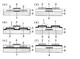
図1は、本発明に係る有機TFTの構成例を示す図である。同図(a)は、支持体6上に金属箔等によりソース電極2、ドレイン電極3を形成し、両電極間に本発明の有機半導体材料からなる有機半導体層1を形成し、その上に絶縁層5を形成し、更にその上にゲート電極4を形成して電界効果トランジスタを形成したものである。同図(b)は、有機半導体層1を、(a)では電極間に形成したものを、コート法等を用いて電極及び支持体表面全体を覆うように形成したものを表す。(c)は、支持体6上に先ずコート法等を用いて、有機半導体層1を形成し、その後ソース電極2、ドレイン電極3、絶縁層5、ゲート電極4を形成したものを表す。 FIG. 1 is a diagram showing a configuration example of an organic TFT according to the present invention. In FIG. 2A, a
同図(d)は、支持体6上にゲート電極4を金属箔等で形成した後、絶縁層5を形成し、その上に金属箔等で、ソース電極2及びドレイン電極3を形成し、該電極間に本発明の有機半導体材料により形成された有機半導体層1を形成する。その他同図(e)、(f)に示すような構成を取ることもできる。 In FIG. 4D, after forming the gate electrode 4 on the
図2は、有機TFTシートの概略等価回路図の1例を示す図である。 FIG. 2 is a diagram showing an example of a schematic equivalent circuit diagram of an organic TFT sheet.
有機TFTシート10はマトリクス配置された多数の有機TFT11を有する。7は各TFT11のゲートバスラインであり、8は各TFT11のソースバスラインである。各TFT11のソース電極には、出力素子12が接続され、この出力12は例えば液晶、電気泳動素子等であり、表示装置における画素を構成する。画素電極は光センサの入力電極として用いてもよい。図示の例では、出力素子として液晶が、抵抗とコンデンサからなる等価回路で示されている。13は蓄積コンデンサ、14は垂直駆動回路、15は水平駆動回路である。 The
以下、実施例により本発明を説明するが、本発明はこれらに限定されない。また、実施例に用いる比較化合物(2)の構造を下記に示す。 EXAMPLES Hereinafter, although an Example demonstrates this invention, this invention is not limited to these. Moreover, the structure of the comparative compound (2) used for an Example is shown below.
実施例1
《化合物(1)の合成》
化合物(1)を、J.Chem.Soc.,Perkin Trans.1,2000,1211−1216に従って合成し、チオフェン環を12単位含み、且つ、Head−to−Tail構造(HT構造)を有することを1H−NMRであることを確認した。また、HPLCの測定結果より99%以上の純度(この結果は、単一分子量成分の含有量がほほ100モル%であることを示している)であることを確認した。Example 1
<< Synthesis of Compound (1) >>
Compound (1) is prepared according to J. Am. Chem. Soc. Perkin Trans. It was synthesized according to 1,2000, 1211-1216, and it was confirmed by1 H-NMR that it contained 12 units of thiophene ring and had a Head-to-Tail structure (HT structure). Further, it was confirmed from the HPLC measurement result that the purity was 99% or more (this result indicates that the content of the single molecular weight component is almost 100 mol%).
《化合物(2)〜(5)、比較化合物(2)の合成》
化合物(1)の合成条件を参考にして、化合物(2)〜化合物(5)、比較化合物(2)(比較化合物(2)の単環であるチオフェン環の合計数は6である)についても同様に合成した。<< Synthesis of Compounds (2) to (5) and Comparative Compound (2) >>
With reference to the synthesis conditions of compound (1), compounds (2) to (5) and comparative compound (2) (the total number of thiophene rings, which are monocycles of comparative compound (2), is 6) It synthesized similarly.
《比較試料(3)の調製》
上記で合成した、化合物(1)〜化合物(5)の各々を等モル量混合して、比較化合物(3)を調製した。(単一分子量成分の含有量が各々20モル%となる。)
実施例2
《有機薄膜トランジスタ(有機TFT)素子1の作製》
ゲート電極としての比抵抗0.01Ω・cmのSiウェハーに、厚さ2000Åの熱酸化膜を形成してゲート絶縁層とした後、オクタデシルトリクロロシランによる表面処理を行った。比較化合物(1)(ポリ(3−ヘキシルチオフェン)(regio regular、アルドリッチ社製、平均分子量89000、PHT))のクロロホルム溶液をアプリケーターを用いて塗布し、自然乾燥することによりキャスト膜(厚さ50nm)を形成して、窒素雰囲気下で50℃、30分間の熱処理を施した。更に、この膜の表面にマスクを用いて金を蒸着してソース電極およびドレイン電極を形成した。ソース電極およびドレイン電極は幅100μm、厚さ200nmで、チャネル幅W=3mm、チャネル長L=20μmの有機薄膜トランジスタ素子1を作製した。<< Preparation of Comparative Sample (3) >>
Each of the compounds (1) to (5) synthesized above was mixed in an equimolar amount to prepare a comparative compound (3). (The content of each single molecular weight component is 20 mol%.)
Example 2
<< Production of Organic Thin Film Transistor (Organic TFT)
A Si oxide having a specific resistance of 0.01 Ω · cm as a gate electrode was formed with a thermal oxide film having a thickness of 2000 mm to form a gate insulating layer, and then surface treatment with octadecyltrichlorosilane was performed. A cast film (
《有機薄膜トランジスタ素子2、3の作製》
有機薄膜トランジスタ素子1の作製において、比較化合物(1)を比較化合物(2)、比較試料(3)に各々変更した以外は同様にして、有機薄膜トランジスタ素子2、3を各々作製した。<< Production of Organic Thin
Organic thin-
《有機薄膜トランジスタ素子4〜7の作製》
有機薄膜トランジスタ1の作製において、比較化合物(1)を表1に示した、本発明の有機半導体材料に各々変更した以外は同様にして、有機薄膜トランジスタ素子4〜7を各々作製した。尚、本発明の例示化合物のHPLC純度は、各々99%以上であった。<< Production of Organic Thin Film Transistor Elements 4-7 >>
In the production of the organic
《有機薄膜トランジスタ素子1〜7の評価》
有機薄膜トランジスタ素子1〜7は、pチャネルのエンハンスメント型FETの良好な動作特性を示した。ついで、前記有機薄膜トランジスタ素子1〜7について、I−V特性の飽和領域からキャリア移動度を求め、更にON/OFF比(ドレインバイアス−50Vとし、ゲートバイアス−50Vおよび0Vにしたときのドレイン電流値の比率)を求めた。また、得られた素子を大気中で1ヶ月放置し、再度キャリア移動度とON/OFF比を求めた。<< Evaluation of Organic Thin Film Transistor Elements 1-7 >>
The organic thin
得られた結果を表1に示す。 The obtained results are shown in Table 1.
表1の結果より、比較に比べて、本発明の有機薄膜トランジスタ素子は、トランジスタとしての特性が良好であり、さらに、経時劣化が抑えられていることが分かった。 From the results shown in Table 1, it was found that the organic thin film transistor element of the present invention had better characteristics as a transistor and further suppressed deterioration over time as compared with the comparison.
1 有機半導体層
2 ソース電極
3 ドレイン電極
4 ゲート電極
5 絶縁層
6 支持体
7 ゲートバスライン
8 ソースバスライン
10 有機TFTシート
11 有機TFT
12 出力素子
13 蓄積コンデンサ
14 垂直駆動回路
15 水平駆動回路DESCRIPTION OF
12 Output element 13 Storage capacitor 14 Vertical drive circuit 15 Horizontal drive circuit
Claims (12)
Translated fromJapanese該有機電荷輸送性材料が請求項1〜9のいずれか1項に記載の有機半導体材料であることを特徴とする電界効果トランジスタ。An organic charge transporting material and a gate electrode directly or indirectly in contact with the organic charge transporting material, and by applying a charge between the gate electrode and the organic charge transporting material, the organic charge transporting property In a field effect transistor that controls the current in a material,
A field effect transistor, wherein the organic charge transporting material is the organic semiconductor material according to any one of claims 1 to 9.
Priority Applications (1)
| Application Number | Priority Date | Filing Date | Title |
|---|---|---|---|
| JP2005032739AJP2006219550A (en) | 2005-02-09 | 2005-02-09 | Organic semiconductor material, organic thin film transistor, field effect transistor, and switching element |
Applications Claiming Priority (1)
| Application Number | Priority Date | Filing Date | Title |
|---|---|---|---|
| JP2005032739AJP2006219550A (en) | 2005-02-09 | 2005-02-09 | Organic semiconductor material, organic thin film transistor, field effect transistor, and switching element |
Publications (1)
| Publication Number | Publication Date |
|---|---|
| JP2006219550Atrue JP2006219550A (en) | 2006-08-24 |
Family
ID=36982076
Family Applications (1)
| Application Number | Title | Priority Date | Filing Date |
|---|---|---|---|
| JP2005032739APendingJP2006219550A (en) | 2005-02-09 | 2005-02-09 | Organic semiconductor material, organic thin film transistor, field effect transistor, and switching element |
Country Status (1)
| Country | Link |
|---|---|
| JP (1) | JP2006219550A (en) |
Cited By (2)
| Publication number | Priority date | Publication date | Assignee | Title |
|---|---|---|---|---|
| JP2006232986A (en)* | 2005-02-24 | 2006-09-07 | Mitsubishi Chemicals Corp | Conductive polymer and organic electronic device and field effect transistor using the same |
| JP2009040857A (en)* | 2007-08-08 | 2009-02-26 | Hiroshima Univ | Polythiophene and electroluminescent materials |
Citations (7)
| Publication number | Priority date | Publication date | Assignee | Title |
|---|---|---|---|---|
| JPH10190001A (en)* | 1996-12-20 | 1998-07-21 | Lucent Technol Inc | Manufacturing method of organic thin film transistor |
| JP2000230040A (en)* | 1999-02-10 | 2000-08-22 | Carnegie Mellon Univ | Method for producing poly (3-substituted thiophene) |
| JP2001196664A (en)* | 2000-01-12 | 2001-07-19 | Japan Science & Technology Corp | Photocarrier generation and transport material thin films for photoelectric conversion devices based on stereoregular polythiophene derivatives |
| JP2003261654A (en)* | 2002-03-07 | 2003-09-19 | Mitsubishi Chemicals Corp | Conductive polymer and method for producing the same, and electro-optical conversion device, electro-electronic device, photo-electric conversion device, and electric wiring board containing conductive polymer |
| JP2003292588A (en)* | 2002-01-11 | 2003-10-15 | Xerox Corp | Polythiophenes and devices using the same |
| JP2004115695A (en)* | 2002-09-27 | 2004-04-15 | Japan Science & Technology Corp | Method for producing poly (3-substituted thiophene) |
| JP2004339193A (en)* | 2003-03-07 | 2004-12-02 | Merck Patent Gmbh | Monomers, oligomers and polymers containing fluorene and aryl groups |
- 2005
- 2005-02-09JPJP2005032739Apatent/JP2006219550A/enactivePending
Patent Citations (7)
| Publication number | Priority date | Publication date | Assignee | Title |
|---|---|---|---|---|
| JPH10190001A (en)* | 1996-12-20 | 1998-07-21 | Lucent Technol Inc | Manufacturing method of organic thin film transistor |
| JP2000230040A (en)* | 1999-02-10 | 2000-08-22 | Carnegie Mellon Univ | Method for producing poly (3-substituted thiophene) |
| JP2001196664A (en)* | 2000-01-12 | 2001-07-19 | Japan Science & Technology Corp | Photocarrier generation and transport material thin films for photoelectric conversion devices based on stereoregular polythiophene derivatives |
| JP2003292588A (en)* | 2002-01-11 | 2003-10-15 | Xerox Corp | Polythiophenes and devices using the same |
| JP2003261654A (en)* | 2002-03-07 | 2003-09-19 | Mitsubishi Chemicals Corp | Conductive polymer and method for producing the same, and electro-optical conversion device, electro-electronic device, photo-electric conversion device, and electric wiring board containing conductive polymer |
| JP2004115695A (en)* | 2002-09-27 | 2004-04-15 | Japan Science & Technology Corp | Method for producing poly (3-substituted thiophene) |
| JP2004339193A (en)* | 2003-03-07 | 2004-12-02 | Merck Patent Gmbh | Monomers, oligomers and polymers containing fluorene and aryl groups |
Cited By (2)
| Publication number | Priority date | Publication date | Assignee | Title |
|---|---|---|---|---|
| JP2006232986A (en)* | 2005-02-24 | 2006-09-07 | Mitsubishi Chemicals Corp | Conductive polymer and organic electronic device and field effect transistor using the same |
| JP2009040857A (en)* | 2007-08-08 | 2009-02-26 | Hiroshima Univ | Polythiophene and electroluminescent materials |
Similar Documents
| Publication | Publication Date | Title |
|---|---|---|
| JP2007067263A (en) | Organic semiconductor material, organic semiconductor film, organic semiconductor device, and organic thin film transistor | |
| JP2005206750A (en) | Organic semiconductor materials, organic transistors, field effect transistors, switching elements, and 5-membered heterocyclic compounds | |
| JP2007088222A (en) | Organic semiconductor material, organic semiconductor film, organic semiconductor device, and organic thin film transistor | |
| JPWO2006059486A1 (en) | Organic thin film transistor material, organic thin film transistor, field effect transistor, switching element, organic semiconductor material, and organic semiconductor film | |
| JP2007019294A (en) | Organic semiconductor material, organic semiconductor film, organic semiconductor element, and organic thin film transistor | |
| JP2007088016A (en) | Organic semiconductor material, organic semiconductor film, organic semiconductor device, organic thin-film transistor, and organic electroluminescent element | |
| JPWO2005122278A1 (en) | Organic semiconductor thin film, organic semiconductor device, organic thin film transistor, and organic electroluminescence element | |
| JPWO2005122277A1 (en) | Organic thin film transistor | |
| JP2006216814A (en) | Organic semiconductor material, organic semiconductor thin film, organic thin film transistor, field effect transistor, and switching element | |
| JP5228907B2 (en) | Organic semiconductor material, organic semiconductor film, organic semiconductor device, and organic thin film transistor | |
| JP4992202B2 (en) | Organic semiconductor material, organic semiconductor film, organic thin film transistor, organic semiconductor film manufacturing method, and organic thin film transistor manufacturing method | |
| JPWO2005070994A1 (en) | Organic semiconductor materials, organic transistors, field effect transistors, switching elements, and thiazole compounds | |
| JP2007067262A (en) | Organic semiconductor material, organic semiconductor film, organic semiconductor device and organic semiconductor thin-film transistor | |
| JP2007311609A (en) | Material, film, and device for organic semiconductor and organic thin-film transistor | |
| JP2007317984A (en) | Organic semiconductor material, organic semiconductor film, organic semiconductor device, and organic thin film transistor | |
| JP2006339577A (en) | Organic semiconductor thin film and organic thin film transistor | |
| JP2007088224A (en) | Organic semiconductor material and organic semiconductor film using same, organic semiconductor device, and organic thin-film transistor | |
| JP2006060116A (en) | Organic thin film transistor material, organic thin film transistor, field effect transistor and switching element | |
| JPWO2006098121A1 (en) | Organic semiconductor material, organic semiconductor film, organic semiconductor device, organic thin film transistor, and method for forming organic thin film transistor | |
| JP2007088115A (en) | Organic semiconductor material, organic semiconductor film, organic semiconductor device, and organic thin-film transistor | |
| JP5157053B2 (en) | Organic semiconductor material, organic semiconductor film, organic semiconductor device, and organic thin film transistor | |
| JP2006140180A (en) | Organic thin film transistor material, organic thin film transistor, field effect transistor and switching element | |
| JP2006165015A (en) | Organic thin film transistor material, organic thin film transistor, field effect transistor and switching element | |
| JP2006222251A (en) | Organic semiconductor material, organic thin film transistor, field effect transistor, and switching element | |
| JPWO2006038459A1 (en) | Organic thin film transistor material, organic thin film transistor, field effect transistor and switching element |
Legal Events
| Date | Code | Title | Description |
|---|---|---|---|
| A621 | Written request for application examination | Free format text:JAPANESE INTERMEDIATE CODE: A621 Effective date:20080124 | |
| A977 | Report on retrieval | Free format text:JAPANESE INTERMEDIATE CODE: A971007 Effective date:20100310 | |
| A131 | Notification of reasons for refusal | Free format text:JAPANESE INTERMEDIATE CODE: A131 Effective date:20100427 | |
| A521 | Request for written amendment filed | Free format text:JAPANESE INTERMEDIATE CODE: A523 Effective date:20100625 | |
| A02 | Decision of refusal | Free format text:JAPANESE INTERMEDIATE CODE: A02 Effective date:20110419 |