JP2006216935A - Wafer level image sensor module and manufacturing method thereof - Google Patents
Wafer level image sensor module and manufacturing method thereofDownload PDFInfo
- Publication number
- JP2006216935A JP2006216935AJP2005351388AJP2005351388AJP2006216935AJP 2006216935 AJP2006216935 AJP 2006216935AJP 2005351388 AJP2005351388 AJP 2005351388AJP 2005351388 AJP2005351388 AJP 2005351388AJP 2006216935 AJP2006216935 AJP 2006216935A
- Authority
- JP
- Japan
- Prior art keywords
- image sensor
- wafer
- glass
- pad
- sensor module
- Prior art date
- Legal status (The legal status is an assumption and is not a legal conclusion. Google has not performed a legal analysis and makes no representation as to the accuracy of the status listed.)
- Pending
Links
Images


Classifications
- H—ELECTRICITY
- H10—SEMICONDUCTOR DEVICES; ELECTRIC SOLID-STATE DEVICES NOT OTHERWISE PROVIDED FOR
- H10F—INORGANIC SEMICONDUCTOR DEVICES SENSITIVE TO INFRARED RADIATION, LIGHT, ELECTROMAGNETIC RADIATION OF SHORTER WAVELENGTH OR CORPUSCULAR RADIATION
- H10F39/00—Integrated devices, or assemblies of multiple devices, comprising at least one element covered by group H10F30/00, e.g. radiation detectors comprising photodiode arrays
- H10F39/80—Constructional details of image sensors
- H10F39/806—Optical elements or arrangements associated with the image sensors
- H—ELECTRICITY
- H10—SEMICONDUCTOR DEVICES; ELECTRIC SOLID-STATE DEVICES NOT OTHERWISE PROVIDED FOR
- H10F—INORGANIC SEMICONDUCTOR DEVICES SENSITIVE TO INFRARED RADIATION, LIGHT, ELECTROMAGNETIC RADIATION OF SHORTER WAVELENGTH OR CORPUSCULAR RADIATION
- H10F39/00—Integrated devices, or assemblies of multiple devices, comprising at least one element covered by group H10F30/00, e.g. radiation detectors comprising photodiode arrays
- H10F39/10—Integrated devices
- H10F39/12—Image sensors
- H—ELECTRICITY
- H01—ELECTRIC ELEMENTS
- H01L—SEMICONDUCTOR DEVICES NOT COVERED BY CLASS H10
- H01L23/00—Details of semiconductor or other solid state devices
- H01L23/48—Arrangements for conducting electric current to or from the solid state body in operation, e.g. leads, terminal arrangements ; Selection of materials therefor
- H—ELECTRICITY
- H04—ELECTRIC COMMUNICATION TECHNIQUE
- H04N—PICTORIAL COMMUNICATION, e.g. TELEVISION
- H04N23/00—Cameras or camera modules comprising electronic image sensors; Control thereof
- H04N23/57—Mechanical or electrical details of cameras or camera modules specially adapted for being embedded in other devices
- H—ELECTRICITY
- H10—SEMICONDUCTOR DEVICES; ELECTRIC SOLID-STATE DEVICES NOT OTHERWISE PROVIDED FOR
- H10F—INORGANIC SEMICONDUCTOR DEVICES SENSITIVE TO INFRARED RADIATION, LIGHT, ELECTROMAGNETIC RADIATION OF SHORTER WAVELENGTH OR CORPUSCULAR RADIATION
- H10F39/00—Integrated devices, or assemblies of multiple devices, comprising at least one element covered by group H10F30/00, e.g. radiation detectors comprising photodiode arrays
- H10F39/011—Manufacture or treatment of image sensors covered by group H10F39/12
- H—ELECTRICITY
- H10—SEMICONDUCTOR DEVICES; ELECTRIC SOLID-STATE DEVICES NOT OTHERWISE PROVIDED FOR
- H10F—INORGANIC SEMICONDUCTOR DEVICES SENSITIVE TO INFRARED RADIATION, LIGHT, ELECTROMAGNETIC RADIATION OF SHORTER WAVELENGTH OR CORPUSCULAR RADIATION
- H10F39/00—Integrated devices, or assemblies of multiple devices, comprising at least one element covered by group H10F30/00, e.g. radiation detectors comprising photodiode arrays
- H10F39/80—Constructional details of image sensors
- H10F39/804—Containers or encapsulations
- H—ELECTRICITY
- H10—SEMICONDUCTOR DEVICES; ELECTRIC SOLID-STATE DEVICES NOT OTHERWISE PROVIDED FOR
- H10F—INORGANIC SEMICONDUCTOR DEVICES SENSITIVE TO INFRARED RADIATION, LIGHT, ELECTROMAGNETIC RADIATION OF SHORTER WAVELENGTH OR CORPUSCULAR RADIATION
- H10F77/00—Constructional details of devices covered by this subclass
- H10F77/40—Optical elements or arrangements
- H10F77/407—Optical elements or arrangements indirectly associated with the devices
- H—ELECTRICITY
- H10—SEMICONDUCTOR DEVICES; ELECTRIC SOLID-STATE DEVICES NOT OTHERWISE PROVIDED FOR
- H10F—INORGANIC SEMICONDUCTOR DEVICES SENSITIVE TO INFRARED RADIATION, LIGHT, ELECTROMAGNETIC RADIATION OF SHORTER WAVELENGTH OR CORPUSCULAR RADIATION
- H10F77/00—Constructional details of devices covered by this subclass
- H10F77/50—Encapsulations or containers
- H—ELECTRICITY
- H01—ELECTRIC ELEMENTS
- H01L—SEMICONDUCTOR DEVICES NOT COVERED BY CLASS H10
- H01L2224/00—Indexing scheme for arrangements for connecting or disconnecting semiconductor or solid-state bodies and methods related thereto as covered by H01L24/00
- H01L2224/01—Means for bonding being attached to, or being formed on, the surface to be connected, e.g. chip-to-package, die-attach, "first-level" interconnects; Manufacturing methods related thereto
- H01L2224/02—Bonding areas; Manufacturing methods related thereto
- H01L2224/04—Structure, shape, material or disposition of the bonding areas prior to the connecting process
- H01L2224/05—Structure, shape, material or disposition of the bonding areas prior to the connecting process of an individual bonding area
- H01L2224/05001—Internal layers
- H01L2224/0502—Disposition
- H01L2224/05026—Disposition the internal layer being disposed in a recess of the surface
- H—ELECTRICITY
- H01—ELECTRIC ELEMENTS
- H01L—SEMICONDUCTOR DEVICES NOT COVERED BY CLASS H10
- H01L2224/00—Indexing scheme for arrangements for connecting or disconnecting semiconductor or solid-state bodies and methods related thereto as covered by H01L24/00
- H01L2224/01—Means for bonding being attached to, or being formed on, the surface to be connected, e.g. chip-to-package, die-attach, "first-level" interconnects; Manufacturing methods related thereto
- H01L2224/02—Bonding areas; Manufacturing methods related thereto
- H01L2224/04—Structure, shape, material or disposition of the bonding areas prior to the connecting process
- H01L2224/05—Structure, shape, material or disposition of the bonding areas prior to the connecting process of an individual bonding area
- H01L2224/0554—External layer
- H01L2224/05541—Structure
- H01L2224/05548—Bonding area integrally formed with a redistribution layer on the semiconductor or solid-state body
- H—ELECTRICITY
- H01—ELECTRIC ELEMENTS
- H01L—SEMICONDUCTOR DEVICES NOT COVERED BY CLASS H10
- H01L2224/00—Indexing scheme for arrangements for connecting or disconnecting semiconductor or solid-state bodies and methods related thereto as covered by H01L24/00
- H01L2224/01—Means for bonding being attached to, or being formed on, the surface to be connected, e.g. chip-to-package, die-attach, "first-level" interconnects; Manufacturing methods related thereto
- H01L2224/10—Bump connectors; Manufacturing methods related thereto
- H01L2224/15—Structure, shape, material or disposition of the bump connectors after the connecting process
- H01L2224/16—Structure, shape, material or disposition of the bump connectors after the connecting process of an individual bump connector
- H01L2224/161—Disposition
- H01L2224/16151—Disposition the bump connector connecting between a semiconductor or solid-state body and an item not being a semiconductor or solid-state body, e.g. chip-to-substrate, chip-to-passive
- H01L2224/16221—Disposition the bump connector connecting between a semiconductor or solid-state body and an item not being a semiconductor or solid-state body, e.g. chip-to-substrate, chip-to-passive the body and the item being stacked
- H01L2224/16225—Disposition the bump connector connecting between a semiconductor or solid-state body and an item not being a semiconductor or solid-state body, e.g. chip-to-substrate, chip-to-passive the body and the item being stacked the item being non-metallic, e.g. insulating substrate with or without metallisation
- H01L2224/16238—Disposition the bump connector connecting between a semiconductor or solid-state body and an item not being a semiconductor or solid-state body, e.g. chip-to-substrate, chip-to-passive the body and the item being stacked the item being non-metallic, e.g. insulating substrate with or without metallisation the bump connector connecting to a bonding area protruding from the surface of the item
- H—ELECTRICITY
- H01—ELECTRIC ELEMENTS
- H01L—SEMICONDUCTOR DEVICES NOT COVERED BY CLASS H10
- H01L2924/00—Indexing scheme for arrangements or methods for connecting or disconnecting semiconductor or solid-state bodies as covered by H01L24/00
- H01L2924/01—Chemical elements
- H01L2924/01046—Palladium [Pd]
- H—ELECTRICITY
- H01—ELECTRIC ELEMENTS
- H01L—SEMICONDUCTOR DEVICES NOT COVERED BY CLASS H10
- H01L2924/00—Indexing scheme for arrangements or methods for connecting or disconnecting semiconductor or solid-state bodies as covered by H01L24/00
- H01L2924/01—Chemical elements
- H01L2924/01077—Iridium [Ir]
- H—ELECTRICITY
- H01—ELECTRIC ELEMENTS
- H01L—SEMICONDUCTOR DEVICES NOT COVERED BY CLASS H10
- H01L2924/00—Indexing scheme for arrangements or methods for connecting or disconnecting semiconductor or solid-state bodies as covered by H01L24/00
- H01L2924/01—Chemical elements
- H01L2924/01078—Platinum [Pt]
- H—ELECTRICITY
- H01—ELECTRIC ELEMENTS
- H01L—SEMICONDUCTOR DEVICES NOT COVERED BY CLASS H10
- H01L2924/00—Indexing scheme for arrangements or methods for connecting or disconnecting semiconductor or solid-state bodies as covered by H01L24/00
- H01L2924/01—Chemical elements
- H01L2924/01079—Gold [Au]
- H—ELECTRICITY
- H01—ELECTRIC ELEMENTS
- H01L—SEMICONDUCTOR DEVICES NOT COVERED BY CLASS H10
- H01L2924/00—Indexing scheme for arrangements or methods for connecting or disconnecting semiconductor or solid-state bodies as covered by H01L24/00
- H01L2924/15—Details of package parts other than the semiconductor or other solid state devices to be connected
- H01L2924/151—Die mounting substrate
- H01L2924/153—Connection portion
- H01L2924/1531—Connection portion the connection portion being formed only on the surface of the substrate opposite to the die mounting surface
- H01L2924/15311—Connection portion the connection portion being formed only on the surface of the substrate opposite to the die mounting surface being a ball array, e.g. BGA
- H—ELECTRICITY
- H01—ELECTRIC ELEMENTS
- H01L—SEMICONDUCTOR DEVICES NOT COVERED BY CLASS H10
- H01L2924/00—Indexing scheme for arrangements or methods for connecting or disconnecting semiconductor or solid-state bodies as covered by H01L24/00
- H01L2924/15—Details of package parts other than the semiconductor or other solid state devices to be connected
- H01L2924/151—Die mounting substrate
- H01L2924/153—Connection portion
- H01L2924/1532—Connection portion the connection portion being formed on the die mounting surface of the substrate
Landscapes
- Engineering & Computer Science (AREA)
- Multimedia (AREA)
- Signal Processing (AREA)
- Physics & Mathematics (AREA)
- Condensed Matter Physics & Semiconductors (AREA)
- General Physics & Mathematics (AREA)
- Computer Hardware Design (AREA)
- Microelectronics & Electronic Packaging (AREA)
- Power Engineering (AREA)
- Solid State Image Pick-Up Elements (AREA)
- Transforming Light Signals Into Electric Signals (AREA)
Abstract
Translated fromJapaneseDescription
Translated fromJapanese本発明はデジタル光学器機に用いられるウェーハレベルのイメージセンサーモジュール及びその製造方法に関するもので、より詳しくはCMOSあるいはCCDと呼ばれるイメージセンサーを具備したモジュールの大きさを小型化するためにその大きさを最小化し、良好な品質のイメージセンサーのみを選別して使用可能にすることにより、良好な品質のパッケージを生産して製作原価の節減を達することができ、大量生産に有利なウェーハレベルのイメージセンサーモジュール及びその製造方法に関するものである。 The present invention relates to a wafer level image sensor module used in a digital optical apparatus and a method of manufacturing the same, and more specifically, to reduce the size of a module having an image sensor called a CMOS or CCD. By minimizing and enabling the selection and use of only good quality image sensors, it is possible to produce good quality packages and achieve manufacturing cost savings, which is advantageous for mass production. The present invention relates to a module and a manufacturing method thereof.
近年、ポータブルまたは家庭用ビデオカメラとデジタルカメラのみならず、携帯電話のカメラ機能の採用によって超小型、高画質のイメージセンサーモジュールに対する要求が増えている。このようなイメージセンサーモジュールは優れた色再現性と微細な表現等の消費者要求による画素数増大のみならず、携帯電話の適用による軽薄短小の小型化及び高密度パッケージのイメージセンサーモジュールの必要性が高まっている状況である。 In recent years, not only portable or home video cameras and digital cameras, but also the demand for ultra-compact and high-quality image sensor modules due to the adoption of mobile phone camera functions has increased. Such an image sensor module not only increases the number of pixels due to consumer demands such as excellent color reproducibility and fine expression, but also the need for an image sensor module with light and thin size reduction and high density package by application of mobile phone The situation is growing.
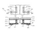
図1には、従来の技術によるウェーハレベルのイメージセンサーモジュール300の前面を表す。このような従来のウェーハレベルのイメージセンサーモジュール300は基本型構造として、携帯電話用カメラモジュールに適用される方式は大きく次の三種類の形態で、金ワイヤボンディング技術を利用したCOB(Chip On Board)、またはACF(Anisotropic Conductive Film)あるいは、NCP(Non−Conductive Paste)を利用したCOF(Chip On FPC)方式、そしてCSP(Chip Scale Package)方式に分類することができる。この中で最も注目を浴びているものは現在サイズが小さく、大量生産に適したCSPパッケージング方式である。 FIG. 1 illustrates a front surface of a conventional wafer level
このような従来のウェーハレベルのイメージセンサーモジュール及びその製造方法は様々な方式がある。その中でウェーハレベルのイメージセンサーモジュールで製造する方式はシェルケース社(SHELLCASE Ltd。)のSHELL-OPC方式が最も多く使用されている。 Such a conventional wafer level image sensor module and its manufacturing method have various methods. Among them, the SHELL-OPC method of SHELLCASE Ltd. is most often used as a method for manufacturing a wafer level image sensor module.
図1には、このような従来のSHELL−OPC方式のウェーハレベルのイメージセンサーモジュール300を示している。このような従来のウェーハレベルのイメージセンサーモジュール300は、WO99/40624号に記載されたもので、外部環境から保護され機械的な強度が補強された比較的薄く且つ稠密な構造を有するものであり、そのエッジ表面314に沿って多数の電気的接点312がメッキされている。 FIG. 1 shows a conventional SHELL-OPC wafer level
上記接点312は、エッジ表面全体にイメージセンサーモジュール300の平坦面316上に延長される。このような接点の配列を通してイメージセンサーモジュール300の平坦面と、エッジを回路基板に付着させることが可能となる。上記のような従来のウェーハレベルのイメージセンサーモジュール300は、融着性バンプ電極ら317が各接点312の端部に形成されているものを表す。上記融着性バンプ電極ら317は所定の隊形で配列される構造である。 The
図2には、上記と類似な従来のウェーハレベルのイメージセンサーモジュール350を示している。これはWO99/40624号に記載された内容として、上記ウェーハレベルのイメージセンサーモジュール350は、光放出機と光受信機中で少なくとも一つを具備し、上面と下面が電気的絶縁及び機械的保護物質から形成されており、その上面と下面中で少なくとも一つには保護膜357が光を透過し、電気的絶縁性であるエッジ表面364らがパッドを具備する集積回路ダイ372を含んでいる。 FIG. 2 shows a conventional wafer level
そこで、このような従来のウェーハレベルのイメージセンサーモジュール350は、そのエッジ表面364に沿って多数の電気的接点382がメッキされており、選別フィルター及び/又は反射防止コーティング膜395が透明保護膜357の外部接合面356に形成されている構造である。 Therefore, in the conventional wafer level
図3には、さらに他の構造の従来ウェーハレベルのイメージセンサーモジュール400を示している。これはWO01/43181号に記載された内容として、結晶質のシリコン基材に形成されたマイクロレンズアレイ410を具備する。上記シリコン基材412の下には通常ガラスから形成されたパッケージ層416がエポキシ414によって密封されているが、該パッケージ層416のエッジに沿って電気コンタクト428が形成され、該電気コンタクト428は通常バンプ電極430を形成する。そして、導電性パッド432は上記シリコン基材412を電気コンタクト428に連結させる。 FIG. 3 shows a conventional wafer level
このような従来のウェーハレベルのイメージセンサーモジュール400は、通常ガラス層444とこれに係わるスペーサ要素436らがシリコン基材412の上部にエポキシ438などの接着剤で密封されてマイクロレンズアレイ410とガラス層444の間に空間446が形成できるようになる。上記パッケージ層444は好ましくは透明なものである。 In such a conventional wafer level
一方、図4には上記とは異なる方式のウェーハレベルのイメージセンサーモジュール450を示している。これは日本国特許出願第2002-274807号に記載された内容として、複数のイメージセンサーモジュールに対応するサイズのガラス基板459上に透明接着層458が付着され、その上には下面に光電変換デバイス領域452を有するシリコン基板451が互いに間隙を形成しながら接着されている。このような従来の構造は、シリコン基板451の下面周辺部及びその周りに接続用配線457がシリコン基板451の接続パッド453に接続されている。 On the other hand, FIG. 4 shows a wafer level
そして、絶縁膜456、再配線461、柱状電極462、封止膜463及び溶接ボール464を形成した後に、シリコン基板451の間を切断し、光電変換デバイス領域452を具備したウェーハレベルのイメージセンサーモジュール450を複数個得る。しかしながら、このようなウェーハレベルのイメージセンサーモジュール450はその構造が複雑なため製作しにくい問題点がある。 Then, after forming the insulating film 456, the rewiring 461, the
一方、図5には上記とはさらに異なる従来のウェーハレベルのイメージセンサーモジュール500が示している。これは日本国特許公開第2004-153260号に記載された内容として、半導体チップ510上に形成されるパッド電極511と、上記半導体チップ510の表面に接着される支持基板513を具備し、上記半導体チップ510の裏面から上記パッド電極511の表面に到達するようビアホール517が形成され、上記ビアホール517内に上記パッド電極511と接続される柱状端子520が形成される。 On the other hand, FIG. 5 shows a conventional wafer level
さらに、上記柱状端子520には再配線層521が形成され、その再配線層521上にはソルダマスク522が被覆され、バンプ電極523が上記再配線層521に電気的に連結される構造である。 Further, a rewiring
このような従来の技術は、その独特な構造によって断線やステップカバレージの劣化を防止し、信頼性の高いBGAを有するウェーハレベルのイメージセンサーモジュール500を提供しようとしたのである。 Such a conventional technique is intended to provide a wafer level
しかし、上記のような従来のイメージセンサーモジュールらは装着されるイメージセンサーの収率が著しく低い時に問題点を有するもので、このような方式はウェーハレベルのイメージセンサーモジュールを生産する過程において不良品であるアウトダイ(Out Die)のイメージセンサーまでパッケージングをするようになるので、アウトダイのイメージセンサーらをパッケージングする費用も良品のグットダイ(Good Die)のイメージセンサーらをパッケージングする費用に含まれ生産原価が高くなる問題点を有する。 However, the conventional image sensor modules as described above have problems when the yield of the mounted image sensor is extremely low, and such a method is a defective product in the process of producing a wafer level image sensor module. Since the packaging of out-die image sensors is also included, the cost of packaging out-die image sensors is also included in the cost of packaging good-good image sensors. There is a problem that the production cost becomes high.
さらに、図6のa、bにはさらに他の従来のウェーハレベルのイメージセンサーモジュール600が図示している。これはガラス層(Glass)を使用してガラス基板605にして、その上に金属配線610とこれを保護するための絶縁膜612を形成し、イメージセンサーチップ(Image Sensor Chip)620とガラス基板605をソルダボールジョイント(Solder ball Joint)630を利用して電気的に連結したものである。 6A and 6B show still another conventional wafer level
また、上記金属配線610には外側ソルダボール(Outer Solder Ball)640らが形成されて外部のPCB基板(図示せず)に電気的に連結可能になるよう構成される。 The
従って、イメージセンサーチップ(Image Sensor Chip)620からの電気的信号がガラス基板605上の金属配線610と外側ソルダボール(Outer Solder Ball)を通して外部PCB基板に伝達される方式である。 Accordingly, an electrical signal from the image sensor chip (Image Sensor Chip) 620 is transmitted to the external PCB substrate through the
しかし、上記のような従来のイメージセンサーモジュールはその構造が複雑で、製作しにくい問題点を有するのである。 However, the conventional image sensor module as described above has a complicated structure and is difficult to manufacture.
また、上記のような従来のウェーハモジュールのイメージセンサーモジュールらが受光する光はその波長が赤外線領域、可視光線領域、紫外線領域などその以外の領域らもあるが、人が物を見て認識する波長領域の可視光線領域を含む。 Further, the light received by the image sensor modules of the conventional wafer module as described above has other wavelengths such as an infrared region, a visible light region, an ultraviolet region, etc., but a person sees and recognizes the object. Includes the visible light region in the wavelength region.
従って、上記のような従来のイメージセンサーモジュールを装着するカメラモジュールは光学フィルターを内蔵しているが、このような光学フィルターがIRフィルターの場合は赤外線透過率を下げる。上記赤外線領域の光は熱を含んでいるので上記光学フィルターを通してその透過率を下げ、反射率を上げて上記光を受光するイメージセンサーを保護し、人が認識する可視光線領域の透過率を上げる役割をするようになる。 Accordingly, the camera module to which the conventional image sensor module as described above is mounted has an optical filter, but when such an optical filter is an IR filter, the infrared transmittance is lowered. Since the light in the infrared region contains heat, the transmittance is lowered through the optical filter, the reflectance is increased to protect the image sensor that receives the light, and the transmittance in the visible light region recognized by humans is increased. Comes to play a role.
従来には光学フィルターを四角のガラスにコーティングしてこれをばらにカッティングし、これをそれぞれのイメージセンサーモジュールに付着する方式である。 Conventionally, an optical filter is coated on a square glass, and this is cut into pieces, and this is attached to each image sensor module.
従って、従来にはカメラモジュールに上記のようなイメージセンサーモジュールを装着することとは別に光学フィルターを装着するものであるので、その作業工程は多段階に行なわれるものであり、それによって工程改善が必要な問題点を有したのである。 Therefore, conventionally, since the optical filter is mounted separately from the mounting of the image sensor module as described above on the camera module, the work process is performed in multiple stages, thereby improving the process. It had the necessary problems.
上記のような従来の問題点を解消するために、本発明はガラスウェーハに良品のイメージセンサーのみ実装してパッケージングするようになることによりイメージセンサーモジュールの収率を画期的に上げることができ、それによる生産原価の節減は勿論、大量生産に有利なウェーハレベルのイメージセンサーモジュール及びその製造方法を提供することに目的がある。 In order to solve the conventional problems as described above, the present invention can dramatically increase the yield of an image sensor module by mounting only a good image sensor on a glass wafer and packaging. It is possible to provide a wafer level image sensor module and a method for manufacturing the same that are advantageous for mass production, as well as saving production costs.
本発明の他の目的は、その製造工程において光学フィルターを一体で形成することができるのでカメラモジュールに別途の光学フィルターを付着しなくても良いことから、作業工程の改善による作業生産性の向上を達することができるウェーハレベルのイメージセンサーモジュール及びその製造方法を提供することに目的がある。 Another object of the present invention is that the optical filter can be integrally formed in the manufacturing process, so that it is not necessary to attach a separate optical filter to the camera module. It is an object of the present invention to provide a wafer level image sensor module capable of achieving the above and a manufacturing method thereof.
また、本発明のさらに他の目的はPCBに装着する工程において、従来の実装方式であるリフローを通じても簡単に実装することができるので、カメラモジュールの組み立て作業の生産性を著しく向上させることが可能であるイメージセンサーモジュール及びその製造方法を提供することに目的がある。 Another object of the present invention is that it can be easily mounted through reflow, which is a conventional mounting method, in the process of mounting on the PCB, so that the productivity of the assembly work of the camera module can be remarkably improved. It is an object to provide an image sensor module and a manufacturing method thereof.
上記のような目的を成し遂げるために本発明は、デジタル器機等に用いられるウェーハレベルのイメージセンサーモジュールにおいて、上記イメージセンサーに流入される光から特定波長を除去させる光学フィルター、上記光学フィルターに付着されてフィルターコーティング層を保護し、その後面にはパッド電極らが形成されるガラス層、及び上記ガラス層のパッド電極に付着され、上記パッド電極からその後面に再分配パッドが形成されるイメージセンサー、及び上記イメージセンサーの後面側に配置され、上記パッド電極に電気的に連結されるソルダボール、らを含むことを特徴とするウェーハレベルのイメージセンサーモジュールを提供する。 In order to achieve the above object, the present invention is applied to an optical filter for removing a specific wavelength from light flowing into the image sensor in a wafer level image sensor module used in a digital instrument or the like, and the optical filter. An image sensor that protects the filter coating layer, a glass layer on which the pad electrode is formed on the rear surface, and an image sensor that is attached to the pad electrode of the glass layer and a redistribution pad is formed on the rear surface from the pad electrode; And a solder ball disposed on the rear side of the image sensor and electrically connected to the pad electrode.
さらに、本発明はデジタル器機等に用いられるウェーハレベルのイメージセンサーモジュールの製造方法において、上記イメージセンサーに流入される光から特定波長を除去させるウェーハ状光学フィルターとウェーハ状ガラス層を互いに接着してガラスウェーハを形成する段階、上記ガラスウェーハのガラス層にパッド電極を形成する段階、上記パッド電極にバンプ電極を接合させ多数のイメージセンサーをガラスウェーハに付着する段階、上記ガラスウェーハのパッド電極を各々のイメージセンサーの後面に形成して再分配パッドを形成する段階、上記イメージセンサーの再分配パッドの上に各々ソルダボールを形成する段階、及び上記ガラスウェーハを多数のイメージセンサーモジュールらで切断する段階、を含むことを特徴とするウェーハレベルのイメージセンサーモジュール製造方法を提供する。 Furthermore, the present invention relates to a method for manufacturing a wafer level image sensor module used in a digital instrument or the like, wherein a wafer-like optical filter for removing a specific wavelength from the light flowing into the image sensor and a wafer-like glass layer are bonded to each other. Forming a glass wafer; forming a pad electrode on a glass layer of the glass wafer; bonding a bump electrode to the pad electrode; and attaching a large number of image sensors to the glass wafer; Forming a redistribution pad on the rear surface of the image sensor, forming solder balls on the redistribution pad of the image sensor, and cutting the glass wafer with a plurality of image sensor modules. , Characterized by containing Providing an image sensor module manufacturing method of Hareberu.
本発明によれば、COBのワイヤボンディングやCOFのACF(Anisotropic Conductive Film)あるいは、NCP(Non−Conductive Paste)を利用したフリップチップバンプ電極連結を代替する方式であり、従来とは違ってイメージセンサー40のパッド電極30を再分配(Redistribution)してソルダボール70を付着することができるバンプ電極を形成するウェーハレベルのイメージセンサーモジュール1が提供される。 According to the present invention, a COB wire bonding, a COF ACF (Anisotropic Conductive Film), or a flip-chip bump electrode connection using NCP (Non-Conductive Paste) is used. A wafer level image sensor module 1 is provided that
そして、本発明はガラスウェーハ100を使用したイメージセンサーモジュール方式として、グットダイのみのイメージセンサー40らを選択し、これらをガラスウェーハ100にフリップチップボンディングして製作する方式である。従って、本発明ではグットダイのイメージセンサー40らのみを実装するので、イメージセンサー40らの不良によるウェーハレベルのイメージセンサーモジュール1の不良が生じられる問題点を解決することができる。 The present invention is a system in which an
また、ウェーハ状のガラス層20と光学フィルター10を付着したガラス100を使用して製作され、ガラスウェーハ100にイメージセンサー40をボンディングした後、樹脂で埋め込んで完全に密封をした後、ビアホール52らを樹脂に形成してソルダバンプ電極を形成して製作されるので、本発明によるウェーハレベルのイメージセンサーモジュール1をカメラモジュールに組み立てる場合、別途の光学フィルター10を付着する必要がない。従って、カメラモジュールの組み立て段階を画期的に単純化させることができ、大量生産が有利であり、生産原価の節減を達することができる效果が得られる。 Also, the
そして、本発明によればイメージセンサー40の大きさを最小化してカメラモジュールの大きさをより小さくすることができ、ウェーハレベルのイメージセンサーモジュール1の製作をウェーハレベル段階で行うので大量生産や生産原価の節減を達することができる長所がある。 According to the present invention, the size of the
のみならず、本発明はイメージセンサー40の後面(Back Side)を利用するので全体的なパッケージサイズを最小限に減らすことができ、連結リード(Connection Lid)をソルダボール70で形成するので異方性伝導性フィルムあるいは接着剤を使用しなくても通常のリフロー実装技術を通じて簡単にPCBに実装して軽薄短小のカメラモジュールを構成することが可能である。 In addition, since the present invention uses the rear surface (Back Side) of the
上記においては本発明の好ましき特定実施例に関して詳しく説明されたが、本発明はそれに限定されるわけではない。本明細書または図面の記載内容を通じて当業者らは上記実施例とは異なる本発明の変形構造または均等構造らを多様に構成することができるが、これらは全て本発明の技術思想内に含まれるものである。とりわけ、本発明の構成要素らの材質変更、単純機能の付加、単純形状変更または寸法変更等が様々に提示されることができるが、これらは全て本発明の権利範囲内に含まれるものであることは明らかである。 Although the foregoing has been a detailed description of the preferred specific embodiment of the invention, the invention is not so limited. Those skilled in the art can make various modifications and equivalent structures of the present invention different from the above-described embodiments through the description of this specification or the drawings, all of which are included in the technical idea of the present invention. Is. In particular, various changes in material, addition of simple functions, change in simple shape, or change in dimensions of the components of the present invention can be presented, all of which are included within the scope of the present invention. It is clear.
以下、本発明を図面を参照してより詳しく説明する事にする。 Hereinafter, the present invention will be described in more detail with reference to the drawings.
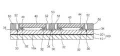
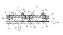
本発明によるウェーハレベルのイメージセンサーモジュール1は図7に示すように、イメージセンサーに流入される光から特定波長を除去させる光学フィルター10を一体で具備する。 As shown in FIG. 7, the wafer level image sensor module 1 according to the present invention integrally includes an
上記光学フィルター10は通常のIRフィルターからなることができるが、本発明はそれに限定されるものではない。上記光学フィルター10はそのコーティング層10aが上、下の両面に形成され得るが、好ましくは以後に説明されるガラス層20に向い合うように形成される。 The
そして、本発明によるウェーハレベルのイメージセンサーモジュール1は上記光学フィルター10に付着されフィルターコーティング層10aを保護し、その後面にはパッド電極30らが形成されるガラス層20を具備する。 The wafer level image sensor module 1 according to the present invention includes a
上記ガラス層20は光学フィルター10を透明な接着剤を使用して接着したり、空気中の水分を利用してH基とOH基でボンディングするフュージョンボンディング(Fusion Bonding)によって成ることができる。後者のフュージョンボンディングはガラス層20と光学フィルター10の間に何にもなしにボンディングが可能であるので、光の透過率が100%保障される。従って、透明な接着剤を使用する時よりもより良い光の透過特性を得ることができる。ここで、上記光学フィルター10のコーティング層10aは上記ガラス層20との間に形成されることが好ましい。 The
そして、上記ガラス層20はその外面にパッド電極30が形成されている。上記パッド電極30はPVD方式を利用してスパッタリングにTiW、 Al、Cu及びNiなどのような金属をシードメタルで使用可能であり、無電解メッキ方式にはPdのような金属が使用可能である。そして、シードメタル上の本メタルにはNiの上にAuが一般的であり、Cu、Sn及びSnの合金メッキが可能である。 The
メッキ方式にはシードメタルのようにPVD方式のスパッタリングが可能であるが、電気メッキを行った方が量産性の側面や大量生産に適する。また、上記パッド電極30は上記ガラス層20にコーティングされたメタルをパターニング(Paterning)して得るようになり、このように得られたパッド電極30は以後に説明されるイメージセンサー40とフリップチップ(Flip Chip)をボンディングするための対応フリップチップパッド32と、再分配のための拡張パッド34を含む。 The plating method can be PVD-type sputtering like seed metal, but electroplating is more suitable for mass productivity and mass production. Further, the
また、本発明によるウェーハレベルのイメージセンサーモジュール1は上記ガラス層20のパッド電極30に付着され、そのパッド電極30から再分配パッド42が後面に形成されるイメージセンサー40を具備する。 In addition, the wafer level image sensor module 1 according to the present invention includes an
上記イメージセンサー40はグットダイ(Good Die;良品のイメージセンサー)のみをフリップチップボンディングして結合されたものである。上記フリップチップボンディング方式のイメージセンサー40にはAuバンプ電極44を適用してACF(Antisotropic Conductive Film)でボンディングするのが一般的である。ここで、ACFをACP(Antisotropic Conductive Paste)、 NCP(Non−Conductive Paste)及びNCF(Non-Conductive Film)などでボンディングすることも可能である。また、イメージセンサー40のバンプ電極44をAuバンプ電極ではないソルダボールバンプ電極を適用することも可能である。 The
そして、本発明によるウェーハレベルのイメージセンサーモジュール1は上記イメージセンサー40の後面に形成される再分配パッド42が上記ガラス層20に形成されたパッド電極30の拡張パッド34に電気的に連結されるもので、上記拡張パッド34と再分配パッド42との間には絶縁樹脂層50が形成されて、上記絶縁樹脂層50を貫通するビアホール52らが形成され、その内部にメタルをメッキして上記拡張パッド34と再分配パッド42らが電気的に連結されるのである。 In the wafer level image sensor module 1 according to the present invention, the
また、本発明は上記イメージセンサー40の後面側に配置され、上記パッド電極30に電気的に連結されるソルダボール70らを含む。 Further, the present invention includes
このような構造を備えることにより、本発明によるウェーハレベルのイメージセンサーモジュール1は従来の方式で提起された問題点らを解決する。すなわち、従来方式のイメージセンサーモジュールにおいては、イメージセンサーがウェーハ状で製作完了(FAB OUT) されると、不良なイメージセンサーらを多量含んだ収率の低いイメージセンサーウェーハがイメージセンサーモジュールに生産される。このような場合、不良なイメージセンサーらが不良なイメージセンサーモジュールらを発生させ、結果的にこのような不良な多量のイメージセンサーモジュールらが廃棄され、それによってその費用がそっくりそのままイメージセンサーの品質が優れたグットダイの量品イメージセンサーモジュールに転嫁される。 By providing such a structure, the wafer level image sensor module 1 according to the present invention solves the problems raised in the conventional method. That is, in the conventional image sensor module, when the image sensor is manufactured in a wafer form (FAB OUT), a low yield image sensor wafer containing a large amount of defective image sensors is produced in the image sensor module. The In such a case, defective image sensors generate defective image sensor modules, and as a result, a large number of such defective image sensor modules are discarded, so that the cost of the image sensor remains unchanged. Is passed on to an excellent mass sensor image sensor module.
従って、従来には良好な品質のグットダイのイメージセンサーらを有する良好なイメージセンサーモジュールの生産費用が不可避的に上昇されるが、本発明においてはこれとは関係なく品質の優れたイメージセンサーのグットダイのみを選別して使用するので、このような問題点らを完全に解決することができるのである。 Therefore, the production cost of a good image sensor module having a good quality good die image sensor is inevitably increased in the past. However, in the present invention, the good quality image sensor good die is unrelated to this. Since these are selected and used, such problems can be completely solved.
そして、本発明によるウェーハレベルのイメージセンサーモジュール製造方法は先ず、図8a、bに示すように、上記イメージセンサー40に流入される光から特定波長を除去させるウェーハ状光学フィルター10とウェーハ状ガラス層20を互いに接着してガラスウェーハ100を形成する段階が行なわれる。 The wafer level image sensor module manufacturing method according to the present invention, first, as shown in FIGS. 8a and 8b, a wafer-like
本発明の一番目の段階はガラスをウェーハ状に加工して一方のガラス層20を形成し、他方のウェーハ状ガラスには光学フィルター用コーティング層10aを形成してウェーハ状の光学フィルター10を形成した後、これら二つをボンディングしてガラスウェーハ100を形成する段階である。 In the first stage of the present invention, the glass is processed into a wafer shape to form one
従来には四角のガラスにコーティング層を形成して光学フィルターをばらにカッティングし、それをカメラモジュールにそれぞれ付着して使用した。 Conventionally, a coating layer is formed on square glass, and an optical filter is cut into pieces, which are then attached to a camera module for use.
しかし、本発明においては従来の技術とは違って、光学フィルター10をウェーハ形態に構成して、ガラスウェーハ100を製作した後、上記ガラスウェーハ100をウェーハレベルとして製作段階らを進めパッケージングし、これをイメージセンサー40別に切断(Dicing)してそれぞれの多数個のウェーハレベルのイメージセンサーモジュール1を完成する。 However, in the present invention, unlike the prior art, after the
上記ガラスウェーハ100を形成する段階ではウェーハ形態のガラス層20とウェーハ型の光学フィルター10を付着する段階として、これらを図8bに示すような透明な接着剤16を使用して接着する方法があり、空気中の水分を利用してH基とOH基でボンディングするフュージョンボンディング(Fusion Bonding)がある。後者のフュージョンボンディングは上記ガラス層20と光学フィルター10の間に何もなしにボンディングが可能であるので光の透過率が100%保障される。従って、透明な接着剤16を使用する時よりもより良い光の透過特性を得ることができる。このようにガラス層20とウェーハ状光学フィルター10を接着してガラスウェーハ100を形成する。 In the step of forming the
そして、本発明によるウェーハレベルのイメージセンサーモジュール製造方法は上記ガラスウェーハ100のガラス層20にパッド電極30を形成する段階を含む。 The method for manufacturing a wafer level image sensor module according to the present invention includes a step of forming a
この段階は上記一番目の段階で製作されたガラスウェーハ100にパターニングを形成するためにメタルを被い段階を含む。このようにガラスウェーハ100のガラス層20にメタル102を形成する段階は図9に示すように、上記ガラス層20にシードメタルを被い、本メタルを被う。上記シードメタルはPVD(Physical Vapor Deposition)方式を利用してスパッタリングにTiW、Al、Cu及び Niなどのようなメタルをシードメタル(Seed Metal)で使用可能であり、無電解メッキ方式にはPdのようなメタルが使用可能である。上記本メタルにはNiの上にAuが一般的であり、Cu、Sn及びSnの合金メッキが可能である。メッキ方式にはシードメタルのようにPVD方式のスパッタリングが可能であるが、電気メッキを行う方が量産性側面や大量生産に適する。 This step includes a step of covering with metal to form a pattern on the
そして、上記ガラスウェーハ100のガラス層20にパッド電極30を形成する段階はガラスウェーハ100のガラス層20にコーティングされたメタル102をパターニングする段階である。上記パターニング段階は図10に示すように、ガラス層20に形成されたメタル102層にパターンを形成してイメージセンサー40とフリップチップボンディングしてイメージセンサー40を装着するためのフリップチップパッド32を形成し、以後に説明される再分配パッド42を形成するための拡張パッド34を形成する。 The step of forming the
これは図10に示すように、それぞれガラスウェーハ100のガラス層20にはイメージセンサー40が位置される領域110と、各々の上記領域110を包囲するようにフリップチップパッド32と拡張パッド34らが形成されるのである。 As shown in FIG. 10, the
また、本発明によるウェーハレベルのイメージセンサーモジュール製造方法は上記パッド電極30にバンプ電極44を接合させ多数のイメージセンサー40らをガラスウェーハ100に付着する段階を含む。 In addition, the wafer level image sensor module manufacturing method according to the present invention includes the step of bonding the
この段階においては、上記ガラスウェーハ100にグットダイ(Good Die;良品のイメージセンサー)のみをフリップチップボンディングする段階を含む。この段階は図11に示すように、予め形成されられたガラスウェーハ100のフリップチップパッド32にグットダイのイメージセンサー40に形成されたバンプ電極(bumps)44をボンディングする。上記フリップチップボンディング方式のイメージセンサー40にはAuバンプ電極を適用してACFでボンディングすることが一般的である。 This step includes the step of flip-chip bonding only the good die (good image sensor) to the
しかし、本発明はそれに限定されず、上記ACFをACP、NCP及びNCFなどに代替してボンディングすることができることは勿論である。また、イメージセンサー40のバンプ電極44をAuバンプ電極ではないソルダボールバンプ電極に代替して適用することも可能である。 However, the present invention is not limited to this, and it is needless to say that the ACF can be replaced by ACP, NCP, NCF, or the like. Further, the
上記のように本発明は、このような製造段階を含むことにより、不良なイメージセンサー40らを除去し、イメージセンサー40の品質が優れたグットダイ良品のイメージセンサー40のみを選別して装着することにより結果的にイメージセンサー40において不良が発生しない良好な品質のウェーハレベルのイメージセンサーモジュール1を得ることができる。 As described above, the present invention includes such a manufacturing stage to remove
従って、良好な品質のグットダイのイメージセンサー40らを有する良好なウェーハレベルのイメージセンサーモジュール1の生産費用が下がる效果を得ることができる。 Therefore, it is possible to obtain an effect of reducing the production cost of the good wafer level image sensor module 1 having the good quality good
そして、本発明によるウェーハレベルのイメージセンサーモジュール製造方法は上記ガラスウェーハ100のパッド電極30を各々のイメージセンサー40の後面(Back Side)に形成して再分配パッド42を形成する段階を含む。 The wafer level image sensor module manufacturing method according to the present invention includes a step of forming the
このように再分配パッド42を形成する段階は、先ず上記イメージセンサー40がフリップチップボンディングされたガラスウェーハ100にイメージセンサー40とセンサー40らの間の空間を樹脂層50で埋め込む段階を含む。上記樹脂層50を埋め込む段階は図12a、bに示すようにイメージセンサー40とセンサー40の間の空間を樹脂で均一に埋め込み、ベーキングして硬化させる。上記樹脂はエポキシ、BCB(Benzocyclobutene)などがある。 The step of forming the
そして、上記段階は図13に示すように、硬化された樹脂にビアホール52をエッチングする段階を含む。ここで、ビアホール52をエッチングする方法には様々な方法があり得る。例えば、フォトリソグラフィ段階としてマスクを利用して露光し、現像する方式でビアホール52をエッチングすることができ、レーザーやドライエッチング方法でビアホール52らをエッチングすることができる。 Then, as shown in FIG. 13, the step includes a step of etching the via
また、上記段階は上記のように硬化された樹脂層50に形成されたビアホール52らの内部にメタルをコーティングしたり、埋める方式を適用して拡張パッド34から電気的に連結されるようにイメージセンサー40の後面に再分配パッド42を形成するのである。 In addition, the above-described step is an image in which the metal is coated or buried in the via
この段階は図14に示すように、拡張パッド34をイメージセンサー40の後面に延長させ再分配パッド42を形成するもので、シードメタル(Seed Metal)をPVD方式やCVD(Chemical Vapor Deposition)方式または無電解方式で形成し、PVD方式や電気メッキ、コンダクティング材料等でメタルをビアホール52の内部に塗たり、埋め込むことができる。このように再分配パッド42を形成する段階はシリコーンウェーハをエッチングする方式より樹脂層50をエッチングする方式がはるかに容易であり、良い品質を得ることができる。 In this stage, as shown in FIG. 14, the
また、本発明によるウェーハレベルのイメージセンサーモジュール製造方法は上記イメージセンサー40の再分配パッド42上に各々ソルダボール70を形成する段階を含む。 In addition, the method of manufacturing a wafer level image sensor module according to the present invention includes forming
この段階は図15に示すように、上記イメージセンサー40の後面に形成された再分配パッド42上にソルダボール70を形成する段階である。このような段階は例えば、プリンティング方式でソルダボール70を上記再分配パッド42上に作ることができ、ソルダボール70のピッチの大きい場合はマスクを使用することができ、ピッチの微細な場合は感光性フィルムレジストを使用する方法にすることができる。 This step is a step of forming
本発明では電子機器の軽薄短小化の傾向でソルダボール70のピッチが継続して小さくなっており感光性フィルムレジストを使用するようになる。 In the present invention, the pitch of the
上記のようにソルダボール70を形成する方法は一般的に広く知られた技術であり、様々な方法があるので、ここではより詳しくは記述しない。 The method of forming the
また、本発明によるウェーハレベルのイメージセンサーモジュールの製造方法は最後に上記のような段階らを経て生産された上記ガラスウェーハ100を多数のウェーハレベルのイメージセンサーモジュール1らで切断する段階を含む。 In addition, the method for manufacturing a wafer level image sensor module according to the present invention includes a step of cutting the
この切断段階は図16に示すように、上記製造方法を通して完成されたガラスウェーハ100を多数個のばらのウェーハレベルのイメージセンサーモジュール1らでダイシング(Dicing)する段階である。このようなダイシング段階はイメージセンサーら毎に形成された拡張パッドらの間と間を切断し多数個の良好なウェーハレベルのイメージセンサーモジュール1らを生産するのである。 As shown in FIG. 16, the cutting step is a step of dicing the
このようにばらのチップ(Chip)に切られたウェーハレベルのイメージセンサーモジュール1らはカメラモジュールの組み立て段階において、予めイメージセンサー40の後面にソルダボール70らが形成されているので、一般的なリフロー段階を経て容易に組み立てが可能であり、それによってカメラモジュールを製作する段階において多数の段階を省くことができる。 Since the wafer level image sensor module 1 cut into loose chips (Chips) in this manner has
また、本発明によるウェーハレベルのイメージセンサーモジュール1はイメージセンサー40と共に光学フィルター10を一体で構成しているので、従来のカメラモジュールの製作段階に比して除去され得る段階は、光学フィルター10の準備段階として、光学フィルター10のばらカッティング、カッティング後の検査、そしてボンドディスぺンシング、光学フィルター10付着、及びUV硬化等の段階らを除去または省略することができる。 In addition, since the wafer level image sensor module 1 according to the present invention integrally forms the
1 本発明によるウェーハレベルのイメージセンサーモジュール
10 光学フィルター
10a コーティング層
20 ガラス層
30 パッド電極
32 フリップチップパッド
34 拡張パッド
40 イメージセンサー
42 再分配パッド
44 Auバンプ電極
50 絶縁樹脂層
52 ビアホール
70 ソルダボール
100 ガラスウェーハ
102 メタル
110 イメージセンサー位置領域
300、350、400、450、500、600 従来のウェーハレベルのイメージセンサーモジュール
312 電気的接点
317 融着性バンプ電極
357 保護膜
364 エッジ表面
372 集積回路ダイ
382 電気的接点
395 反射防止コーティング膜
410 マイクロレンズアレイ
412 シリコン基材
416 パッケージ層
428 電気コンタクト
430 バンプ電極
432 導電性パッド
436 スペーサ要素
438 エポキシ
444 ガラス層
446 空間
451 シリコン基板
452 光電変換デバイス領域
453 接続パッド
456 絶縁膜
458 透明接着層
459 ガラス基板
461 再配線
462 柱状電極
463 封止膜
464 溶接ボール
510 半導体チップ
511 パッド電極
513 支持基板
517 ビアホール
520 柱状端子
521 再配線層
522 ソルダマスク
523 バンプ電極
605 ガラス基板
610 金属配線
612 絶縁膜
620 イメージセンサーチップ(Image Sensor Chip)
630 ソルダボールジョイント(Solder ball Joint)
640 外側ソルダボール(Outer Solder Ball)DESCRIPTION OF SYMBOLS 1 Wafer level
630 Solder ball joint
640 Outer Solder Ball
Claims (12)
Translated fromJapanese上記イメージセンサーに流入される光から特定波長を除去させる光学フィルター、
上記光学フィルターに付着されてフィルターコーティング層を保護し、その後面にはパッド電極らが形成されるガラス層、及び
上記ガラス層のパッド電極に付着され、上記パッド電極からその後面に再分配パッドが形成されるイメージセンサー、及び
上記イメージセンサーの後面側に配置され、上記パッド電極に電気的に連結されるソルダボール、とを含むことを特徴とするウェーハレベルのイメージセンサーモジュール。In wafer level image sensor modules used in digital devices, etc.
An optical filter that removes a specific wavelength from the light flowing into the image sensor;
A glass layer that is attached to the optical filter to protect the filter coating layer, a pad electrode is formed on the rear surface thereof, and a redistribution pad is attached to the rear surface from the pad electrode that is attached to the pad electrode of the glass layer. A wafer-level image sensor module comprising: an image sensor to be formed; and a solder ball disposed on a rear surface side of the image sensor and electrically connected to the pad electrode.
上記イメージセンサーに流入される光から特定波長を除去させるウェーハ状光学フィルターとウェーハ状ガラス層を互いに接着してガラスウェーハを形成する段階、
上記ガラスウェーハのガラス層にパッド電極を形成する段階、
上記パッド電極にバンプ電極を接合させ多数のイメージセンサーをガラスウェーハに付着する段階、
上記ガラスウェーハのパッド電極を各々のイメージセンサーの後面に形成して再分配パッドを形成する段階、
上記イメージセンサーの再分配パッドの上に各々ソルダボールを形成する段階、及び
上記ガラスウェーハを多数のイメージセンサーモジュールらで切断する段階、を含むことを特徴とするウェーハレベルのイメージセンサーモジュール製造方法。In a manufacturing method of a wafer level image sensor module used for a digital instrument or the like,
Bonding a wafer-like optical filter and a wafer-like glass layer to remove a specific wavelength from light flowing into the image sensor to form a glass wafer;
Forming a pad electrode on the glass layer of the glass wafer;
Bonding a bump electrode to the pad electrode and attaching a large number of image sensors to a glass wafer;
Forming a pad electrode of the glass wafer on the rear surface of each image sensor to form a redistribution pad;
Forming a solder ball on each of the redistribution pads of the image sensor; and cutting the glass wafer with a plurality of image sensor modules.
7. The method according to claim 6, wherein the cutting step cuts a space between expansion pads formed for each image sensor to produce image sensor modules.
Applications Claiming Priority (1)
| Application Number | Priority Date | Filing Date | Title |
|---|---|---|---|
| KR1020050008990AKR100616670B1 (en) | 2005-02-01 | 2005-02-01 | Wafer-level image sensor module and its manufacturing method |
Publications (1)
| Publication Number | Publication Date |
|---|---|
| JP2006216935Atrue JP2006216935A (en) | 2006-08-17 |
Family
ID=36354141
Family Applications (1)
| Application Number | Title | Priority Date | Filing Date |
|---|---|---|---|
| JP2005351388APendingJP2006216935A (en) | 2005-02-01 | 2005-12-06 | Wafer level image sensor module and manufacturing method thereof |
Country Status (4)
| Country | Link |
|---|---|
| US (1) | US20060171698A1 (en) |
| EP (1) | EP1686628A3 (en) |
| JP (1) | JP2006216935A (en) |
| KR (1) | KR100616670B1 (en) |
Cited By (7)
| Publication number | Priority date | Publication date | Assignee | Title |
|---|---|---|---|---|
| JP2008251794A (en)* | 2007-03-30 | 2008-10-16 | Aoi Electronics Co Ltd | Semiconductor device and manufacturing method of semiconductor device |
| WO2014083746A1 (en)* | 2012-11-29 | 2014-06-05 | パナソニック株式会社 | Optical device and method for production of optical device |
| WO2014083750A1 (en)* | 2012-11-30 | 2014-06-05 | パナソニック株式会社 | Optical apparatus and method for manufacturing same |
| WO2017221589A1 (en)* | 2016-06-20 | 2017-12-28 | ソニー株式会社 | Semiconductor chip package |
| WO2019039278A1 (en)* | 2017-08-22 | 2019-02-28 | ソニーセミコンダクタソリューションズ株式会社 | Solid-state imaging device, method of manufacturing the same, and electronic device |
| WO2019239687A1 (en)* | 2018-06-13 | 2019-12-19 | ソニーセミコンダクタソリューションズ株式会社 | Imaging device |
| WO2022209128A1 (en)* | 2021-03-29 | 2022-10-06 | ソニーセミコンダクタソリューションズ株式会社 | Semiconductor device |
Families Citing this family (34)
| Publication number | Priority date | Publication date | Assignee | Title |
|---|---|---|---|---|
| TWI311356B (en)* | 2006-01-02 | 2009-06-21 | Advanced Semiconductor Eng | Package structure and fabricating method thereof |
| JP2007288755A (en)* | 2006-04-14 | 2007-11-01 | Optopac Co Ltd | The camera module |
| KR100790996B1 (en)* | 2006-08-30 | 2008-01-03 | 삼성전자주식회사 | Image sensor package, manufacturing method thereof, and image sensor module including the same |
| CN100539100C (en)* | 2006-12-08 | 2009-09-09 | 日月光半导体制造股份有限公司 | Package structure and method for manufacturing the same |
| KR100838491B1 (en)* | 2006-12-27 | 2008-06-16 | 동부일렉트로닉스 주식회사 | Semiconductor device manufacturing method |
| KR100909322B1 (en)* | 2007-07-02 | 2009-07-24 | 주식회사 네패스 | Ultra-thin semiconductor package and manufacturing method thereof |
| US20090032925A1 (en)* | 2007-07-31 | 2009-02-05 | England Luke G | Packaging with a connection structure |
| SG152086A1 (en)* | 2007-10-23 | 2009-05-29 | Micron Technology Inc | Packaged semiconductor assemblies and associated systems and methods |
| KR100909970B1 (en)* | 2007-11-01 | 2009-07-29 | 삼성전자주식회사 | Camera module |
| US8536692B2 (en)* | 2007-12-12 | 2013-09-17 | Stats Chippac Ltd. | Mountable integrated circuit package system with mountable integrated circuit die |
| EP2227899B1 (en)* | 2007-12-17 | 2015-01-21 | Omnivision Technologies, Inc. | Reflowable camera module with integrated flash |
| US20090152659A1 (en)* | 2007-12-18 | 2009-06-18 | Jari Hiltunen | Reflowable camera module with improved reliability of solder connections |
| US20090243069A1 (en)* | 2008-03-26 | 2009-10-01 | Zigmund Ramirez Camacho | Integrated circuit package system with redistribution |
| TW200947638A (en)* | 2008-05-02 | 2009-11-16 | Azurewave Technologies Inc | Image-sensing chip package module with reduced thickness |
| CN101582435B (en)* | 2008-05-16 | 2012-03-14 | 鸿富锦精密工业(深圳)有限公司 | Packaging structure for image sensing wafer and camera module applying same |
| KR101020876B1 (en) | 2008-07-07 | 2011-03-09 | 박태석 | Wafer Level Chip Scale Package and Fabrication Method of Semiconductor Device by Through Hole Interconnect |
| US9293385B2 (en)* | 2008-07-30 | 2016-03-22 | Stats Chippac Ltd. | RDL patterning with package on package system |
| KR100982270B1 (en) | 2008-08-08 | 2010-09-15 | 삼성전기주식회사 | Camera module and manufacturing method thereof |
| US8169070B2 (en)* | 2009-05-15 | 2012-05-01 | Infineon Technologies Ag | Semiconductor device |
| TWI406379B (en)* | 2010-02-25 | 2013-08-21 | Inpaq Technology Co Ltd | Chip scale semiconductor device package and manufacturing method thereof |
| KR101128546B1 (en)* | 2010-09-06 | 2012-03-27 | 삼성전기주식회사 | Solar cell module and method for manufacturing the same, and mobile apparatus with the solar cell module |
| JP2012256675A (en)* | 2011-06-08 | 2012-12-27 | Shinko Electric Ind Co Ltd | Wiring board, semiconductor device, and manufacturing method of semiconductor device |
| TWI466282B (en)* | 2011-11-23 | 2014-12-21 | Tong Hsing Electronic Ind Ltd | Image sensing module package structure and manufacturing method |
| US20130128106A1 (en)* | 2011-11-23 | 2013-05-23 | Flextronics Ap, Llc | Camera module housing having molded tape substrate with folded leads |
| CN103309006B (en)* | 2012-03-15 | 2015-06-03 | 奇景光电股份有限公司 | How to make lenses |
| TWI684031B (en) | 2012-07-16 | 2020-02-01 | 美商唯亞威方案公司 | Optical filter and sensor system |
| EP2712173B1 (en)* | 2012-09-19 | 2017-04-05 | LG Innotek Co., Ltd. | Camera module |
| TWI553841B (en)* | 2013-01-31 | 2016-10-11 | 原相科技股份有限公司 | Chip package and method of manufacturing same |
| US9935148B2 (en)* | 2015-07-13 | 2018-04-03 | Xintec Inc. | Method for forming chip package having chip connected to sensing device with redistribution layer in insulator layer |
| DE102017210379A1 (en)* | 2017-06-21 | 2018-12-27 | Robert Bosch Gmbh | Image sensor module |
| US11094605B2 (en) | 2018-02-27 | 2021-08-17 | Ball Aerospace & Technologies Corp. | Systems and methods for supporting a component |
| US10658262B2 (en) | 2018-02-27 | 2020-05-19 | Ball Aerospace & Technologies Corp. | Pin flexure array |
| CN110890335A (en)* | 2019-11-25 | 2020-03-17 | 华进半导体封装先导技术研发中心有限公司 | Wafer-level packaging structure and packaging method |
| KR20220168806A (en) | 2021-06-17 | 2022-12-26 | 삼성전자주식회사 | Sensor package and method for manufacturing sensor package |
Family Cites Families (12)
| Publication number | Priority date | Publication date | Assignee | Title |
|---|---|---|---|---|
| IL123207A0 (en) | 1998-02-06 | 1998-09-24 | Shellcase Ltd | Integrated circuit device |
| JP2001118967A (en)* | 1999-10-19 | 2001-04-27 | Sanyo Electric Co Ltd | Package structure of solid-state image sensor |
| IL133453A0 (en) | 1999-12-10 | 2001-04-30 | Shellcase Ltd | Methods for producing packaged integrated circuit devices and packaged integrated circuit devices produced thereby |
| JP2001339055A (en)* | 2000-05-29 | 2001-12-07 | Asahi Optical Co Ltd | Cover member of solid-state imaging device and solid-state imaging device |
| KR100370116B1 (en)* | 2001-01-15 | 2003-01-30 | 앰코 테크놀로지 코리아 주식회사 | semiconductor package and manufacturing method the same |
| JP2002274807A (en) | 2001-03-14 | 2002-09-25 | Osaka Gas Co Ltd | Multitubular reaction apparatus |
| JP4271909B2 (en) | 2002-07-29 | 2009-06-03 | 富士フイルム株式会社 | Solid-state imaging device and manufacturing method thereof |
| JP4126389B2 (en)* | 2002-09-20 | 2008-07-30 | カシオ計算機株式会社 | Manufacturing method of semiconductor package |
| JP4511148B2 (en) | 2002-10-11 | 2010-07-28 | 三洋電機株式会社 | Manufacturing method of semiconductor device |
| US6917090B2 (en)* | 2003-04-07 | 2005-07-12 | Micron Technology, Inc. | Chip scale image sensor package |
| JP2005026314A (en)* | 2003-06-30 | 2005-01-27 | Sanyo Electric Co Ltd | Manufacturing method of solid-state imaging device |
| US7141884B2 (en)* | 2003-07-03 | 2006-11-28 | Matsushita Electric Industrial Co., Ltd. | Module with a built-in semiconductor and method for producing the same |
- 2005
- 2005-02-01KRKR1020050008990Apatent/KR100616670B1/ennot_activeExpired - Fee Related
- 2005-12-06JPJP2005351388Apatent/JP2006216935A/enactivePending
- 2005-12-09EPEP05257576Apatent/EP1686628A3/ennot_activeWithdrawn
- 2005-12-13USUS11/299,755patent/US20060171698A1/ennot_activeAbandoned
Cited By (15)
| Publication number | Priority date | Publication date | Assignee | Title |
|---|---|---|---|---|
| JP2008251794A (en)* | 2007-03-30 | 2008-10-16 | Aoi Electronics Co Ltd | Semiconductor device and manufacturing method of semiconductor device |
| WO2014083746A1 (en)* | 2012-11-29 | 2014-06-05 | パナソニック株式会社 | Optical device and method for production of optical device |
| WO2014083750A1 (en)* | 2012-11-30 | 2014-06-05 | パナソニック株式会社 | Optical apparatus and method for manufacturing same |
| US9502455B2 (en) | 2012-11-30 | 2016-11-22 | Panasonic Corporation | Optical apparatus having resin encased stacked optical and semiconductor devices |
| JPWO2014083750A1 (en)* | 2012-11-30 | 2017-01-05 | パナソニック株式会社 | Optical device and manufacturing method thereof |
| US10714402B2 (en) | 2016-06-20 | 2020-07-14 | Sony Corporation | Semiconductor chip package for improving freedom of arrangement of external terminals |
| US20190139843A1 (en)* | 2016-06-20 | 2019-05-09 | Sony Corporation | Semiconductor chip package |
| WO2017221589A1 (en)* | 2016-06-20 | 2017-12-28 | ソニー株式会社 | Semiconductor chip package |
| WO2019039278A1 (en)* | 2017-08-22 | 2019-02-28 | ソニーセミコンダクタソリューションズ株式会社 | Solid-state imaging device, method of manufacturing the same, and electronic device |
| US11335715B2 (en) | 2017-08-22 | 2022-05-17 | Sony Semiconductor Solutions Corporation | Solid-state imaging unit, method of producing the same, and electronic apparatus |
| US11784197B2 (en) | 2017-08-22 | 2023-10-10 | Sony Semiconductor Solutions Corporation | Solid-state imaging unit, method of producing the same, and electronic apparatus |
| WO2019239687A1 (en)* | 2018-06-13 | 2019-12-19 | ソニーセミコンダクタソリューションズ株式会社 | Imaging device |
| US11245863B2 (en) | 2018-06-13 | 2022-02-08 | Sony Semiconductor Solutions Corporation | Imaging device for connection with a circuit element |
| US11800249B2 (en) | 2018-06-13 | 2023-10-24 | Sony Semiconductor Solutions Corporation | Imaging device for connection with a circuit element |
| WO2022209128A1 (en)* | 2021-03-29 | 2022-10-06 | ソニーセミコンダクタソリューションズ株式会社 | Semiconductor device |
Also Published As
| Publication number | Publication date |
|---|---|
| EP1686628A2 (en) | 2006-08-02 |
| EP1686628A3 (en) | 2009-12-16 |
| US20060171698A1 (en) | 2006-08-03 |
| KR20060088189A (en) | 2006-08-04 |
| KR100616670B1 (en) | 2006-08-28 |
Similar Documents
| Publication | Publication Date | Title |
|---|---|---|
| KR100616670B1 (en) | Wafer-level image sensor module and its manufacturing method | |
| JP2006210888A (en) | Semiconductor package and manufacturing method thereof | |
| KR100773843B1 (en) | Semiconductor device and manufacturing method of the same | |
| US9502455B2 (en) | Optical apparatus having resin encased stacked optical and semiconductor devices | |
| US8513756B2 (en) | Semiconductor package and manufacturing method for a semiconductor package as well as optical module | |
| US7981727B2 (en) | Electronic device wafer level scale packages and fabrication methods thereof | |
| US7576402B2 (en) | Semiconductor device, method of manufacturing the same, and camera module | |
| US20080173792A1 (en) | Image sensor module and the method of the same | |
| US20060273435A1 (en) | Chip Package | |
| TW200837902A (en) | Image sensor module having build-in package cavity and the method of the same | |
| US20080055438A1 (en) | Image sensor package, related method of manufacture and image sensor module | |
| JP2007073958A (en) | Wafer level chip size package for image sensor module and manufacturing method thereof | |
| JP2008244437A (en) | Image sensor package with die receiving opening and method thereof | |
| US20090050995A1 (en) | Electronic device wafer level scale packges and fabrication methods thereof | |
| KR100795922B1 (en) | Manufacturing Method of Image Pickup Device and Image Pickup Device | |
| JPWO2008023826A1 (en) | Semiconductor device and manufacturing method thereof | |
| TWI442535B (en) | Electronics device package and fabrication method thereof | |
| WO2008143461A2 (en) | Wafer level chip scale package of an image sensor by means of through hole interconnection and method for manufacturing the same | |
| KR100673354B1 (en) | Semiconductor imaging device package and manufacturing method thereof | |
| TWI539568B (en) | Electronic device package and fabrication method thereof | |
| KR101116834B1 (en) | Wafer level package and method of manufacturing the same | |
| KR100634419B1 (en) | Image sensor and its manufacturing method | |
| JP2011091147A (en) | Mounting structure of imaging unit |
Legal Events
| Date | Code | Title | Description |
|---|---|---|---|
| A977 | Report on retrieval | Free format text:JAPANESE INTERMEDIATE CODE: A971007 Effective date:20081003 | |
| A131 | Notification of reasons for refusal | Free format text:JAPANESE INTERMEDIATE CODE: A131 Effective date:20081014 | |
| A02 | Decision of refusal | Free format text:JAPANESE INTERMEDIATE CODE: A02 Effective date:20090310 |