JP2006209744A - Card and host equipment - Google Patents
Card and host equipmentDownload PDFInfo
- Publication number
- JP2006209744A JP2006209744AJP2005367632AJP2005367632AJP2006209744AJP 2006209744 AJP2006209744 AJP 2006209744AJP 2005367632 AJP2005367632 AJP 2005367632AJP 2005367632 AJP2005367632 AJP 2005367632AJP 2006209744 AJP2006209744 AJP 2006209744A
- Authority
- JP
- Japan
- Prior art keywords
- card
- host device
- initialization
- data
- termination process
- Prior art date
- Legal status (The legal status is an assumption and is not a legal conclusion. Google has not performed a legal analysis and makes no representation as to the accuracy of the status listed.)
- Granted
Links
Images


Classifications
- G—PHYSICS
- G06—COMPUTING OR CALCULATING; COUNTING
- G06F—ELECTRIC DIGITAL DATA PROCESSING
- G06F1/00—Details not covered by groups G06F3/00 - G06F13/00 and G06F21/00
- G06F1/26—Power supply means, e.g. regulation thereof
- G06F1/32—Means for saving power
- G06F1/3203—Power management, i.e. event-based initiation of a power-saving mode
- G06F1/3234—Power saving characterised by the action undertaken
- G06F1/3296—Power saving characterised by the action undertaken by lowering the supply or operating voltage
- G—PHYSICS
- G06—COMPUTING OR CALCULATING; COUNTING
- G06K—GRAPHICAL DATA READING; PRESENTATION OF DATA; RECORD CARRIERS; HANDLING RECORD CARRIERS
- G06K19/00—Record carriers for use with machines and with at least a part designed to carry digital markings
- G06K19/06—Record carriers for use with machines and with at least a part designed to carry digital markings characterised by the kind of the digital marking, e.g. shape, nature, code
- G06K19/067—Record carriers with conductive marks, printed circuits or semiconductor circuit elements, e.g. credit or identity cards also with resonating or responding marks without active components
- G06K19/07—Record carriers with conductive marks, printed circuits or semiconductor circuit elements, e.g. credit or identity cards also with resonating or responding marks without active components with integrated circuit chips
- B—PERFORMING OPERATIONS; TRANSPORTING
- B42—BOOKBINDING; ALBUMS; FILES; SPECIAL PRINTED MATTER
- B42D—BOOKS; BOOK COVERS; LOOSE LEAVES; PRINTED MATTER CHARACTERISED BY IDENTIFICATION OR SECURITY FEATURES; PRINTED MATTER OF SPECIAL FORMAT OR STYLE NOT OTHERWISE PROVIDED FOR; DEVICES FOR USE THEREWITH AND NOT OTHERWISE PROVIDED FOR; MOVABLE-STRIP WRITING OR READING APPARATUS
- B42D25/00—Information-bearing cards or sheet-like structures characterised by identification or security features; Manufacture thereof
- B42D25/30—Identification or security features, e.g. for preventing forgery
- B42D25/305—Associated digital information
- G—PHYSICS
- G06—COMPUTING OR CALCULATING; COUNTING
- G06F—ELECTRIC DIGITAL DATA PROCESSING
- G06F1/00—Details not covered by groups G06F3/00 - G06F13/00 and G06F21/00
- G06F1/26—Power supply means, e.g. regulation thereof
- G06F1/32—Means for saving power
- G06F1/3203—Power management, i.e. event-based initiation of a power-saving mode
- G06F1/3206—Monitoring of events, devices or parameters that trigger a change in power modality
- G06F1/3228—Monitoring task completion, e.g. by use of idle timers, stop commands or wait commands
- G—PHYSICS
- G06—COMPUTING OR CALCULATING; COUNTING
- G06F—ELECTRIC DIGITAL DATA PROCESSING
- G06F1/00—Details not covered by groups G06F3/00 - G06F13/00 and G06F21/00
- G06F1/26—Power supply means, e.g. regulation thereof
- G06F1/32—Means for saving power
- G06F1/3203—Power management, i.e. event-based initiation of a power-saving mode
- G06F1/3234—Power saving characterised by the action undertaken
- G06F1/325—Power saving in peripheral device
- G06F1/3281—Power saving in PCMCIA card
- G—PHYSICS
- G06—COMPUTING OR CALCULATING; COUNTING
- G06F—ELECTRIC DIGITAL DATA PROCESSING
- G06F12/00—Accessing, addressing or allocating within memory systems or architectures
- G06F12/02—Addressing or allocation; Relocation
- G06F12/0223—User address space allocation, e.g. contiguous or non contiguous base addressing
- G06F12/023—Free address space management
- G06F12/0238—Memory management in non-volatile memory, e.g. resistive RAM or ferroelectric memory
- G06F12/0246—Memory management in non-volatile memory, e.g. resistive RAM or ferroelectric memory in block erasable memory, e.g. flash memory
- G—PHYSICS
- G06—COMPUTING OR CALCULATING; COUNTING
- G06F—ELECTRIC DIGITAL DATA PROCESSING
- G06F13/00—Interconnection of, or transfer of information or other signals between, memories, input/output devices or central processing units
- G06F13/38—Information transfer, e.g. on bus
- G06F13/40—Bus structure
- G06F13/4063—Device-to-bus coupling
- G06F13/4068—Electrical coupling
- G06F13/4081—Live connection to bus, e.g. hot-plugging
- G—PHYSICS
- G06—COMPUTING OR CALCULATING; COUNTING
- G06F—ELECTRIC DIGITAL DATA PROCESSING
- G06F3/00—Input arrangements for transferring data to be processed into a form capable of being handled by the computer; Output arrangements for transferring data from processing unit to output unit, e.g. interface arrangements
- G06F3/06—Digital input from, or digital output to, record carriers, e.g. RAID, emulated record carriers or networked record carriers
- G06F3/0601—Interfaces specially adapted for storage systems
- G06F3/0602—Interfaces specially adapted for storage systems specifically adapted to achieve a particular effect
- G06F3/0604—Improving or facilitating administration, e.g. storage management
- G—PHYSICS
- G06—COMPUTING OR CALCULATING; COUNTING
- G06F—ELECTRIC DIGITAL DATA PROCESSING
- G06F3/00—Input arrangements for transferring data to be processed into a form capable of being handled by the computer; Output arrangements for transferring data from processing unit to output unit, e.g. interface arrangements
- G06F3/06—Digital input from, or digital output to, record carriers, e.g. RAID, emulated record carriers or networked record carriers
- G06F3/0601—Interfaces specially adapted for storage systems
- G06F3/0602—Interfaces specially adapted for storage systems specifically adapted to achieve a particular effect
- G06F3/0614—Improving the reliability of storage systems
- G06F3/0619—Improving the reliability of storage systems in relation to data integrity, e.g. data losses, bit errors
- G—PHYSICS
- G06—COMPUTING OR CALCULATING; COUNTING
- G06F—ELECTRIC DIGITAL DATA PROCESSING
- G06F3/00—Input arrangements for transferring data to be processed into a form capable of being handled by the computer; Output arrangements for transferring data from processing unit to output unit, e.g. interface arrangements
- G06F3/06—Digital input from, or digital output to, record carriers, e.g. RAID, emulated record carriers or networked record carriers
- G06F3/0601—Interfaces specially adapted for storage systems
- G06F3/0602—Interfaces specially adapted for storage systems specifically adapted to achieve a particular effect
- G06F3/0625—Power saving in storage systems
- G—PHYSICS
- G06—COMPUTING OR CALCULATING; COUNTING
- G06F—ELECTRIC DIGITAL DATA PROCESSING
- G06F3/00—Input arrangements for transferring data to be processed into a form capable of being handled by the computer; Output arrangements for transferring data from processing unit to output unit, e.g. interface arrangements
- G06F3/06—Digital input from, or digital output to, record carriers, e.g. RAID, emulated record carriers or networked record carriers
- G06F3/0601—Interfaces specially adapted for storage systems
- G06F3/0628—Interfaces specially adapted for storage systems making use of a particular technique
- G06F3/0629—Configuration or reconfiguration of storage systems
- G06F3/0632—Configuration or reconfiguration of storage systems by initialisation or re-initialisation of storage systems
- G—PHYSICS
- G06—COMPUTING OR CALCULATING; COUNTING
- G06F—ELECTRIC DIGITAL DATA PROCESSING
- G06F3/00—Input arrangements for transferring data to be processed into a form capable of being handled by the computer; Output arrangements for transferring data from processing unit to output unit, e.g. interface arrangements
- G06F3/06—Digital input from, or digital output to, record carriers, e.g. RAID, emulated record carriers or networked record carriers
- G06F3/0601—Interfaces specially adapted for storage systems
- G06F3/0628—Interfaces specially adapted for storage systems making use of a particular technique
- G06F3/0629—Configuration or reconfiguration of storage systems
- G06F3/0634—Configuration or reconfiguration of storage systems by changing the state or mode of one or more devices
- G—PHYSICS
- G06—COMPUTING OR CALCULATING; COUNTING
- G06F—ELECTRIC DIGITAL DATA PROCESSING
- G06F3/00—Input arrangements for transferring data to be processed into a form capable of being handled by the computer; Output arrangements for transferring data from processing unit to output unit, e.g. interface arrangements
- G06F3/06—Digital input from, or digital output to, record carriers, e.g. RAID, emulated record carriers or networked record carriers
- G06F3/0601—Interfaces specially adapted for storage systems
- G06F3/0628—Interfaces specially adapted for storage systems making use of a particular technique
- G06F3/0655—Vertical data movement, i.e. input-output transfer; data movement between one or more hosts and one or more storage devices
- G06F3/0659—Command handling arrangements, e.g. command buffers, queues, command scheduling
- G—PHYSICS
- G06—COMPUTING OR CALCULATING; COUNTING
- G06F—ELECTRIC DIGITAL DATA PROCESSING
- G06F3/00—Input arrangements for transferring data to be processed into a form capable of being handled by the computer; Output arrangements for transferring data from processing unit to output unit, e.g. interface arrangements
- G06F3/06—Digital input from, or digital output to, record carriers, e.g. RAID, emulated record carriers or networked record carriers
- G06F3/0601—Interfaces specially adapted for storage systems
- G06F3/0668—Interfaces specially adapted for storage systems adopting a particular infrastructure
- G06F3/0671—In-line storage system
- G06F3/0673—Single storage device
- G06F3/0679—Non-volatile semiconductor memory device, e.g. flash memory, one time programmable memory [OTP]
- G—PHYSICS
- G06—COMPUTING OR CALCULATING; COUNTING
- G06F—ELECTRIC DIGITAL DATA PROCESSING
- G06F3/00—Input arrangements for transferring data to be processed into a form capable of being handled by the computer; Output arrangements for transferring data from processing unit to output unit, e.g. interface arrangements
- G06F3/06—Digital input from, or digital output to, record carriers, e.g. RAID, emulated record carriers or networked record carriers
- G06F3/08—Digital input from, or digital output to, record carriers, e.g. RAID, emulated record carriers or networked record carriers from or to individual record carriers, e.g. punched card, memory card, integrated circuit [IC] card or smart card
- G—PHYSICS
- G06—COMPUTING OR CALCULATING; COUNTING
- G06K—GRAPHICAL DATA READING; PRESENTATION OF DATA; RECORD CARRIERS; HANDLING RECORD CARRIERS
- G06K19/00—Record carriers for use with machines and with at least a part designed to carry digital markings
- G06K19/06—Record carriers for use with machines and with at least a part designed to carry digital markings characterised by the kind of the digital marking, e.g. shape, nature, code
- G06K19/067—Record carriers with conductive marks, printed circuits or semiconductor circuit elements, e.g. credit or identity cards also with resonating or responding marks without active components
- G06K19/07—Record carriers with conductive marks, printed circuits or semiconductor circuit elements, e.g. credit or identity cards also with resonating or responding marks without active components with integrated circuit chips
- G06K19/077—Constructional details, e.g. mounting of circuits in the carrier
- G06K19/0772—Physical layout of the record carrier
- G06K19/07732—Physical layout of the record carrier the record carrier having a housing or construction similar to well-known portable memory devices, such as SD cards, USB or memory sticks
- G—PHYSICS
- G06—COMPUTING OR CALCULATING; COUNTING
- G06K—GRAPHICAL DATA READING; PRESENTATION OF DATA; RECORD CARRIERS; HANDLING RECORD CARRIERS
- G06K7/00—Methods or arrangements for sensing record carriers, e.g. for reading patterns
- G06K7/0008—General problems related to the reading of electronic memory record carriers, independent of its reading method, e.g. power transfer
- G—PHYSICS
- G06—COMPUTING OR CALCULATING; COUNTING
- G06K—GRAPHICAL DATA READING; PRESENTATION OF DATA; RECORD CARRIERS; HANDLING RECORD CARRIERS
- G06K7/00—Methods or arrangements for sensing record carriers, e.g. for reading patterns
- G06K7/0013—Methods or arrangements for sensing record carriers, e.g. for reading patterns by galvanic contacts, e.g. card connectors for ISO-7816 compliant smart cards or memory cards, e.g. SD card readers
- G06K7/0056—Methods or arrangements for sensing record carriers, e.g. for reading patterns by galvanic contacts, e.g. card connectors for ISO-7816 compliant smart cards or memory cards, e.g. SD card readers housing of the card connector
- G06K7/0069—Methods or arrangements for sensing record carriers, e.g. for reading patterns by galvanic contacts, e.g. card connectors for ISO-7816 compliant smart cards or memory cards, e.g. SD card readers housing of the card connector including means for detecting correct insertion of the card, e.g. end detection switches notifying that the card has been inserted completely and correctly
- G—PHYSICS
- G06—COMPUTING OR CALCULATING; COUNTING
- G06F—ELECTRIC DIGITAL DATA PROCESSING
- G06F1/00—Details not covered by groups G06F3/00 - G06F13/00 and G06F21/00
- G06F1/26—Power supply means, e.g. regulation thereof
- G06F1/266—Arrangements to supply power to external peripherals either directly from the computer or under computer control, e.g. supply of power through the communication port, computer controlled power-strips
- G—PHYSICS
- G06—COMPUTING OR CALCULATING; COUNTING
- G06F—ELECTRIC DIGITAL DATA PROCESSING
- G06F1/00—Details not covered by groups G06F3/00 - G06F13/00 and G06F21/00
- G06F1/26—Power supply means, e.g. regulation thereof
- G06F1/32—Means for saving power
- G06F1/3203—Power management, i.e. event-based initiation of a power-saving mode
- G06F1/3234—Power saving characterised by the action undertaken
- G06F1/325—Power saving in peripheral device
- Y—GENERAL TAGGING OF NEW TECHNOLOGICAL DEVELOPMENTS; GENERAL TAGGING OF CROSS-SECTIONAL TECHNOLOGIES SPANNING OVER SEVERAL SECTIONS OF THE IPC; TECHNICAL SUBJECTS COVERED BY FORMER USPC CROSS-REFERENCE ART COLLECTIONS [XRACs] AND DIGESTS
- Y02—TECHNOLOGIES OR APPLICATIONS FOR MITIGATION OR ADAPTATION AGAINST CLIMATE CHANGE
- Y02D—CLIMATE CHANGE MITIGATION TECHNOLOGIES IN INFORMATION AND COMMUNICATION TECHNOLOGIES [ICT], I.E. INFORMATION AND COMMUNICATION TECHNOLOGIES AIMING AT THE REDUCTION OF THEIR OWN ENERGY USE
- Y02D10/00—Energy efficient computing, e.g. low power processors, power management or thermal management
Landscapes
- Engineering & Computer Science (AREA)
- Theoretical Computer Science (AREA)
- Physics & Mathematics (AREA)
- General Physics & Mathematics (AREA)
- General Engineering & Computer Science (AREA)
- Human Computer Interaction (AREA)
- Computer Hardware Design (AREA)
- Artificial Intelligence (AREA)
- Computer Vision & Pattern Recognition (AREA)
- Microelectronics & Electronic Packaging (AREA)
- Computer Security & Cryptography (AREA)
- Power Sources (AREA)
- Techniques For Improving Reliability Of Storages (AREA)
Abstract
Translated fromJapaneseDescription
Translated fromJapanese本発明は、カードおよびホスト機器に関し、例えば、メモリカードおよびこれを使用するホスト機器の、ホスト機器からの電源供給停止時および初期化時の工程に関する。 The present invention relates to a card and a host device. For example, the present invention relates to a process for stopping and initializing power supply from a host device of a memory card and a host device using the memory card.
近年、パーソナルコンピュータ、PDA(Personal Digital Assistant)、カメラ、携帯電話等の様々な携帯用電子機器においては、リムーバブル記憶デバイスの1つであるメモリカードが多く用いられている。メモリカードとしては、PCカード、及び小型のSDTMカードが注目されている。SDTMカードは、フラッシュメモリおよびカードコントローラ等を内蔵したメモリカードであり、特に小型化、大容量化、高速化の要求に見合うように設計されている。In recent years, in various portable electronic devices such as a personal computer, a PDA (Personal Digital Assistant), a camera, and a mobile phone, a memory card which is one of removable storage devices is often used. As a memory card, a PC card and a small SDTM card are attracting attention. The SDTM card is a memory card that incorporates a flash memory, a card controller, and the like, and is specifically designed to meet the demands for miniaturization, large capacity, and high speed.
従来のSDTMカードの初期化時間は1秒以内と決められており、これに準拠していた。しかしながら、SDTMカードが大容量化していくにつれて、初期化時間そのものを短縮することが非常に難しくなっており、初期化時間の短縮には限界が生じている。特にデジタルカメラ、ムービーカメラなどは、電源を入れた直後に撮影を可能にする必要があるため、SDTMカードが大容量化したとしても、単純に初期化時間を大きくすることはできない。The initialization time of the conventional SDTM card is determined to be within one second and conforms to this. However, as the SD™ card increases in capacity, it is very difficult to shorten the initialization time itself, and there is a limit to shortening the initialization time. In particular, since digital cameras, movie cameras, and the like need to be able to shoot immediately after the power is turned on, the initialization time cannot be simply increased even if the capacity of the SD™ card is increased.
この出願の発明に関連する先行技術文献情報としては次のものがある。
本発明は、初期化時間を短縮可能なカードおよびホスト機器を提供しようとするものである。 The present invention intends to provide a card and a host device that can shorten the initialization time.
本発明の第1の視点によるホスト機器は、不揮発性半導体メモリを有するカードを挿入されるホスト機器であって、ホスト機器からの電源供給の停止を受け付け可能な状態に移行する終了処理を前記カードがサポートするか否かを示す情報を返送することを命ずる確認コマンドを発行することを特徴とする。 A host device according to a first aspect of the present invention is a host device into which a card having a non-volatile semiconductor memory is inserted, and an end process for shifting to a state in which a stop of power supply from the host device can be accepted is described above. A confirmation command for issuing an instruction to return information indicating whether or not is supported is issued.
本発明の第2の視点によるカードは、不揮発性半導体メモリを有し、ホスト機器に挿入されるカードであって、前記ホスト機器からの電源供給の停止を受け付け可能な状態に移行する終了処理をサポートし、前記終了処理をサポートするか否かを示す情報を返送することを命ずる確認コマンドを受信した際に、前記終了処理をサポートする旨を示すレスポンスを返送する、ことを特徴とする。 A card according to a second aspect of the present invention has a non-volatile semiconductor memory, is a card inserted into a host device, and performs a termination process for shifting to a state in which a stop of power supply from the host device can be accepted. And a response indicating that the termination process is supported is returned when a confirmation command is received instructing to return information indicating whether or not to support the termination process.
本発明によれば、電源供給停止に備えた処理を取ることにより初期化時間を短縮可能なカードおよびホスト機器を提供できる。 ADVANTAGE OF THE INVENTION According to this invention, the card | curd and host apparatus which can shorten initialization time by taking the process in preparation for a power supply stop can be provided.
背景技術の項目に記載した問題に対して、ホスト機器の電源を切っても、SDTMカードへ電源電位を供給し続ける手法が考えられる。この手法によれば、ホスト機器の電源がオンされた際に、SDTMカードの初期化が不要となるため、ホスト機器の電源投入直後にSDTMカードを直ぐに使用することができる。しかしながら、SDTMカードのリーク電流によってホスト機器のバッテリが消耗してしまう問題がある。リーク電流を小さくすることも技術的に困難であり、このような手法を採用することは難しい。To solve the problem described in the background art item, a method of continuing to supply the power supply potential to the SD™ card even when the host device is turned off can be considered. According to this method, when the host device is turned on, it is not necessary to initialize the SDTM card, so that the SDTM card can be used immediately after the host device is turned on. However, there is a problem that the battery of the host device is consumed due to the leakage current of the SDTM card. It is technically difficult to reduce the leakage current, and it is difficult to adopt such a method.
以下に本発明の実施の形態について図面を参照して説明する。なお、以下の説明において、略同一の機能及び構成を有する構成要素については、同一符号を付し、重複説明は必要な場合にのみ行う。 Embodiments of the present invention will be described below with reference to the drawings. In the following description, components having substantially the same function and configuration are denoted by the same reference numerals, and redundant description will be given only when necessary.
(第1実施形態)
図1は、本発明の第1実施形態に係るカードの主要部の構成を示している。カード1は、ホスト機器2とバスインタフェース3を介して情報の授受を行う。カード1は、NAND型フラッシュメモリチップ11、このNAND型フラッシュメモリ11を制御するカードコントローラ12、および複数の信号ピン(第1ピン乃至第9ピン)13を備えている。(First embodiment)
FIG. 1 shows the configuration of the main part of a card according to the first embodiment of the present invention. The
これら複数の信号ピン13は、カードコントローラ12と電気的に接続されている。複数の信号ピン13における第1ピン乃至第9ピンに対する信号の割り当ては、例えば図2に示すようになっている。データ0乃至データ3は、第7ピン、第8ピン、第9ピン、第1ピンにそれぞれ割り当てられている。第1ピンは、またカード検出信号に対しても割り当てられている。さらに、第2ピンはコマンドに割り当てられ、第3ピンおよび第6ピンは接地電位Vssに、第4ピンは電源電位Vddに、第5ピンはクロック信号に割り当てられている。 The plurality of
また、カード1は、ホスト機器2に設けられたスロット4に対して抜き差し可能なように形成されている。ホスト機器2は、電位供給部5、読み出し/書き込み制御部6、コマンド制御部7、カード検出部8等を含んでいる。 The
電位供給部5、読み出し/書き込み部6、コマンド制御部7は、第1ピン乃至第9ピンを介してカード1内の、カードコントローラ12と各種信号およびデータの授受を行う。例えば、カード1にデータが書き込まれる際には、コマンド制御部7は、書き込みコマンドを、第2ピンを介してカードコントローラ12にシリアルな信号として送出する。このとき、カードコントローラ12は、第5ピンに供給されているクロック信号に応答して、第2ピンに与えられる書き込みコマンドを取り込む。書き込みコマンドは、第2ピンのみを利用してカードコントローラ12にシリアルに入力される。カード検出部8は、スロット4に挿入されているカードの有無を検出する。 The
NAND型フラッシュメモリ11とカードコントローラ12との間の通信は、NAND型フラッシュメモリ用のインタフェースを採用する。したがって、ここでは図示しないが、NAND型フラッシュメモリ11とカードコントローラ12とは8ビットの入出力(I/O)線により接続されている。例えば、カードコントローラ12がNAND型フラッシュメモリ11にデータを書き込む際には、カードコントローラ12は、これらI/O線を介してデータ入力コマンド80H、カラムアドレス、ページアドレス、データ、プログラムコマンド10HをNAND型フラッシュメモリ11に順次入力する。ここで、コマンド80Hの“H”は16進数を示すものであり、実際には“10000000”という8ビットの信号が、8ビットのI/O線にパラレルに与えられる。つまり、このNAND型フラッシュメモリ用のインタフェースは、複数ビットのコマンドがパラレルに与えられるものである。また、NAND型フラッシュメモリ用のインタフェースでは、NAND型フラッシュメモリ11に対するコマンドとデータが同じI/O線を共用して通信されている。このように、ホスト機器2内のホストコントローラとカード1とが通信するインタフェースと、NAND型フラッシュメモリ11とカードコントローラ12とが通信するインタフェースとは異なる。 Communication between the
図3は、本発明の第1実施形態に係るカードのハード構成を示すブロック図である。図3に示すように、ホスト機器2は、バスインタフェース3を介して接続されるカード1に対しアクセスを行うためのハードウェアおよびソフトウェアを備えている。カード1は、ホスト機器2に接続された時に電位供給部5から電源供給を受けて動作し、また、ホスト機器2からのアクセスに応じた処理を行う。 FIG. 3 is a block diagram showing a hardware configuration of the card according to the first embodiment of the present invention. As shown in FIG. 3, the
NAND型フラッシュメモリ11は、消去時の消去ブロックサイズ(消去単位のブロックサイズ)が所定サイズ(例えば、256kByte)に定められている。また、このNAND型フラッシュメモリ11は、ページと称する単位(例えば、2kByte)でデータの書き込みおよび読み出しが行われるようになっている。 In the
カードコントローラ12は、ホストインタフェースモジュール21、MPU(micro processing unit)23、フラッシュコントローラ26、ROM(read-only memory)24、一時記憶メモリとしての例えばRAM(random access memory)25、バッファ27を有している。また、カードコントローラ12は、NAND型フラッシュメモリ11内部の物理状態に関するシステムデータを格納している。RAM25は、例えばSRAM(static random access memory)等の揮発性メモリにより実現される。システムデータには、例えば、何処の物理ブロックアドレスに、何番目の論理セクタアドレスデータが含まれているか、あるいは、何処のブロックが書き込み可能であるか等が含まれる。 The
ホストインタフェースモジュール21は、カードコントローラ12とホスト機器2との間のインタフェース処理を行い、レジスタ部22を含む。図4に、レジスタ部22の詳細な構成を示す。レジスタ部22は、カードステータスレジスタ、CID、RCA、DSR、CSD、SCR、OCRの各種レジスタを有する。また、初期化コマンドのレスポンスで示される初期化方法表示部のビットパターンを保持する初期化方法表示部パターンレジスタ36とビジー通知部パターンレジスタ37はレジスタ部22に含まれる。 The
これらレジスタは、以下のように定義されている。カードステータスレジスタは、通常動作において使用され、例えば後述するエラー情報が記憶される。CID、RCA、DSR、CSD、SCR、OCRは、主にカード1の初期化時に使用される。CID(card identification number)には、カード1の個体番号が記憶される。RCA(relative card address)には、相対カードアドレス(初期化時にホスト機器が動的に決める)が記憶される。DSR(driver stage register)には、カード1のバス駆動力等が記憶される。CSD(card specific data)には、カード1の特性パラメータ値が記憶される。SCR(SD configuration data register)には、カード1のデータ配置が記憶される。さらに、OCR(operation condition resister)には、動作範囲電圧に制限のあるカード1の場合の動作電圧が記憶される。 These registers are defined as follows: The card status register is used in normal operation, and stores, for example, error information described later. CID, RCA, DSR, CSD, SCR, and OCR are mainly used when the
MPU(制御部)23は、カード1全体の動作を制御するものである。MPU23は、例えばカード1が電源供給を受けたときに、ROM24に格納されているファームウェア(制御プログラム)をRAM25上に読み出して所定の処理を実行することにより、各種のシステムデータをRAM25上に作成する。MPU23は、またホスト機器2から書き込みコマンド、読み出しコマンド、消去コマンドを受け取り、NAND型フラッシュメモリ11に対して所定の処理を実行したり、バッファ26を通じたデータ転送処理を制御したりする。 The MPU (control unit) 23 controls the operation of the
ROM24は、MPU23により制御される制御プログラムなどを格納する。RAM25は、MPU23の作業エリアとして使用され、制御プログラムや各種のシステムデータを記憶する。さらに、フラッシュコントローラ26は、カードコントローラ12とNAND型フラッシュメモリ11との間のインタフェース処理を行う。 The
バッファ27は、ホスト機器2から送られてくるデータをNAND型フラッシュメモリ11へ書き込む際に、一定量のデータ(例えば、1ページ分)を一時的に記憶したり、NAND型フラッシュメモリ11から読み出されるデータをホスト機器2へ送り出す際に、一定量のデータを一時的に記憶したりする。 The
図5は、NAND型フラッシュメモリ11におけるデータ配置を示している。NAND型フラッシュメモリ11の各ページは、2112Byte((512Byte分のデータ記憶部+10Byte分の冗長部)×4+24Byte分の管理データ記憶部)を有しており、128ページ分が1つの消去単位(256kByte+8kByte(ここで、kは1024))である。 FIG. 5 shows the data arrangement in the
また、NAND型フラッシュメモリ11は、フラッシュメモリへのデータ入出力を行うためのページバッファ11Aを備えている。このページバッファ11Aの記憶容量は、2112Byte(2048Byte+64Byte)である。データ書き込みなどの際には、ページバッファ11Aは、フラッシュメモリに対するデータ入出力処理を自身の記憶容量に相当する1ページ分の単位で実行する。 The
NAND型フラッシュメモリ11の記憶容量が例えば1Gビットである場合、256kByteブロック(消去単位)の数は、512個となる。 When the storage capacity of the
また、図5においては消去単位が256kByteブロックである場合を例示しているが、消去単位が例えば16kByteブロックとなるように構築することも実用上有効である。この場合、各ページは528Byte(512Byte分のデータ記憶部+16Byte分の冗長部)を有しており、32ページ分が1つの消去単位(16kByte+0.5kByte(ここで、kは1024))となる。 FIG. 5 illustrates the case where the erase unit is a 256 kbyte block, but it is also practically effective to construct the erase unit to be, for example, a 16 kbyte block. In this case, each page has 528 bytes (512 bytes of data storage unit + 16 bytes of redundant unit), and 32 pages are one erasure unit (16 kByte + 0.5 kByte (here, k is 1024)).
NAND型フラッシュメモリ11のデータが書き込まれる領域(データ記憶領域)は、図3に示すように、保存されるデータの種類に応じて複数の領域に区分けされている。NAND型フラッシュメモリ11は、データ記憶領域として、ユーザデータを格納するユーザデータ領域34と、主にカード1に関する管理情報を格納するための管理データ領域31と、機密データを格納する機密データ領域32と、重要なデータを格納するための保護データ領域33とを備えている。 As shown in FIG. 3, an area (data storage area) in which data of the
ユーザデータ領域34は、カード1を使用するユーザが自由にアクセスおよび使用することが可能な領域である。保護データ領域33は、カード1に接続されたホスト機器2との相互認証によりホスト機器2の正当性が証明された場合にのみアクセスが可能となる領域である。 The
管理データ領域31は、カード1のメディアIDやシステムデータなどのカード情報が格納されている領域である。機密データ領域32は、暗号化に用いられる鍵情報や認証時に使用される機密データやセキュリティ情報が格納されている領域である。 The
カードの動作モードは、SDモードとSPIモードに大別される。SDモードにおいては、カード1はホスト機器2からのバス幅変更コマンドによって、SD4bitモードまたはSD1bitモードに設定される。 The operation mode of the card is roughly divided into an SD mode and an SPI mode. In the SD mode, the
ここで、4つのデータ0ピン(DAT0)乃至データ3ピン(DAT3)に着目すると、4ビット幅単位でデータ転送を行うSD4bitモードでは、4つのデータ0ピン乃至データ3ピンが全てデータ転送に用いられるが、1ビット幅単位でデータ転送を行うSD1bitモードでは、データ0ピン(DAT0)のみがデータ転送に使用され、データ1ピン(DAT1)、データ2ピン(DAT2)は全く使用されない。また、データ3ピン(DAT3)は例えばカード1からホスト機器2への非同期割り込み等のために使用される。SPIモードでは、データ0ピン(DAT0)がカード1からホスト機器2へのデータ信号線(DATA OUT)に用いられる。コマンドピン(CMD)はホスト機器2からカード1へのデータ信号線(DATA IN)に用いられる。データ1ピン(DAT1)、データ2ピン(DAT2)は全く使用されない。また、SPIモードでは、データ3ピン(DAT3)は、ホスト機器2からカード1へのチップセレクト信号CSの送信に用いられる。 Here, paying attention to four data 0 pins (DAT0) to 3 data pins (DAT3), in the SD4 bit mode in which data transfer is performed in units of 4 bits, all 4 data 0 pins to 3 data pins are used for data transfer. However, in the SD1 bit mode in which data transfer is performed in units of 1-bit width, only the data 0 pin (DAT0) is used for data transfer, and the
次に、カード1およびホスト機器2の動作について、図6乃至図14を参照して説明する。 Next, operations of the
(終了処理のサポート、非サポートの確認動作)
ホスト機器2は、カード1がカード1の機能停止を指示する機能停止コマンドによる終了処理(後述)をサポートしているか否かの確認を行う。カード1が終了処理をサポートしているか否かの確認は、ホスト機器2からカード1への電源供給が終了する前までの任意のタイミングで完了していれば良い。(Termination support / non-support confirmation)
The
図6は、第1実施形態に係る、終了処理がサポートされているかを確認するための、ホスト機器2による処理を示すフローチャートである。図6に示すように、ホスト機器2は、カード1が終了処理をサポートしているか否かを確認するためのコマンドをカード1に対して発行する(ステップS31)。このようなコマンドとして、いわゆるスイッチコマンドを用いることができる。スイッチコマンドは、例えばチェックファンクションとセットファンクションの2つのモードで使用される。例えばモード0は、チェックファンクションとして使用され、モード1はセットファンクションとして使用される。モードは、コマンド中のモード表示部にデータ“0”または“1”を設定することにより切り替えることができる。 FIG. 6 is a flowchart showing processing by the
ホスト機器2がカード1にアクセスする場合、ホスト機器2は、このホスト機器2がアクセス中のカード1がどのような仕様であるかを認識する必要がある。そこで、図7に示すように、ホスト機器2は、チェックファンクションに設定されたスイッチコマンドをカード1に供給する。そして、カード1から例えばデータラインDAT上で返送されたステータスデータによりカード1の仕様を認識する。 When the
終了処理をサポートしているカード1が、スイッチコマンドを受信した際、その旨の情報を含んだステータスデータをホスト機器2に返送する。ホスト機器2は、このステータスデータを受信することにより、アクセス中のカード1への電源供給を停止するに先立ち、終了処理を実行可能であることを知得する。 When the
一方、カード1が、スイッチコマンドをサポートしているが、終了処理をサポートしていない場合、ステータスデータには、終了処理をサポートする旨の情報は含まれていない。このようなステータスデータを受信することにより、ホスト機器2は、終了処理を実行できないことを知得する。 On the other hand, when the
なお、カード1が、スイッチコマンドをサポートしていない場合、レスポンスおよびステータスデータを返送しないので、ホスト機器2は、終了処理を実行できないことを知得する。また、カード1のバージョン情報を見ても、スイッチコマンドをサポートしているかどうかが識別できる。 When the
カード1が、切り替え可能な種々の動作モードをサポートしている場合、ホスト機器2は、セットファンクションに設定され且つホスト機器2がカード1に要求する動作モードが明示されたスイッチコマンドを、カード1に発行する。 When the
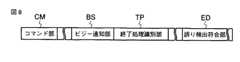
また、ホスト機器2による、カード1の終了処理サポート、非サポートの確認は、初期化コマンドによって行うこともできる。図8は、第1実施形態に係る初期化コマンドの内容の一部を示している。図8に示すように、初期化コマンドは、コマンド部CM、終了処理識別部TP、ビジー通知部BS、例えばCRC(Cyclic Redundancy Check)等の誤り検出符合などを用いた誤り検出符号部ED等を含んでいる。コマンド部CMには、このコマンドを識別するためのインデックスが設けられる。 The
ホスト機器2は、終了処理識別部TPのビットをホスト機器2が本実施形態に係る終了処理をサポートする旨(例えば“1”)にセットされた、初期化コマンドをカード1に供給する。 The
カード1は、初期化コマンドを受信すると、レスポンスをホスト機器2に返送する。レスポンスのフォーマットは、コマンドと同じである。カード1が、終了処理をサポートしている場合、終了処理識別部TAにおいて終了処理をサポートする旨、すなわち、コマンド内の終了処理識別部TSと同じビットがされたレスポンスをホスト機器2に返送する。このレスポンスを受信することにより、ホスト機器2は、アクセス中のカード1との間で、終了処理を行うことができることを知得する。 When the
カード1が、終了確認コマンドを認識するが、終了処理をサポートしていない場合、終了処理識別部TPを、サポートしていない旨のビット(例えば“0”)にセットされたレスポンスを返送する。 When the
ステップS32において、ホスト機器2によるカード1が終了処理をサポートしているか否かの判断後、ホスト機器2は、カード1へのデータの書き込みおよびカード1からのデータの読み出し(ステップS33、S34)を、必要な回数、行う。 In step S32, after determining whether or not the
(終了処理)
ホスト機器2は、例えばホスト機器2の電源がオフとされたことを受けて、以下に述べる終了処理を行う。カード1が終了処理をサポートしていない場合、従来と同様の方法によって、ホスト機器2からカード1への電源供給が停止されることにより、アクセスが終了する。(End processing)
For example, when the
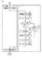
一方、カード1が終了処理をサポートしている場合、ホスト機器2およびカード1は、図9に示す終了処理を実行する。図9は、第1実施形態に係る終了処理時にホスト機器2およびカード1が取る工程を示すフローチャートである。図10は、終了処理のタイミングチャートを示している。 On the other hand, when the
図9、図10に示すように、ホスト機器2は、まず、コマンドラインCMD上で、機能停止コマンドをカード1に発行する(ステップS1)。機能停止コマンドは、カード1に終了処理を実行する旨の指示を含んでいる。機能停止コマンドは、上記のスイッチコマンドまたは新たに定義したコマンドを用いることができる。スイッチコマンドを用いた場合、図11に示すように、少なくとも、コマンド部CMと、セーブ指示部SSと、を有する。さらに、誤り検出符号部EDが設けられていてもよい。新たに定義したコマンドを用いる場合、コマンド部CM自体に機能停止コマンドという意味を持たせられるため、セーブ指示部SSは必ずしも必要ではない。セーブ指示部SSは、少なくとも、カード1が、システムデータを保存等をした後に、電源供給が停止されてもよい状態(電源停止待機状態)に移行すべき旨のビットパターン(例えば“1”)を取り得る。また、システムデータの保存無しに、カード1が電源停止待機状態に移行するビットパターン(例えば“0”)を有するようにすることもできる。 As shown in FIGS. 9 and 10, the
次に、カード1は、機能停止コマンドを受信する(ステップS2)。機能停止コマンドの受信を受けて、カード1は、コマンドラインCMD上でレスポンスを返信する。また、カード1は、ホスト機器2に対して、例えばデータラインDAT0上で、終了処理中によりビジーである旨の信号(例えば“0”)の送信を開始する(ステップS3)。 Next, the
次に、カード1への電源供給後のカード1の状態の変化が判定される(ステップS4)。カード1の状態の変化として、例えば、データが書き込まれた場合、カード1のロック/アンロック(Lock/Unlock)機能を切り替えた場合、プログラム可能なCSDレジスタの設定が変更された場合などが含まれる。 Next, a change in the state of the
カード1の状態に変化があった場合、カード1は、終了処理を実行する(ステップS5)。終了処理として、種々のものがあり得る。例えば、RAM25により記憶されていたシステムデータを、NAND型フラッシュメモリ11に保存することが挙げられる。システムデータを保存する場所は、例えば管理データ領域31とすることができる。または、NAND型フラッシュメモリ11以外に別途設けられた不揮発性メモリ内とすることもできる。なお、保存されるシステムデータは、システムデータ全てであってもよいし、その一部のみであってもよい。 When there is a change in the state of the
ここで、システムデータの例として、アドレス変換テーブルやアサインテーブルなどが挙げられる。アドレス変換テーブルとは、論理アドレスとNAND型フラッシュメモリ11の物理アドレスとを変換するためのテーブルである。また、アサインテーブルとは、データの格納に使用されているブロック(論理ブロックが割り当てられているブロック)と、データの格納に使用されていないブロック(論理ブロックが割り当てられていないブロック)とを識別するためのテーブルである。 Here, examples of the system data include an address conversion table and an assignment table. The address conversion table is a table for converting a logical address and a physical address of the
また、終了処理として、以下に述べる工程を実現することもできる。機能停止コマンドが定義されていない場合、カード1は、ホスト機器2からの電源供給がいつ終了するかを知得することができない。このため、電源供給が突然停止される可能性に備えるために、カードは、ホスト機器が書き込みを要求するデータを、逐次、NAND型フラッシュメモリに書き込むことが要求される。 Moreover, the process described below can also be realized as the termination process. If the function stop command is not defined, the
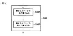
一方、機能停止コマンドが設けられることによって、カード1は、ホスト機器2からの電源供給が終了する前に、そのことを知得できる。そこで、図12に示すように、ステップS33の書き込みを、ホスト機器2がデータの書き込みを要求した際、書き込みデータの一部のみをNAND型フラッシュメモリ11に書き込み(ステップS33A)、残りを、後の、ホスト機器2からのアクセスが無いタイミング等を利用した書き込み(ステップS33B)、とすることができる。この場合、書き込みコマンドの供給とともに書き込まれない残りのデータは、例えばRAM25、またはNAND型フラッシュメモリ11のキャッシュ領域(仮書き込み領域)に保存しておくことができる。図12に示した書き込み方法を取ることにより、1つの書き込みコマンドによってカード1が実行する書き込みに要する時間を、書き込みデータの全体を書き込む場合より短くすることができる。 On the other hand, by providing the function stop command, the
この場合、未書き込みデータは、カード1への電源供給の終了前に完了している必要がある。このため、終了処理の1つとして、カード1は、未書き込みデータを、NAND型フラッシュメモリ11に書き込む。 In this case, the unwritten data needs to be completed before the power supply to the
なお、書き込みデータを全て書き込むか、2回以上に分けて書き込むかは、ホスト機器2が、カード1が終了処理をサポートしていることを知得した後に、書き込みコマンド内で指示しても良いし、カード1の方で判断しても良い。 Whether to write all of the write data or to write in two or more times may be instructed in the write command after the
次に、図9において、カード1は、正常に終了処理が行われたことを示すビットパターン(例えば“1”)をカード1内でセットする(ステップS6)。このビットパターン(フラグ)の形成領域(正常終了フラグ35)は、図3に示すように、NAND型フラッシュメモリ11内に設けられ、例えば管理データ領域31内に確保することができる。 Next, in FIG. 9, the
次に、カード1は、終了処理が完了したことを受けて、ホスト機器2に、ビジー状態が解除された旨の信号(例えば“1”)を送信する(ステップS7)。これにより、ホスト機器2は、カード1のビジー状態の解除を知得する。 Next, in response to the completion of the termination process, the
また、カード1は、ビジー状態の解除に伴い、ローパワーモードに移行する(ステップS8)。ローパワーモードは、カード1での電力消費が通常の状態より抑制され、初期化処理へと移行するのに必要な部位以外への電源供給が遮断される。これにより、カード1のローパワーモードへの正常な移行が完了する。 Further, the
ローパワーモードは、例えば以下の2つの方法のように、クロック信号の供給を制限することにより実現できる。1つ目は、カード1内のクロック回路がPLL(phese-locked loop)回路と発振器を含んでおり、発振器を停止させる場合である。この場合、発振器による電力消費を抑制するとともに、例えば、PLL回路が周波数の初期値を記憶しておくことにより電源供給開始後に短時間でクロック回路の発振周波数を安定させることができる。 The low power mode can be realized by limiting the supply of the clock signal, for example, as in the following two methods. In the first case, the clock circuit in the
2つ目は、ホスト機器2が供給するクロックを停止する場合である。カード1の動作中は、カード1内のフロントエンドにある大多数のフリップフロップにホスト機器2からクロック信号が供給される。例えばコマンドデコード回路内以外のフリップフロップに、このクロック信号が供給されることを停止することにより、カード1の消費電力を抑制できる。 The second case is when the clock supplied by the
カード1は、電源停止待機状態(不活性状態)に移行すると、再度初期化が開始されるまで、リード/ライトコマンドを含むあらゆるコマンドを受け付けない。こうすることによって、1度保存されたシステムデータが、カード1への電源供給停止の前に、変更されることが回避される。 When the
ホスト機器2は、ビジー状態が解除されたことに応じて、カード1への電源供給を停止する(ステップS9)。なお、カード1は、上記のように、ビジー状態の解除の後、ローパワーモードに移行する。こうすることにより、以下の利点を得られる。すなわち、通常、ビジー状態の解除の後、直ぐにカード1への電源供給が停止される。しかしながら、何等かの理由でホスト機器2からの電源供給が遮断されない場合が有り得る。このような場合に、カード1に無駄な電位が供給されることを回避することにより、ホスト機器2の電力消費を抑えることができる。 The
ホスト機器2において、カード1のビジー状態に対するタイムアウト時間が設定されていてもよい。例えば、カード1のビジー状態の開始時点から、ビジー状態が解除される前に設定されたタイムアウト時間が経過した場合、ホスト機器2はカード1への電源供給を停止する。この場合、カード1では終了処理が完了していないので、正常終了フラグ35は、その旨を示すビットパターン(例えば“0”)にセットされる。 In the
カード1の電源を入れた後、何も書き込まれなかった場合は、カード1の状態は何も変わっておらず、さらに前回、終了処理が完了している場合は、特に終了処理を行う必要はない。このため、ステップS10の判断の結果、正常終了フラグ35がセットされている場合、ステップS7に移行する。 If nothing is written after the
(初期化処理)
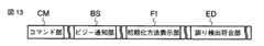
次に、初期化コマンドとレスポンスについて図13を参照して説明する。図13は、初期化コマンドとレスポンスのフォーマットは、同じものが用いられる場合を示している。図13に示すように、初期化コマンドは、少なくとも、コマンド部CMと、ビジー通知部BSを有する。コマンドには、初期化方法表示部FIは不要である。さらに、誤り検出符号部EDが設けられていても良い。(Initialization process)
Next, an initialization command and a response will be described with reference to FIG. FIG. 13 shows a case where the same format is used for the initialization command and the response. As shown in FIG. 13, the initialization command has at least a command part CM and a busy notification part BS. The command does not require the initialization method display unit FI. Further, an error detection code unit ED may be provided.
レスポンスにおいて、初期化方法表示部FIは必ずしも必須ではないが、この機能がある場合、初期化方法表示部FIには、カード1が、いずれの初期化方法で初期化を行ったかが示される。ビジー通知部BSは、カード1が初期化中である旨を示すビットパターン(例えば“1”)、初期化完了の旨を示すビットパターン(例えば“0”)が形成される。なお、レスポンス中の初期化方法表示部FIは、ビジー状態が解除されるまでに有効な値を示す。 In the response, the initialization method display unit FI is not necessarily indispensable, but when this function is provided, the initialization method display unit FI indicates which initialization method the
次に、カード初期化時にカードが取る工程について図14を参照して説明する。図14
は、第1実施形態に係るカード1が初期化時に取る工程を示すフローチャートである。図14に示すように、カード1は、初期化コマンドを受信する(ステップS21)と、初期化コマンドのレスポンスを返信する。レスポンス内のビジー通知部BSは、ビジー中である旨のビットパターンを有している(ステップS22)。この後も、ホスト機器2は、ビジーの解除によって初期化処理の終了をカード1から通知されるまで、初期化コマンドを発行し続ける。カード1は、最初の初期化コマンドを受信したことに応じて以下に述べる初期化処理を開始し、2回目以降の初期化コマンドに対しては、ビジー通知部BSにおいてビジー中である旨のビットパターンを有するレスポンスを単に返信し続ける。Next, the steps taken by the card at the time of card initialization will be described with reference to FIG. FIG.
These are the flowcharts which show the process which the card |
ステップS23において、カード1は、自身が保存している正常処理フラグ35を検査する。前回の終了処理が異常終了であった場合、正常処理フラグはクリアされているので、カード1は完全初期化を行う。すなわち、処理はステップS24に移行する。また、終了処理が正常終了であった場合、正常処理フラグはセットされているので、カード1は高速初期化を行う。すなわち、処理はステップS27に移行する。 In step S23, the
ステップS24の完全初期化は、従来の通常の初期化方法であり、以下に述べるように、メモリデータのエラーチェック、システムデータの保存等を含む。 The complete initialization in step S24 is a conventional normal initialization method, and includes error checking of memory data, storage of system data, and the like, as described below.
完全初期化処理において、カード1は、NAND型フラッシュメモリ11が記憶しているメモリデータにエラーが無いかをチェックする。例えば、前回のカード1への電源供給の停止が、メモリデータの書き込み中に行われた場合等にメモリデータが破損する。このようにしてメモリデータが破損している場合、メモリデータの修復が行われる。なお、このエラーチェック処理やエラー修復処理は、カード1内のNAND型フラッシュメモリ11の全ての領域に対して行うため、長時間を要する可能性がある。特に、メモリ容量の増大に応じて、より長期化する。 In the complete initialization process, the
次に、カード1は、システムデータを作成し、次いで、これをRAM25上に保存する(ステップS25)。 Next, the
ステップS27の高速初期化は、完全初期化から、幾つかの処理が省略されたり、完全初期化と異なる処理によって、完全初期化より短い時間で行われる初期化処理である。高速初期化の一例として、ステップS27において、カード1は、前回の終了処理の際にNAND型フラッシュメモリ11に保存しておいたシステムデータをRAM25上に読み出す。保存されているシステムデータが、システムデータ全体のうちの一部であった場合、これがRAM25上に保存されるとともに、残りの部分が再度作成される。以降、このシステムデータが利用される。また、高速初期化では、完全初期化の際に行われる、メモリデータのエラーのチェックが省略される。 The high-speed initialization in step S27 is an initialization process that is performed in a shorter time than the complete initialization by omitting some processes from the complete initialization or by a process different from the complete initialization. As an example of high-speed initialization, in step S27, the
システムデータが読み出された後、MPU23は初期化方法表示部パターンレジスタ36にいずれの初期化方法で初期化を行ったかを示すビットパターンを設定する(ステップS29)。次いで、MPU23は、ビジー通知部バターンレジスタにおいてビジー解除を示すビットパターンを設定する(ステップS30)。 After the system data is read, the
これらのレジスタに設定されたビットパターンは、カード1が次の初期化コマンドを受信したとき、そのレスポンスの初期化方法表示部FIおよびビジー通知部BSによってホスト機器2に通知される。ホスト機器2がこのレスポンスを受信することにより初期化コマンドの発行を停止するとともに、初期化処理が終了する。 The bit patterns set in these registers are notified to the
本発明の第1実施形態によれば、カード1は、ホスト機器2からの電源供給の停止を予め知得し、これに備えて終了処理を行うことができる。また、終了処理が正常に行われていた場合、高速で初期化を行うことができ、初期化時間を短くすることができる。 According to the first embodiment of the present invention, the
このように、メモリ容量の増加に従って完全初期化方法の改良のみでは初期化時間を短縮することが困難だとしても、初期化時間を短縮することが可能となる。このため、カードコントローラ12の設計に対する要求が緩和される。 Thus, even if it is difficult to shorten the initialization time only by improving the complete initialization method as the memory capacity increases, the initialization time can be shortened. For this reason, the request | requirement with respect to the design of the
なお、本実施形態では、特に、ホスト機器2がデジタルカメラ、ムービーカメラなどの場合、カード1が挿入され続けている状態での初期化時間を短くすることにより、電源を入れた直後の撮影を可能にすることができる。このため、本実施形態は、実用上、非常に有効である。 In this embodiment, particularly when the
正常終了フラグ35は、NAND型フラッシュメモリ11への書き込みなど、カード1の状態が以前と変更があった時点でクリアされる。そうするとカード1の状態に変化がなければ、終了処理を省略することができる。初期化が完了した時点でクリアしても良いが、その場合カード1の状態に変化がなくても、機能停止コマンドが来ると必ず終了処理を行う必要がある。 The
(第2実施形態)
第1実施形態は、RAM25が揮発性のメモリの場合に対応する。第2実施形態では、RAM25として、不揮発性のMRAM(magnetic random access memory)またはFeRAM(ferroelectric random access memory)が用いられる。この場合、システムデータが保存されるメモリ、および正常終了フラグ35が確保される領域が第1実施形態と異なるとともに、幾つかの処理が第1実施形態のそれと異なる。以下、異なる部分について説明する。(Second Embodiment)
The first embodiment corresponds to the case where the
図15は、本発明の第2実施形態に係るカードのハード構成を示すブロック図である。図15において、第1実施形態のRAM25の替わりに、MRAM、FeRAM等の不揮発性のRAM41が設けられる。正常終了フラグ35は、RAM41内またはNAND型フラッシュメモリ11内のいずれかに設けられる(図では、便宜上、両方に図示)。 FIG. 15 is a block diagram showing a hardware configuration of a card according to the second embodiment of the present invention. In FIG. 15, a
本実施形態において、カード1の初期化の際に作成されたシステムデータの全ては、RAM41に保存される。MRAM、FeRAMは不揮発性であり、且つ高速動作が可能であるため、システムデータは、第1実施形態の場合と異なり、カード1の動作中にSRAM上に移動される必要はない。このため、カード1が機能停止コマンドを受信した際の処理(図9)において、ステップS4の処理は不要となる。また、カード1が初期化時に取る工程(図14)において、ステップS27の処理は不要となる。その他は、第1実施形態と同じである。 In the present embodiment, all of the system data created when the
本発明の第2実施形態によれば、第1実施形態と同じ効果を得られる。 According to the second embodiment of the present invention, the same effect as the first embodiment can be obtained.
(第3実施形態)
図16は、本発明の第3実施形態に係るカードのハード構成を示すブロック図である。図16に示すように、第1実施形態のRAM25に加えて、不揮発性RAM41が設けられる。正常終了フラグ35は、不揮発性RAM41内またはNAND型フラッシュメモリ11内のいずれかに設けられる(図では、便宜上、両方に図示)。(Third embodiment)
FIG. 16 is a block diagram showing a hardware configuration of a card according to the third embodiment of the present invention. As shown in FIG. 16, in addition to the
本実施形態において、カード1の初期化の際に作成されたシステムデータの一部は、不揮発性RAM41に保存される。また、システムデータの残りの部分は、NAND型フラッシュメモリ11に保存される。システムデータのうちのRAM41に保存される部分は、RAM41が不揮発性であり、且つ高速動作が可能であるため、RAM25に移動されずに、不揮発性RAM41上で動作する。一方、NAND型フラッシュメモリ11に保存される部分は、カード1の動作中はRAM25に移動され、カード1への電源供給の停止に合わせて、第1実施形態と同様にNAND型フラッシュメモリ11または不揮発性RAM41に移動される。しかし、そのデータが初期化時に他の情報から作成容易な場合は、セーブしないで捨ててしまうこともできる。 In the present embodiment, a part of the system data created when the
カード1が機能停止コマンドを受信した際の処理(図9)において、ステップS4の処理は、システムデータのRAM25上の部分がNAND型フラッシュメモリ11または不揮発性RAM41に保存される処理に対応する。また、カード1が初期化時に取る工程(図14)において、ステップS27の処理は、システムデータのNAND型フラッシュメモリ11上のシステムデータがそのまま、または加工された上でRAM25に読み出される処理に対応する。その他は、第1実施形態と同じである。 In the processing when the
本発明の第3実施形態によれば、第1実施形態と同じ効果を得られる。 According to the third embodiment of the present invention, the same effect as the first embodiment can be obtained.
その他、本発明の思想の範疇において、当業者であれば、各種の変更例及び修正例に想到し得るものであり、それら変更例及び修正例についても本発明の範囲に属するものと了解される。 In addition, in the category of the idea of the present invention, those skilled in the art can conceive of various changes and modifications, and it is understood that these changes and modifications also belong to the scope of the present invention. .
1…カード、2…ホスト機器、3…バスインタフェース、4…スロット、5…電位供給部、6…読み取り/書き込み制御部、7…コマンド制御部、8…カード検出部、11…NAND型フラッシュメモリ、12…カードコントローラ、13…信号ピン、21…ホストインタフェースモジュール、22…レジスタ部、23…MPU、24…ROM、25、41…RAM、26…フラッシュコントローラ、27…バッファ、31…管理データ領域、32…機密データ領域、33…保護データ領域、34…ユーザデータ領域。DESCRIPTION OF
Claims (10)
Translated fromJapaneseホスト機器からの電源供給の停止を受け付け可能な状態に移行する終了処理を前記カードがサポートするか否かを示す情報を返送することを命ずる確認コマンドを発行することを特徴とするホスト機器。A host device into which a card having a nonvolatile semiconductor memory is inserted,
A host device which issues a confirmation command for instructing to return information indicating whether or not the card supports termination processing for shifting to a state in which a stop of power supply from the host device can be accepted.
前記ホスト機器からの電源供給の停止を受け付け可能な状態に移行する終了処理をサポートし、
前記終了処理をサポートするか否かを示す情報を返送することを命ずる確認コマンドを受信した際に、前記終了処理をサポートする旨を示すレスポンスを返送する、
ことを特徴とするカード。A card having a non-volatile semiconductor memory and inserted into a host device,
Supports termination processing to shift to a state where it is possible to accept the stop of power supply from the host device,
When receiving a confirmation command instructing to return information indicating whether or not to support the termination process, a response indicating that the termination process is supported is returned;
A card characterized by that.
前記終了処理が完了しなかったことが前記不揮発性半導体メモリに示されている場合、第1初期化方法により初期化処理を実行し、
前記終了処理が完了したことが前記不揮発性半導体メモリに示されている場合、前記第1初期化方法より短い時間で完了する第2初期化方法により初期化処理を実行する、
ことを特徴とする請求項6に記載のカード。An initialization command that orders initialization is supplied,
If the nonvolatile semiconductor memory indicates that the termination process has not been completed, the initialization process is executed by the first initialization method,
When the nonvolatile semiconductor memory indicates that the termination process is completed, the initialization process is executed by the second initialization method that is completed in a shorter time than the first initialization method.
The card according to claim 6.
Priority Applications (17)
| Application Number | Priority Date | Filing Date | Title |
|---|---|---|---|
| JP2005367632AJP4817836B2 (en) | 2004-12-27 | 2005-12-21 | Card and host equipment |
| PCT/JP2005/024205WO2006070906A1 (en) | 2004-12-27 | 2005-12-26 | Card and host apparatus |
| CN200910261980XACN101706709B (en) | 2004-12-27 | 2005-12-26 | Card and host apparatus |
| KR1020067016034AKR100871184B1 (en) | 2004-12-27 | 2005-12-26 | Cards, storage devices, and memory system control methods |
| CN2009101634785ACN101655775B (en) | 2004-12-27 | 2005-12-26 | Card and host apparatus |
| TW94146716ATWI305325B (en) | 2004-12-27 | 2005-12-27 | Card and host apparatus |
| US11/494,475US8423679B2 (en) | 2004-12-27 | 2006-07-28 | Card and host apparatus |
| US13/792,795US8533367B2 (en) | 2004-12-27 | 2013-03-11 | Card and host apparatus |
| US13/963,583US8671227B2 (en) | 2004-12-27 | 2013-08-09 | Card and host apparatus |
| US14/168,671US8812745B2 (en) | 2004-12-27 | 2014-01-30 | Card and host apparatus |
| US14/316,265US9128635B2 (en) | 2004-12-27 | 2014-06-26 | Card and host apparatus |
| US14/812,830US9857866B2 (en) | 2004-12-27 | 2015-07-29 | Card and host apparatus |
| US15/820,081US10466771B2 (en) | 2004-12-27 | 2017-11-21 | Card and host apparatus |
| US16/564,441US10747299B2 (en) | 2004-12-27 | 2019-09-09 | Card and host apparatus |
| US16/917,043US11169594B2 (en) | 2004-12-27 | 2020-06-30 | Card and host apparatus |
| US17/496,227US11789521B2 (en) | 2004-12-27 | 2021-10-07 | Card and host apparatus |
| US18/462,493US12287694B2 (en) | 2004-12-27 | 2023-09-07 | Card and host apparatus |
Applications Claiming Priority (3)
| Application Number | Priority Date | Filing Date | Title |
|---|---|---|---|
| JP2004378300 | 2004-12-27 | ||
| JP2004378300 | 2004-12-27 | ||
| JP2005367632AJP4817836B2 (en) | 2004-12-27 | 2005-12-21 | Card and host equipment |
Publications (2)
| Publication Number | Publication Date |
|---|---|
| JP2006209744Atrue JP2006209744A (en) | 2006-08-10 |
| JP4817836B2 JP4817836B2 (en) | 2011-11-16 |
Family
ID=36615013
Family Applications (1)
| Application Number | Title | Priority Date | Filing Date |
|---|---|---|---|
| JP2005367632AActiveJP4817836B2 (en) | 2004-12-27 | 2005-12-21 | Card and host equipment |
Country Status (6)
| Country | Link |
|---|---|
| US (11) | US8423679B2 (en) |
| JP (1) | JP4817836B2 (en) |
| KR (1) | KR100871184B1 (en) |
| CN (2) | CN101655775B (en) |
| TW (1) | TWI305325B (en) |
| WO (1) | WO2006070906A1 (en) |
Cited By (8)
| Publication number | Priority date | Publication date | Assignee | Title |
|---|---|---|---|---|
| JP2007317170A (en)* | 2006-04-28 | 2007-12-06 | Renesas Technology Corp | Ic module and cellular phone |
| JP2008217636A (en)* | 2007-03-07 | 2008-09-18 | Alpine Electronics Inc | Data processing apparatus and program starting method |
| WO2015064349A1 (en)* | 2013-10-29 | 2015-05-07 | 日立オートモティブシステムズ株式会社 | Physical-quantity detection device |
| US9983794B2 (en) | 2012-10-30 | 2018-05-29 | Toshiba Memory Corporation | Memory device and host device |
| WO2021010142A1 (en) | 2019-07-12 | 2021-01-21 | パナソニックIpマネジメント株式会社 | Onboard storage system |
| WO2021010143A1 (en) | 2019-07-12 | 2021-01-21 | パナソニックIpマネジメント株式会社 | In-vehicle secure storage system |
| WO2021199716A1 (en) | 2020-03-30 | 2021-10-07 | キヤノン株式会社 | Communication device, control method, and program |
| US12400012B2 (en) | 2021-06-16 | 2025-08-26 | Canon Kabushiki Kaisha | Information management system, method of controlling the information management system, and storage medium storing program |
Families Citing this family (13)
| Publication number | Priority date | Publication date | Assignee | Title |
|---|---|---|---|---|
| JP4970078B2 (en)* | 2007-02-21 | 2012-07-04 | 株式会社東芝 | Nonvolatile memory system |
| JP2008204582A (en)* | 2007-02-22 | 2008-09-04 | Elpida Memory Inc | Nonvolatile ram |
| US7668977B2 (en) | 2007-09-12 | 2010-02-23 | Infineon Technologies Austria Ag | Method for exchanging information between devices connected via a communication link |
| EP2513743B1 (en) | 2009-12-17 | 2017-11-15 | Toshiba Memory Corporation | Semiconductor system, semiconductor device, and electronic device initializing method |
| US9674310B2 (en)* | 2013-08-19 | 2017-06-06 | Qualcomm Incorporated | Operating M-PHY based communications over mass storage-based interfaces, and related connectors, systems and methods |
| CN103701707B (en)* | 2013-12-03 | 2017-02-15 | 杭州华三通信技术有限公司 | Network equipment |
| US9600179B2 (en)* | 2014-07-30 | 2017-03-21 | Arm Limited | Access suppression in a memory device |
| KR20160111222A (en)* | 2015-03-16 | 2016-09-26 | 에스케이하이닉스 주식회사 | Memory system including semiconductor memory device and memory controller, and operating method thereof |
| CN105005502B (en)* | 2015-07-15 | 2018-07-17 | 上海斐讯数据通信技术有限公司 | A kind of method and system terminated by kernel using SD card process |
| CN105307440B (en)* | 2015-12-03 | 2018-10-19 | 北京京东方多媒体科技有限公司 | A kind of door body structure and display device of communication jacks |
| KR102430983B1 (en)* | 2017-09-22 | 2022-08-09 | 삼성전자주식회사 | Storage device and method of operating the same |
| US11599081B2 (en)* | 2018-11-13 | 2023-03-07 | Rockwell Automation Technologies, Inc. | Method and apparatus for proxy execution and computation with an industrial controller |
| JP7450143B2 (en)* | 2020-09-25 | 2024-03-15 | パナソニックIpマネジメント株式会社 | Slave device, host device |
Citations (3)
| Publication number | Priority date | Publication date | Assignee | Title |
|---|---|---|---|---|
| JPH06124596A (en)* | 1991-11-28 | 1994-05-06 | Hitachi Ltd | Storage device using flash memory |
| JP2002051056A (en)* | 2000-08-04 | 2002-02-15 | Sony Corp | Communication control method, communication system and communication unit |
| JP2002150230A (en)* | 2000-11-15 | 2002-05-24 | Minolta Co Ltd | Information apparatus |
Family Cites Families (36)
| Publication number | Priority date | Publication date | Assignee | Title |
|---|---|---|---|---|
| JPH06105271A (en)* | 1992-09-16 | 1994-04-15 | Asahi Optical Co Ltd | IC memory card camera system |
| US5440244A (en)* | 1993-02-10 | 1995-08-08 | Cirrus Logic, Inc. | Method and apparatus for controlling a mixed voltage interface in a multivoltage system |
| JP2972501B2 (en)* | 1993-09-20 | 1999-11-08 | 富士通株式会社 | I/O subsystem and exclusive control method therefor |
| JP3604466B2 (en)* | 1995-09-13 | 2004-12-22 | 株式会社ルネサステクノロジ | Flash disk card |
| JP3565967B2 (en)* | 1995-12-21 | 2004-09-15 | 富士通株式会社 | IC card reading / writing device and IC card system |
| US5963255A (en)* | 1996-04-16 | 1999-10-05 | Apple Computer, Inc. | System and method for managing utilization of a battery |
| JP3493096B2 (en)* | 1996-06-07 | 2004-02-03 | 株式会社東芝 | Semiconductor integrated circuit, IC card, and IC card system |
| JP3821536B2 (en)* | 1997-05-16 | 2006-09-13 | 沖電気工業株式会社 | Nonvolatile semiconductor disk device |
| US6901457B1 (en)* | 1998-11-04 | 2005-05-31 | Sandisk Corporation | Multiple mode communications system |
| US7836236B2 (en)* | 2004-02-12 | 2010-11-16 | Super Talent Electronics, Inc. | Extended secure-digital (SD) devices and hosts |
| JP2001186556A (en)* | 1999-12-27 | 2001-07-06 | Toshiba Corp | Mobile wireless terminal |
| JP4649009B2 (en)* | 2000-03-08 | 2011-03-09 | 株式会社東芝 | Information processing apparatus having a card interface, card-type electronic equipment that can be mounted on the apparatus, and operation mode setting method in the apparatus |
| US6820148B1 (en)* | 2000-08-17 | 2004-11-16 | Sandisk Corporation | Multiple removable non-volatile memory cards serially communicating with a host |
| JP2002175090A (en)* | 2000-12-07 | 2002-06-21 | Sony Corp | Device and method of reproduction |
| JP4499935B2 (en)* | 2001-02-07 | 2010-07-14 | オリンパス株式会社 | Electronic camera |
| US6456084B1 (en) | 2001-03-28 | 2002-09-24 | Chung-Shan Institute Of Science And Technology | Radiation test system |
| US7185145B2 (en)* | 2001-06-04 | 2007-02-27 | Renesas Technology Corp. | Memory card |
| WO2002102072A1 (en)* | 2001-06-06 | 2002-12-19 | Nikon Corporation | Electronic imaging apparatus and electronic imaging system |
| US7418344B2 (en)* | 2001-08-02 | 2008-08-26 | Sandisk Corporation | Removable computer with mass storage |
| JP3707410B2 (en)* | 2001-09-17 | 2005-10-19 | インターナショナル・ビジネス・マシーンズ・コーポレーション | Computer apparatus, expansion device management method, and computer program |
| US20030097510A1 (en)* | 2001-11-20 | 2003-05-22 | Francis Joseph | System-On-Chip architecture that utilizes FeRAM and re-configurable hardware |
| TW542378U (en)* | 2002-02-08 | 2003-07-11 | C One Technology Corp | Multi-functional electronic card capable of detecting a card insertion |
| US7194638B1 (en)* | 2002-09-27 | 2007-03-20 | Cypress Semiconductor Corporation | Device and method for managing power consumed by a USB device |
| JP2004192452A (en) | 2002-12-12 | 2004-07-08 | Matsushita Electric Ind Co Ltd | Memory card |
| JP4454947B2 (en)* | 2003-03-20 | 2010-04-21 | キヤノン株式会社 | Recording apparatus and method for controlling power supply in the apparatus |
| US7305535B2 (en)* | 2003-04-17 | 2007-12-04 | Sandisk Corporation | Memory cards including a standard security function |
| US7114015B2 (en)* | 2003-09-03 | 2006-09-26 | Seagate Technology Llc | Memory card having first modular component with host interface wherein the first modular is replaceable with a second modular component having second host interface |
| JP2005135099A (en)* | 2003-10-29 | 2005-05-26 | Canon Inc | Image input apparatus and control method |
| US7139864B2 (en)* | 2003-12-30 | 2006-11-21 | Sandisk Corporation | Non-volatile memory and method with block management system |
| US7173863B2 (en)* | 2004-03-08 | 2007-02-06 | Sandisk Corporation | Flash controller cache architecture |
| US7594135B2 (en)* | 2003-12-31 | 2009-09-22 | Sandisk Corporation | Flash memory system startup operation |
| US7159766B2 (en)* | 2004-01-20 | 2007-01-09 | Standard Microsystems Corporation | Peripheral device feature allowing processors to enter a low power state |
| JP4515793B2 (en)* | 2004-03-11 | 2010-08-04 | 株式会社東芝 | Memory card device and memory card control method |
| JP4508721B2 (en)* | 2004-05-12 | 2010-07-21 | キヤノン株式会社 | Mobile device and control method thereof |
| WO2006026645A2 (en)* | 2004-08-30 | 2006-03-09 | Silicon Storage Technology, Inc. | Systems and methods for providing nonvolatile memory management in wireless phones |
| WO2006057049A1 (en) | 2004-11-26 | 2006-06-01 | Kabushiki Kaisha Toshiba | Card and host device |
- 2005
- 2005-12-21JPJP2005367632Apatent/JP4817836B2/enactiveActive
- 2005-12-26CNCN2009101634785Apatent/CN101655775B/enactiveActive
- 2005-12-26WOPCT/JP2005/024205patent/WO2006070906A1/enactiveApplication Filing
- 2005-12-26CNCN200910261980XApatent/CN101706709B/enactiveActive
- 2005-12-26KRKR1020067016034Apatent/KR100871184B1/enactiveActive
- 2005-12-27TWTW94146716Apatent/TWI305325B/enactive
- 2006
- 2006-07-28USUS11/494,475patent/US8423679B2/enactiveActive
- 2013
- 2013-03-11USUS13/792,795patent/US8533367B2/enactiveActive
- 2013-08-09USUS13/963,583patent/US8671227B2/enactiveActive
- 2014
- 2014-01-30USUS14/168,671patent/US8812745B2/enactiveActive
- 2014-06-26USUS14/316,265patent/US9128635B2/enactiveActive
- 2015
- 2015-07-29USUS14/812,830patent/US9857866B2/enactiveActive
- 2017
- 2017-11-21USUS15/820,081patent/US10466771B2/enactiveActive
- 2019
- 2019-09-09USUS16/564,441patent/US10747299B2/enactiveActive
- 2020
- 2020-06-30USUS16/917,043patent/US11169594B2/enactiveActive
- 2021
- 2021-10-07USUS17/496,227patent/US11789521B2/enactiveActive
- 2023
- 2023-09-07USUS18/462,493patent/US12287694B2/enactiveActive
Patent Citations (3)
| Publication number | Priority date | Publication date | Assignee | Title |
|---|---|---|---|---|
| JPH06124596A (en)* | 1991-11-28 | 1994-05-06 | Hitachi Ltd | Storage device using flash memory |
| JP2002051056A (en)* | 2000-08-04 | 2002-02-15 | Sony Corp | Communication control method, communication system and communication unit |
| JP2002150230A (en)* | 2000-11-15 | 2002-05-24 | Minolta Co Ltd | Information apparatus |
Cited By (16)
| Publication number | Priority date | Publication date | Assignee | Title |
|---|---|---|---|---|
| JP2007317170A (en)* | 2006-04-28 | 2007-12-06 | Renesas Technology Corp | Ic module and cellular phone |
| JP2008217636A (en)* | 2007-03-07 | 2008-09-18 | Alpine Electronics Inc | Data processing apparatus and program starting method |
| US10976930B2 (en) | 2012-10-30 | 2021-04-13 | Toshiba Memory Corporation | Memory device and host device |
| US11573701B2 (en) | 2012-10-30 | 2023-02-07 | Kioxia Corporation | Memory device and host device |
| US9983794B2 (en) | 2012-10-30 | 2018-05-29 | Toshiba Memory Corporation | Memory device and host device |
| US10353586B2 (en) | 2012-10-30 | 2019-07-16 | Toshiba Memory Corporation | Memory device and host device |
| US12189947B2 (en) | 2012-10-30 | 2025-01-07 | Kioxia Corporation | Memory device and host device |
| JPWO2015064349A1 (en)* | 2013-10-29 | 2017-03-09 | 日立オートモティブシステムズ株式会社 | Physical quantity detection device |
| WO2015064349A1 (en)* | 2013-10-29 | 2015-05-07 | 日立オートモティブシステムズ株式会社 | Physical-quantity detection device |
| US11977501B2 (en) | 2019-07-12 | 2024-05-07 | Panasonic Intellectual Property Management Co., Ltd. | On-board storage system for shortening time required for initializing storage device |
| WO2021010143A1 (en) | 2019-07-12 | 2021-01-21 | パナソニックIpマネジメント株式会社 | In-vehicle secure storage system |
| US11983304B2 (en) | 2019-07-12 | 2024-05-14 | Panasonic Intellectual Property Management Co., Ltd. | On-board secure storage system for detecting unauthorized access or failure and performing predetermined processing |
| WO2021010142A1 (en) | 2019-07-12 | 2021-01-21 | パナソニックIpマネジメント株式会社 | Onboard storage system |
| WO2021199716A1 (en) | 2020-03-30 | 2021-10-07 | キヤノン株式会社 | Communication device, control method, and program |
| US11789881B2 (en) | 2020-03-30 | 2023-10-17 | Canon Kabushiki Kaisha | Communication apparatus, control method, and storage medium |
| US12400012B2 (en) | 2021-06-16 | 2025-08-26 | Canon Kabushiki Kaisha | Information management system, method of controlling the information management system, and storage medium storing program |
Also Published As
| Publication number | Publication date |
|---|---|
| US20130332675A1 (en) | 2013-12-12 |
| US20200333874A1 (en) | 2020-10-22 |
| US20150331479A1 (en) | 2015-11-19 |
| US20220026980A1 (en) | 2022-01-27 |
| CN101655775B (en) | 2012-11-07 |
| CN101706709B (en) | 2012-12-05 |
| US8812745B2 (en) | 2014-08-19 |
| WO2006070906A1 (en) | 2006-07-06 |
| US20130191583A1 (en) | 2013-07-25 |
| TWI305325B (en) | 2009-01-11 |
| US8423679B2 (en) | 2013-04-16 |
| KR20060126764A (en) | 2006-12-08 |
| US11169594B2 (en) | 2021-11-09 |
| TW200641688A (en) | 2006-12-01 |
| CN101706709A (en) | 2010-05-12 |
| US20180095523A1 (en) | 2018-04-05 |
| US9857866B2 (en) | 2018-01-02 |
| US20060282550A1 (en) | 2006-12-14 |
| JP4817836B2 (en) | 2011-11-16 |
| KR100871184B1 (en) | 2008-12-01 |
| US20200004318A1 (en) | 2020-01-02 |
| US12287694B2 (en) | 2025-04-29 |
| US20140310460A1 (en) | 2014-10-16 |
| CN101655775A (en) | 2010-02-24 |
| US9128635B2 (en) | 2015-09-08 |
| US10466771B2 (en) | 2019-11-05 |
| US8533367B2 (en) | 2013-09-10 |
| US10747299B2 (en) | 2020-08-18 |
| US20140149667A1 (en) | 2014-05-29 |
| US11789521B2 (en) | 2023-10-17 |
| US8671227B2 (en) | 2014-03-11 |
| US20230418363A1 (en) | 2023-12-28 |
Similar Documents
| Publication | Publication Date | Title |
|---|---|---|
| US11789521B2 (en) | Card and host apparatus | |
| CN101471124B (en) | Memory card, card controller installed in memory card, and processing unit of memory card | |
| JP2006139556A (en) | Memory card and card controller | |
| JP4896450B2 (en) | Storage device | |
| JP2002109490A (en) | Memory card and clock control circuit | |
| JP4695385B2 (en) | Memory card and card controller | |
| US8812756B2 (en) | Method of dispatching and transmitting data streams, memory controller and storage apparatus | |
| US20080209092A1 (en) | Method and system for interfacing a plurality of memory devices using an mmc/sd protocol | |
| US20080162479A1 (en) | Memory card system and method for transmitting background information thereof | |
| CN117992082A (en) | Data storage device and firmware updating method | |
| JP2006236200A (en) | Card-like storage device and its host device | |
| JP2008123450A (en) | Electronic device capable of recording medium and memory access | |
| CN1918580A (en) | Cards and Host Devices | |
| CN117992081A (en) | Data storage device and firmware updating method | |
| JP2005202753A (en) | Semiconductor integrated circuit |
Legal Events
| Date | Code | Title | Description |
|---|---|---|---|
| A621 | Written request for application examination | Free format text:JAPANESE INTERMEDIATE CODE: A621 Effective date:20080728 | |
| A131 | Notification of reasons for refusal | Free format text:JAPANESE INTERMEDIATE CODE: A131 Effective date:20110510 | |
| A521 | Request for written amendment filed | Free format text:JAPANESE INTERMEDIATE CODE: A523 Effective date:20110629 | |
| TRDD | Decision of grant or rejection written | ||
| A01 | Written decision to grant a patent or to grant a registration (utility model) | Free format text:JAPANESE INTERMEDIATE CODE: A01 Effective date:20110802 | |
| A01 | Written decision to grant a patent or to grant a registration (utility model) | Free format text:JAPANESE INTERMEDIATE CODE: A01 | |
| A61 | First payment of annual fees (during grant procedure) | Free format text:JAPANESE INTERMEDIATE CODE: A61 Effective date:20110830 | |
| FPAY | Renewal fee payment (event date is renewal date of database) | Free format text:PAYMENT UNTIL: 20140909 Year of fee payment:3 | |
| R151 | Written notification of patent or utility model registration | Ref document number:4817836 Country of ref document:JP Free format text:JAPANESE INTERMEDIATE CODE: R151 | |
| FPAY | Renewal fee payment (event date is renewal date of database) | Free format text:PAYMENT UNTIL: 20140909 Year of fee payment:3 | |
| S111 | Request for change of ownership or part of ownership | Free format text:JAPANESE INTERMEDIATE CODE: R313111 | |
| R350 | Written notification of registration of transfer | Free format text:JAPANESE INTERMEDIATE CODE: R350 | |
| S111 | Request for change of ownership or part of ownership | Free format text:JAPANESE INTERMEDIATE CODE: R313111 | |
| R350 | Written notification of registration of transfer | Free format text:JAPANESE INTERMEDIATE CODE: R350 |