JP2006208790A - Illumination equipment - Google Patents
Illumination equipmentDownload PDFInfo
- Publication number
- JP2006208790A JP2006208790AJP2005021467AJP2005021467AJP2006208790AJP 2006208790 AJP2006208790 AJP 2006208790AJP 2005021467 AJP2005021467 AJP 2005021467AJP 2005021467 AJP2005021467 AJP 2005021467AJP 2006208790 AJP2006208790 AJP 2006208790A
- Authority
- JP
- Japan
- Prior art keywords
- wiring
- function control
- control element
- light emitting
- light
- Prior art date
- Legal status (The legal status is an assumption and is not a legal conclusion. Google has not performed a legal analysis and makes no representation as to the accuracy of the status listed.)
- Granted
Links
- 238000005286illuminationMethods0.000titleclaimsabstractdescription18
- 238000001514detection methodMethods0.000claimsabstractdescription107
- 230000005674electromagnetic inductionEffects0.000claimsabstractdescription15
- 238000005034decorationMethods0.000claimsdescription67
- 230000004397blinkingEffects0.000claimsdescription25
- 230000008033biological extinctionEffects0.000claimsdescription4
- 230000007423decreaseEffects0.000abstractdescription3
- 238000010586diagramMethods0.000description29
- 229910000859α-FeInorganic materials0.000description11
- 239000003990capacitorSubstances0.000description7
- 230000000694effectsEffects0.000description7
- 239000011347resinSubstances0.000description3
- 229920005989resinPolymers0.000description3
- RYGMFSIKBFXOCR-UHFFFAOYSA-NCopperChemical compound[Cu]RYGMFSIKBFXOCR-UHFFFAOYSA-N0.000description2
- 238000000034methodMethods0.000description2
- 230000010355oscillationEffects0.000description2
- 239000000758substrateSubstances0.000description2
- 206010034960PhotophobiaDiseases0.000description1
- 238000006243chemical reactionMethods0.000description1
- 239000011248coating agentSubstances0.000description1
- 238000000576coating methodMethods0.000description1
- 230000003247decreasing effectEffects0.000description1
- 230000007613environmental effectEffects0.000description1
- 238000009434installationMethods0.000description1
- 208000013469light sensitivityDiseases0.000description1
- 239000000696magnetic materialSubstances0.000description1
- 238000000465mouldingMethods0.000description1
- 230000000149penetrating effectEffects0.000description1
- 238000005476solderingMethods0.000description1
Images


Landscapes
- Non-Portable Lighting Devices Or Systems Thereof (AREA)
- Circuit Arrangement For Electric Light Sources In General (AREA)
- Illuminated Signs And Luminous Advertising (AREA)
Abstract
Translated fromJapaneseDescription
Translated fromJapanese本発明は、給電制御部から配線を介して給電することにより発光部を発光させる電飾装置において、前記配線部の任意の位置に該発光部の発光機能を制御する機能制御素子を着脱自在に取り付け、消灯・減光・点滅・環境の明暗による点灯及び消灯といった多彩な発光制御を発光部側からの素子の取付け操作で自由かつ簡単に行えるようにしたものである。 The present invention relates to an electrical decoration device that emits light from a light-emitting unit by supplying power from a power-supply control unit via a wiring, and a function control element that controls a light-emitting function of the light-emitting unit is detachable at an arbitrary position of the wiring unit. Various light emission controls such as mounting, turning off, dimming, blinking, lighting and turning off due to environmental light and darkness can be performed freely and easily by the element mounting operation from the light emitting section side.
電飾装置の発光素子へ電力を供給する手段としては、下記特許文献1に示す接続部のようにコネクター・ソケット・半田付け等の機械的接続構造を介して供給するものが一般的であるが、この機械的接続構造の電気的・機械的信頼性を確保するためには、これを設けられるだけの十分な空間が必要であり、これが発光部を大きくし、電飾装置を全体としても大型化してしまう原因となっていた。 As a means for supplying electric power to the light emitting element of the decoration device, one that supplies power through a mechanical connection structure such as a connector, a socket, and soldering as in the connection part shown in
このような課題を解決する一方法として、下記特許文献2に示すように、電磁誘導を用いて非接触にて発光素子に電力を供給する電飾装置が提案されている。 As a method for solving such a problem, as shown in
しかしながら、特許文献2に記載された従来の電磁誘導式の電飾装置においては、電飾装置の動作の切り替えは電磁誘導を使用した効果を生かすため、給電系にて行う必要があり、スイッチの設置場所は電源の近く置く必要があり、電飾装置の自由度を下げる要因となっていた。
また、従来の電磁誘導を利用しない電飾装置においても、特許文献1に記載された電飾装置のように、発光部とこの動作を変化させる選択部を、発光部とは離れて設置される制御部本体に設けることが多い。このため発光部の発光動作を切り替える操作を、制御部から離れた発光部側で行うことは困難であった。However, in the conventional electromagnetic induction type electric decoration device described in
Moreover, also in the conventional illumination device which does not use electromagnetic induction, like the illumination device described in
そこで本発明は、給電制御部からの配線を介した給電で発光部を発光させる電飾装置において、消灯・減光・点滅・環境の明暗による点灯及び消灯といった多彩な発光制御を発光部側からの簡単な操作で自由かつ簡単に行えるようにすることを目的とする。 Therefore, the present invention provides various lighting controls such as turning off, dimming, blinking, lighting in and out of the environment and turning off from the light emitting unit side, in an illumination device that emits light from the power supply through the wiring from the power supply control unit. It is intended to be able to perform freely and easily by simple operation.
請求項1に記載された電飾装置によれば、給電制御部に接続された配線に発光部を設け、前記給電制御部から前記配線を介して前記発光部に給電することにより前記発光部を発光させる電飾装置において、
前記配線の任意の位置に着脱可能なコイルを有する機能制御素子と、
前記機能制御素子が前記配線に設けられたことを検知して前記給電制御部による前記配線への給電パターンを変更させる機能制御手段とを備えることを特徴としている。According to the electrical decoration device described in
A function control element having a coil removable at an arbitrary position of the wiring;
And a function control unit that detects that the function control element is provided on the wiring and changes a power feeding pattern to the wiring by the power feeding control unit.
請求項2に記載された電飾装置は、請求項1記載の電飾装置において、
前記給電制御部は前記配線を交流駆動し、前記発光部は前記配線を挟むように設けられて前記配線と電磁誘導にて結合されるように構成されており、
前記機能制御素子の前記コイルは、前記配線の任意の位置に着脱可能な磁性体に巻装されており、
前記機能制御手段は、前記機能制御素子が前記配線に設けられたことによる前記配線の電流の変化を電圧の変化として検出する電流検出回路と、所定の周期で前記配線に信号を与えて前記発光部を駆動するとともに、この時に前記配線に生じた電圧の前記電流検出回路による検出結果に基づいて前記配線への給電パターンを変更させる制御回路とを備えることを特徴としている。The electrical decoration device described in
The power supply control unit is configured to AC drive the wiring, and the light emitting unit is provided so as to sandwich the wiring and is coupled to the wiring by electromagnetic induction.
The coil of the function control element is wound around a magnetic body that is detachable at an arbitrary position of the wiring,
The function control means includes a current detection circuit that detects a change in the current of the wiring as a change in voltage due to the function control element being provided in the wiring, and gives a signal to the wiring at a predetermined cycle to emit the light And a control circuit that changes a power feeding pattern to the wiring based on a detection result of the voltage generated in the wiring at this time by the current detection circuit.
請求項3に記載された電飾装置は、請求項1記載の電飾装置において、
前記給電制御部は前記配線を直流駆動し前記発光部は前記配線によって直列に接続されており、
前記機能制御素子の前記コイルは、前記配線の任意の位置に着脱可能な磁性体に巻装されており、
前記機能制御手段は、前記機能制御素子が前記配線に設けられたことによる前記配線の電流の変化を電圧の変化として検出する電流検出回路と、所定の周期で前記配線に高周波信号を与えて前記発光部を駆動するとともに、この時に前記配線に生じた電圧の前記電流検出回路による検出結果に基づいて前記配線への給電パターンを変更させる制御回路とを備えることを特徴としている。The electrical decoration device described in
The power supply control unit drives the wiring in direct current, and the light emitting unit is connected in series by the wiring,
The coil of the function control element is wound around a magnetic body that is detachable at an arbitrary position of the wiring,
The function control means includes a current detection circuit that detects a change in the current of the wiring as a change in voltage due to the function control element being provided in the wiring, and a high-frequency signal is given to the wiring at a predetermined cycle to And a control circuit that drives the light emitting unit and changes a power supply pattern to the wiring based on a detection result of the voltage generated in the wiring at this time by the current detection circuit.
請求項4に記載された電飾装置は、請求項2又は3記載の電飾装置において、
前記機能制御素子は、前記配線に設けた場合に第1の基準値より小さい検出電圧が前記配線に生じるような容量に設定された消灯用機能制御素子であり、
前記消灯用機能制御素子が前記配線に設けられて前記電流検出回路が前記検出電圧を検出している場合には、前記制御回路が前記配線への給電を停止して前記発光部を消灯するように構成されたことを特徴としている。The electrical decoration device described in
The function control element is a function control element for extinction set to a capacity such that a detection voltage smaller than a first reference value is generated in the wiring when provided in the wiring,
When the light-off function control element is provided in the wiring and the current detection circuit detects the detection voltage, the control circuit stops power supply to the wiring and turns off the light emitting unit. It is characterized by being configured.
請求項5に記載された電飾装置は、請求項2又は3記載の電飾装置において、
前記機能制御素子は、前記配線に設けた場合に第1の基準値よりは大きく前記第1の基準値より大きい第2の基準値よりは小さい検出電圧が前記配線に生じるような容量に設定された減光用機能制御素子であり、
前記減光用機能制御素子が前記配線に設けられて前記電流検出回路が前記検出電圧を検出している場合には、前記制御回路が前記配線への給電を間欠的に行うことにより前記発光部の発光輝度を減じるように構成されたことを特徴としている。The electrical decoration device described in
The function control element is set to have a capacitance such that when provided in the wiring, a detection voltage that is larger than the first reference value and smaller than the second reference value that is larger than the first reference value is generated in the wiring. Dimming function control element,
When the dimming function control element is provided in the wiring and the current detection circuit detects the detection voltage, the control circuit intermittently supplies power to the wiring, thereby the light emitting unit. It is characterized by being configured to reduce the light emission luminance.
請求項6に記載された電飾装置は、請求項2又は3記載の電飾装置において、
前記機能制御素子は、前記配線に設けた場合に第1の基準値より大きい第1の検出電圧を前記配線に発生させる動作と第1の基準値より小さい第2の検出電流を前記配線に発生させる動作とを繰り返し行わせるような容量及び回路構成を備えた点滅用機能制御素子であり、
前記点滅用機能制御素子が前記配線に設けられ、前記第1の検出電圧を検出した場合には前記制御回路は前記配線への給電を継続し、前記第2の検出電圧を検出した場合には前記制御回路は前記配線への給電を停止させることにより、前記発光部を点滅動作させるように構成されたことを特徴としている。The electrical decoration device described in
When the function control element is provided in the wiring, the function control element generates an operation of generating a first detection voltage larger than a first reference value in the wiring and a second detection current smaller than the first reference value in the wiring. A function control element for blinking having a capacity and a circuit configuration to repeatedly perform the operation of
When the blinking function control element is provided in the wiring, and the first detection voltage is detected, the control circuit continues to supply power to the wiring, and when the second detection voltage is detected. The control circuit is configured to cause the light emitting unit to blink by stopping power supply to the wiring.
請求項7に記載された電飾装置は、請求項2又は3記載の電飾装置において、
前記機能制御素子は、前記配線に設けた場合に環境が相対的に暗いと基準値より大きい第1の検出電圧を前記配線に発生させ、環境が相対的に明るいと基準値より小さい第2の検出電圧を前記配線に発生させるような容量及び光感応素子を有する回路構成を備えた光感知用機能制御素子であり、
前記光感知用機能制御素子が前記配線に設けられ、前記第1の検出電圧を検出した場合には前記制御回路は前記配線への給電を継続し、前記第2の検出電圧を検出した場合には前記制御回路は前記配線への給電を停止させることにより、前記発光部の点灯又は非点灯が環境の明暗に対応して選択されるように構成されたことを特徴としている。The electrical decoration device described in
When the environment is relatively dark when the function control element is provided in the wiring, the function control element generates a first detection voltage higher than a reference value in the wiring. It is a function control element for light sensing provided with a circuit configuration having a capacitance and a light sensitive element that generates a detection voltage in the wiring,
When the light sensing function control element is provided in the wiring and detects the first detection voltage, the control circuit continues to supply power to the wiring and detects the second detection voltage. The control circuit is configured such that lighting or non-lighting of the light emitting unit is selected corresponding to the lightness or darkness of the environment by stopping power supply to the wiring.
請求項1に記載された電飾装置によれば、発光部が設けられている配線の任意の位置に機能制御素子を取り付けるだけの簡単な操作を行えば、該機能制御素子が配線に設けられたことを給電制御部が検知して配線への給電パターンを該機能制御素子の機能に応じて変更するので、給電制御部から離れた位置において発光部の発光状態を任意に変更することができる。 According to the electrical decoration device described in
請求項2に記載された電飾装置によれば、特に配線を交流駆動して発光部を電磁誘導で交流駆動して発光させる電飾装置において、請求項1記載の前記効果を実現することができる。 According to the electrical decoration device described in
請求項3に記載された電飾装置によれば、特に給電制御部に発光部が配線によって直列に接続されて直流駆動を行う電飾装置において、請求項1記載の前記効果を実現することができる。 According to the electrical decoration device described in
請求項4に記載された電飾装置によれば、請求項2又は3記載の電飾装置による効果において、特に機能制御素子を配線に設けた場合に配線への給電を停止して発光部を消灯するような制御を行うことができる。 According to the illumination device described in
請求項5に記載された電飾装置によれば、請求項2又は3記載の電飾装置による効果において、特に機能制御素子を配線に設けた場合に配線への給電を間欠的に行わせて発光部の発光輝度を減じるような制御を行うことができる。 According to the electrical decoration device described in
請求項6に記載された電飾装置によれば、請求項2又は3記載の電飾装置による効果において、特に機能制御素子を配線に設けた場合に発光部が点滅動作するような制御を行うことができる。 According to the electrical decoration device described in
請求項7に記載された電飾装置によれば、請求項2又は3記載の電飾装置による効果において、特に機能制御素子を配線に設けた場合に発光部の点灯、非点灯が環境の明暗に対応して自動的に選択されるような制御を行うことができる。 According to the electrical decoration device described in
以下、本発明を実施するために特許出願人が出願時点で最良と思う本発明の実施の形態を図1〜図18を参照して説明する。
図1〜図10は本発明の実施の形態において電磁誘導を利用した電飾装置の例を示すものである。図1は同電飾装置の給電部の回路構成図であり、図2は同電飾装置の発光部(受電部)の断面図であり、図3は同発光部の回路構成図であり、図4は同電飾装置において発光状態の制御に用いられる機能制御素子の第1例の正面図であり、図5は同電飾装置の第1の駆動波形図であり、図6は同電飾装置の第2の駆動波形図であり、図7は同電飾装置において発光状態の制御に用いられる機能制御素子の第2例を示す回路構成図であり、図8は第2例の機能制御素子を用いた場合の駆動波形図であり、図9は同電飾装置において発光状態の制御に用いられる機能制御素子の第3例を示す回路構成図であり、図10は第3例の機能制御素子を用いた場合の駆動波形図である。
図11〜図18は本発明の実施の形態において電磁誘導を利用しない電飾装置の例を示すものである。図11は同電飾装置の回路構成図であり、図12は同電飾装置において発光状態の制御に用いられる機能制御素子の第4例の正面図であり、図13は第4例の機能制御素子を用いた場合の駆動波形図の一例であり、図14は第4例の機能制御素子を用いた場合の駆動波形図の他の例であり、図15は同電飾装置において発光状態の制御に用いられる機能制御素子の第5例の回路構成図であり、図16は第5例の機能制御素子を用いた場合の駆動波形図の一例であり、図17は同電飾装置において発光状態の制御に用いられる機能制御素子の第6例の回路構成図であり、図18は第6例の機能制御素子を用いた場合の駆動波形図の一例である。DESCRIPTION OF THE PREFERRED EMBODIMENTS Hereinafter, embodiments of the present invention, which the patent applicant believes best at the time of filing to implement the present invention, will be described with reference to FIGS.
FIGS. 1-10 shows the example of the electrical decoration apparatus using electromagnetic induction in embodiment of this invention. 1 is a circuit configuration diagram of a power feeding unit of the electrical decoration device, FIG. 2 is a sectional view of a light emitting unit (power receiving unit) of the electrical decoration device, and FIG. 3 is a circuit configuration diagram of the light emitting unit. FIG. 4 is a front view of a first example of a function control element used for controlling the light emission state in the electric decoration device, FIG. 5 is a first drive waveform diagram of the electric decoration device, and FIG. FIG. 7 is a second drive waveform diagram of the decoration device, FIG. 7 is a circuit configuration diagram showing a second example of a function control element used for controlling the light emission state in the same decoration device, and FIG. 8 is a function of the second example. FIG. 9 is a drive waveform diagram in the case of using a control element, FIG. 9 is a circuit configuration diagram showing a third example of a function control element used for controlling a light emission state in the electrical decoration device, and FIG. 10 is a diagram of the third example. It is a drive waveform figure at the time of using a function control element.
FIGS. 11-18 shows the example of the electrical decoration apparatus which does not utilize electromagnetic induction in embodiment of this invention. FIG. 11 is a circuit configuration diagram of the electrical decoration device, FIG. 12 is a front view of a fourth example of a function control element used for controlling the light emission state in the electrical decoration device, and FIG. 13 is a function of the fourth example. FIG. 14 is an example of a drive waveform diagram when the control element is used, FIG. 14 is another example of the drive waveform diagram when the function control element of the fourth example is used, and FIG. 15 is a light emission state in the electrical decoration device. FIG. 16 is an example of a drive waveform diagram in the case where the function control element of the fifth example is used, and FIG. FIG. 18 is a circuit configuration diagram of a sixth example of the function control element used for controlling the light emission state, and FIG. 18 is an example of a drive waveform diagram when the function control element of the sixth example is used.
1.電磁誘導を利用した電飾装置(図1〜図10)
(1)電飾装置の構成等(図1〜図3)
本例の電飾装置は、給電駆動回路8に接続された給電コイル2を備えた給電部3と、発光素子4に接続された受電コイル5を備えた貫通円筒形の小型発光部材として構成された発光部(受電部とも呼ぶ)6を有し、前記給電部3の給電コイル2が前記発光部6を貫通するように配置して、前記給電コイル2と前記受電コイル5を電磁結合が成立する給電状態に置くことにより、電磁誘導で給電部3から発光部6に対し非接触で給電を行い発光素子4を発光させる装置である。1. An electrical decoration device using electromagnetic induction (FIGS. 1 to 10)
(1) Configuration of the illumination device (FIGS. 1 to 3)
The electrical decoration device of this example is configured as a small cylindrical light-emitting member having a cylindrical shape including a
図1に示すように、前記給電部3は、所望のパターンで配置された配線としての給電コイル2と、この給電コイル2に駆動信号を供給する給電駆動回路8を有している。
給電駆動回路8は、電源1(電源回路もしくは電池)と、駆動信号の基準となる信号を発生する発振器9(発振回路)と、必要に応じて発振器9からの信号をもとに駆動信号に変換する分周器10(分周回路)と、給電コイル2の駆動タイミングを制御する制御回路11と、制御回路11からの信号により給電コイル2を分周器10からの信号で数kHz〜数十kHzで交流駆動する駆動回路12とを有している。さらに、給電駆動回路8は、後述する機能制御素子が前記給電コイル2に設けられた場合に、給電コイル2に流れる電流の変化を電圧値の変化として検出し、その検出結果を制御回路11に与えて駆動回路12を制御させるための電流検出回路7を備えている。As shown in FIG. 1, the
The power
図2にて発光部6の全体構成を説明する。発光部6の磁性体14は貫通した筒状(本例では貫通円筒状)であり、その周囲に受電コイル5が巻かれている。受電コイル5に接続された前記発光素子4は、受電コイル5の表面に沿って設けられた基板20に抵抗21とともに設けられている。磁性体14、受電コイル5及び基板20(発光素子4及び抵抗21を含む)は、前記磁性体14の中心に前記給電コイル2が貫通するための貫通孔が形成されるよう、透光性を有する樹脂等の被覆体15によりモールド等の手法で覆われており、全体として貫通円筒形状をなす電飾のための一発光体を構成している。 The whole structure of the
図3にて発光部6の回路構成を説明する。発光部6は、磁性体14と、該磁性体14に巻き込まれた一つの受電コイル5と、受電コイル5の両端に接続されて該コイル5に誘起された電力にて駆動される発光素子4(例えばLED)とを有している。例えばLEDのような発光素子4は、導通方向が互いに逆になるように2個ずつ合計4個が一つの受電コイル5の両端に電流を規制するための抵抗21を介して接続されている。 The circuit configuration of the
本例の発光部6の発光素子4を発光させる場合には、給電部3の給電コイル2が発光部6の中心を貫通するように発光部6を給電コイル2に対して取り付ける。発光部6は、給電コイル2に沿って移動させることができるので、一旦定めた発光部6の配置は、後に必要に応じて変更することができる。この状態で給電コイル2を駆動すれば、受電コイル5に誘導電流を誘起してその発光素子4を発光させることができる。 When the
(2)消灯用及び減光用機能制御素子(図4〜図6)
前記電飾装置において、発光部6が取り付けられた給電コイル2に必要に応じて着脱自在に取り付けられ、給電コイル2からの給電を受けて発光している発光部6を消灯し、又は減光することができる機能制御素子について、図4〜図6を参照して説明する。(2) Function control element for turning off and dimming (FIGS. 4 to 6)
In the electrical decoration device, the
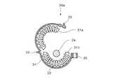
図4に示すように、この機能制御素子30は、発光部6と同様に貫通円筒形の部材であるが、必要に応じて給電コイル2の所望位置に着脱自在に取り付ける必要性から、その円筒形は縦に2分割されて開閉可能となっている。すなわち、この機能制御素子30は、円筒形の母線に沿って縦に2分割された貫通円筒形のフェライトコア31a,31b(磁性体)を有しており、この分割されたフェライトコア31a,31bには発光部6と同様に被覆銅線が巻き込まれた1つのコイル32が設けられている。そして、コイル32が巻き込まれたフェライトコアの一方31a及び他方31bは、貫通円筒体を縦に2分割した二つの部品をヒンジ33で連結して開閉可能とした樹脂製のホルダー34の各部品内にそれぞれ保持されている。ホルダー34の各部品を閉じてロック部35で固定すると、ホルダー34内の2つのフェライトコア31a,31bは分割部分で接触し、磁性体として実質的に一体の貫通円筒形となる。従って、使用者は、給電コイル2に設けた発光部6の動作を変更したいときには、給電コイル2の任意の位置に給電コイル2を挟み込むように該機能制御素子30を取り付けることができる。 As shown in FIG. 4, the
機能制御素子30は、フェライトコア31a,31bのサイズとコイル32の巻き数により容量が変化する。これを利用し、給電駆動回路8の電流検出回路7による給電コイル2の電圧検出レベルと、機能制御素子30の容量を組み合わせることにより、所望の発光状態を実現する制御機能を備えた機能制御素子30を製造することができる。
本例では、前述した基本構造を有する機能制御素子30において、容量を任意に設定することで、例えば消灯用機能制御素子と減光用機能制御素子を得ることができ、以下にこれらの作用について説明する。The capacity of the
In this example, in the
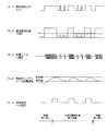
図5は、給電コイル2に発光部6が設けられた電飾装置において、消灯用機能制御素子を給電コイル2に設けて発光部6を消灯した状態から、次にこれを取外して発光部6を発光させ、その後再度装着して発光部6を消灯する動作を各部の信号の波形で示している。 FIG. 5 shows a lighting device in which the
まず、消灯用機能制御素子が給電コイル2に設けられている期間中、制御回路11は、信号(1-1) で示すように、消灯用機能制御素子を検出するために、所定の時間間隔で検知信号を与えて駆動回路12を動作させ、給電コイル2を駆動している。この期間、給電コイル2には信号(1-3) で示すように制御回路11の信号(1-1) に対応する間欠的な波形の信号が生じており、この給電コイル2に流れた電流は信号(1-2) に示すように電流検出回路7で電圧値として検出される。この電流検出回路7で検出された電圧値は、給電コイル2に消灯用機能制御素子が装着されているために、消灯用機能制御素子の容量の分に対応して低下しており、設定値R1以下となっている。制御回路11は、電流検出回路7で検出された電圧値が設定値R1以下である場合、消灯用機能制御素子が給電コイル2に装着されていると判断し、駆動回路12への出力を停止する。従って、消灯用機能制御素子が給電コイル2に設けられている期間中、発光素子6が点灯せずに消灯した状態が継続する。なお、制御回路11から出力される検出用の信号は間欠的であるので電力消費は少なく、またこの検出用の信号で発光部6が発光駆動されることはない。 First, during the period in which the extinguishing function control element is provided in the
制御回路11はこの様な消灯用機能制御素子の検出動作を繰り返す。そして、この検出動作時に、消灯用機能制御素子がが取り外されると、電流検出回路7が検出した電圧値は信号(1-2) で示すように設定値R2以上となり、この時制御回路11は消灯用機能制御素子が給電コイル2から取り外されたと判断し、駆動回路12への出力を連続して実行するので、発光部6は発光を始めるとともにその状態を継続することになる。 The
その後、消灯用機能制御素子を給電コイル2に再び装着すれば、前述したのと同様の動作で制御回路11は消灯用機能制御素子が給電コイル2に装着されていると判断し、駆動回路12への出力を停止し、発光部6は再び消灯する。 After that, if the extinguishing function control element is attached to the
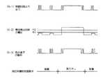
図6は、給電コイル2に発光部6が設けられた電飾装置において、消灯用機能制御素子を給電コイル2に設けて発光部6を消灯した状態から、次にこれを取外して発光部6を発光させ、その後減光用機能制御素子を装着して発光している発光部6の輝度を減少させ、その後消灯用機能制御素子を再び装着して発光部6を消灯する動作を各部の信号の波形で示している。 FIG. 6 shows an illumination device in which the
前述のように、消灯用機能制御素子を給電コイル2に設けて発光部6を消灯した状態から、消灯用機能制御素子が装着されていない発光状態に移ると、電流検出回路7は、設定値R2以上の電圧値を検出し、これに応じて制御回路11は連続的に信号を出力するようになり、給電コイル2は常時駆動されて発光部6は発光を継続する。 As described above, when the function control element for turning off is provided in the
ここで、給電コイル2に減光用機能制御素子が装着されると、信号(2-2) に示すように給電コイル2が駆動されているときの電圧値がR2以下R1以上のレベルとなり、制御回路11は係る給電コイル2の電圧レベルから給電コイル2に減光用機能制御素子が装着されたと判断し、信号(2-1) に示すように所定のタイミングで間欠的な出力を行い、これによって給電コイル2は信号(2-3) に示すように間欠駆動されて該給電コイル2に設置された発光部6も間欠的に発光することとなり、明るさが低下して減光動作となる。 Here, when the dimming function control element is attached to the
さらに給電コイル2に消灯用機能制御素子を装着すると、前述したように給電コイル2が駆動されているときの電圧値はR1以下のレベルとなり、制御回路11からの出力は停止し、給電コイル2への駆動が停止して発光部6は消灯し、前述した検出動作へ移行する。 Further, when the
(3)点滅用機能制御素子(図7、図8)
上記1.(2)では、機能制御素子は比較的単純なコイル32を主体として構成されていたが、本例の機能制御素子は特定の機能を備えた回路を組み込むことによりさらに点灯の制御態様を多様化して使用者の利便性及び使用上の自由度を向上させたものである。
すなわち、本例は、前記電飾装置において、発光部6が取り付けられた給電コイル2に必要に応じて着脱自在に取り付けられ、給電コイル2からの給電を受けて発光している発光部6を点滅動作させる点滅用機能制御素子に関するものである。(3) Function control element for blinking (FIGS. 7 and 8)
Above 1. In (2), the function control element is composed mainly of a relatively
That is, in this example, the
図7に示すように、本例の点滅用機能制御素子40は、分割円筒形構造で給電コイル2に着脱可能なフェライト(磁性体)にまかれた受電コイル5と、整流回路36と、点滅間隔を設定する時限用コンデンサー37及び抵抗38と、電圧比較回路39と、電圧比較回路39からの出力に応じてON/OFFすることにより装着時に給電コイル2から見た容量を変化させるスイッチング素子としてのトランジスタ45と、トランジスタ45の出力を与えられて本回路の容量を設定する負荷抵抗46とを有している。 As shown in FIG. 7, the blinking
図8は、給電コイル2に発光部6が設けられた電飾装置において、機能制御素子がない状態から、次に本例の点滅用機能制御素子40を給電コイル2に装着して発光部6を点滅させ、その後これを取り外して発光部6を連続点灯の状態に戻す動作を各部の信号の波形で示している。 FIG. 8 shows a lighting apparatus in which the
特に機能制御素子が設けられていない発光部6の連続発光状態において、点滅用機能制御素子40が給電コイル2に装着されると、信号(3-4) に示すように時限用コンデンサー37は充電を開始するが、電圧値が設定値1より低い間は電圧比較回路39の出力はLとなり、トランジスタ45がONとなって信号(3-5) に示すように負荷抵抗46に電流を流すため、信号(3-3) に示す給電コイル2に流れる電流は、電流検出回路7が検出する信号(3-2) のようにR1レベル以上の電圧値となる。かかる電流検出回路7の検出結果に応じて信号(3-1) に示すように制御回路11の出力は連続し、発光部6は点灯状態を維持する。 In particular, when the blinking
時限用コンデンサー37の充電が進み、電圧が上昇し、信号(3-4) に示すように設定値1を超えると、電圧比較回路39の出力はHとなり、トランジスタ45はOFFとなって信号(3-5) に示すように負荷抵抗46に電流が流れなくなるため、信号(3-3) に示す給電コイル2に流れる電流は、電流検出回路7が検出する信号(3-2) のようにR1レベル以下の電圧値となる。かかる電流検出回路7の検出結果に応じて信号(3-1) に示すように制御回路11の出力は停止し、発光部6は消灯し、前述した検出動作へ移行する。 When the time-
検出動作になると時限用コンデンサー37は放電状態となり、信号(3-4) に示すように電圧値は徐々に低下して行き、設定値2より低くなると電圧比較回路7の出力は再びLとなり、トランジスタ45がONとなって信号(3-5) に示すように再び負荷抵抗46に電流を流すため、前述したのと同様の作用で再び給電コイル2にはR1レベル以上の電圧値となる。このため制御回路11の出力は連続し、発光部6は点灯状態を維持する。
以上のような動作を繰り返すことにより発光部6は点滅動作となる。When the detection operation is started, the time-
By repeating the operation as described above, the
(4)光感知用機能制御素子(図9、図10)
本例は、前記1.(3)で説明した点滅用機能制御素子40と同様に、特定の機能を備えた回路を組み込むことによりさらに点灯の制御態様を多様化して使用者の利便性及び使用上の自由度を向上させたものである。
すなわち、本例は、回路構成中に光感応素子を有しており、前記電飾装置の発光部6が取り付けられた給電コイル2に取り付けた場合、環境が相対的に暗いと発光部6を点灯させ、環境が相対的に明るいと発光部6を消灯することができる光感知用機能制御素子に関するものである。(4) Light sensing function control element (FIGS. 9 and 10)
In this example, the 1. Like the blinking
That is, this example has a light sensitive element in the circuit configuration, and when the
図9に示すように、本例の光感知用機能制御素子50は、磁性体にまかれた受電コイル5と、整流回路42と、cds等の光感応素子43と、光感応素子43の出力に応じてON/OFFすることにより装着時に給電コイル2から見た容量を変化させるスイッチング素子としてのトランジスタ45と、トランジスタ45からの出力が与えられて本回路の容量を設定する負荷抵抗46とを有している。 As shown in FIG. 9, the light sensing
図10は、給電コイル2に発光部6を設けた電飾装置に本例の光感知用機能制御素子50を装着した場合において、夜間と昼間における発光部6の点灯・消灯動作を各部の信号の波形で示している。 FIG. 10 shows the signal of each part when the light-
給電コイル2に光感知用機能制御素子50が装着された状態では、光感知用機能制御素子50に外光が当たる昼間には光感応素子43の抵抗値が低くなり、信号(4-4) に示すようにトランジスタ45のベース電圧が設定値1より高くなってトランジスタ45はOFFとなり、信号(4-5) に示すように負荷抵抗46に電流が流れなくなるため、信号(4-3) に示す給電コイル2に流れる電流は、電流検出回路7が検出する信号(4-2) のようにR1レベル以下の電圧値となる。かかる電流検出回路7の検出結果に応じて信号(4-1) に示すように制御回路11の出力は停止し、発光部6は消灯し、前述した検出動作へ移行する。 In the state where the light sensing
夜間になり外光が無くなると光感応素子43の抵抗値が大きくなり、信号(4-4) に示すようにトランジスタ45のベース電圧が設定値1より低くなってトランジスタ45はONとなり、信号(4-5) に示すように負荷抵抗46に電流を流すため、信号(4-3) に示す給電コイル2に流れる電流は、電流検出回路7が検出する信号(4-2) のようにR1レベル以上の電圧値となる。かかる電流検出回路7の検出結果に応じて信号(4-1) に示すように制御回路11の出力は連続し、発光部6は点灯状態を維持する。 At night, when the outside light disappears, the resistance value of the
2.電磁誘導を利用しない電飾装置(図11〜図18)
(1)電飾装置の構成等(図11、図12)
図11に示すように、給電駆動回路8aには、発光部としての多数の発光素子4が配線2aを介して直列に接続されており、発光素子4が直列に設けられた該配線2aは本例では3系列とされている。2. An electrical decoration device that does not use electromagnetic induction (FIGS. 11 to 18)
(1) Configuration of the illumination device (FIGS. 11 and 12)
As shown in FIG. 11, in the power
前記給電駆動回路8aは、電源1a(電源回路もしくは電池)と、駆動信号の基準となる信号を発生する発振器9a(発振回路)と、必要に応じて発振器9aからの信号をもとに駆動信号に変換する分周器10a(分周回路)と、発光素子4の駆動を制御する制御回路11aと、制御回路11aからの信号により発光素子4を直流駆動する駆動回路12aとを有している。さらに、給電駆動回路8aは、後述する機能制御素子が前記配線2aに設けられた場合に、配線2aに流れる電流の変化を電圧値の変化として検出し、その検出結果を制御回路11aに与えて駆動回路12aを制御させるための電流検出回路7aを備えている。 The power
(2)消灯用及び減光用機能制御素子(図12〜図14)
前記電飾装置において、発光素子4が取り付けられた配線2aに必要に応じて着脱自在に取り付けられ、発光している発光素子4を消灯し、又は減光することができる機能制御素子について、図12〜図14を参照して説明する。(2) Function control element for turning off and dimming (FIGS. 12 to 14)
In the electrical decoration device, a function control element that can be detachably attached to the
図12に示すように、この機能制御素子30aは、貫通円筒形の部材であるが、必要に応じて配線2aの所望位置に着脱自在に取り付ける必要性から、その円筒形は縦に2分割されて開閉可能となっている。すなわち、この機能制御素子は、円筒形の母線に沿って縦に2分割された貫通円筒形のフェライトコア31a,31b(磁性体)を有しており、この分割されたフェライトコア31a,31bには被覆銅線が巻き込まれた1つのコイル32が設けられている。そして、コイル32が巻き込まれたフェライトコアの一方31a及び他方31bは、貫通円筒体を縦に2分割した二つの部品をヒンジ33で連結して開閉可能とした樹脂製のホルダー34の各部品内にそれぞれ保持されている。ホルダー34の各部品を閉じてロック部35で固定すると、ホルダー34内の2つのフェライトコア31a,31bは分割部分で接触し、磁性体として実質的に一体の貫通円筒形となる。従って、使用者は、配線2aに設けた発光素子4の動作を変更したいときには、配線2aの任意の位置に配線2aを挟み込むように該機能制御素子30aを取り付けることができる。
なお、本例では配線2aが3系列あるので、機能制御素子は各配線ごとに同一又は異なる機能のものを設けてもよいし、3系列まとめて1つの機能制御素子を設けてもよい。As shown in FIG. 12, the
In this example, since there are three series of
機能制御素子30aは、フェライトコア31a,31bのサイズとコイル32の巻き数により容量が変化する。これを利用し、給電制御回路8aの電流検出回路7aによる配線2aの電圧検出レベルと、機能制御素子30aの容量を組み合わせることにより、所望の発光状態を実現する制御機能を備えた機能制御素子を製造することができる。
本例では、前述した基本構造を有する機能制御素子30aにおいて、容量を任意に設定することで、例えば消灯用機能制御素子と減光用機能制御素子を得ることができ、以下にこれらの作用について説明する。The capacity of the
In this example, in the
図13は、配線2aに発光素子4が直列に設けられた電飾装置において、消灯用機能制御素子を配線2aに設けて発光素子4を消灯した状態から、次にこれを取外して発光素子4を発光させ、その後再度装着して発光素子4を消灯する動作を各部の信号の波形で示している。 FIG. 13 shows an illumination apparatus in which the
まず、消灯用機能制御素子が配線2aに設けられている期間中、制御回路11は、信号(5-1) で示すように、消灯用機能制御素子を検出するために、所定の時間間隔で高い周波数の検知信号を与えて駆動回路12を動作させ、配線2aを介して発光素子4を駆動している。この検知期間における検知信号の駆動周波数は例えば数百〜数十kHz程度であり、検知間隔は数十ms程度である。この期間、配線2aの発光素子4には信号(5-3) で示すように制御回路11の信号(5-1) に対応する波形の信号が生じており、この発光素子4及び配線2aに流れた電流は信号(5-2) に示すように電流検出回路7で電圧値として検出される。この電流検出回路7で検出された電圧値は、配線2aに消灯用機能制御素子が装着されているために、消灯用機能制御素子の容量の分に対応して低下しており、設定値R1以下となっている。制御回路11は、電流検出回路7で検出された電圧値が設定値R1以下である場合、消灯用機能制御素子が配線2aに装着されていると判断し、駆動回路12への出力を停止する。従って、消灯用機能制御素子が配線2aに設けられている期間中、発光素子4が点灯せずに消灯した状態が継続する。なお、制御回路11から出力される検出用の高周波信号は間欠的であるので電力消費は少なく、またこの検出用の信号で発光素子4が発光駆動されることはない。 First, during the period in which the extinction function control element is provided in the
制御回路11はこの様な消灯用機能制御素子の検出動作を繰り返す。そして、この検出動作時に、消灯用機能制御素子がが取り外されると、電流検出回路7が検出した電圧値は信号(5-2) で示すように設定値R2以上となり、この時制御回路11は消灯用機能制御素子が配線2aから取り外されたと判断し、駆動回路12への出力を連続して実行するので、発光部6は発光を始めるとともにその状態を継続することになる。 The
その後、消灯用機能制御素子を配線2aに再び装着すれば、前述したのと同様の動作で制御回路11は消灯用機能制御素子が配線2aに装着されていると判断し、駆動回路12への出力を停止し、発光素子4は再び消灯する。 After that, if the turn-off function control element is attached to the
図14は、配線2aに発光素子4が直列に設けられた電飾装置において、機能制御素子がなく発光素子4が連続発光している状態から、次に減光用機能制御素子を装着して発光している発光素子4の輝度を減少させ、その後減光用機能制御素子を取り外して再び発光素子4を連続点灯させ、その後消灯用機能制御素子を配線2aに設けて発光素子4を消灯する動作を各部の信号の波形で示している。 FIG. 14 shows an illumination device in which the
発光素子4への配線2aに機能制御素子が無いときには、信号(6-2) で示すように電流検出回路7の電圧値はR2のレベル以上となり、信号(6-1) で示すように制御回路11からは連続の出力が行われ、発光素子4は信号(6-3) で示すように常時点灯される。 When there is no function control element in the
次に、発光素子4への配線2aに減光用機能制御素子が装着されると、信号(6-2) で示すように電流検出回路7の電圧値はR2以下R1以上のレベルとなり、信号(6-1) で示すように制御回路11からは間欠的な出力が行われ、発光素子4も信号(6-3) で示すように間欠的に発光することとなり明るさは低下して減光動作となる。 Next, when the dimming function control element is attached to the
次に、配線2aから減光用機能制御素子を取り外すと、前述したのと同様の動作で発光素子4は信号(6-3) で示すように常時点灯される。 Next, when the dimming function control element is removed from the
そして、次に、発光素子4への配線2aに前記消灯用機能制御素子を装着すると、前述したように検知期間の電流検出回路7の検知電圧はR1以下のレベルとなり、制御回路11からの出力は信号(6-1) で示すように停止して配線2aの駆動は停止し、発光素子4は消灯する。 Then, when the turn-off function control element is attached to the
(3)点滅用機能制御素子(図15、図16)
上記2.(2)では、機能制御素子は比較的単純なコイル32を主体として構成されていたが、本例の機能制御素子40aは特定の機能を備えた回路を組み込むことによりさらに点灯の制御態様を多様化して使用者の利便性及び使用上の自由度を向上させたものである。
すなわち、本例は、前記電飾装置において、発光素子4が取り付けられた配線2aに必要に応じて着脱自在に取り付けられ、配線2aから給電を受けて発光している発光素子4を点滅動作させる点滅用機能制御素子40aに関するものである。(3) Function control element for blinking (FIGS. 15 and 16)
2. In (2), the function control element is composed mainly of a relatively
That is, in this example, in the illumination device, the
図15に示すように、本例の点滅用機能制御素子40aは、磁性体にまかれた受電コイル5と、整流回路36aと、点滅間隔を設定する時限用コンデンサー37及び抵抗38と、電圧比較回路39と、電圧比較回路39からの出力に応じてON/OFFすることにより装着時に配線2aから見た容量を変化させるスイッチング素子としてのトランジスタ45と、トランジスタ45から出力を与えられて本回路の容量を設定する負荷抵抗46とを有している。 As shown in FIG. 15, the blinking
図16は、配線2aに発光素子4が設けられた電飾装置において、機能制御素子がない状態から、次に本例の点滅用機能制御素子40aを給電コイル2に装着して発光部6を点滅させる動作を各部の信号の波形で示している。 FIG. 16 shows the lighting device in which the
特に機能制御素子が設けられていない発光素子4の連続発光状態において、点滅用機能制御素子40aが配線2aに装着されると、信号(7-4) に示すように時限用コンデンサー37は充電を開始するが、電圧値が設定値1より低い間は電圧比較回路39の出力はLとなり、トランジスタ45がONとなって信号(7-5) に示すように負荷抵抗46に電流を流すため、信号(7-3) に示す発光素子4に流れる電流は、電流検出回路7が検出する信号(7-2) のようにR1レベル以上の電圧値となる。かかる電流検出回路7の検出結果に応じて信号(7-1) に示すように制御回路11の出力は連続し、発光素子4は点灯状態を維持する。 In particular, when the blinking
時限用コンデンサー37の充電が進み、電圧値が上昇し、信号(7-4) に示すように設定値1を超えると、電圧比較回路39の出力はHとなり、トランジスタ45はOFFとなって信号(7-5) に示すように負荷抵抗46に電流が流れなくなるため、信号(7-3) に示す配線2aに流れる電流は、電流検出回路7が検出する信号(7-2) のようにR1レベル以下の電圧値となる。かかる電流検出回路7の検出結果に応じて信号(7-1) に示すように制御回路11の出力は停止し、発光素子4は消灯し、前述した検出動作へ移行する。
以上のような動作を繰り返すことにより発光素子4は点滅動作となる。When the time-
By repeating the operation as described above, the
(4)光感知用機能制御素子(図17、図18)
本例は、前記2.(3)で説明した点滅用機能制御素子40aと同様に、特定の機能を備えた回路を組み込むことによりさらに点灯の制御態様を多様化して使用者の利便性及び使用上の自由度を向上させたものである。
すなわち、本例は、回路構成中に光感応素子43を有しており、前記電飾装置の発光素子4が取り付けられた配線2aに取り付けた場合、環境が相対的に暗いと発光素子4を点灯させ、環境が相対的に明るいと発光素子4を消灯することができる光感知用機能制御素子に関するものである。(4) Light sensing function control element (FIGS. 17 and 18)
This example is the same as the above 2. Similar to the blinking
That is, this example has the light
図17に示すように、本例の光感知用機能制御素子50aは、磁性体にまかれた受電コイル5と、整流回路42aと、cds等の光感応素子43と、光感応素子43の出力に応じてON/OFFすることにより装着時に給電コイル2から見た容量を変化させるスイッチング素子としてのトランジスタ45と、トランジスタ45からの出力が与えられて本回路の容量を設定する負荷抵抗46とを有している。 As shown in FIG. 17, the light sensing
図18は、配線2aに発光素子4を設けた電飾装置に本例の光感知用機能制御素子を装着した場合において、夜間と昼間における発光素子4の点灯・消灯動作を各部の信号の波形で示している。 FIG. 18 shows the waveform of the signal of each part of the lighting / light-off operation of the light-emitting
配線2aに光感知用機能制御素子50aが装着された状態では、光感知用機能制御素子50aに外光が当たる昼間には光感応素子43の抵抗値が低くなり、信号(8-4) に示すようにトランジスタ45のベース電圧が設定値1より高くなってトランジスタ45はOFFとなり、信号(8-5) に示すように負荷抵抗46に電流が流れなくなるため、信号(8-3) に示す発光素子4及び配線2aに流れる電流は、電流検出回路7が検出する信号(8-2) のようにR1レベル以下の電圧値となる。かかる電流検出回路7の検出結果に応じて信号(8-1) に示すように制御回路11の出力は停止し、発光素子4 は消灯し、前述した検出動作へ移行する。 In a state where the light sensing
夜間になり外光が無くなると光感応素子43の抵抗値が大きくなり、信号(8-4) に示すようにトランジスタ45のベース電圧が設定値1より低くなってトランジスタ45はONとなり、信号(8-5) に示すように負荷抵抗46に電流を流すため、信号(8-3) に示す配線2aに流れる電流は、電流検出回路7が検出する信号(8-2) のようにR1レベル以上の電圧値となる。かかる電流検出回路7の検出結果に応じて信号(8-1) に示すように制御回路11の出力は連続し、発光素子4は点灯状態を維持する。 At night, when the outside light disappears, the resistance value of the light-
以上説明した実施の形態では、機能制御素子による発光部の発光の制御態様としては、消灯、減光、点滅、光感応による消灯又は点灯を例示したが、これ以外の発光制御の機能を備えた機能制御素子を構成することもできる。例えば、前述したように光感応による消灯又は点灯を行う機能制御素子においてセンサーとして光感応素子を利用したように、発光の制御に応用し得るような光感応素子以外のセンサー類を備えた制御回路を有する機能制御素子を用いて発光の簡易な制御の内容をさらに多様化することもできる。 In the embodiment described above, as the light emission control mode of the light emitting unit by the function control element, the lighting, dimming, blinking, light extinguishing or lighting by light sensitivity is exemplified, but other light emission control functions are provided. A function control element can also be configured. For example, as described above, a control circuit including sensors other than the photosensitive element that can be applied to the control of light emission, such as using a photosensitive element as a sensor in a functional control element that turns off or on by photosensitive. The contents of simple light emission control can be further diversified using a function control element having the above.
1,1a…電源
2…配線としての給電コイル
2a…配線
3,3a…給電部
4…発光素子
5…受電コイル
6…発光部
7,7a…電流検出回路
8,8a…給電駆動回路
9,9a…発振器
10,10a…分周器
11,11a…制御回路
12,12a…駆動回路
14…磁性体
15…被覆体
30,30a…機能制御素子
40,40a…点滅用機能制御素子
50,50a…光感知用機能制御素子DESCRIPTION OF
Claims (7)
Translated fromJapanese前記配線の任意の位置に着脱可能なコイルを有する機能制御素子と、
前記機能制御素子が前記配線に設けられたことを検知して前記給電制御部による前記配線への給電パターンを変更させる機能制御手段とを備えることを特徴とする電飾装置。In an illumination device that provides a light-emitting unit on a wiring connected to a power supply control unit, and causes the light-emitting unit to emit light by supplying power to the light-emitting unit via the wiring from the power supply control unit.
A function control element having a coil removable at an arbitrary position of the wiring;
An electrical decoration device comprising: a function control unit that detects that the function control element is provided on the wiring and changes a power feeding pattern to the wiring by the power feeding control unit.
前記機能制御素子の前記コイルは、前記配線の任意の位置に着脱可能な磁性体に巻装されており、
前記機能制御手段は、前記機能制御素子が前記配線に設けられたことによる前記配線の電流の変化を電圧の変化として検出する電流検出回路と、所定の周期で前記配線に信号を与えて前記発光部を駆動するとともに、この時に前記配線に生じた電圧の前記電流検出回路による検出結果に基づいて前記配線への給電パターンを変更させる制御回路とを備えることを特徴とする請求項1記載の電飾装置。The power supply control unit is configured to AC drive the wiring, and the light emitting unit is provided so as to sandwich the wiring and is coupled to the wiring by electromagnetic induction.
The coil of the function control element is wound around a magnetic body that is detachable at an arbitrary position of the wiring,
The function control means includes a current detection circuit that detects a change in the current of the wiring as a change in voltage due to the function control element being provided in the wiring, and gives a signal to the wiring at a predetermined cycle to emit the light And a control circuit that changes a power supply pattern to the wiring based on a detection result of the voltage generated in the wiring at this time by the current detection circuit. Decoration device.
前記機能制御素子の前記コイルは、前記配線の任意の位置に着脱可能な磁性体に巻装されており、
前記機能制御手段は、前記機能制御素子が前記配線に設けられたことによる前記配線の電流の変化を電圧の変化として検出する電流検出回路と、所定の周期で前記配線に高周波信号を与えて前記発光部を駆動するとともに、この時に前記配線に生じた電圧の前記電流検出回路による検出結果に基づいて前記配線への給電パターンを変更させる制御回路とを備えることを特徴とする請求項1記載の電飾装置。The power supply control unit drives the wiring in direct current, and the light emitting unit is connected in series by the wiring,
The coil of the function control element is wound around a magnetic body that is detachable at an arbitrary position of the wiring,
The function control means includes a current detection circuit that detects a change in the current of the wiring as a change in voltage due to the function control element being provided in the wiring, and a high-frequency signal is given to the wiring at a predetermined cycle to The control circuit which drives a light emission part, and changes a power feeding pattern to the wiring based on a detection result by the current detection circuit of a voltage generated at the wiring at this time. Lighting device.
前記消灯用機能制御素子が前記配線に設けられて前記電流検出回路が前記検出電圧を検出している場合には、前記制御回路が前記配線への給電を停止して前記発光部を消灯するように構成されたことを特徴とする請求項2又は3記載の電飾装置。The function control element is a function control element for extinction set to a capacity such that a detection voltage smaller than a first reference value is generated in the wiring when provided in the wiring,
When the light-off function control element is provided in the wiring and the current detection circuit detects the detection voltage, the control circuit stops power supply to the wiring and turns off the light emitting unit. The electrical decoration device according to claim 2, wherein the electrical decoration device is configured as described above.
前記減光用機能制御素子が前記配線に設けられて前記電流検出回路が前記検出電圧を検出している場合には、前記制御回路が前記配線への給電を間欠的に行うことにより前記発光部の発光輝度を減じるように構成されたことを特徴とする請求項2又は3記載の電飾装置。The function control element is set to have a capacitance such that when provided in the wiring, a detection voltage that is larger than the first reference value and smaller than the second reference value that is larger than the first reference value is generated in the wiring. Dimming function control element,
When the dimming function control element is provided in the wiring and the current detection circuit detects the detection voltage, the control circuit intermittently supplies power to the wiring, thereby the light emitting unit. The illumination device according to claim 2, wherein the light emission luminance is reduced.
前記点滅用機能制御素子が前記配線に設けられ、前記第1の検出電圧を検出した場合には前記制御回路は前記配線への給電を継続し、前記第2の検出電圧を検出した場合には前記制御回路は前記配線への給電を停止させることにより、前記発光部を点滅動作させるように構成されたことを特徴とする請求項2又は3記載の電飾装置。When the function control element is provided in the wiring, the function control element generates a first detection voltage higher than a first reference value in the wiring and generates a second detection voltage lower than the first reference value in the wiring. A function control element for blinking having a capacity and a circuit configuration to repeatedly perform the operation of
When the blinking function control element is provided in the wiring, and the first detection voltage is detected, the control circuit continues to supply power to the wiring, and when the second detection voltage is detected. The electrical control device according to claim 2, wherein the control circuit is configured to cause the light emitting unit to blink by stopping power supply to the wiring.
前記光感知用機能制御素子が前記配線に設けられ、前記第1の検出電圧を検出した場合には前記制御回路は前記配線への給電を継続し、前記第2の検出電圧を検出した場合には前記制御回路は前記配線への給電を停止させることにより、前記発光部の点灯又は非点灯が環境の明暗に対応して選択されるように構成されたことを特徴とする請求項2又は3記載の電飾装置。When the environment is relatively dark when the function control element is provided in the wiring, the function control element generates a first detection voltage higher than a reference value in the wiring. It is a function control element for light sensing provided with a circuit configuration having a capacitance and a light sensitive element that generates a detection voltage in the wiring,
When the light sensing function control element is provided in the wiring and detects the first detection voltage, the control circuit continues to supply power to the wiring and detects the second detection voltage. 4. The control circuit according to claim 2, wherein the control circuit is configured to stop the power supply to the wiring and thereby select lighting or non-lighting of the light emitting unit corresponding to the brightness of the environment. The electrical decoration apparatus of description.
Priority Applications (1)
| Application Number | Priority Date | Filing Date | Title |
|---|---|---|---|
| JP2005021467AJP4764640B2 (en) | 2005-01-28 | 2005-01-28 | Illumination equipment |
Applications Claiming Priority (1)
| Application Number | Priority Date | Filing Date | Title |
|---|---|---|---|
| JP2005021467AJP4764640B2 (en) | 2005-01-28 | 2005-01-28 | Illumination equipment |
Publications (2)
| Publication Number | Publication Date |
|---|---|
| JP2006208790Atrue JP2006208790A (en) | 2006-08-10 |
| JP4764640B2 JP4764640B2 (en) | 2011-09-07 |
Family
ID=36965716
Family Applications (1)
| Application Number | Title | Priority Date | Filing Date |
|---|---|---|---|
| JP2005021467AExpired - Fee RelatedJP4764640B2 (en) | 2005-01-28 | 2005-01-28 | Illumination equipment |
Country Status (1)
| Country | Link |
|---|---|
| JP (1) | JP4764640B2 (en) |
Cited By (8)
| Publication number | Priority date | Publication date | Assignee | Title |
|---|---|---|---|---|
| WO2008016043A1 (en) | 2006-07-31 | 2008-02-07 | Sanyo Electric Co., Ltd. | Solar cell module |
| JP2011120450A (en)* | 2009-10-30 | 2011-06-16 | Tdk Corp | Wireless power feeder, wireless power transmission system, and table and table lamp using the same |
| JP2011120451A (en)* | 2009-10-28 | 2011-06-16 | Tdk Corp | Wireless power feeder, wireless power transmission system, and table and table lamp using the same |
| JP2011135760A (en)* | 2009-11-30 | 2011-07-07 | Tdk Corp | Wireless power supply device, wireless power receiver, and wireless power transmission system |
| US8729735B2 (en) | 2009-11-30 | 2014-05-20 | Tdk Corporation | Wireless power feeder, wireless power receiver, and wireless power transmission system |
| US8772977B2 (en) | 2010-08-25 | 2014-07-08 | Tdk Corporation | Wireless power feeder, wireless power transmission system, and table and table lamp using the same |
| US8829729B2 (en) | 2010-08-18 | 2014-09-09 | Tdk Corporation | Wireless power feeder, wireless power receiver, and wireless power transmission system |
| CN112331578A (en)* | 2020-11-06 | 2021-02-05 | 业成科技(成都)有限公司 | Method and device for detecting light-emitting element, and substrate |
Citations (6)
| Publication number | Priority date | Publication date | Assignee | Title |
|---|---|---|---|---|
| JPH07230256A (en)* | 1994-02-18 | 1995-08-29 | Bikou Kogei Kk | Decorative illumination means and decorative illumination device |
| JP2003157702A (en)* | 2001-11-21 | 2003-05-30 | Riso Kagaku Corp | Illumination equipment |
| JP2004165091A (en)* | 2002-11-15 | 2004-06-10 | Riso Kagaku Corp | Illumination equipment |
| JP2004319472A (en)* | 2003-04-04 | 2004-11-11 | Faith Co Ltd | Optical decoration system, power supply circuit, and display device |
| JP2005072366A (en)* | 2003-08-26 | 2005-03-17 | Riso Kagaku Corp | Power supply device |
| JP2005224017A (en)* | 2004-02-05 | 2005-08-18 | Riso Kagaku Corp | Illumination equipment |
- 2005
- 2005-01-28JPJP2005021467Apatent/JP4764640B2/ennot_activeExpired - Fee Related
Patent Citations (6)
| Publication number | Priority date | Publication date | Assignee | Title |
|---|---|---|---|---|
| JPH07230256A (en)* | 1994-02-18 | 1995-08-29 | Bikou Kogei Kk | Decorative illumination means and decorative illumination device |
| JP2003157702A (en)* | 2001-11-21 | 2003-05-30 | Riso Kagaku Corp | Illumination equipment |
| JP2004165091A (en)* | 2002-11-15 | 2004-06-10 | Riso Kagaku Corp | Illumination equipment |
| JP2004319472A (en)* | 2003-04-04 | 2004-11-11 | Faith Co Ltd | Optical decoration system, power supply circuit, and display device |
| JP2005072366A (en)* | 2003-08-26 | 2005-03-17 | Riso Kagaku Corp | Power supply device |
| JP2005224017A (en)* | 2004-02-05 | 2005-08-18 | Riso Kagaku Corp | Illumination equipment |
Cited By (8)
| Publication number | Priority date | Publication date | Assignee | Title |
|---|---|---|---|---|
| WO2008016043A1 (en) | 2006-07-31 | 2008-02-07 | Sanyo Electric Co., Ltd. | Solar cell module |
| JP2011120451A (en)* | 2009-10-28 | 2011-06-16 | Tdk Corp | Wireless power feeder, wireless power transmission system, and table and table lamp using the same |
| JP2011120450A (en)* | 2009-10-30 | 2011-06-16 | Tdk Corp | Wireless power feeder, wireless power transmission system, and table and table lamp using the same |
| JP2011135760A (en)* | 2009-11-30 | 2011-07-07 | Tdk Corp | Wireless power supply device, wireless power receiver, and wireless power transmission system |
| US8729735B2 (en) | 2009-11-30 | 2014-05-20 | Tdk Corporation | Wireless power feeder, wireless power receiver, and wireless power transmission system |
| US8829729B2 (en) | 2010-08-18 | 2014-09-09 | Tdk Corporation | Wireless power feeder, wireless power receiver, and wireless power transmission system |
| US8772977B2 (en) | 2010-08-25 | 2014-07-08 | Tdk Corporation | Wireless power feeder, wireless power transmission system, and table and table lamp using the same |
| CN112331578A (en)* | 2020-11-06 | 2021-02-05 | 业成科技(成都)有限公司 | Method and device for detecting light-emitting element, and substrate |
Also Published As
| Publication number | Publication date |
|---|---|
| JP4764640B2 (en) | 2011-09-07 |
Similar Documents
| Publication | Publication Date | Title |
|---|---|---|
| KR101223969B1 (en) | Led drive circuit, phase control dimmer, led illumination fixture, led illumination device, and led illumination system | |
| CN101720150B (en) | LED driving circuit, LED lighting device, LED lighting equipment and LED lighting system | |
| US8680775B2 (en) | Lighting driver circuit and light fixture | |
| EP2587891A2 (en) | Lighting device and lighting fixture using the same | |
| CN103270609B (en) | Driving circuit for light emitting diode and LED light source | |
| KR101799488B1 (en) | Illumination device | |
| JP2009111035A (en) | Light emitting diode driving device, lighting device using light emitting diode driving device, vehicle interior lighting device, vehicle lighting device | |
| JP2014110244A (en) | Led lighting apparatus, current regulator for the same, and current regulating method | |
| JP2014017057A (en) | Led lighting device and illuminating fixture | |
| JP4764640B2 (en) | Illumination equipment | |
| JP5942256B2 (en) | Lighting device and lighting apparatus | |
| JP2015026545A (en) | Lighting device of light-emitting element, light-emitting module, luminaire and lighting method of light-emitting element | |
| JP6281764B2 (en) | Lamp and lighting device | |
| EP2934069A1 (en) | Wall switch | |
| CN105208714B (en) | lighting device | |
| JP2011009233A (en) | Illumination apparatus | |
| KR101559435B1 (en) | A led lamp controlling board directly coupled with alternating current | |
| JP2018120737A (en) | lighting equipment | |
| TW201637519A (en) | Switch apparatus and switch system | |
| JP2013161591A (en) | Light source lighting device and illuminating device | |
| KR101311730B1 (en) | Led dimming lighting lamp apparatus having flickerless function | |
| JP2008034629A (en) | Led drive | |
| JP2004166449A (en) | Power supply device | |
| JP2014022067A (en) | Lighting device and illuminating fixture | |
| CN212970177U (en) | Lamp belt controller |
Legal Events
| Date | Code | Title | Description |
|---|---|---|---|
| A621 | Written request for application examination | Free format text:JAPANESE INTERMEDIATE CODE: A621 Effective date:20070824 | |
| A977 | Report on retrieval | Free format text:JAPANESE INTERMEDIATE CODE: A971007 Effective date:20100716 | |
| A131 | Notification of reasons for refusal | Free format text:JAPANESE INTERMEDIATE CODE: A131 Effective date:20110118 | |
| A521 | Request for written amendment filed | Free format text:JAPANESE INTERMEDIATE CODE: A523 Effective date:20110310 | |
| TRDD | Decision of grant or rejection written | ||
| A01 | Written decision to grant a patent or to grant a registration (utility model) | Free format text:JAPANESE INTERMEDIATE CODE: A01 Effective date:20110517 | |
| A01 | Written decision to grant a patent or to grant a registration (utility model) | Free format text:JAPANESE INTERMEDIATE CODE: A01 | |
| A61 | First payment of annual fees (during grant procedure) | Free format text:JAPANESE INTERMEDIATE CODE: A61 Effective date:20110613 | |
| FPAY | Renewal fee payment (event date is renewal date of database) | Free format text:PAYMENT UNTIL: 20140617 Year of fee payment:3 | |
| R150 | Certificate of patent or registration of utility model | Ref document number:4764640 Country of ref document:JP Free format text:JAPANESE INTERMEDIATE CODE: R150 Free format text:JAPANESE INTERMEDIATE CODE: R150 | |
| R250 | Receipt of annual fees | Free format text:JAPANESE INTERMEDIATE CODE: R250 | |
| R250 | Receipt of annual fees | Free format text:JAPANESE INTERMEDIATE CODE: R250 | |
| R250 | Receipt of annual fees | Free format text:JAPANESE INTERMEDIATE CODE: R250 | |
| R250 | Receipt of annual fees | Free format text:JAPANESE INTERMEDIATE CODE: R250 | |
| R250 | Receipt of annual fees | Free format text:JAPANESE INTERMEDIATE CODE: R250 | |
| R250 | Receipt of annual fees | Free format text:JAPANESE INTERMEDIATE CODE: R250 | |
| R250 | Receipt of annual fees | Free format text:JAPANESE INTERMEDIATE CODE: R250 | |
| LAPS | Cancellation because of no payment of annual fees |