JP2006180603A - Circuit for correcting voltage drop by line drop - Google Patents
Circuit for correcting voltage drop by line dropDownload PDFInfo
- Publication number
- JP2006180603A JP2006180603AJP2004370297AJP2004370297AJP2006180603AJP 2006180603 AJP2006180603 AJP 2006180603AJP 2004370297 AJP2004370297 AJP 2004370297AJP 2004370297 AJP2004370297 AJP 2004370297AJP 2006180603 AJP2006180603 AJP 2006180603A
- Authority
- JP
- Japan
- Prior art keywords
- voltage
- output
- drop
- line
- circuit
- Prior art date
- Legal status (The legal status is an assumption and is not a legal conclusion. Google has not performed a legal analysis and makes no representation as to the accuracy of the status listed.)
- Pending
Links
Images


Landscapes
- Dc-Dc Converters (AREA)
Abstract
Description
Translated fromJapaneseこの発明は、出力電圧のラインドロップによる電圧変動を補正する、ラインドロップの電圧降下補正回路に関する。 The present invention relates to a line drop voltage drop correction circuit that corrects voltage fluctuation caused by line drop of an output voltage.
一般に直流電源回路は、電圧検出回路と制御回路とにより出力電圧を一定に制御している。通常、電源回路の出力端においては、図2に示すように分圧抵抗R1,R2を用いて電圧検出を行うが、出力端から先の負荷配線等のインピーダンスL1,L2により電圧降下が発生し、負荷端では電圧が下がってしまう。 In general, in a DC power supply circuit, an output voltage is controlled to be constant by a voltage detection circuit and a control circuit. Normally, voltage detection is performed at the output terminal of the power supply circuit using voltage dividing resistors R1 and R2 as shown in FIG. 2, but a voltage drop occurs due to impedances L1 and L2 of the load wiring and the like from the output terminal. The voltage drops at the load end.
ここで、負荷インピーダンスL1,L2は、主に主基板の配線パターンの抵抗分、コネクタの接触抵抗分などである。この現象は、図3に例示したように、出力電圧が低いほど、また出力電流が大きいほど、ラインドロップの影響が顕著になる。 Here, the load impedances L1 and L2 are mainly the resistance component of the wiring pattern of the main board, the contact resistance component of the connector, and the like. As illustrated in FIG. 3, this phenomenon becomes more conspicuous as the output voltage is lower and the output current is larger.
そこで、この発明は負荷電圧の変動を検知するとともに、負荷電流の値に応じて、負荷電圧の変動補正を行うことで、負荷電流の変動に伴う負荷電圧の変動を可能な限り小さな直流安定化電源を構成するものである。こうしたラインドロップ補生回路の先行技術文献としては、特許文献1があり、基準電圧を変化させるものとしては図4に示した特許文献2がある。
ここで、特許文献2も本願も、分割抵抗に発生した電位差を増幅して出力電圧検出回路にフィードバックするという点では類似の技術分野に属するが、詳細に比較検討すると、以下の点で異なっている。 Here, both
抵抗分割した電圧を制御に用いる方法は、これらの抵抗に安定した電流が流れていることが前提となる。その理由は、一般に基準電圧を発生する回路は内部インピーダンスが高く、大きな電流を流すことが出来ないためである。したがって、これら分割抵抗が接続される2点間には常に安定した電位差があり、この電位差はラインドロップに対して充分に大きな値であることが望ましい。 The method of using the resistance-divided voltage for control is based on the premise that a stable current flows through these resistors. The reason is that a circuit that generates a reference voltage generally has a high internal impedance and cannot pass a large current. Therefore, there is always a stable potential difference between the two points to which these divided resistors are connected, and it is desirable that this potential difference is sufficiently large with respect to the line drop.
ここで、図4に示した特許文献2における出力電圧V0と基準電圧Vref,GNDの関係を見ると図5のようになっており、基準電圧Vrefと出力のマイナスライン(GND)間に分割抵抗を挿入している。Here, the relationship between the output voltage V0 and the reference voltages Vref and GND in
ラインドロップが問題視される電源回路は、一般に1.8V,1.2Vなどの低電圧回路である。このため、図5のようにVrefとV0との電位差が小さく、場合によっては等しいこともある。この方式においてもV0のラインに検出抵抗Rの挿入も可能ではあるが、上記のように電位差の小さな2点間すなわちV0−Vref間に分割抵抗を挿入することになり、分圧による的確な検出が難しい場合もありうる。A power supply circuit in which line drop is regarded as a problem is generally a low voltage circuit such as 1.8V or 1.2V. Therefore, as shown in FIG. 5, the potential difference between Vref and V0 is small and may be equal in some cases. Even in this method, the detection resistor R can be inserted into the V0 line. However, as described above, a dividing resistor is inserted between two points having a small potential difference, that is, between V0 and Vref. It may be difficult to detect accurately.
また、一般に2次側回路においては出力電圧が最も高電位となり、V0よりも高い電位のVrefを作るために別巻線などで電源を作る必要がある。このような理由から、特許文献2の方式ではV0側のライン検出抵抗Rを挿入する場合、V0とVrefの上記関係により、実用の検出には適さない場合もあった。In general, in the secondary side circuit, the output voltage is the highest potential, and it is necessary to create a power source with another winding or the like in order to create Vref having a potential higher than V0 . For this reason, in the method of
さらに、特許文献2の構成では、非絶縁型電源などの入出力のマイナスラインを同電位として使用する場合は、マイナス側に検出抵抗を入れることが出来ない。それでは、検出抵抗をプラス側に入れれば良いかというと、上記のようにV0とVrefの差が小さい場合には、部品の誤差等により、検出が困難になる。Furthermore, in the configuration of
この発明による、ラインドロップによる電圧降下補正回路によれば、正側又は負側の何れか一方の出力ラインの負荷電流値の変化に基づいて、インピーダンスが変化する回路により、供給電流を補正して、供給端での電圧を一定に保つ構成としたものである。 According to the voltage drop correction circuit by the line drop according to the present invention, the supply current is corrected by the circuit in which the impedance changes based on the change in the load current value of either the positive side or the negative side output line. In this configuration, the voltage at the supply end is kept constant.
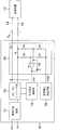
以下、この発明の実施例を図面に基づいて説明する。図1にこの発明の一実施例を示した。入力端子1には、適切な外部電源からの直流電圧が印加され、MOSFET等のスイッチング素子2に入力される。この入力端子1とスイッチング素子2との間には、平滑コンデンサC1が接地電位との間に接続されている。チョークコイル3と後述する電流検出抵抗R13との間を結ぶ出力ラインには、さらに平滑コンデンサC2が設けられている。スイッチング素子2は、ドライバ4でオン・オフ制御されて、入力した直流電流をパルス幅制御して出力し、ON時にスイッチング素子2より流入した電流およびOFF時に転流ダイオード20により流入した電流はチョークコイル3と平滑コンデンサC1の作用とあいまって、整流・平滑されて出力端子7側に出力される。チョークコイル3と出力端子7との間には電流検出抵抗R13が直列に挿入されている。正側の出力端子7と、負側の出力端子8との間には負荷19が接続されており、正側の出力端子7および負側の出力端子8から負荷19までのライン抵抗をそれぞれVRL,VRL’で表す。 Embodiments of the present invention will be described below with reference to the drawings. FIG. 1 shows an embodiment of the present invention. A DC voltage from an appropriate external power supply is applied to the input terminal 1 and input to the
また、電流検出抵抗R13と正側の出力端子7との間のラインには、直列に接続された分圧抵抗R11,R12が、当該ライン間と接地との間に接続されている。この分圧抵抗R11,R12の中間接続点から、分圧点電圧を出力する抵抗R8が設けられている。 Further, voltage dividing resistors R11 and R12 connected in series are connected between the current detection resistor R13 and the
さらに、前記電流検出抵抗R13の平滑コンデンサC2側にも、直列に接続された分圧抵抗R9,R10が前記出力ラインと接地との間に接続されている。そして、これらの分圧抵抗R9,R10の中間接続点からも分圧点電圧を取り出す抵抗R6が設けられている。ここで、抵抗R10は可変抵抗で構成されている。 Further, voltage dividing resistors R9 and R10 connected in series are also connected between the output line and the ground on the smoothing capacitor C2 side of the current detection resistor R13. A resistor R6 is also provided to extract a voltage dividing point voltage from an intermediate connection point between these voltage dividing resistors R9 and R10. Here, the resistor R10 is composed of a variable resistor.
こられの抵抗R6,R8で取り出された分圧点電圧は補正用アンプ6のそれぞれ減算入力、及び加算入力に入力される。補正用アンプ6の減算入力出力との間には増幅率を設定するフィードバック用の抵抗R5が接続され、加算入力からは分圧抵抗R7が接地されている。 The voltage dividing point voltages extracted by the resistors R6 and R8 are input to the subtraction input and the addition input of the correction amplifier 6, respectively. A feedback resistor R5 for setting an amplification factor is connected between the subtraction input output of the correction amplifier 6 and a voltage dividing resistor R7 is grounded from the addition input.
補正用アンプ6の出力は抵抗R4を介してさらにもう一つの補正用アンプ5の減算入力に入力され、この補正用アンプ5の加算入力には所定の基準電圧Vrefが印加される。さらに、チョークコイル3の出力側と補正用アンプ5の減算入力は抵抗R3で接続されている。The output of the correction amplifier 6 is input to the subtraction input of another correction amplifier 5 via the resistor R4, and a predetermined reference voltage Vref is applied to the addition input of the correction amplifier 5. Furthermore, the output side of the
補正用アンプ5の出力はスイッチング素子2を駆動するドライバ4に入力されてスイッチング素子2の導通率を制御する。こうした構成において、電流検出抵抗R13の両端に設けられた分圧抵抗R11,R12、およびR9,R10、さらにこれらの分圧点電圧を取り出す抵抗R6,R8、および補正用アンプ6とその分圧抵抗R7、フィードバック抵抗R5、および出力抵抗R4が、出力端7,8から先の負荷電流の変化に応じてインピーダンスの変化する回路となり(R’)、補正用アンプ5の正負入力値が一致して出力が0となるようにフィードバックし、スイッチング素子2を駆動するドライバ4への制御出力5を出力する補正用アンプ5の一方の入力である基準電圧Vrefに対するインピーダンス変化分に相応する補正入力Vref’となる。The output of the correction amplifier 5 is input to the driver 4 that drives the
またR10は可変抵抗であって、R’で示された負荷電流によって変化するインピーダンスの電圧ドロップ調整範囲を調整することができる。 R10 is a variable resistor, which can adjust the voltage drop adjustment range of the impedance that changes depending on the load current indicated by R '.
したがって、最終製品により異なる負荷インピーダンスによるラインドロップVRL、出力電流に対する電圧補正の係数を調整用抵抗R10により調整することができる。 Therefore, the line drop VRL with different load impedances depending on the final product and the voltage correction coefficient for the output current can be adjusted by the adjustment resistor R10.
またR13の設置位置については、図6に関連して説明したようにV0−GND間の分圧を図れば良く、負側の出力ラインであるR10,R12の接地端間に設けることもでき、回路設計の自由度がある。As for the installation position of R13, it is sufficient to divide the voltage between V0 and GND as described with reference to FIG. 6, and it can be provided between the ground terminals of R10 and R12 which are the negative output lines. There is a degree of freedom in circuit design.
さらにこの実施例では、図6のように、V0−GND間に抵抗を挿入し、電流検出には基準電圧を用いないため、分割抵抗には常にラインドロップに対して充分大きな電圧差を確保できる。また、検出抵抗Rは、出力ラインのプラス、マイナスのどちら側にも挿入することができるFurther, in this embodiment, as shown in FIG. 6, since a resistor is inserted between V0 and GND and a reference voltage is not used for current detection, a sufficiently large voltage difference with respect to the line drop is always secured in the dividing resistor. it can. The detection resistor R can be inserted on either the positive or negative side of the output line.
この実施例では、非絶縁型チョッパ方式を用いるものとしたが、トランスを用いた絶縁型の回路であっても同じ原理で補正することが可能であり、また電流検出は抵抗を用いる以外にもMOSFETのオン抵抗による電圧降下を検出する構成を用いることができる。 In this embodiment, the non-insulated chopper method is used. However, even an insulated circuit using a transformer can be corrected by the same principle, and the current detection is not limited to using a resistor. A configuration for detecting a voltage drop due to the on-resistance of the MOSFET can be used.
さらに、この実施例では、帰還抵抗のみで差分増幅器の増幅率を決めることができるため、特許文献2の構成と比べても負荷急変に対する応答性も優れている。 Furthermore, in this embodiment, since the amplification factor of the differential amplifier can be determined only by the feedback resistor, the response to a sudden load change is excellent as compared with the configuration of
この発明の実施例である、ラインドロップによる電圧降下補正回路の実施例は以上の通りであり、負荷に印加される出力電流を検出し、その電流値によって出力電圧を補正することで負荷端の電圧を一定に保つことができ、絶縁型、非絶縁型の電源を問わず、検出抵抗を出力ラインの正側、負側の何れにも接地可能で回路設計の自由度も高く、電圧変動時の応答性も高く、製品により異なる負荷インピーダンスに応じて、出力電流に対する電圧補正を行うことができる。 The embodiment of the voltage drop correction circuit by line drop, which is an embodiment of the present invention, is as described above. The output current applied to the load is detected, and the output voltage is corrected by the current value to correct the load end. The voltage can be kept constant, and the detection resistor can be grounded on either the positive side or the negative side of the output line, regardless of whether it is an isolated or non-isolated power supply. The voltage response to the output current can be corrected according to the load impedance that varies depending on the product.
また、負帰還抵抗のみで増幅器の増幅率を規定しているので、図7に示した負荷電流の変動に対しても、出力電圧の変動は実線で示したように応答性が高く、破線で例示した図4の従来例の構成に比べ、負荷電流変動の影響を受けにくい。 Further, since the amplification factor of the amplifier is defined only by the negative feedback resistor, the fluctuation of the output voltage is high in response to the fluctuation of the load current shown in FIG. Compared to the configuration of the conventional example shown in FIG. 4, it is less affected by load current fluctuations.
1 入力端子
2 スイッチング素子
3 チョークコイル
4 ドライバ
5 補正用アンプ
6 補正用アンプ
7,8 出力端子
9,10 ラインドロップ抵抗
11 負荷
12 平滑コンデンサ
R3,R4,R5,R6,R7,R8 抵抗
R9,R10,R11,R12 分圧抵抗
Vref 基準電圧DESCRIPTION OF SYMBOLS 1
Claims (4)
Translated fromJapanese正側又は負側の何れか一方の出力ライン中に直列に挿入されて、当該出力ライン中の出力電流を検出する電流検出抵抗と、
当該電流検出抵抗の両端から、負側又は正側の何れか一方の出力ラインとの間に設けられ、かつ各々直列接続された2つの抵抗からなる2組の分圧抵抗と、
負帰還抵抗を有する差分増幅器であって、前記2つの分圧抵抗の分圧点からの分圧電圧を各々入力して差分演算し、補正信号を生成する差分増幅回路と、
当該差分増幅回路から出力される補正信号を用い、前記電圧制御回路に供給される所定の基準電圧との差分演算を行い、当該電圧制御回路を制御することを特徴とする電圧降下補正回路。In the voltage drop correction circuit by line drop that detects the fluctuation of DC output voltage and feeds back to the voltage control circuit to stabilize the output voltage,
A current detection resistor inserted in series in either the positive side or negative side output line to detect the output current in the output line;
Two sets of voltage dividing resistors each including two resistors provided between both ends of the current detection resistor and either the negative side or the positive side output line, and connected in series,
A differential amplifier having a negative feedback resistor, wherein each of the divided voltages from the voltage dividing points of the two voltage dividing resistors is inputted to perform a difference calculation and generate a correction signal;
A voltage drop correction circuit for controlling the voltage control circuit by performing a difference operation with a predetermined reference voltage supplied to the voltage control circuit using a correction signal output from the difference amplifier circuit.
正側又は負側の何れか一方の出力ライン中に直列に挿入されて、当該出力ライン中の出力電流を検出する電流検出抵抗を備え、当該出力電流検出値でインピーダンスが変化する補正電流生成部で補正電流を生成し、制御回路に帰還して出力電圧を安定化するラインドロップによる電圧降下補正回路。Voltage drop correction by line drop that detects fluctuation of DC output voltage with voltage dividing resistor and feeds back error signal of this detected value and reference value to control circuit via error amplifier to stabilize output voltage In the circuit
A correction current generator that is inserted in series in either the positive or negative output line and includes a current detection resistor that detects the output current in the output line, and the impedance changes according to the output current detection value. A voltage drop correction circuit using a line drop that generates a correction current and feeds back to the control circuit to stabilize the output voltage.
上記出力ラインの正側又は負側の何れか一方の出力電流を検出し、当該検出電流による分圧回路のインピーダンス変動に基づく補整値を負帰還抵抗で増幅率を規定する差分増幅器で生成し、当該生成された補整値で所定の基準電圧と差分演算してドライバの制御を行うことを特徴とするラインドロップによる電圧降下補正回路の制御方法。The DC voltage supplied to the input terminal is chopped by the switching element, smoothed by the smoothing capacitor, supplied from the output terminal to the load, and the voltage dividing resistor connected to either the positive or negative output terminal The detected voltage fluctuation value is compared with the output current value detected by the current detection resistor inserted between the smoothing capacitor and the output terminal to generate a correction signal and control the driver of the switching element. In the control method of the voltage drop correction circuit by the line drop for correcting the output voltage,
The output current of either the positive side or the negative side of the output line is detected, and a compensation value based on the impedance fluctuation of the voltage dividing circuit due to the detected current is generated by a differential amplifier that defines an amplification factor with a negative feedback resistor, A control method of a voltage drop correction circuit by line drop, wherein the driver is controlled by calculating a difference with a predetermined reference voltage with the generated compensation value.
Priority Applications (1)
| Application Number | Priority Date | Filing Date | Title |
|---|---|---|---|
| JP2004370297AJP2006180603A (en) | 2004-12-22 | 2004-12-22 | Circuit for correcting voltage drop by line drop |
Applications Claiming Priority (1)
| Application Number | Priority Date | Filing Date | Title |
|---|---|---|---|
| JP2004370297AJP2006180603A (en) | 2004-12-22 | 2004-12-22 | Circuit for correcting voltage drop by line drop |
Publications (1)
| Publication Number | Publication Date |
|---|---|
| JP2006180603Atrue JP2006180603A (en) | 2006-07-06 |
Family
ID=36734173
Family Applications (1)
| Application Number | Title | Priority Date | Filing Date |
|---|---|---|---|
| JP2004370297APendingJP2006180603A (en) | 2004-12-22 | 2004-12-22 | Circuit for correcting voltage drop by line drop |
Country Status (1)
| Country | Link |
|---|---|
| JP (1) | JP2006180603A (en) |
Cited By (17)
| Publication number | Priority date | Publication date | Assignee | Title |
|---|---|---|---|---|
| JP2009232674A (en)* | 2008-02-26 | 2009-10-08 | Panasonic Electric Works Co Ltd | Power supply device |
| WO2010143605A1 (en)* | 2009-06-08 | 2010-12-16 | 株式会社ソニー・コンピュータエンタテインメント | Power supply circuit and power supply method |
| CN102067048A (en)* | 2008-06-17 | 2011-05-18 | 罗斯蒙德公司 | RF adapter for field device with variable voltage drop |
| EP2418763A2 (en) | 2010-08-09 | 2012-02-15 | OMRON Automotive Electronics Co., Ltd. | DC-DC converter |
| JP2012124865A (en)* | 2010-12-10 | 2012-06-28 | Fujitsu Telecom Networks Ltd | Power amplifier circuit and charge/discharge control device |
| JP2013153621A (en)* | 2012-01-26 | 2013-08-08 | Rohm Co Ltd | Power supply unit |
| US8538560B2 (en) | 2004-04-29 | 2013-09-17 | Rosemount Inc. | Wireless power and communication unit for process field devices |
| US8626087B2 (en) | 2009-06-16 | 2014-01-07 | Rosemount Inc. | Wire harness for field devices used in a hazardous locations |
| US8694060B2 (en) | 2008-06-17 | 2014-04-08 | Rosemount Inc. | Form factor and electromagnetic interference protection for process device wireless adapters |
| US8787848B2 (en) | 2004-06-28 | 2014-07-22 | Rosemount Inc. | RF adapter for field device with low voltage intrinsic safety clamping |
| US8929948B2 (en) | 2008-06-17 | 2015-01-06 | Rosemount Inc. | Wireless communication adapter for field devices |
| US9310794B2 (en) | 2011-10-27 | 2016-04-12 | Rosemount Inc. | Power supply for industrial process field device |
| US9674976B2 (en) | 2009-06-16 | 2017-06-06 | Rosemount Inc. | Wireless process communication adapter with improved encapsulation |
| US10761524B2 (en) | 2010-08-12 | 2020-09-01 | Rosemount Inc. | Wireless adapter with process diagnostics |
| JP2021182822A (en)* | 2020-05-19 | 2021-11-25 | ミツミ電機株式会社 | DC-DC converter, semiconductor integrated circuit for power supply control, and power supply device |
| CN114243630A (en)* | 2021-11-07 | 2022-03-25 | 中煤科工集团上海有限公司 | A safety control circuit for output power |
| JP2023031078A (en)* | 2021-08-24 | 2023-03-08 | キオクシア株式会社 | Memory system and control method |
Citations (4)
| Publication number | Priority date | Publication date | Assignee | Title |
|---|---|---|---|---|
| JPH0523214U (en)* | 1991-09-03 | 1993-03-26 | 富士電気化学株式会社 | Voltage drop compensation circuit for power load line |
| JPH1097328A (en)* | 1996-09-24 | 1998-04-14 | Sharp Corp | Stabilized power supply circuit and power supply device using the same |
| JP2001136734A (en)* | 1999-11-08 | 2001-05-18 | Fdk Corp | Overcurrent protection circuit |
| JP2003079139A (en)* | 2001-08-31 | 2003-03-14 | Victor Co Of Japan Ltd | Automatic switching constant current and constant voltage circuit |
- 2004
- 2004-12-22JPJP2004370297Apatent/JP2006180603A/enactivePending
Patent Citations (4)
| Publication number | Priority date | Publication date | Assignee | Title |
|---|---|---|---|---|
| JPH0523214U (en)* | 1991-09-03 | 1993-03-26 | 富士電気化学株式会社 | Voltage drop compensation circuit for power load line |
| JPH1097328A (en)* | 1996-09-24 | 1998-04-14 | Sharp Corp | Stabilized power supply circuit and power supply device using the same |
| JP2001136734A (en)* | 1999-11-08 | 2001-05-18 | Fdk Corp | Overcurrent protection circuit |
| JP2003079139A (en)* | 2001-08-31 | 2003-03-14 | Victor Co Of Japan Ltd | Automatic switching constant current and constant voltage circuit |
Cited By (23)
| Publication number | Priority date | Publication date | Assignee | Title |
|---|---|---|---|---|
| US8538560B2 (en) | 2004-04-29 | 2013-09-17 | Rosemount Inc. | Wireless power and communication unit for process field devices |
| US8787848B2 (en) | 2004-06-28 | 2014-07-22 | Rosemount Inc. | RF adapter for field device with low voltage intrinsic safety clamping |
| JP2009232674A (en)* | 2008-02-26 | 2009-10-08 | Panasonic Electric Works Co Ltd | Power supply device |
| CN102067048A (en)* | 2008-06-17 | 2011-05-18 | 罗斯蒙德公司 | RF adapter for field device with variable voltage drop |
| US8929948B2 (en) | 2008-06-17 | 2015-01-06 | Rosemount Inc. | Wireless communication adapter for field devices |
| US8847571B2 (en) | 2008-06-17 | 2014-09-30 | Rosemount Inc. | RF adapter for field device with variable voltage drop |
| US8694060B2 (en) | 2008-06-17 | 2014-04-08 | Rosemount Inc. | Form factor and electromagnetic interference protection for process device wireless adapters |
| US8996893B2 (en) | 2009-06-08 | 2015-03-31 | Sony Corporation | Power supply circuit for controlling power supply to an integrated circuit device with a rate of change of power supply voltage based on acquired value of current |
| CN102460885B (en)* | 2009-06-08 | 2014-09-03 | 索尼计算机娱乐公司 | Power supply circuit and power supply method |
| WO2010143605A1 (en)* | 2009-06-08 | 2010-12-16 | 株式会社ソニー・コンピュータエンタテインメント | Power supply circuit and power supply method |
| CN102460885A (en)* | 2009-06-08 | 2012-05-16 | 索尼计算机娱乐公司 | Power supply circuit and power supply method |
| US9674976B2 (en) | 2009-06-16 | 2017-06-06 | Rosemount Inc. | Wireless process communication adapter with improved encapsulation |
| US8626087B2 (en) | 2009-06-16 | 2014-01-07 | Rosemount Inc. | Wire harness for field devices used in a hazardous locations |
| US8829718B2 (en) | 2010-08-09 | 2014-09-09 | Omron Automotive Electronics Co., Ltd. | DC-DC converter |
| EP2418763A2 (en) | 2010-08-09 | 2012-02-15 | OMRON Automotive Electronics Co., Ltd. | DC-DC converter |
| US10761524B2 (en) | 2010-08-12 | 2020-09-01 | Rosemount Inc. | Wireless adapter with process diagnostics |
| JP2012124865A (en)* | 2010-12-10 | 2012-06-28 | Fujitsu Telecom Networks Ltd | Power amplifier circuit and charge/discharge control device |
| US9310794B2 (en) | 2011-10-27 | 2016-04-12 | Rosemount Inc. | Power supply for industrial process field device |
| JP2013153621A (en)* | 2012-01-26 | 2013-08-08 | Rohm Co Ltd | Power supply unit |
| JP2021182822A (en)* | 2020-05-19 | 2021-11-25 | ミツミ電機株式会社 | DC-DC converter, semiconductor integrated circuit for power supply control, and power supply device |
| JP7553769B2 (en) | 2020-05-19 | 2024-09-19 | ミツミ電機株式会社 | DC-DC converter, semiconductor integrated circuit for power supply control, and power supply device |
| JP2023031078A (en)* | 2021-08-24 | 2023-03-08 | キオクシア株式会社 | Memory system and control method |
| CN114243630A (en)* | 2021-11-07 | 2022-03-25 | 中煤科工集团上海有限公司 | A safety control circuit for output power |
Similar Documents
| Publication | Publication Date | Title |
|---|---|---|
| JP2006180603A (en) | Circuit for correcting voltage drop by line drop | |
| US7242169B2 (en) | Method and apparatus for voltage compensation for parasitic impedance | |
| US7294994B2 (en) | Power supply | |
| US7170267B1 (en) | Switching regulator with average current mode control | |
| CN106558987A (en) | Low quiescent current linear regulator circuit | |
| CN109478846B (en) | Power converter with robust stable feedback | |
| CN106936318B (en) | Load regulation apparatus and method for isolating an isolated output in a buck converter | |
| US8508200B2 (en) | Power supply circuit using amplifiers and current voltage converter for improving ripple removal rate and differential balance | |
| TWI643050B (en) | Voltage regulator | |
| TWI573006B (en) | Power supplier, power supply system, and voltage adjustment method | |
| US20060125455A1 (en) | Burst-mode switching voltage regulator with ESR compensation | |
| CN101247082B (en) | Detection circuit, power supply system and control method | |
| TW201901163A (en) | Current sensor circuit | |
| US7193871B2 (en) | DC-DC converter circuit | |
| CN109782053B (en) | Power supply device | |
| US20050035746A1 (en) | Voltage regulator with adjustable output impedance | |
| US10491119B2 (en) | Combined high side and low side current sensing | |
| JP5287205B2 (en) | Power supply circuit and operation control method thereof | |
| US7705578B2 (en) | Switching regulator | |
| JP6711730B2 (en) | Power supply | |
| JP2005251130A (en) | Voltage regulator circuit with short circuit protection circuit | |
| WO2007099489A2 (en) | Improved window comparator with accurate levels for use in dc-dc converters | |
| US20210365058A1 (en) | Analog front end with pulse width modulation current compensation | |
| JP4378530B2 (en) | DC power supply controller | |
| JP2006217695A (en) | Switching power supply |
Legal Events
| Date | Code | Title | Description |
|---|---|---|---|
| A621 | Written request for application examination | Free format text:JAPANESE INTERMEDIATE CODE: A621 Effective date:20060907 | |
| A977 | Report on retrieval | Free format text:JAPANESE INTERMEDIATE CODE: A971007 Effective date:20090409 | |
| A131 | Notification of reasons for refusal | Free format text:JAPANESE INTERMEDIATE CODE: A131 Effective date:20090508 | |
| A02 | Decision of refusal | Free format text:JAPANESE INTERMEDIATE CODE: A02 Effective date:20090911 |