JP2006179895A - Suction method - Google Patents
Suction methodDownload PDFInfo
- Publication number
- JP2006179895A JP2006179895AJP2005354067AJP2005354067AJP2006179895AJP 2006179895 AJP2006179895 AJP 2006179895AJP 2005354067 AJP2005354067 AJP 2005354067AJP 2005354067 AJP2005354067 AJP 2005354067AJP 2006179895 AJP2006179895 AJP 2006179895A
- Authority
- JP
- Japan
- Prior art keywords
- electrodes
- substrate
- adsorption
- electrode
- adsorption device
- Prior art date
- Legal status (The legal status is an assumption and is not a legal conclusion. Google has not performed a legal analysis and makes no representation as to the accuracy of the status listed.)
- Granted
Links
- 238000000034methodMethods0.000titleclaimsdescription15
- 239000000758substrateSubstances0.000claimsabstractdescription137
- 230000005684electric fieldEffects0.000claimsabstractdescription23
- 238000001179sorption measurementMethods0.000claimsdescription136
- 230000001681protective effectEffects0.000claimsdescription19
- 239000012212insulatorSubstances0.000description17
- 239000010408filmSubstances0.000description10
- 239000003990capacitorSubstances0.000description8
- 238000004544sputter depositionMethods0.000description8
- 229910052751metalInorganic materials0.000description7
- 239000002184metalSubstances0.000description7
- 239000011810insulating materialSubstances0.000description4
- 239000010409thin filmSubstances0.000description4
- 239000011521glassSubstances0.000description3
- 238000005477sputtering targetMethods0.000description3
- 239000000126substanceSubstances0.000description3
- 229910018072Al 2 O 3Inorganic materials0.000description2
- 239000004642PolyimideSubstances0.000description2
- 239000000919ceramicSubstances0.000description2
- 238000001816coolingMethods0.000description2
- 238000005468ion implantationMethods0.000description2
- TWNQGVIAIRXVLR-UHFFFAOYSA-Noxo(oxoalumanyloxy)alumaneChemical compoundO=[Al]O[Al]=OTWNQGVIAIRXVLR-UHFFFAOYSA-N0.000description2
- 230000002093peripheral effectEffects0.000description2
- 229920001721polyimidePolymers0.000description2
- HBMJWWWQQXIZIP-UHFFFAOYSA-Nsilicon carbideChemical compound[Si+]#[C-]HBMJWWWQQXIZIP-UHFFFAOYSA-N0.000description2
- 229910010271silicon carbideInorganic materials0.000description2
- 229920002379silicone rubberPolymers0.000description2
- 239000004945silicone rubberSubstances0.000description2
- 229910017083AlNInorganic materials0.000description1
- GYHNNYVSQQEPJS-UHFFFAOYSA-NGalliumChemical compound[Ga]GYHNNYVSQQEPJS-UHFFFAOYSA-N0.000description1
- VYPSYNLAJGMNEJ-UHFFFAOYSA-NSilicium dioxideChemical compoundO=[Si]=OVYPSYNLAJGMNEJ-UHFFFAOYSA-N0.000description1
- XUIMIQQOPSSXEZ-UHFFFAOYSA-NSiliconChemical compound[Si]XUIMIQQOPSSXEZ-UHFFFAOYSA-N0.000description1
- 230000000274adsorptive effectEffects0.000description1
- 229910052785arsenicInorganic materials0.000description1
- RQNWIZPPADIBDY-UHFFFAOYSA-Narsenic atomChemical compound[As]RQNWIZPPADIBDY-UHFFFAOYSA-N0.000description1
- 230000015572biosynthetic processEffects0.000description1
- 239000003575carbonaceous materialSubstances0.000description1
- 230000015556catabolic processEffects0.000description1
- PMHQVHHXPFUNSP-UHFFFAOYSA-Mcopper(1+);methylsulfanylmethane;bromideChemical compoundBr[Cu].CSCPMHQVHHXPFUNSP-UHFFFAOYSA-M0.000description1
- 239000013078crystalSubstances0.000description1
- 239000010432diamondSubstances0.000description1
- 229910003460diamondInorganic materials0.000description1
- 238000005530etchingMethods0.000description1
- 230000004907fluxEffects0.000description1
- 229910052733galliumInorganic materials0.000description1
- 239000004973liquid crystal related substanceSubstances0.000description1
- 239000000463materialSubstances0.000description1
- 229910003465moissaniteInorganic materials0.000description1
- 238000005240physical vapour depositionMethods0.000description1
- 229920001296polysiloxanePolymers0.000description1
- 239000004065semiconductorSubstances0.000description1
- -1sialonSubstances0.000description1
- 229910052710siliconInorganic materials0.000description1
- 239000010703siliconSubstances0.000description1
- 230000007723transport mechanismEffects0.000description1
Images


Landscapes
- Physical Vapour Deposition (AREA)
- Chemical Vapour Deposition (AREA)
- Container, Conveyance, Adherence, Positioning, Of Wafer (AREA)
Abstract
Description
Translated fromJapanese本発明は、吸着装置にかかり、特に、絶縁性の基板を吸着できる吸着装置に関する。 The present invention relates to an adsorption device, and more particularly to an adsorption device capable of adsorbing an insulating substrate.
従来より、真空装置内で基板を保持するために、静電吸着装置が使用されている。
図8(a)の符号101は、スパッタリング装置であり、真空槽110を有している。該真空槽110内の天井側にはターゲット102が配置されており、底壁側には吸着装置104が配置されている。Conventionally, an electrostatic chuck is used to hold a substrate in a vacuum apparatus.
A
この吸着装置104は、誘電体121と、該誘電体121内に埋め込まれた一対の電極1221、1222とを有しており、誘電体121に形成された孔内に、下側からリフトピン106が挿通されている。The
各電極1221、1222は、真空槽110外部に配置されたチャック用電源109にそれぞれ接続されている。Each electrode 1221, 1222 are connected to a
吸着装置104上に基板112を配置すると、基板112は、基板112と電極1221、1222間に存する厚さ数10〜数100μmの誘電体121の層を介して、各電極1221、1222と平行に対向する。When the
基板112がシリコンウェハーやガリウム・ひ素ウェハーの場合、基板112は導電性を有している。従って、吸着装置104上に基板112が配置されると、一方の電極1221と基板112の間に、同図(b)の符号1251で示すコンデンサが形成され、また、他方の電極1222と基板112の間にも、同図(b)の符号1252で示すコンデンサが形成される。When the
この2つのコンデンサ1251、1252は、電源109に対して互いに直列接続されており、一方の電極1221に正電圧、他方の電極1222に負電圧を印加すると、コンデンサ1251、1252が充電され、基板112と一方の電極1221の間、及び基板112と他方の電極1222の間に生じる静電吸着力によって基板112が吸着装置104の表面に静電吸着される。These two capacitors 1251 , 1252 are connected in series to the
静電吸着された状態では、基板112は吸着装置104上に密着されており、基板112と吸着装置104間の熱伝達率が大きくなり、吸着装置104内に設けられたヒータや冷却装置によって基板112を所望温度に制御することが可能になる。従って、ターゲット102をスパッタリングし、基板112表面に薄膜を形成する際に、薄膜の成長温度を精密に制御することができる。 In the electrostatically attracted state, the
薄膜形成プロセスが終了すると、電極1221、1222への電圧印加を終了させ、基板112の吸着を解除してリフトピン106を上昇させると、基板112を吸着装置104上から持ち上げ、真空槽110外に搬出する。When the thin film formation process is finished, the voltage application to the electrodes 1221 and 1222 is finished, the suction of the
上記のように、従来技術の吸着装置104では、基板112を電極とし、吸着装置104内部に配置された電極1221、1222との間でコンデンサ1251、1252を形成し、静電吸着力を発生させている。従って、この吸着装置104が静電吸着できる基板112は導電性を有している必要がある。As described above, in the prior art of the
しかしながら近年では、液晶表示装置やプラズマディスプレイ装置を構成させるガラス基板を吸着しながら真空処理したいという要求がある。 However, in recent years, there is a demand for vacuum processing while adsorbing a glass substrate constituting a liquid crystal display device or a plasma display device.
半導体の単結晶から成る基板の場合、抵抗値が大きいものの導電性を有しているため静電吸着力が発生するが、ガラス基板の場合には絶縁性が高いため、図8(b)のコンデンサが形成されず、静電チャック104上に静電吸着することができない。 In the case of a substrate made of a semiconductor single crystal, although it has a large resistance value, it has electrical conductivity, and therefore, an electrostatic attracting force is generated. However, in the case of a glass substrate, the insulating property is high, so that FIG. A capacitor is not formed and cannot be electrostatically adsorbed on the
本発明は上記従来技術の課題を解決するために創作されたものであり、その目的は、絶縁性の基板を吸着できる吸着装置を提供することにある。 The present invention was created in order to solve the above-described problems of the prior art, and an object thereof is to provide an adsorption device capable of adsorbing an insulating substrate.
上述したように、従来技術の静電吸着装置の場合、シリコーンウェハ等の導電性を有する基板を静電吸着するために、Al2O3、AlN、SiC、ポリイミド、シリコーンゴム等の高誘電率の絶縁材料が電極と基板の間に配置されている(絶縁材料を配置しないと電極間が短絡してしまう)。As described above, in the case of the electrostatic adsorption device of the prior art, a high dielectric constant such as Al2 O3 , AlN, SiC, polyimide, and silicone rubber is used to electrostatically adsorb a conductive substrate such as a silicone wafer. The insulating material is disposed between the electrode and the substrate (if the insulating material is not disposed, the electrodes are short-circuited).
従って、基板と電極との間にはコンデンサが形成され、クーロン力が発生する。そのクーロン力による吸着力Fは、絶縁材料の誘電率や表面状態に依存する係数をa、基板と電極間の距離をd(詳しくは絶縁材料の厚さ、又は基板と静電チャック表面間のギャップを言う)と基板、電極と基板の間の電圧をVとすると、次式で表わせる。
F = 1/2・a・(V/d)2Therefore, a capacitor is formed between the substrate and the electrode, and a Coulomb force is generated. The adsorption force F due to the Coulomb force is a coefficient depending on the dielectric constant and surface state of the insulating material, and a distance between the substrate and the electrode d (specifically, the thickness of the insulating material or between the substrate and the electrostatic chuck surface). When the voltage between the substrate and the electrode and the substrate is V, it can be expressed by the following equation.
F = 1/2 · a · (V / d)2
しかし、ガラスのような絶縁性基板の場合には、基板と電極間にはコンデンサが形成されないため、上記のようなクーロン力による静電吸着力Fは発生しない。
他方、分極率がαである絶縁性の物質が電場E中に配置された場合、その物質には、単位体積当たり下記のようなグラディエント力fが働くことが知られている。
f = 1/2・α・grad(E2)
本発明の発明者等は、グラディエント力fに着目し、絶縁性の基板も吸着できる吸着装置を発明するに至ったのである。However, in the case of an insulating substrate such as glass, a capacitor is not formed between the substrate and the electrode, so that the electrostatic adsorption force F due to the Coulomb force as described above does not occur.
On the other hand, when an insulating substance having a polarizability α is arranged in the electric field E, it is known that the following gradient force f acts on the substance per unit volume.
f = 1/2 · α · grad (E2 )
The inventors of the present invention have focused on the gradient force f and have invented an adsorption device that can also adsorb an insulating substrate.
即ち、誘電体(絶縁性物質)ではα>0であるから、上式によると絶縁性の基板は電場の強い方に引きつけられることになる。 That is, since α> 0 in the dielectric (insulating substance), according to the above formula, the insulating substrate is attracted to the stronger electric field.
図7の符号80は、基板83に対し、正電圧と負電圧が印加される電極81、82間に形成される電場を示しており、電極81、82付近では電場が強く、遠い位置では弱いため、基板83には、電極81、82の方向に向いた力fが働いている。
また、上式によると、grad(E2)が大きい方が基板に大きなグラディエント力fが働くから、Eの空間変化率が大きい程、グラディエント力fも大きくなる。Further, according to the above equation, the greater the grad (E2 ), the greater the gradient force f acts on the substrate. Therefore, the greater the spatial change rate of E, the greater the gradient force f.
従って、電極の配置を工夫し、電場の変化率が、基板付近で小さく、電極付近で大きくなるようにすると、基板83に大きなグラディエント力fが働くようになる。Therefore, when the arrangement of the electrodes is devised so that the rate of change of the electric field is small near the substrate and large near the electrode, a large gradient force f acts on the
具体的には、吸着装置が配置される真空槽の電位をゼロ(接地電位)とした場合、正電圧を印加する電極と負電圧を印加する電極とを近接して隣り合わせに配置すればよい。 Specifically, when the potential of the vacuum chamber in which the adsorption device is disposed is set to zero (ground potential), an electrode to which a positive voltage is applied and an electrode to which a negative voltage is applied may be disposed adjacent to each other.
また、電極間に形成される電場を考えると、電極付近に誘電体があった場合には、電束は誘電体(比誘電率εr>1)に引き込まれる。従って、吸着装置の電極と基板との間に誘電体が配置されていると、電気力線は誘電体に引き込まれ易くなり、その結果、基板と電極の間が真空である場合に比べて電場(電気力線の密度)が小さくなってしまう。 Considering the electric field formed between the electrodes, if there is a dielectric near the electrodes, the electric flux is drawn into the dielectric (relative permittivity εr> 1). Therefore, if a dielectric is disposed between the electrode of the adsorption device and the substrate, the electric lines of force are more easily drawn into the dielectric, and as a result, the electric field is larger than when the space between the substrate and the electrode is a vacuum. (Density of electric lines of force) becomes small.
従って、その逆に誘電体上に誘電体を配置しなければgrad(E2)が大きくなり、その結果、大きな吸着力(グラディエント力f)を得ることが可能になる。Accordingly, if the dielectric is not disposed on the dielectric, grad (E2 ) increases, and as a result, a large adsorption force (gradient force f) can be obtained.
図7のような正負電圧を印加する電極81、82上に誘電体層を配置した場合と配置しない場合とで、絶縁性の基板83に働く吸着力を測定した。 The adsorption force acting on the
電極81、82の幅は4mm、電極81、82の間隔は1mm、吸着面の直径は8インチである。比較のために用いた誘電体はAl2O3を主成分とするセラミックスであり、その厚みは500μm、抵抗率は約1011Ω・cmのものである。The width of the
吸着対象物は直径8インチ、厚さ5mmの透明石英ガラスから成る基板であり、その抵抗率は1.0×10¹⁸Ωcm、比誘電率は3.70(0〜1MHz)である。Adsorption object is a substrate made of a diameter of 8 inches and a thickness of 5mm transparent quartz glass, its resistivity is 1.0 × 10¹⁸ Ωcm, the dielectric constant is 3.70 (0~1MHz).
吸着力を測定した結果を下記表1に示す。基板と電極81、82の間に誘電体が存しない場合には、1.5倍程度の吸着力が得られている。 The results of measuring the adsorption force are shown in Table 1 below. When there is no dielectric between the substrate and the

このように、本発明は従来技術が常識としていた電極上の誘電体層に着目して創作されたものであり、その請求項1に記載された発明は、吸着装置であって、板状の基体と、前記基体表面に互いに絶縁した状態で配置され、第1の電圧が印加される第1の電極と、前記第1の電圧とは異なる第2の電圧が印加される第2の電極とを有することを特徴とする。 As described above, the present invention was created by paying attention to the dielectric layer on the electrode, which has been common knowledge in the prior art, and the invention described in
この基体は、絶縁性の板で構成してもよいし、金属板上に絶縁性の膜を形成して構成することができる。絶縁性の膜は、酸化アルミニウム、窒化アルミニウム、炭化珪素、サイアロン、ダイヤモンド、ポリイミド、シリコーンゴム等の材料を用いることができる。 This substrate may be formed of an insulating plate or may be formed by forming an insulating film on a metal plate. For the insulating film, materials such as aluminum oxide, aluminum nitride, silicon carbide, sialon, diamond, polyimide, and silicone rubber can be used.
吸着装置が配置される真空槽を接地電位とした場合、第1、第2の電極に電圧を印加する電源を、第1、第2の電極のいずれか一方に正電圧、他方に負電圧を印加できるように構成しておくとよい。
この請求項1記載の吸着装置の場合には、請求項2に記載したように、前記吸着装置の前記第1、第2の電極が配置された表面に基板を配置すると、前記基板は前記第1、第2の電極と接触するように構成することができる。
また、請求項1記載の吸着装置の場合には、請求項3に記載したように、前記第1、第2の電極間に、絶縁性の突部を配置することができる。
更にまた、請求項1記載の吸着装置の場合には、請求項4に記載したように、前記基体の表面と前記第1、第2の電極の表面とを同一平面に構成することもできる。
以上の請求項1乃至請求項5のいずれか1項記載の吸着装置については、請求項5に記載したように、前記第1、第2の前記電極表面を露出させておくことができる。
他方、請求項1乃至請求項5のいずれか1項記載の吸着装置については、請求項6に記載したように、前記第1、第2の電極表面に保護膜を形成しておくこともできる。
この保護膜が導電性を有している場合には、導電性保護膜が電極の上のみを覆うか、又は菱電曲が短絡しないように保護膜を付けると、第1、第2の電極は露出しているのと同じ状態であり、保護膜が絶縁性の場合は第1、第2の電極表面は露出しなくなる。この場合、保護膜はPVD、CVD、イオン注入などによって形成でき、その厚さは吸着力を低下させないために500μm以下が望ましい。
請求項1乃至請求項6のいずれか1項記載の吸着装置の場合には、請求項7に記載したように、前記第1、第2の電極間の間隔は2mm以下にしておくとよい。
また、請求項1乃至請求項7のいずれか1項記載の吸着装置については、請求項8に記載したように、前記第1、第2の電極の幅を4mm以下にしておくことができる。
また、請求項1乃至請求項8のいずれか1項に記載された吸着装置が、前記第1の電極と前記第2の電極とが複数本配置されている場合には、請求項9に記載したように、前記第1の電極と前記第2の電極とを交互に配置する領域を設けることができる。
更に、請求項1乃至請求項9のいずれか1項記載の吸着装置については、請求項10に記載したように、前記第1、第2の電圧とは異なる第3の電圧が印加される第3の電極を設けることができる。
他方、真空槽を有する真空処理装置の場合、該真空槽内に請求項1乃至請求項9のいずれか1項記載の吸着装置を配置し、請求項11に記載した真空処理装置を構成することができる。
この場合、請求項12に記載したように、電源を設け、該電源により、少なくとも前記第1、第2の電極間に1.0×10⁶V/m以上の電界を形成できるように構成することができる。
また、請求項11又は請求項12のいずれか1項記載の真空処理装置については、請求項13に記載したように、前記吸着装置周囲に保護板を配置し、前記吸着装置上に基板を配置すると、前記基板は前記保護板内に収容されるように構成することができる。
この真空処理装置では、基板裏面と吸着装置の間に形成される隙間内にプラズマが侵入しないので、電極間が短絡するおそれはない。When the vacuum chamber in which the adsorption device is disposed is set to the ground potential, a power source for applying a voltage to the first and second electrodes is set to a positive voltage on one of the first and second electrodes, and a negative voltage is applied to the other. It may be configured so that it can be applied.
In the case of the adsorption device according to the first aspect, as described in the second aspect, when the substrate is disposed on the surface of the adsorption device where the first and second electrodes are disposed, the substrate is It can be configured to contact the first and second electrodes.
In the case of the adsorption device according to
Furthermore, in the case of the adsorption device according to the first aspect, as described in the fourth aspect, the surface of the substrate and the surfaces of the first and second electrodes can be configured in the same plane.
In the adsorption device according to any one of
On the other hand, in the adsorption device according to any one of
When this protective film has conductivity, the first and second electrodes can be formed by covering the electrode only, or by attaching a protective film so that the rhomboid does not short-circuit. Is the same as that exposed, and when the protective film is insulating, the surfaces of the first and second electrodes are not exposed. In this case, the protective film can be formed by PVD, CVD, ion implantation, etc., and its thickness is preferably 500 μm or less so as not to reduce the adsorption power.
In the case of the adsorption device according to any one of
In the adsorption device according to any one of
Moreover, when the adsorption apparatus described in any one of
Further, in the adsorption device according to any one of
On the other hand, in the case of a vacuum processing apparatus having a vacuum tank, the suction apparatus according to any one of
In this case, as described in
Moreover, about the vacuum processing apparatus of any one of
In this vacuum processing apparatus, since plasma does not enter into the gap formed between the back surface of the substrate and the adsorption device, there is no possibility that the electrodes are short-circuited.
請求項14記載の発明は、板状の基体と、前記基体上に配置され、第1の電圧が印加される第1の電極と、前記第1の電圧とは異なる第2の電圧が印加される第2の電極とを有し、絶縁性の吸着対象基板を吸着するように構成された吸着装置であって、前記第1、第2の電極は表面が露出され、前記第1、第2の電極間の距離と、前記第1、第2の電極と吸着対象基板との間の距離とは、前記吸着対象基板が不均一電界によるグラジエント力によって吸着される大きさに設定された吸着装置である。
請求項15記載の発明は、請求項14記載の吸着装置であって、前記第1、第2の電極は、前記吸着対象基板と接触するように配置された吸着装置である。
請求項16記載の発明は、請求項15記載の吸着装置であって、前記基体の表面と前記第1、第2の電極の表面とは同一平面に形成された吸着装置である。
請求項17記載の発明は、請求項14記載の吸着装置であって、前記第1、第2の電極間には絶縁性の突部が配置され、前記吸着対象基板と前記第1、第2の電極とは非接触に構成された吸着装置である。
請求項18記載の発明は、請求項14記載の吸着装置であって、前記第1、第2の電極の上端部は、前記基体の表面よりも低く形成され、前記吸着対象基板と前記基体表面とが接触するように構成された吸着装置である。
請求項19記載の発明は、請求項14乃至請求項18のいずれか1項記載の吸着装置であって、前記第1、第2の電極と前記吸着対象基板の間の距離は500×10-6m以下にされた吸着装置である。
請求項20記載の発明は、請求項14乃至請求項19のいずれか1項記載の吸着装置であって、前記第1、第2の電極間の間隔は2mm以下にされた吸着装置である。
請求項21記載の発明は、請求項14乃至請求項20のいずれか1項記載の吸着装置であって、前記第1、第2の電極の幅は4mm以下にされた吸着装置である。
請求項22記載の発明は、請求項14乃至請求項21のいずれか1項記載の吸着装置であって、前記第1の電極と前記第2の電極とが複数本配置された吸着装置であって、前記第1の電極と前記第2の電極とが交互に配置された領域を有する吸着装置である。
請求項23記載の発明は、請求項14乃至請求項22のいずれか1項記載の吸着装置であって、前記第1、第2の電圧とは異なる第3の電圧が印加される第3の電極を有する吸着装置である。
請求項24記載の発明は、真空槽を有し、該真空槽内に請求項14乃至請求項23のいずれか1項記載の吸着装置が配置された真空処理装置である。
請求項25記載の発明は、請求項24記載の真空処理装置であって、電源を有し、該電源により、少なくとも前記第1、第2の電極間に1.0×10⁶V/m以上の電界を形成できるように構成された真空処理装置である。
請求項26記載の発明は、請求項24又は請求項25のいずれか1項記載の真空処理装置であって、前記吸着装置周囲に保護板が配置され、前記吸着装置上に基板を配置すると、前記基板は前記保護板内に収容されるように構成された真空処理装置である。
請求項27記載の発明は、絶縁性の板状の基体上に、第1、第2の電極が交互に配置された吸着装置の、前記第1、第2の電極上に絶縁基板を配置し、前記第1、第2の電極に電圧を印加し、前記絶縁基板を吸着する吸着方法であって、前記第1、第2の電極間に1.0×10⁶V/m以上の電界を発生させ、前記絶縁基板をグラディエント力によって吸着する吸着方法である。
請求項28記載の発明は、請求項27記載の吸着方法であって、前記第1、第2の電極の電極幅を4mm以下、電極間隔を2mm以下とする吸着方法である。
請求項29記載の発明は、請求項27又は請求項28のいずれか1項記載の吸着方法であって、前記絶縁基板と前記基体の間に突起を配置し、前記第1、第2の電極と前記絶縁基板とを非接触の状態にして前記電圧を印加する吸着方法である。
請求項30記載の発明は、請求項27乃至請求項29のいずれか1項記載の吸着方法であって、前記第1、第2の電極表面に、予め保護膜を形成しておく吸着方法である。
請求項31記載の発明は、請求項27乃至請求項30のいずれか1項記載の吸着方法であって、前記第1、第2の電極と前記絶縁基板との間の距離を、500×10-6m以下にして前記電圧を印加する吸着方法である。According to the fourteenth aspect of the present invention, a plate-like substrate, a first electrode disposed on the substrate, to which a first voltage is applied, and a second voltage different from the first voltage are applied. The first and second electrodes are exposed at their surfaces, and the first and second electrodes are exposed to each other. The distance between the electrodes and the distance between the first and second electrodes and the adsorption target substrate are set to such a size that the adsorption target substrate is adsorbed by a gradient force due to a non-uniform electric field. It is.
A fifteenth aspect of the present invention is the adsorption apparatus according to the fourteenth aspect, wherein the first and second electrodes are arranged so as to contact the adsorption target substrate.
A sixteenth aspect of the present invention is the adsorption apparatus according to the fifteenth aspect, wherein the surface of the substrate and the surfaces of the first and second electrodes are formed on the same plane.
The invention according to claim 17 is the suction device according to claim 14, wherein an insulating protrusion is disposed between the first and second electrodes, and the suction target substrate and the first and second electrodes are arranged. This electrode is a non-contact adsorption device.
The invention according to
The invention according to
A twentieth aspect of the invention is the adsorption device according to any one of the fourteenth to nineteenth aspects, wherein the distance between the first and second electrodes is 2 mm or less.
A twenty-first aspect of the present invention is the adsorption apparatus according to any one of the fourteenth to twentieth aspects, wherein the first and second electrodes have a width of 4 mm or less.
A twenty-second aspect of the present invention is the adsorption apparatus according to any one of the fourteenth to twenty-first aspects, wherein a plurality of the first electrodes and the second electrodes are arranged. The adsorption device has a region in which the first electrode and the second electrode are alternately arranged.
A twenty-third aspect of the present invention is the adsorption device according to any one of the fourteenth to twenty-second aspects, wherein a third voltage different from the first and second voltages is applied. An adsorption device having an electrode.
A twenty-fourth aspect of the present invention is a vacuum processing apparatus having a vacuum chamber, wherein the suction device according to any one of the fourteenth to twenty-third aspects is disposed in the vacuum chamber.
A twenty-fifth aspect of the invention is the vacuum processing apparatus according to the twenty-fourth aspect, comprising a power source, and at least 1.0 × 10⁶ V / m or more between the first and second electrodes by the power source. It is a vacuum processing apparatus comprised so that the electric field of this can be formed.
The invention according to
According to a twenty-seventh aspect of the present invention, an insulating substrate is disposed on the first and second electrodes of the adsorption device in which the first and second electrodes are alternately disposed on an insulating plate-like substrate. An adsorption method in which a voltage is applied to the first and second electrodes to adsorb the insulating substrate, and an electric field of 1.0 × 10⁶ V / m or more is applied between the first and second electrodes. This is an adsorption method in which the insulating substrate is adsorbed by a gradient force.
A twenty-eighth aspect of the present invention is the adsorption method according to the twenty-seventh aspect, wherein the first and second electrodes have an electrode width of 4 mm or less and an electrode interval of 2 mm or less.
A twenty-ninth aspect of the present invention is the adsorption method according to any one of the twenty-seventh or twenty-eighth aspects, wherein a protrusion is disposed between the insulating substrate and the base, and the first and second electrodes are arranged. And the insulating substrate in a non-contact state and applying the voltage.
A thirty-third aspect of the invention is the adsorption method according to any one of the twenty-seventh to twenty-ninth aspects, wherein a protective film is formed in advance on the first and second electrode surfaces. is there.
A thirty-first aspect of the invention is the adsorption method according to any one of the twenty-seventh to thirty-third aspects, wherein a distance between the first and second electrodes and the insulating substrate is set to 500 × 10. It is an adsorption method in which the voltage is applied at-6 m or less.
真空雰囲気中で絶縁性の基板を吸着することができる。 An insulating substrate can be adsorbed in a vacuum atmosphere.
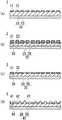
本発明の真空処理装置の一例を図1(a)の符号70に示す。
この真空処理装置70は、真空槽72と、チャック用電源73と、スパッタ用電源75と、チャック用電源73及びスパッタ用電源75のコントローラ(コンピュータ)74とを有している。An example of the vacuum processing apparatus of the present invention is indicated by
The
真空槽72内には、スパッタリングターゲット76と、本発明の第一例の吸着装置1が配置されている。吸着装置1の平面図を図2(a)に示し、そのA−A線断面図を同図(b)に示す。 In the
この吸着装置1は、板状の基体10を有している。基体10は、金属板18と、該金属板18表面に配置された絶縁体19とで構成されている。絶縁体19は、酸化アルミニウム等の絶縁性のセラミックスの層で構成されている。 The
絶縁体19表面には、導電性のカーボン材から成る第1、第2の電極11、12が設けられている。従って、第1、第2の電極11、12表面は、基体10表面よりも突き出されている。 First and
第1、第2の電極11、12は、櫛状にパターニングされており、非接触の状態で櫛の歯部分が互いに噛み合うように配置されている。 The first and
基体10の直径は8インチ、第1、第2の電極11、12の幅は4mm、電極間の間隔は1mmである。 The diameter of the
このような真空処理装置70を用いて真空処理を行う場合、先ず、真空槽72内を真空状態にし、図示しない基板搬送機構によって真空槽72内に基板を搬入し、基板を吸着装置1表面に配置する。 When performing vacuum processing using such a
図1(b)は、吸着装置1の部分の拡大図であり、同図の符号7は、吸着装置1上に配置された絶縁性の基板を示している。 FIG. 1B is an enlarged view of a portion of the
基板7が吸着装置1上に配置されると、基板7の裏面と第1、第2の電極表面とが接触する。この状態では基板7裏面と絶縁体19表面との間は離間しており、隙間が形成されている。 When the
吸着装置1の周囲にはリング状の保護板9が配置されており、基板7を吸着装置1上に載置すると、基板7の外周部分が保護板9の内周面と接触し、基板7裏面と絶縁体19の間に形成された隙間は保護板9によって密閉された状態になる。 A ring-shaped
チャック用電源73は、第1、第2の電極11、12に接続されており、真空槽72を接地電位に置き、チャック用電源73を起動し、第1、第2の電極11、12のうちの一方に負電圧、他方に正電圧を印加すると、第1、第2の電極11、12間に電界が形成される。 The
図4は、真空槽72を接地電位に置き、第1の電極11に正電圧、第2の電極12に負電圧を印加した場合に、基板7と第1、第2の電極11、12間に形成される電場E、及び基板7に働く力fを模式的に示した図である。基板7は絶縁性が高いため、第1、第2の電極11、12間には殆ど電流は流れない。 FIG. 4 shows that when the
基板7を吸着装置1に吸着した状態で真空槽72内にスパッタリングガスを導入し、スパッタ用電源75を起動し、スパッタリングターゲットに高電圧を印加すると、スパッタリングターゲット表面近傍にプラズマが形成され、スパッタリングが始まる。 When the sputtering gas is introduced into the
基板7は吸着装置1上に吸着されているので、基板7と吸着装置1との間の熱伝導率が高いので、基体10内や基体10の裏面にヒータや冷却装置を設けておくと、基板7の温度を制御しながら薄膜を形成することが可能になる。 Since the
また、基板7周囲には保護板9が配置されているので、スパッタリングの際に真空槽70内に形成されたプラズマは、基板7裏面と基体10の間に形成される隙間内に侵入しない。従って、第1の電極11と第2の電極12の間にはプラズマがなく、第1、第2の電極間がプラズマによって短絡することがない。 Further, since the
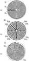
第一例の吸着装置1の模式的な断面図を図3(a)に示す。この吸着装置1では、第1、第2の電極11、12は絶縁体19上に形成されており、電極表面は絶縁体表面よりも高くなっている。 A schematic cross-sectional view of the
同図(b)〜(d)に、第二例〜第四例の吸着装置2〜4を示す。
第二例〜第四例の吸着装置2〜4は、金属板28、38、48をそれぞれ有している。The adsorption | suction apparatuses 2-4 of a 2nd example-a 4th example are shown to the same figure (b)-(d).
The
各金属板28、38、48上には、絶縁体29、39、49が配置されており、これらの絶縁体29、39、49表面には、底部が金属板28、38に達しないように凹部26、36、46が形成されている。
各絶縁体29、39、49の凹部26、36、46には、第1、第2の電極21、21、31、32、41、42が互いに絶縁した状態で配置されている。第1、第2の電極21、21、31、32、41、42の下端部は、各凹部26、36、46の底面上に配置されている。 The first and
同図(b)の第二例の吸着装置2では、第1、第2の電極21、22の上端部は絶縁体29上から突き出されている。 In the
この第二例の吸着装置2では、第一例の吸着装置1と同様に、吸着装置2上に基板を配置すると、基板裏面は第1、第2の電極21、22の上端部分と接触すると共に基板裏面と絶縁体29の間には隙間が形成される。 In the
同図(c)の第三例の吸着装置3では、第1、第2の電極31、32の上端部は、第1、第2の絶縁体39表面と同じ高さに形成されている。即ち、絶縁体39表面と第1、第2の電極31、32の上端部分は面一に形成されている。この吸着装置3上に基板を配置した場合、基板裏面は第1、第2の電極31、32と絶縁体39表面に接触する。 In the
同図(d)の第四例の吸着装置4では、第1、第2の電極41、42の上端部は、絶縁基板49表面よりも低く形成されている。即ち、第1、第2の電極41、42の上端部分は凹部46内の奥まった部分に位置しており、第1、第2の電極41、42間には、絶縁基板49の表面部分で構成された突部47が形成されている。 In the
この吸着装置4では、その表面に基板を配置すると基板裏面は突部47の上端部分と接触するが、第1、第2の電極41、42とは接触しないようになっている。 In this
従って、基板は耐磨耗性が高い絶縁体49表面と接触するが、比較的耐磨耗性の低い第1、第2の電極41、42と接触しないため、第1、第2の電極41、42の寿命が長くなる。 Therefore, the substrate comes into contact with the surface of the
但し、吸着力を低下させないためには、突部47の第1、第2の電極41、42表面からの高さは、500μm以下にすることが望ましい。 However, in order not to reduce the attractive force, it is desirable that the height of the
また、電極表面が基板裏面と接触し得る第一例〜第三例の吸着装置1〜3や、この第四例の吸着装置4において、第1、第2の電極11、21、31、41、12、22、32、42表面に保護膜を形成し、電極寿命を長くしてもよい。その保護膜は、吸着力を低下させないために、厚さ500μm以下が望ましい。 In the first to third examples of the
第一例〜第四例の吸着装置1〜4では、電極を櫛形にパターニングしていたが本発明の吸着装置はそれに限定されるものではない。 In the
第一例〜第四例の吸着装置1〜4では、図5(a)〜(c)、図6(d)、(e)のような電極配置をとることもできる。 In the
図5(a)の吸着装置51は、櫛状の第1、第2の電極511、512の櫛の歯部分が同心円上に配置されたものである。The adsorbing
同図(b)の吸着装置52は、櫛状の8個の電極を有しており、同じ電圧が印加される4個の第1の電極52A1、52B1、52C1、52D1と、その電極とは異なる値で同じ大きさの電圧が印加される4個の第2の電極52A2、52B2、52C2、52D2とを有している。The
第1の電極52A1、52B1、52C1、52D1と、第2の電極52A2、52B2、52C2、52D2とは、櫛状にパターニングされており、歯の部分が同心円状になっており、第1の電極52A1、52B1、52C1、52D1と、第2の電極52A2、52B2、52C2、52D2とは、歯の部分が非接触で噛み合うように交互に配置されている。必要に応じ、これら四対の電極に異なる大きさの電圧を印加するようにしてもよい。A first electrode 52A1, 52B1, 52C1, 52D1, the second electrode 52A2, 52B2, and 52C2, 52D2, comb-like is patterned, the portion of the teeth concentrically The first electrodes 52A1 , 52B1 , 52C1 , 52D1 and the second electrodes 52A2 , 52B2 , 52C2 , 52D2 are alternately arranged so that the tooth portions mesh in a non-contact manner. Is arranged. You may make it apply the voltage of a magnitude | size different to these four pairs of electrodes as needed.
同図(c)の吸着装置53は、第1、第2の電極531、532が、二重渦巻き状に配置されたものである。
次に、図6(d)の吸着装置54は、表面が4個の領域に分割されており、各領域には、櫛状にパターニングされた第1の電極54A1、54B1、54C1、54D1と、同様に櫛状にパターニングされた第2の電極54A2、54B2、54C2、54D2とが1対ずつ配置されている。第1の電極54A1、54B1、54C1、54D1と、第2の電極54A2、54B2、54C2、54D2の櫛の歯部分は噛み合うようにされている。Next, the
この吸着装置54でも、第1の電極54A1、54B1、54C1、54D1には同じ電圧が印加され、第2の電極54A2、54B2、54C2、54D2には第1の電極54A1、54B1、54C1、54D1とは異なる値であって同じ大きさの電圧が印加されるようになっている。必要に応じて吸着力を高めたい部分の電圧を大きくするなど、四対の電極に印加する電圧を変えることもできる。In the
同図(e)の吸着装置55は、互いに異なる値の電圧が印加される第1〜第3の電極551〜553が、四重渦巻き状に配置されている。この吸着装置55では、電極間が2mmの場合、例えば第1の電極551に6000V、第2の電極552に0V、第3の電極553に−6000Vを印加すると、電極間には1.0×10⁶V/mの電界が形成される。In the
なお、上記真空処理装置70はスパッタリング装置であったが、本発明の静電チャック1〜4は、CVD装置、エッチング装置、イオン注入装置等、真空中で処理対象物を処理する真空処理装置に広く使用することができる。 The
また、本発明の静電吸着装置1〜4、51〜55では、第1、第2の電極間の電界強度は絶縁破壊が起こらない範囲で大きい方がよく、3×10⁶V/m以上の強度の電場を形成することが望ましい。In the
1〜4、51〜55……吸着装置 7……基板 9……保護板 10……基体 11、21、31、41、511……第1の電極 12、22、32、42、512、……第2の電極 18……金属板 19……絶縁体 70……真空処理装置 72……真空槽1~4,51~55 ......
Claims (31)
Translated fromJapanese前記基体表面に互いに絶縁した状態で配置され、第1の電圧が印加される第1の電極と、前記第1の電圧とは異なる第2の電圧が印加される第2の電極とを有することを特徴とする吸着装置。A plate-like substrate;
A first electrode to which a first voltage is applied and a second electrode to which a second voltage different from the first voltage is applied are disposed on the surface of the substrate in a state of being insulated from each other. An adsorption device characterized by.
前記基体上に配置され、第1の電圧が印加される第1の電極と、前記第1の電圧とは異なる第2の電圧が印加される第2の電極とを有し、絶縁性の吸着対象基板を吸着するように構成された吸着装置であって、
前記第1、第2の電極は表面が露出され、
前記第1、第2の電極間の距離と、前記第1、第2の電極と吸着対象基板との間の距離とは、前記吸着対象基板が不均一電界によるグラジエント力によって吸着される大きさに設定された吸着装置。A plate-like substrate;
A first electrode disposed on the substrate, to which a first voltage is applied, and a second electrode to which a second voltage different from the first voltage is applied; A suction device configured to suck a target substrate,
The surfaces of the first and second electrodes are exposed,
The distance between the first and second electrodes and the distance between the first and second electrodes and the adsorption target substrate are such that the adsorption target substrate is adsorbed by a gradient force due to a non-uniform electric field. Adsorption device set to.
前記第1、第2の電極に電圧を印加し、前記絶縁基板を吸着する吸着方法であって、
前記第1、第2の電極間に1.0×10⁶V/m以上の電界を発生させ、前記絶縁基板をグラディエント力によって吸着する吸着方法。An insulating substrate is disposed on the first and second electrodes of the adsorption device in which the first and second electrodes are alternately disposed on the insulating plate-like substrate,
An adsorption method for applying a voltage to the first and second electrodes to adsorb the insulating substrate,
An adsorption method in which an electric field of 1.0 × 10⁶ V / m or more is generated between the first and second electrodes, and the insulating substrate is adsorbed by a gradient force.
Priority Applications (1)
| Application Number | Priority Date | Filing Date | Title |
|---|---|---|---|
| JP2005354067AJP4339306B2 (en) | 2005-12-07 | 2005-12-07 | Adsorption method |
Applications Claiming Priority (1)
| Application Number | Priority Date | Filing Date | Title |
|---|---|---|---|
| JP2005354067AJP4339306B2 (en) | 2005-12-07 | 2005-12-07 | Adsorption method |
Related Parent Applications (1)
| Application Number | Title | Priority Date | Filing Date |
|---|---|---|---|
| JP2005205730ADivisionJP2006054445A (en) | 2005-07-14 | 2005-07-14 | Attracting device |
Publications (2)
| Publication Number | Publication Date |
|---|---|
| JP2006179895Atrue JP2006179895A (en) | 2006-07-06 |
| JP4339306B2 JP4339306B2 (en) | 2009-10-07 |
Family
ID=36733657
Family Applications (1)
| Application Number | Title | Priority Date | Filing Date |
|---|---|---|---|
| JP2005354067AExpired - Fee RelatedJP4339306B2 (en) | 2005-12-07 | 2005-12-07 | Adsorption method |
Country Status (1)
| Country | Link |
|---|---|
| JP (1) | JP4339306B2 (en) |
Cited By (9)
| Publication number | Priority date | Publication date | Assignee | Title |
|---|---|---|---|---|
| JP2008153543A (en)* | 2006-12-19 | 2008-07-03 | Shinko Electric Ind Co Ltd | Electrostatic chuck |
| JP2009117686A (en)* | 2007-11-08 | 2009-05-28 | Nihon Ceratec Co Ltd | Electrostatic chuck |
| JP2014041919A (en)* | 2012-08-22 | 2014-03-06 | Ulvac Japan Ltd | Electrostatic attraction device, and residual attraction force elimination method |
| US8722205B2 (en) | 2009-03-23 | 2014-05-13 | Universal Display Corporation | Heteroleptic iridium complex |
| US9184397B2 (en) | 2009-03-23 | 2015-11-10 | Universal Display Corporation | Heteroleptic iridium complexes as dopants |
| JP2016541116A (en)* | 2013-11-22 | 2016-12-28 | アプライド マテリアルズ インコーポレイテッドApplied Materials,Incorporated | Pad design for electrostatic chuck surface |
| JP2017516294A (en)* | 2014-05-09 | 2017-06-15 | アプライド マテリアルズ インコーポレイテッドApplied Materials,Incorporated | Substrate carrier system and method for using the same |
| WO2019194884A1 (en)* | 2018-04-04 | 2019-10-10 | Applied Materials, Inc. | System and method for residual voltage control of electrostatic chucking assemblies |
| US11910700B2 (en) | 2009-03-23 | 2024-02-20 | Universal Display Corporation | Heteroleptic iridium complexes as dopants |
- 2005
- 2005-12-07JPJP2005354067Apatent/JP4339306B2/ennot_activeExpired - Fee Related
Cited By (17)
| Publication number | Priority date | Publication date | Assignee | Title |
|---|---|---|---|---|
| JP2008153543A (en)* | 2006-12-19 | 2008-07-03 | Shinko Electric Ind Co Ltd | Electrostatic chuck |
| JP2009117686A (en)* | 2007-11-08 | 2009-05-28 | Nihon Ceratec Co Ltd | Electrostatic chuck |
| US10312458B2 (en) | 2009-03-23 | 2019-06-04 | Universal Display Corporation | Organic electroluminescent materials and devices |
| US11637251B2 (en) | 2009-03-23 | 2023-04-25 | Universal Display Corporation | Organic electroluminescent materials and devices |
| US9184397B2 (en) | 2009-03-23 | 2015-11-10 | Universal Display Corporation | Heteroleptic iridium complexes as dopants |
| US8722205B2 (en) | 2009-03-23 | 2014-05-13 | Universal Display Corporation | Heteroleptic iridium complex |
| US10056566B2 (en) | 2009-03-23 | 2018-08-21 | Universal Display Corporation | Organic electroluminescent materials and devices |
| US12408242B2 (en) | 2009-03-23 | 2025-09-02 | Universal Display Corporation | Heteroleptic iridium complexes as dopants |
| US11910701B2 (en) | 2009-03-23 | 2024-02-20 | Universal Display Corporation | Organic electroluminescent materials and devices |
| US11910700B2 (en) | 2009-03-23 | 2024-02-20 | Universal Display Corporation | Heteroleptic iridium complexes as dopants |
| US11380854B2 (en) | 2009-03-23 | 2022-07-05 | Universal Display Corporation | Heteroleptic iridium complexes as dopants |
| JP2014041919A (en)* | 2012-08-22 | 2014-03-06 | Ulvac Japan Ltd | Electrostatic attraction device, and residual attraction force elimination method |
| JP2016541116A (en)* | 2013-11-22 | 2016-12-28 | アプライド マテリアルズ インコーポレイテッドApplied Materials,Incorporated | Pad design for electrostatic chuck surface |
| JP2017516294A (en)* | 2014-05-09 | 2017-06-15 | アプライド マテリアルズ インコーポレイテッドApplied Materials,Incorporated | Substrate carrier system and method for using the same |
| US11024529B2 (en) | 2018-04-04 | 2021-06-01 | Applied Materials, Inc. | System and method for residual voltage control of electrostatic chucking assemblies |
| TWI723338B (en)* | 2018-04-04 | 2021-04-01 | 美商應用材料股份有限公司 | Substrate carrier, electrostatic chuck panel, and a method of chucking substrate |
| WO2019194884A1 (en)* | 2018-04-04 | 2019-10-10 | Applied Materials, Inc. | System and method for residual voltage control of electrostatic chucking assemblies |
Also Published As
| Publication number | Publication date |
|---|---|
| JP4339306B2 (en) | 2009-10-07 |
Similar Documents
| Publication | Publication Date | Title |
|---|---|---|
| JP2001035907A (en) | Chuck device | |
| KR102825639B1 (en) | Integrated electrode and ground plane for substrate support | |
| KR100832684B1 (en) | Substrate stage, electrode used for the substrate stage, and treating apparatus having the substrate stage and the electrode | |
| TWI794211B (en) | Substrate fixture and substrate fixing device | |
| WO2000072376A1 (en) | Electrostatic chuck and treating device | |
| JP6518666B2 (en) | Electrostatic carrier for handling thin substrates | |
| JP6279149B2 (en) | Adsorption device and vacuum processing device | |
| JP4339306B2 (en) | Adsorption method | |
| CN108474110B (en) | Apparatus for holding a substrate in a vacuum deposition process, system for layer deposition on a substrate, and method for holding a substrate | |
| JP2017103389A (en) | Electrostatic chuck and semiconductor manufacturing apparatus | |
| JP2006054445A (en) | Attracting device | |
| JP2006157032A (en) | Electrostatic chuck, electrostatic attraction method, heating/cooling treatment device and electrostatic attraction treatment device | |
| JP2006253703A (en) | Electrostatic chuck and insulating substrate electrostatic attraction treatment method | |
| JP4166379B2 (en) | Substrate transfer device | |
| JP5048346B2 (en) | Vacuum processing equipment | |
| JP2008205509A (en) | Method for carrying insulating substrate, and alignment method | |
| KR100750835B1 (en) | Adsorption device | |
| KR20110064665A (en) | Bipolar Electrostatic Chuck Using Electric Field Gradient | |
| JP4676098B2 (en) | Adsorption device | |
| JP2004031487A (en) | Electrostatic attracting device and vacuum treating device using the same | |
| JP5965676B2 (en) | Retention method of processing object | |
| JP4101017B2 (en) | Adsorption device and adsorption method | |
| JP2008205508A (en) | Substrate carrier, and vacuum processing apparatus | |
| JP2007150351A (en) | Electrostatic chuck | |
| JP6312926B2 (en) | Adsorption method and vacuum processing method |
Legal Events
| Date | Code | Title | Description |
|---|---|---|---|
| A131 | Notification of reasons for refusal | Free format text:JAPANESE INTERMEDIATE CODE: A131 Effective date:20080708 | |
| A521 | Written amendment | Free format text:JAPANESE INTERMEDIATE CODE: A821 Effective date:20080908 Free format text:JAPANESE INTERMEDIATE CODE: A523 Effective date:20080908 | |
| TRDD | Decision of grant or rejection written | ||
| A01 | Written decision to grant a patent or to grant a registration (utility model) | Free format text:JAPANESE INTERMEDIATE CODE: A01 Effective date:20090630 | |
| A01 | Written decision to grant a patent or to grant a registration (utility model) | Free format text:JAPANESE INTERMEDIATE CODE: A01 | |
| A61 | First payment of annual fees (during grant procedure) | Free format text:JAPANESE INTERMEDIATE CODE: A61 Effective date:20090701 | |
| R150 | Certificate of patent or registration of utility model | Ref document number:4339306 Country of ref document:JP Free format text:JAPANESE INTERMEDIATE CODE: R150 Free format text:JAPANESE INTERMEDIATE CODE: R150 | |
| FPAY | Renewal fee payment (event date is renewal date of database) | Free format text:PAYMENT UNTIL: 20120710 Year of fee payment:3 | |
| FPAY | Renewal fee payment (event date is renewal date of database) | Free format text:PAYMENT UNTIL: 20120710 Year of fee payment:3 | |
| FPAY | Renewal fee payment (event date is renewal date of database) | Free format text:PAYMENT UNTIL: 20130710 Year of fee payment:4 | |
| R250 | Receipt of annual fees | Free format text:JAPANESE INTERMEDIATE CODE: R250 | |
| R250 | Receipt of annual fees | Free format text:JAPANESE INTERMEDIATE CODE: R250 | |
| R250 | Receipt of annual fees | Free format text:JAPANESE INTERMEDIATE CODE: R250 | |
| R250 | Receipt of annual fees | Free format text:JAPANESE INTERMEDIATE CODE: R250 | |
| R250 | Receipt of annual fees | Free format text:JAPANESE INTERMEDIATE CODE: R250 | |
| LAPS | Cancellation because of no payment of annual fees |