JP2006166277A - Transceiver and module - Google Patents
Transceiver and moduleDownload PDFInfo
- Publication number
- JP2006166277A JP2006166277AJP2004357538AJP2004357538AJP2006166277AJP 2006166277 AJP2006166277 AJP 2006166277AJP 2004357538 AJP2004357538 AJP 2004357538AJP 2004357538 AJP2004357538 AJP 2004357538AJP 2006166277 AJP2006166277 AJP 2006166277A
- Authority
- JP
- Japan
- Prior art keywords
- band
- transmission
- signal
- module
- circuit
- Prior art date
- Legal status (The legal status is an assumption and is not a legal conclusion. Google has not performed a legal analysis and makes no representation as to the accuracy of the status listed.)
- Pending
Links
Images


Classifications
- H—ELECTRICITY
- H04—ELECTRIC COMMUNICATION TECHNIQUE
- H04B—TRANSMISSION
- H04B1/00—Details of transmission systems, not covered by a single one of groups H04B3/00 - H04B13/00; Details of transmission systems not characterised by the medium used for transmission
- H04B1/005—Details of transmission systems, not covered by a single one of groups H04B3/00 - H04B13/00; Details of transmission systems not characterised by the medium used for transmission adapting radio receivers, transmitters andtransceivers for operation on two or more bands, i.e. frequency ranges
- H04B1/0053—Details of transmission systems, not covered by a single one of groups H04B3/00 - H04B13/00; Details of transmission systems not characterised by the medium used for transmission adapting radio receivers, transmitters andtransceivers for operation on two or more bands, i.e. frequency ranges with common antenna for more than one band
- H—ELECTRICITY
- H03—ELECTRONIC CIRCUITRY
- H03G—CONTROL OF AMPLIFICATION
- H03G3/00—Gain control in amplifiers or frequency changers
- H03G3/20—Automatic control
- H03G3/30—Automatic control in amplifiers having semiconductor devices
- H03G3/3052—Automatic control in amplifiers having semiconductor devices in bandpass amplifiers (H.F. or I.F.) or in frequency-changers used in a (super)heterodyne receiver
- H03G3/3068—Circuits generating control signals for both R.F. and I.F. stages
Landscapes
- Engineering & Computer Science (AREA)
- Computer Networks & Wireless Communication (AREA)
- Signal Processing (AREA)
- Transceivers (AREA)
Abstract
Translated fromJapaneseDescription
Translated fromJapanese本発明は、送受信装置に関係しており、特に全二重送受信装置向け無線信号処理半導体回路の設計容易化、小型化、低消費電力化する部品に関するものである。 The present invention relates to a transmission / reception device, and more particularly to a component that facilitates design, size reduction, and power consumption of a radio signal processing semiconductor circuit for a full-duplex transmission / reception device.
従来、無線信号処理回路は、各機能ブロック(信号を増幅する増幅器、信号の周波数を変換するミクサ、信号の所望の帯域のみ通過させるフィルタなど)ごとに個別部品を用いて構成していた。これが近年の半導体技術の向上により、無線信号処理回路を構成する機能ブロックを複数、1つの半導体チップ(以下、RFICと記す)へ内蔵することが可能となってきた。1つ或いは数個の半導体チップへ内蔵された無線信号処理回路はアンテナから受信した高周波信号を、高い品質(低雑音、高線形性、所望以外の帯域の信号を抑圧など)でより低い周波数帯の信号に変換する。
無線信号処理回路を低コストで実現するためには、より多くの無線信号処理回路を構成する機能ブロックを1つの半導体チップへ内蔵する必要がある。この目的に対する障害の一つに所望以外の帯域の信号を抑圧するフィルタ回路の半導体チップへの内蔵化が挙げられる。一般に、このフィルタ回路は、SAW(Surface Acoustic Wave)フィルタ、誘電体フィルタなどを用いる。これにより所望以外の帯域に存在する信号を抑圧するのであるが、SAWフィルタや誘電体フィルタは半導体チップに内蔵できない。Conventionally, a radio signal processing circuit is configured using individual components for each functional block (an amplifier that amplifies a signal, a mixer that converts a signal frequency, a filter that passes only a desired band of a signal, and the like). Due to recent improvements in semiconductor technology, it has become possible to incorporate a plurality of functional blocks constituting a wireless signal processing circuit into one semiconductor chip (hereinafter referred to as RFIC). A radio signal processing circuit built into one or several semiconductor chips is a high-frequency signal received from an antenna, with a lower frequency band with high quality (low noise, high linearity, suppression of signals other than the desired band, etc.) Convert to a signal.
In order to realize a wireless signal processing circuit at a low cost, it is necessary to incorporate functional blocks constituting more wireless signal processing circuits in one semiconductor chip. One of the obstacles to this purpose is the incorporation of a filter circuit that suppresses signals in a band other than the desired band into a semiconductor chip. Generally, this filter circuit uses a SAW (Surface Acoustic Wave) filter, a dielectric filter, or the like. This suppresses signals present in bands other than the desired band, but the SAW filter and dielectric filter cannot be built in the semiconductor chip.
個別部品での無線信号処理回路は一般にスーパーヘテロダイン方式と呼ばれる構成で、SAWフィルタや誘電体フィルタを必要とするが、これらは半導体チップへ内蔵することはできないので、半導体で製造する無線信号処理回路をスーパーヘテロダイン方式で構成すると半導体チップ外部にSAWフィルタや誘電体フィルタを外付けすることになる。そのため部品点数、実装面積が増大することになる。 The radio signal processing circuit with individual components is generally called a superheterodyne system, and requires a SAW filter or dielectric filter, but these cannot be built in a semiconductor chip, so a radio signal processing circuit manufactured with a semiconductor When a super heterodyne system is used, a SAW filter or a dielectric filter is externally attached to the outside of the semiconductor chip. For this reason, the number of parts and the mounting area increase.
そこで、半導体回路の長所(半導体チップ間の部品定数の絶対値はばらつくが、1つの半導体チップ内での部品定数の相対値は高精度で一致する)を利用し、SAWフィルタや誘電体フィルタが不要な無線信号処理回路方式が提案されている。これは、ゼロIF(ダイレクトコンバージョン)方式、低IF方式などである。いずれも外付けのSAWフィルタや誘電体フィルタを必要とせず、所望の帯域以外の帯域に存在する信号の抑圧は半導体へ内蔵可能なフィルタで行う。無線方式、或いはシステム的要求より一部のフィルタを外付けする必要が生ずることもある。 Therefore, using the advantages of semiconductor circuits (the absolute values of component constants between semiconductor chips vary, but the relative values of component constants within a single semiconductor chip match with high accuracy), SAW filters and dielectric filters An unnecessary radio signal processing circuit system has been proposed. This includes a zero IF (direct conversion) method, a low IF method, and the like. In either case, an external SAW filter or dielectric filter is not required, and signals existing in bands other than the desired band are suppressed by a filter that can be incorporated in a semiconductor. Some filters may need to be externally attached due to radio system or system requirements.
ゼロIF方式、低IF方式などの基本原理は、例えば、非特許文献1に示されている。
一方、携帯電話の加入者数増大と通信コンテンツのリッチ化に対応するため、通信周波数の拡充が検討あるいは実施されている。例えば、3GPP(3rd Generation Pertnership Project)規格のW−CDMA方式では、Band−IからBand−VIの6種類の通信帯域(バンド)を規定しており、各国の電波利用状況や計画に応じて適したバンドでの通信が行える(非特許文献2)。この場合、携帯電話端末は、1台で複数のバンドに対応する機能を有することにより、国際ローミング等の場面での利便性が向上するため、マルチバンド化の要求が高まっている。Basic principles such as the zero IF method and the low IF method are disclosed in Non-Patent
On the other hand, in order to cope with the increase in the number of mobile phone subscribers and the enrichment of communication contents, expansion of communication frequency has been studied or implemented. For example, in the W-CDMA system of 3GPP (3rd Generation Partnership Project) standard, six types of communication bands (bands) from Band-I to Band-VI are defined, which is suitable according to the radio wave usage situation and plan in each country. Can communicate in a different band (Non-patent Document 2). In this case, since a single mobile phone terminal has a function corresponding to a plurality of bands, convenience in a scene such as international roaming is improved, so that there is an increasing demand for multiband.
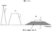
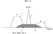
携帯電話端末においては、ゼロIF方式、低IF方式などを用いても、全二重送受信装置は送信と受信が同時に行われるため、特に、マルチバンド化になるほど、高いレベルの送信信号をRFICのみで抑圧するのは困難である。高いレベルの送信信号が存在すると受信信号は図3(a)〜(c)のような妨害成分により受信感度が劣化する。図3(a)〜(c)は携帯電話で多く用いられる周波数配置で送信信号は受信信号より低い周波数帯に割り当てられている例である。 In mobile phone terminals, even if the zero-IF method, low-IF method, etc. are used, full-duplex transmission / reception devices perform transmission and reception at the same time. It is difficult to suppress. When there is a high level transmission signal, the reception sensitivity of the reception signal is deteriorated due to the interference components as shown in FIGS. FIGS. 3A to 3C show an example in which a transmission signal is assigned to a frequency band lower than that of a reception signal in a frequency arrangement often used in a mobile phone.
図3(a)において、1は送信信号、2は受信信号、3は妨害信号、4は受信チャネルに生じる送信信号1と妨害信号3による相互変調妨害である。妨害信号3は送信信号1と受信信号2のほぼ中間の周波数帯に存在する。ここでは、送信信号1と受信信号2は変調された信号(以下、被変調波と記す)であり、妨害信号3は変調されていない信号(以下、CWと記す)であるものとする。従って、送信信号1と受信信号2はある帯域幅をもち、妨害信号3は線スペクトラムとして図示している。 In FIG. 3A, 1 is a transmission signal, 2 is a reception signal, 3 is an interference signal, and 4 is an intermodulation interference caused by the
送信信号1の周波数をftx、妨害信号3の周波数をfjamとすると、受信チャネルに生じる送信信号1と妨害信号3による相互変調妨害4の周波数fiは、式(1)となる。
fi=2fjam-ftx (1)
相互変調妨害は図3(b)のような場合にも生ずる。図3(b)において図3(a)と同様の信号は図3(a)と同じ番号を付し説明を略す。この場合、fiは、式(2)となる。
fi=2ftx-fjam (2)
図3(b)の場合、受信チャネルに生じる送信信号1と妨害信号3による相互変調妨害4は図3(a)の同信号の2倍の帯域幅を有する。When the frequency of the
fi = 2fjam-ftx (1)
Intermodulation interference also occurs in the case shown in FIG. In FIG. 3 (b), the same signals as those in FIG. 3 (a) are given the same numbers as in FIG. In this case, fi is given by equation (2).
fi = 2ftx-fjam (2)
In the case of FIG. 3B, the
妨害信号が受信帯に近接している場合、図3(c)のように混変調歪の影響を受ける。図3(c)において図3(a)と同様の信号は図3(a)と同じ番号を付し説明を略す。5は受信チャネルに生じる送信信号1と妨害信号3による混変調妨害である。混変調歪により、送信信号1に対し2倍の帯域幅の混変調妨害5がfjamを中心周波数として生ずる。これが受信チャネルに混入するため受信感度が劣化する。 When the interference signal is close to the reception band, it is affected by the cross modulation distortion as shown in FIG. In FIG. 3 (c), the same signals as in FIG. 3 (a) are given the same numbers as in FIG.
図3(a)〜(c)による受信感度劣化は送信信号をフィルタで抑圧することで軽減できるので、一般に図4のような構成がとられる。
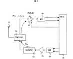
図4において、10はアンテナ、20はデュプレクサ、30はLNA、40はBPF、50はRFIC、60はBPF、70はPA、80はアイソレータである。アンテナ10から入力された無線信号はデュプレクサ20により所望の帯域以外の信号を抑圧し、LNA30に入力される。LNA30はデュプレクサ20の出力信号をできるだけ信号対雑音比(以下、SNRと記す)を劣化させないように増幅する。LNA30の出力信号はBPF40に入力される。BPF40は所望の帯域以外の信号を抑圧し、RFIC50へ入力する。
RFIC50は、ゼロIF方式、低IF方式などの受信方式にて無線信号を処理する。また、RFIC50はLNA30の利得やバイアス電流を切り替える信号を出力し、受信レベルに応じて利得やバイアス電流を切り替える。Since the reception sensitivity degradation due to FIGS. 3A to 3C can be reduced by suppressing the transmission signal with a filter, the configuration as shown in FIG. 4 is generally adopted.
In FIG. 4, 10 is an antenna, 20 is a duplexer, 30 is an LNA, 40 is a BPF, 50 is an RFIC, 60 is a BPF, 70 is a PA, and 80 is an isolator. The radio signal input from the
The
RFIC50は全二重送受信装置向けのため、受信と同時に送信を行う。RFIC50から出力された送信信号はBPF60により所望の帯域以外の信号を抑圧し、PA70へ入力する。PA70は所望のレベルに送信信号を増幅するし、アイソレータ80へ入力する。アイソレータ80はアンテナ10のインピーダンスの変動を受けても効率よくPA70が電力増幅できるよう付与されるものである。
アンテナ10のインピーダンス変動は、例えば、携帯電話のアンテナを頭部に触れて使用した場合などに起こる。Since the
The impedance fluctuation of the
アイソレータ80の出力はデュプレクサ20を経て、アンテナ10より出力される。
このとき、デュプレクサ20は、受信側(LNA30の入力)から見た場合、送信信号を抑圧する効果があり(受信帯以外は全て抑圧する)、送信側(アイソレータ80の出力)から見た場合、受信側からスプリアスなどを抑圧する効果がある(送信帯以外は全て抑圧する)。これにより、図3(a)〜(c)の妨害を軽減する。The output of the
At this time, the
図4においてマルチバンド化するとBPF40の集積化は困難なため、LNA30からBPF40への出力端子、BPF40からRFIC50への入力ピンがバンド数分必要となるため、ピン数が増大し、RFIC50のパッケージサイズが増大する。従って、実装面積が大きくなる。 In FIG. 4, since it is difficult to integrate the
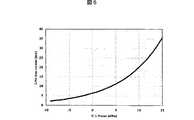
また、LNA30の消費電流はデュプレクサ20の送信信号抑圧度Ltxrx[dB]に依存する。図4のアイソレータ80の出力における送信信号レベルをPtx[dBm]、LNA30の電力利得をPG_LNA[dB]、デュプレクサ20の各ポートインピーダンス、LNA30の入出力インピーダンス、アイソレータ80の出力インピーダンス、BPF40の入力インピーダンスを全て50Ωとする。このとき、BPF40の入力レベルP_LNAout[dBm]は、式(3)となる。
P_LNAout=Ptx-Ltxrx+PG_LNA (3)
P_LNAoutとLNA30のバイアス電流の関係を図5に示す。ここで、P_LNAoutは送信信号の受信側へのリークレベルにより決まるため、Ltxrxに依存する。これを図6に示す。The current consumption of the LNA 30 depends on the transmission signal suppression degree Ltxrx [dB] of the
P_LNAout = Ptx-Ltxrx + PG_LNA (3)
The relationship between the P_LNAout and the bias current of the
図6よりLNA30のバイアス電流はデュプレクサ20の送信信号抑圧度Ltxrxと関係することがわかる。そのため、LNA30をRFIC50に内蔵するには、Ltxrxが何dBあるかによってLNA30のバイアス電流を決めなければならない。しかし、Ltxrxを決めてしまうとRFIC50とデュプレクサ20をセットソリューションとして販売しなければならず、一方、どのようなLtxrxでも利用いただけるようRFIC50を設計しようとすると広範囲にLNA30のバイアス電流を可変できるようにしなければならない。しかし、LNA30は広範囲なバイアス電流で一定の利得となるよう設計するのは現在の技術では非常に困難である。また、LNA30が全バイアス電流で安定であるよう設計するのも難しい。 6 that the bias current of the
従って、RFIC50とLNA30を分離し、デュプレクサ20を選定する設計者がLNA30も設計するのが望ましいが、多バンド化すると実装面積の観点からLNA30をバンド数分集積したLNAICを利用せざるを得ない。しかし、一般にLNAICの設計者もRFIC50の設計者と同様、デュプレクサの選定者と異なるため、やはりLtxrxに依存しない設計をする困難が生ずる。 Therefore, it is desirable that the designer who selects the
上記課題を解決するために、本発明による送受信装置に適用できるモジュールは、アンテナと、該アンテナから、あるいは該アンテナへの信号より所望帯域のみ通過させるデュプレクサと、該デュプレクサの出力信号を増幅する低雑音増幅回路と、該低雑音増幅回路の出力信号より所望帯域のみ通過させる第一の帯域通過フィルタと、該第一の帯域通過フィルタの出力信号を低い周波数帯へ周波数変換する無線信号処理半導体回路と、該無線信号処理半導体回路からの送信信号より所望帯域のみ通過させる第二の帯域通過フィルタと、該第二の帯域通過フィルタの出力信号を増幅する電力増幅回路と、前記アンテナのインピーダンスが変化しても前記電力増幅器が効率よく電力増幅できるよう、前記電力増幅器から前記アンテナを見たインピーダンスが安定するように挿入するアイソレータとを具備し、前記デュプレクサが、前記アイソレータの出力信号より所望帯域のみ通過させ、前記アンテナへ出力する送受信装置に適用できるように構成し、前記デュプレクサと前記低雑音増幅回路と前記第一の帯域通過フィルタが一つのモジュール内にあるように構成することで、全二重送受信装置向け無線信号処理半導体回路の設計容易化、小型化、低消費電力化を図っている。 In order to solve the above-described problems, a module applicable to the transmission / reception apparatus according to the present invention includes an antenna, a duplexer that allows only a desired band to pass from the signal to or from the antenna, and a low-amplifier that amplifies the output signal of the duplexer. A noise amplification circuit, a first band pass filter that passes only a desired band from an output signal of the low noise amplification circuit, and a radio signal processing semiconductor circuit that converts the output signal of the first band pass filter to a lower frequency band A second band-pass filter that passes only a desired band from a transmission signal from the radio signal processing semiconductor circuit, a power amplifier circuit that amplifies an output signal of the second band-pass filter, and an impedance of the antenna changes Even if the power amplifier can amplify the power efficiently, the impedance of the antenna viewed from the power amplifier An isolator that is inserted so that the dance is stable, and the duplexer is configured to be applicable to a transmission / reception device that passes only a desired band from the output signal of the isolator and outputs the signal to the antenna. By configuring the noise amplification circuit and the first bandpass filter to be in one module, the design of the wireless signal processing semiconductor circuit for a full-duplex transmission / reception device is facilitated, reduced in size, and reduced in power consumption. ing.
また、本発明によるモジュールは、前記アイソレータの出力信号を分岐するカップラと、該カップラ出力の信号レベルを検波する検波回路とを具備し、前記検波回路の出力レベルが大きいとき前記低雑音増幅回路のバイアス電流を増加させ、前記検波回路の出力レベルが小さいとき前記低雑音増幅回路のバイアス電流を減少させるように構成することで、送受信装置の低消費電力化を図っている。 The module according to the present invention further includes a coupler that branches the output signal of the isolator, and a detection circuit that detects a signal level of the coupler output. When the output level of the detection circuit is high, the module of the low noise amplification circuit is provided. By increasing the bias current and reducing the bias current of the low-noise amplifier circuit when the output level of the detection circuit is small, the power consumption of the transmission / reception apparatus is reduced.
また、本発明によるモジュールは、前記送受信装置のデュプレクサと、低雑音増幅回路と、第一の帯域通過フィルタと、カップラと、検波回路が一つのモジュール内に構成した送受信装置向けのモジュール部品とすることで、全二重送受信装置向け無線信号処理半導体回路の設計容易化、小型化、低消費電力化を図っている。
さらに、複数の送受信帯に対応してデュプレクサ、低雑音増幅回路、第一の帯域通過フィルタ、無線信号処理半導体回路、第二の帯域通過フィルタ、カップラ、検波回路を複数個モジュール内に構成することで、全二重送受信装置向け無線信号処理半導体回路の設計容易化、小型化、低消費電力化を図っている。
加えて、複数の低雑音増幅回路を対応する帯域向けのみONするための制御信号を、モジュール外部のRFICより供給することにより、全二重送受信装置向け無線信号処理半導体回路の更なる設計容易化、小型化、低消費電力化を図っている。The module according to the present invention is a module component for a transmission / reception device in which the duplexer of the transmission / reception device, a low-noise amplification circuit, a first bandpass filter, a coupler, and a detection circuit are configured in one module. This facilitates design, miniaturization, and low power consumption of the radio signal processing semiconductor circuit for full-duplex transmission / reception devices.
Furthermore, a plurality of duplexers, low-noise amplifier circuits, first band-pass filters, radio signal processing semiconductor circuits, second band-pass filters, couplers, and detection circuits are configured in a plurality of modules corresponding to a plurality of transmission / reception bands. Therefore, the design of a radio signal processing semiconductor circuit for a full-duplex transmission / reception device is facilitated, reduced in size, and reduced in power consumption.
In addition, by supplying a control signal for turning on a plurality of low-noise amplifier circuits only for the corresponding band from the RFIC outside the module, further simplification of the design of the radio signal processing semiconductor circuit for the full-duplex transceiver device , Miniaturization and low power consumption.
実装面においては、本発明による送受信装置向けのモジュールは、複数の送受信信号を切り替えるスイッチと、該スイッチに接続され各送受信信号の周波数分離を行う複数のデュプレクサと、該デュプレクサの受信信号出力信号を増幅する複数の低雑音増幅器と、該低雑音増幅器に接続される複数の帯域通過フィルタとを具備し、帯域通過フィルタが平衡信号を出力することにより、小型化、低歪特性の実現を図っている。また、平衡信号出力端子をモジュール外部に接続するダイレクトコンバージョンミクサ回路の入力端子と対向配置とすることにより、小型化、低歪特性の実現を図っている。さらに、デュプレクサと低雑音増幅器と帯域通過フィルタを複数の受信帯域毎にモノリシック化することにより、さらなる小型化と性能安定化を図っている。加えて、スイッチとデュプレクサと低雑音増幅器と帯域通過フィルタを全てモノリシック化することにより、より一層の小型化を図っている。 In terms of mounting, a module for a transmission / reception device according to the present invention includes a switch that switches a plurality of transmission / reception signals, a plurality of duplexers that are connected to the switch and perform frequency separation of each transmission / reception signal, and a reception signal output signal of the duplexer. A plurality of low-noise amplifiers to be amplified and a plurality of band-pass filters connected to the low-noise amplifiers, and the band-pass filter outputs a balanced signal to achieve downsizing and low distortion characteristics. Yes. Further, the balanced signal output terminal is arranged opposite to the input terminal of the direct conversion mixer circuit that connects to the outside of the module, thereby realizing miniaturization and low distortion characteristics. Further, the duplexer, the low noise amplifier, and the band pass filter are monolithic for each of a plurality of reception bands, thereby further reducing the size and stabilizing the performance. In addition, all the switches, duplexers, low-noise amplifiers, and band-pass filters are monolithically designed to further reduce the size.
本発明により、全二重送受信装置向け無線信号処理半導体回路の設計容易化、小型化、低消費電力化を図ることができる。 According to the present invention, the radio signal processing semiconductor circuit for a full-duplex transmitter / receiver can be easily designed, reduced in size, and reduced in power consumption.
以下、本発明の実施の形態を図面を用いて説明する。 Hereinafter, embodiments of the present invention will be described with reference to the drawings.
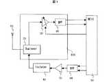
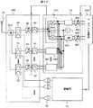
図1は本発明による送受信装置の実施例1を示すブロック図である。図1において、10はアンテナ、20はデュプレクサ、30はLNA、40はBPF、50はRFIC、60はBPF、70はPA、80はアイソレータ、100は高周波フロントエンドモジュールである。アンテナ10から入力された無線信号はデュプレクサ20により所望の帯域以外の信号を抑圧し、LNA30に入力される。LNA30はデュプレクサ20の出力信号をできるだけ信号対雑音比(以下、SNRと記す)を劣化させないように増幅する。LNA30の出力信号はBPF40に入力される。BPF40は所望の帯域以外の信号を抑圧し、RFIC50へ入力する。 FIG. 1 is a block
RFIC50は、ゼロIF方式、低IF方式などの受信方式にて無線信号を処理する。また、RFIC50はLNA30の利得やバイアス電流を切り替える信号を出力し、受信レベルに応じて利得やバイアス電流を切り替える。
RFIC50は全二重送受信装置向けのため、受信と同時に送信を行う。RFIC50から出力された送信信号はBPF60により所望の帯域以外の信号を抑圧し、PA70へ入力する。PA70は所望のレベルに送信信号を増幅し、アイソレータ80へ入力する。アイソレータ80はアンテナ10のインピーダンスの変動を受けても効率よくPA70が電力増幅できるよう付与されるものである。
アンテナ10のインピーダンス変動は、例えば、携帯電話のアンテナを頭部に触れて使用した場合などに起こる。The
Since the
The impedance fluctuation of the
アイソレータ80の出力はデュプレクサ20を経て、アンテナ10より出力される。
このとき、デュプレクサ20は、受信側(LNA30の入力)から見た場合、送信信号を抑圧する効果があり(受信帯以外は全て抑圧する)、送信側(アイソレータ80の出力)から見た場合、受信側からスプリアスなどを抑圧する効果がある(送信帯以外は全て抑圧する)。これにより、図3(a)〜(c)の妨害を軽減する。The output of the
At this time, the
高周波フロントエンドモジュール100は、デュプレクサ20、LNA30、BPF40を1モジュール化したものである。また、図示しないが多バンド化するにはアンテナスイッチをアンテナ10とデュプレクサ20の中間に配し、バンド間の信号切り替えを行う。更に各バンド所望のLNA30の電源ON/OFFの切り替えも行う。アンテナスイッチ、LNA30のバンド間切り替え信号はRFIC50より送られる。 The high-frequency front-
高周波フロントエンドモジュール100により、高周波フロントエンドモジュール100の設計者がLNA30のバイアス電流の最適設計に関与することとなるため、LNA30の利得を設計値に設定したり、安定化したりするのが容易となる。一方、RFIC50は、デュプレクサ20、BPF40により送信信号の受信側へのリークは十分に抑圧されるため、特に送信信号の受信側へのリークレベルを設計時に気にする必要はない。また、高周波フロントエンドモジュール100にLNA30が内蔵されるため、RFIC50の低雑音性要求は低くなり、例えばコストの安いCMOSプロセスで製造できるようになる。 Since the designer of the high-frequency front-
FBAR、BAWフィルタ技術などを用いれば、LNA30を製造するシリコン基板上へデュプレクサ20、BPF40を内蔵することができ、高周波フロントエンドモジュール100をデュプレクサICとすることも可能である。 If FBAR, BAW filter technology, or the like is used, the
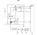
図2は本発明による送受信装置の実施例2を示すブロック図である。図2において、図1と同様の動作を行う部分には図1と同じ番号を付し説明を略す。図2において、110はカップラ、120はパワーディテクタである。LNA30は送信信号の受信側へのリークレベルが小さければ、バイアス電流を小さくし、低消費電力化できる。従って、アイソレータ80の出力信号をカップラ110で分岐し、パワーディテクタ120で送信信号レベルを検波する。パワーディテクタ120で検波した検波レベルに応じてLNA30のバイアス電流を制御する。パワーディテクタ120はショットキーダイオードなど閾値電圧が低く、かつ電力を消費しないタイプのものを用いればより低消費電力化を図ることができる。 FIG. 2 is a block
一方、ショットキーダイオードを用いることのできるプロセスでRFIC50を製造することは稀であるため、パワーディテクタ120をRFIC50へ内蔵すためには、増幅回路を併用したパワーディテクタ120とせざるを得ないので、低消費電力化には向かない。
本発明により、全二重送受信装置向けRFIC50の設計容易化、小型化、低消費電力化を図ることができる。On the other hand, since it is rare to manufacture the
According to the present invention, it is possible to easily design, reduce the size, and reduce the power consumption of the
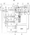
図7は本発明による送受信装置の実施例3を示すブロック図である。本実施例では、マルチバンドに対応した構成の一例を示す。複数の送受信帯域を切り替える高周波スイッチ101に接続されたデュプレクサ202、203、204により全二重通信が可能になっている。各デュプレクサの受信出力には、低雑音増幅器(LNA)が接続され、その後段にはバンドパスフィルタ(BPF)40、41、42が各々接続される。バンドパスフィルタを挿入することにより、受信回路全体の歪特性が向上するとともに、消費電流の削減が可能になる。ここで、BPFは平衡出力を有しており、ダイレクトコンバージョンミクサ501、502、503との接続に都合が良い。これは、外来雑音が混入した場合に、ミクサの同相除去比によって抑圧が期待できるからである。ダイレクトコンバージョンミクサには局部発信器508が接続され、受信希望波の中心周波数と同一の発振周波数を発生することにより、受信希望波をベースバンド帯に周波数変換する。ベースバンド帯に変換された受信信号はチャネル選択のためのLPF504、505を介し可変利得増幅器506、507に接続される。可変利得増幅器によって所望の信号振幅に調整された受信信号は、ベースバンド処理部200に入力され、復調・デコード処理される。
送信側は、ベースバンドからの変調信号を送信部52で所望の高周波変調信号に変換し、電力増幅器70でアンテナ送出に必要な電力レベルに増幅した後、デュプレクサの送信入力に入力される。FIG. 7 is a block
On the transmission side, the modulation signal from the baseband is converted into a desired high-frequency modulation signal by the
本実施例では、各受信帯域毎にデュプレクサ、LNA、BPFを設け、これらを切り替える高周波スイッチに接続し、これらをモジュール化することにより、マルチバンド化した場合においても歪特性向上と消費電流低減が出来る。また、LNAの性能に関与する入出力負荷として接続されるデュプレクサおよびBPFを近接配置できることにより、整合条件の最適化を行い易くなるという利点がある。また、BPFの出力を平衡とすることにより、モジュール外部に接続されるダイレクトコンバージョンミクサ501との接続に都合が良く、また外来雑音に対しての抑圧が期待できる。また、LNAとダイレクトコンバージョンミクサを別にすることで、各々最適な半導体プロセスを選択でき、設計の自由度が増すとともに、性能向上を図ることが出来るという利点がある。
なお、本実施例においてRFIC50をダイレクトコンバージョンレシーバ51と送信部52に分けて示しているが、これらが1チップ化されていても本発明の効果は有効である。In this embodiment, a duplexer, LNA, and BPF are provided for each reception band, connected to a high-frequency switch for switching them, and modularized so that distortion characteristics can be improved and current consumption can be reduced even in a multiband configuration. I can do it. In addition, since the duplexer and the BPF connected as input / output loads related to the performance of the LNA can be arranged close to each other, there is an advantage that the matching condition can be easily optimized. Further, by balancing the output of the BPF, it is convenient for connection to the
In the present embodiment, the
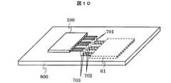
図8は本発明による送受信装置の実施例4を示す構造図である。本実施例では、マルチバンドに対応した場合の実装形態の一例を示す。実装基板800に高周波フロントエンドモジュール100とダイレクトコンバージョンレシーバ51を実装する場合、各々の端子が対向配置となるようにする。これにより、同一面で高周波フロントエンドモジュールとダイレクトコンバージョンレシーバを実装する際、高周波信号線701、702、703が交差することなく短距離で結線できる。これら高周波信号線には平衡信号が通るため、線路の遅延特性や損失特性にインバランスが発生すると受信特性の劣化につながり好ましくない。本実施例の構成により、これを解決することができる。 FIG. 8 is a structural
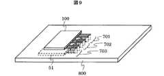
図9は本発明による送受信装置の実施例5を示す構造図である。本実施例も、マルチバンドに対応した場合の実装形態の一例である。実装基板800に高周波フロントエンドモジュール100とダイレクトコンバージョンレシーバ51を各々反対の面に実装する場合を考える。このとき、各々の端子を図9に示す如く透視図上で対向配置となるようにする。これにより、両面実装を行う場合、高周波信号線701、702、703が交差することなく短距離で結線できる。また、各実装面の高周波信号線どうしをviaで接続しているが、viaは寄生インダクタンス成分を有するため、その配置によって信号遅延や振幅のインバランス要因となるため好ましくない。本実施例によれば、配線レイアウトを簡略できるためレイアウトの自由度が増し、平衡信号に対する寄生インダクタンス成分の影響を抑圧することができる。 FIG. 9 is a structural
図10は本発明による送受信装置の実施例6を示す構造図である。本実施例も、マルチバンドに対応した場合の実装形態の一例である。実装基板800に高周波フロントエンドモジュール100とダイレクトコンバージョンレシーバ51を各々反対の面に実装する場合を考える。このとき、他の部品実装との関係で、各々の端子を図10に示す如く透視図上で対向配置となるようにする。これにより、両面実装を行う場合、高周波信号線701、702、703が交差することなく短距離で結線できる。また、各実装面の高周波信号線どうしをviaで接続しているが、viaは寄生インダクタンス成分を有するため、その配置によって信号遅延や振幅のインバランス要因となるため好ましくない。本実施例によれば、配線レイアウトを簡略できるためレイアウトの自由度が増し、平衡信号に対する寄生インダクタンス成分の影響を抑圧することができる。 FIG. 10 is a structural diagram showing Embodiment 6 of the transmitting / receiving apparatus according to the present invention. This embodiment is also an example of a mounting form in the case of supporting multiband. Consider a case where the high-frequency front-
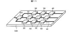
図11は本発明による送受信装置の実施例7を示す構造図である。本実施例では、マルチバンドに対応した高周波フロントエンドモジュールの内部構成の一例を示す。スイッチ101、デュプレクサ20、21、22、LNA30、31、32、そしてBPF40、41、42をモジュール内において別チップで構成する。各構成要素を分離することにより、受信歪特性に関係する送信信号の漏洩を抑圧する効果が期待できる。また、複数の受信帯域毎に性能向上をする場合、再設計を部分的に行い、該当箇所のみの部品交換すること対応できるため設計の自由度と開発期間の短縮を図ることが出来る。 FIG. 11 is a structural
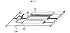
図12は本発明による送受信装置の実施例8を示す構造図である。本実施例も、マルチバンドに対応した高周波フロントエンドモジュールの内部構成の一例を示す。デュプレクサとLNA、BPFを複数の受信帯域毎にモノリシック化する。例えば、デュプレクサおよびBPFを、半導体プロセスで製造可能なBAR(Bulk Acoustic Resonator)で構成すれば、モノリシック化が可能である。この場合、製造コストの削減を図ることができるとともに、モノリシック化による性能安定化、各チップのパッケージング数削減による小型化・低コスト化を図ることができる。なお、モノリシック化する範囲は、一つあるいはいくつかの受信帯に限って部分的に実施しても、同様の効果が得られる。また、高周波スイッチ101を含めて、高周波フロントエンドモジュール全てをモノリシック化しても、さらなるコスト削減が期待できる。 FIG. 12 is a structural diagram showing Embodiment 8 of the transmitting / receiving apparatus according to the present invention. This embodiment also shows an example of the internal configuration of a high-frequency front-end module that supports multiband. The duplexer, LNA, and BPF are monolithic for each of a plurality of reception bands. For example, if the duplexer and the BPF are configured by a BAR (Bulk Acoustic Resonator) that can be manufactured by a semiconductor process, monolithic can be realized. In this case, the manufacturing cost can be reduced, the performance can be stabilized by monolithic, and the size and cost can be reduced by reducing the number of packaging of each chip. The same effect can be obtained even if the monolithic range is partially implemented only for one or several reception bands. Further, even if all the high-frequency front end modules including the high-
図13は本発明による送受信装置の実施例9を示すブロック図である。本実施例では、ベースバンド処理部よりLNAの利得制御を行う場合の構成例である。高周波フロントエンドモジュールは、利得制御信号の入力端子を有し、印加される電圧、電流あるいはデータに応じて各LNAの利得や電流値を制御することができる。本実施例によれば、高周波フロントエンドモジュールに具備するLNAの利得や電流値をモジュール外部から制御できるようにすることにより、受信回路全体の性能最適化が容易に実現できるという利点がある。 FIG. 13 is a block diagram showing Embodiment 9 of the transmitting / receiving apparatus according to the present invention. The present embodiment is a configuration example in the case where LNA gain control is performed by the baseband processing unit. The high-frequency front end module has an input terminal for a gain control signal, and can control the gain and current value of each LNA according to the applied voltage, current, or data. According to the present embodiment, there is an advantage that the performance optimization of the entire receiving circuit can be easily realized by enabling the gain and current value of the LNA included in the high-frequency front-end module to be controlled from the outside of the module.
図14は本発明による送受信装置の実施例10を示すブロック図である。本実施例では、RFIC(ダイレクトコンバージョンレシーバ51)よりLNAの利得制御を行う場合の構成例である。高周波フロントエンドモジュールは、利得制御信号の入力端子を有し、印加される電圧、電流あるいはデータに応じて各LNAの利得や電流値を制御することができる。本実施例によれば、高周波フロントエンドモジュールに具備するLNAの利得や電流値をモジュール外部から制御できるようにすることにより、受信回路全体の性能最適化が容易に実現できるという利点がある。また、これを用いた送受信装置装置においては、ベースバンド処理部の負荷を軽減できるという利点がある。これは、元々ベースバンド処理部からRFICに対して可変利得増幅器の利得制御や局部発振器の周波数設定等の目的で制御が行われているので、RFIC側に制御信号を発生する手段(図示せず)を設ければ、新たにベースバンド処理部から制御信号を発生することなく(処理を増加することなく)、高周波フロントエンドモジュールに具備するLNAの利得や電流値をモジュール外部から制御することができる。 FIG. 14 is a block
CDMA方式携帯電話およびこれに用いる高周波フロントエンドモジュールとして適用できる。 It can be applied as a CDMA mobile phone and a high-frequency front-end module used therefor.
1… 送信信号
2… 受信信号
3… 妨害信号
4… 受信チャネルに生じる送信信号1と妨害信号3による相互変調妨害
5… 受信チャネルに生じる送信信号1と妨害信号3による混変調妨害
10… アンテナ
20、202、203、204… デュプレクサ
30、31、32… 低雑音増幅器(LNA)
40、41、42、60… バンドパスフィルタ(BPF)
50… RFIC
51… ダイレクトコンバージョンレシーバ
52… 送信部
70… 電力増幅器(PA)
80… アイソレータ
100… 高周波フロントエンドモジュール
101… 高周波スイッチ
110… カップラ
120… パワーディテクタ
501、502、503… ダイレクトコンバージョンミクサ
504、505… ローパスフィルタ(LPF)
506、507… 可変利得増幅器
508… 局部発信器
701、702、703… 高周波信号線
DESCRIPTION OF
40, 41, 42, 60 ... Band pass filter (BPF)
50 ... RFIC
51 ...
DESCRIPTION OF
506, 507 ...
Claims (13)
Translated fromJapanese前記デュプレクサと前記低雑音増幅回路と前記第一の帯域通過フィルタが一つのモジュール内に構成されていることを特徴としたモジュール。An antenna, a duplexer that passes only a desired band from the signal to or from the antenna, a low-noise amplifier circuit that amplifies the output signal of the duplexer, and passes only a desired band from the output signal of the low-noise amplifier circuit A first band-pass filter, a radio signal processing semiconductor circuit for frequency-converting the output signal of the first band-pass filter to a lower frequency band, and a first band-pass filter that passes only a desired band from a transmission signal from the radio signal processing semiconductor circuit. A second band-pass filter, a power amplification circuit that amplifies the output signal of the second band-pass filter, and the power amplifier so that the power amplifier can efficiently amplify power even when the impedance of the antenna changes. An isolator that is inserted so that the impedance when the antenna is viewed is stabilized, and the duplexer Only a desired band from an output signal of the isolator is passed through a module that can be applied to transmitting and receiving apparatus for outputting to the antenna,
The module, wherein the duplexer, the low-noise amplifier circuit, and the first band pass filter are configured in one module.
前記検波回路の出力レベルが大きいとき前記低雑音増幅回路のバイアス電流を増加させ、前記検波回路の出力レベルが小さいとき前記低雑音増幅回路のバイアス電流を減少させることを特徴とした送受信装置。An antenna, a duplexer that passes only a desired band from the signal to or from the antenna, a low-noise amplifier circuit that amplifies the output signal of the duplexer, and passes only a desired band from the output signal of the low-noise amplifier circuit A first band-pass filter, a radio signal processing semiconductor circuit for frequency-converting the output signal of the first band-pass filter to a lower frequency band, and a first band-pass filter that passes only a desired band from a transmission signal from the radio signal processing semiconductor circuit. A second band-pass filter, a power amplification circuit that amplifies the output signal of the second band-pass filter, and the power amplifier so that the power amplifier can efficiently amplify power even when the impedance of the antenna changes. An isolator to be inserted so that the impedance viewed from the antenna is stable, and an output signal of the isolator A coupler for branching, comprising a detection circuit for detecting a signal level of the coupler output, the duplexer, passed only a desired band from an output signal of the isolator, a transceiver to be output to the antenna,
A transmission / reception apparatus characterized by increasing the bias current of the low noise amplifier circuit when the output level of the detection circuit is large and decreasing the bias current of the low noise amplifier circuit when the output level of the detection circuit is small.
前記デュプレクサと、前記低雑音増幅回路と、前記第一の帯域通過フィルタと、前記カップラと、前記検波回路が一つのモジュール内に構成され、前記検波回路の出力レベルが大きいとき前記低雑音増幅回路のバイアス電流を増加させ、前記検波回路の出力レベルが小さいとき前記低雑音増幅回路のバイアス電流を減少させることを特徴としたモジュール。An antenna, a duplexer that passes only a desired band from the signal to or from the antenna, a low-noise amplifier circuit that amplifies the output signal of the duplexer, and passes only a desired band from the output signal of the low-noise amplifier circuit A first band-pass filter, a radio signal processing semiconductor circuit for frequency-converting the output signal of the first band-pass filter to a lower frequency band, and a first band-pass filter that passes only a desired band from a transmission signal from the radio signal processing semiconductor circuit. A second band-pass filter, a power amplification circuit that amplifies the output signal of the second band-pass filter, and the power amplifier so that the power amplifier can efficiently amplify power even when the impedance of the antenna changes. An isolator to be inserted so that the impedance viewed from the antenna is stable, and an output signal of the isolator A module that includes a branching coupler and a detection circuit that detects a signal level of the coupler output, and wherein the duplexer passes only a desired band from the output signal of the isolator and is applied to a transmission / reception device that outputs the signal to the antenna. And
The duplexer, the low-noise amplifier circuit, the first band-pass filter, the coupler, and the detection circuit are configured in one module, and the low-noise amplifier circuit when the output level of the detection circuit is large And a bias current of the low-noise amplifier circuit is decreased when the output level of the detection circuit is small.
前記アンテナスイッチと前記デュプレクサと前記低雑音増幅回路と前記第一の帯域通過フィルタと前記カップラと前記検波回路が一つのモジュール内に構成されていることを特徴としたモジュール。From an antenna corresponding to operation in N transmission / reception bands, an antenna switch for switching signals of N transmission / reception bands to / from the antenna, and signals from the antenna switch or to the antenna switch N duplexers that pass only the desired band, N low-noise amplifier circuits for N reception bands that amplify the output signal of the duplexer, and N receptions that pass only the desired band from the output signal of the low-noise amplifier circuit N first bandpass filters for the band, a radio signal processing semiconductor circuit that converts the output signal of the first bandpass filter to a lower frequency band, and a desired band from a transmission signal from the radio signal processing semiconductor circuit N band-pass filters for N transmission bands that only pass through and the output signal of the second band-pass filter at the desired transmission level N power amplifier circuits for N transmission bands that are amplified so that they can be output from a tenor, and the antenna is viewed from the power amplifier so that the power amplifier can efficiently amplify power even if the impedance of the antenna changes. N transmission band isolators inserted so as to stabilize the impedance, N transmission band couplers that branch the output signal of the isolator, and the signal level of the coupler output are detected, and the detection is performed. N transmission band detection circuits for increasing the bias current of the low noise amplification circuit when the output level is high and decreasing the bias current of the low noise amplification circuit when the detection output level is small, The duplexer is a module that can be applied to a transmission / reception device that passes only a desired band from an output signal of the isolator and outputs the signal to the antenna,
The module, wherein the antenna switch, the duplexer, the low noise amplification circuit, the first band pass filter, the coupler, and the detection circuit are configured in one module.
前記帯域通過フィルタが平衡信号を出力することを特徴とする送受信装置向けのモジュール。A switch for switching a plurality of transmission / reception signals, a plurality of duplexers connected to the switch for frequency separation of the transmission / reception signals, a plurality of low noise amplifiers for amplifying the reception signal output signals of the duplexers, and a connection to the low noise amplifier A plurality of bandpass filters to be provided,
A module for a transmission / reception device, wherein the band-pass filter outputs a balanced signal.
13. The transmission / reception device according to claim 12, wherein when the module for the transmission / reception device and the direct conversion reception circuit are mounted on the same surface, the signal line of the balanced signal output from the module is the direct conversion reception. A transmission / reception device connected to a circuit in an opposing arrangement.
Priority Applications (3)
| Application Number | Priority Date | Filing Date | Title |
|---|---|---|---|
| JP2004357538AJP2006166277A (en) | 2004-12-10 | 2004-12-10 | Transceiver and module |
| DE102005058459ADE102005058459A1 (en) | 2004-12-10 | 2005-12-07 | Transceiver device and module |
| US11/297,318US20060128322A1 (en) | 2004-12-10 | 2005-12-09 | Transceiver apparatus and module |
Applications Claiming Priority (1)
| Application Number | Priority Date | Filing Date | Title |
|---|---|---|---|
| JP2004357538AJP2006166277A (en) | 2004-12-10 | 2004-12-10 | Transceiver and module |
Publications (1)
| Publication Number | Publication Date |
|---|---|
| JP2006166277Atrue JP2006166277A (en) | 2006-06-22 |
Family
ID=36580349
Family Applications (1)
| Application Number | Title | Priority Date | Filing Date |
|---|---|---|---|
| JP2004357538APendingJP2006166277A (en) | 2004-12-10 | 2004-12-10 | Transceiver and module |
Country Status (3)
| Country | Link |
|---|---|
| US (1) | US20060128322A1 (en) |
| JP (1) | JP2006166277A (en) |
| DE (1) | DE102005058459A1 (en) |
Cited By (8)
| Publication number | Priority date | Publication date | Assignee | Title |
|---|---|---|---|---|
| JP2009094713A (en)* | 2007-10-05 | 2009-04-30 | Hitachi Media Electoronics Co Ltd | Module and mobile communication terminal using the same |
| JP2016042696A (en)* | 2014-08-13 | 2016-03-31 | スカイワークス ソリューションズ, インコーポレイテッドSkyworks Solutions, Inc. | Carrier aggregation (ca) architecture, radio-frequency (rf) module, and radio-frequency (rf) device |
| JP2016092830A (en)* | 2014-10-31 | 2016-05-23 | スカイワークス ソリューションズ, インコーポレイテッドSkyworks Solutions, Inc. | Diversity receiver front-end system with amplifier post-filter |
| KR20200119853A (en)* | 2018-03-23 | 2020-10-20 | 가부시키가이샤 무라타 세이사쿠쇼 | High frequency module and communication device |
| KR20200122358A (en)* | 2018-03-23 | 2020-10-27 | 가부시키가이샤 무라타 세이사쿠쇼 | High frequency module and communication device |
| WO2021039083A1 (en)* | 2019-08-28 | 2021-03-04 | 株式会社村田製作所 | High-frequency module and communication device |
| KR20210108314A (en)* | 2020-02-25 | 2021-09-02 | 가부시키가이샤 무라타 세이사쿠쇼 | Radio frequency module and communication device |
| JP7577892B1 (en) | 2024-07-17 | 2024-11-05 | ソフトバンク株式会社 | Interference suppression circuit, transmission/reception circuit, and radio device |
Families Citing this family (185)
| Publication number | Priority date | Publication date | Assignee | Title |
|---|---|---|---|---|
| US9026070B2 (en) | 2003-12-18 | 2015-05-05 | Qualcomm Incorporated | Low-power wireless diversity receiver with multiple receive paths |
| US7389090B1 (en)* | 2004-10-25 | 2008-06-17 | Micro Mobio, Inc. | Diplexer circuit for wireless communication devices |
| US9450665B2 (en) | 2005-10-19 | 2016-09-20 | Qualcomm Incorporated | Diversity receiver for wireless communication |
| DE102007004911A1 (en)* | 2007-01-26 | 2008-08-07 | Funkwerk Dabendorf Gmbh | Multi-part circuit arrangement for damping compensation |
| US9178669B2 (en) | 2011-05-17 | 2015-11-03 | Qualcomm Incorporated | Non-adjacent carrier aggregation architecture |
| US9252827B2 (en) | 2011-06-27 | 2016-02-02 | Qualcomm Incorporated | Signal splitting carrier aggregation receiver architecture |
| US9154179B2 (en) | 2011-06-29 | 2015-10-06 | Qualcomm Incorporated | Receiver with bypass mode for improved sensitivity |
| US12081243B2 (en)* | 2011-08-16 | 2024-09-03 | Qualcomm Incorporated | Low noise amplifiers with combined outputs |
| US9325353B2 (en)* | 2011-09-16 | 2016-04-26 | Rf Micro Devices, Inc. | Architecture for a radio frequency front-end |
| US8774334B2 (en) | 2011-11-09 | 2014-07-08 | Qualcomm Incorporated | Dynamic receiver switching |
| US20130155911A1 (en)* | 2011-12-16 | 2013-06-20 | Broadcom Corporation | Radio Transceiver With IM2 Mitigation |
| US9172402B2 (en) | 2012-03-02 | 2015-10-27 | Qualcomm Incorporated | Multiple-input and multiple-output carrier aggregation receiver reuse architecture |
| US9362958B2 (en) | 2012-03-02 | 2016-06-07 | Qualcomm Incorporated | Single chip signal splitting carrier aggregation receiver architecture |
| US9118439B2 (en) | 2012-04-06 | 2015-08-25 | Qualcomm Incorporated | Receiver for imbalanced carriers |
| TWI462497B (en)* | 2012-05-23 | 2014-11-21 | Wistron Neweb Corp | Rf circuit system and method of improving the isolation thereof |
| US9154356B2 (en) | 2012-05-25 | 2015-10-06 | Qualcomm Incorporated | Low noise amplifiers for carrier aggregation |
| US9867194B2 (en) | 2012-06-12 | 2018-01-09 | Qualcomm Incorporated | Dynamic UE scheduling with shared antenna and carrier aggregation |
| US9300420B2 (en) | 2012-09-11 | 2016-03-29 | Qualcomm Incorporated | Carrier aggregation receiver architecture |
| US9543903B2 (en) | 2012-10-22 | 2017-01-10 | Qualcomm Incorporated | Amplifiers with noise splitting |
| US9113347B2 (en) | 2012-12-05 | 2015-08-18 | At&T Intellectual Property I, Lp | Backhaul link for distributed antenna system |
| US10009065B2 (en) | 2012-12-05 | 2018-06-26 | At&T Intellectual Property I, L.P. | Backhaul link for distributed antenna system |
| US8995591B2 (en) | 2013-03-14 | 2015-03-31 | Qualcomm, Incorporated | Reusing a single-chip carrier aggregation receiver to support non-cellular diversity |
| US9999038B2 (en) | 2013-05-31 | 2018-06-12 | At&T Intellectual Property I, L.P. | Remote distributed antenna system |
| US9525524B2 (en) | 2013-05-31 | 2016-12-20 | At&T Intellectual Property I, L.P. | Remote distributed antenna system |
| US8897697B1 (en) | 2013-11-06 | 2014-11-25 | At&T Intellectual Property I, Lp | Millimeter-wave surface-wave communications |
| US9209902B2 (en) | 2013-12-10 | 2015-12-08 | At&T Intellectual Property I, L.P. | Quasi-optical coupler |
| US9692101B2 (en) | 2014-08-26 | 2017-06-27 | At&T Intellectual Property I, L.P. | Guided wave couplers for coupling electromagnetic waves between a waveguide surface and a surface of a wire |
| US9768833B2 (en) | 2014-09-15 | 2017-09-19 | At&T Intellectual Property I, L.P. | Method and apparatus for sensing a condition in a transmission medium of electromagnetic waves |
| US10063280B2 (en) | 2014-09-17 | 2018-08-28 | At&T Intellectual Property I, L.P. | Monitoring and mitigating conditions in a communication network |
| US9628854B2 (en) | 2014-09-29 | 2017-04-18 | At&T Intellectual Property I, L.P. | Method and apparatus for distributing content in a communication network |
| US9615269B2 (en) | 2014-10-02 | 2017-04-04 | At&T Intellectual Property I, L.P. | Method and apparatus that provides fault tolerance in a communication network |
| US9685992B2 (en) | 2014-10-03 | 2017-06-20 | At&T Intellectual Property I, L.P. | Circuit panel network and methods thereof |
| US9503189B2 (en) | 2014-10-10 | 2016-11-22 | At&T Intellectual Property I, L.P. | Method and apparatus for arranging communication sessions in a communication system |
| US9973299B2 (en) | 2014-10-14 | 2018-05-15 | At&T Intellectual Property I, L.P. | Method and apparatus for adjusting a mode of communication in a communication network |
| US9762289B2 (en) | 2014-10-14 | 2017-09-12 | At&T Intellectual Property I, L.P. | Method and apparatus for transmitting or receiving signals in a transportation system |
| US9577306B2 (en) | 2014-10-21 | 2017-02-21 | At&T Intellectual Property I, L.P. | Guided-wave transmission device and methods for use therewith |
| US9769020B2 (en) | 2014-10-21 | 2017-09-19 | At&T Intellectual Property I, L.P. | Method and apparatus for responding to events affecting communications in a communication network |
| US9312919B1 (en) | 2014-10-21 | 2016-04-12 | At&T Intellectual Property I, Lp | Transmission device with impairment compensation and methods for use therewith |
| US9564947B2 (en) | 2014-10-21 | 2017-02-07 | At&T Intellectual Property I, L.P. | Guided-wave transmission device with diversity and methods for use therewith |
| US9780834B2 (en) | 2014-10-21 | 2017-10-03 | At&T Intellectual Property I, L.P. | Method and apparatus for transmitting electromagnetic waves |
| US9653770B2 (en) | 2014-10-21 | 2017-05-16 | At&T Intellectual Property I, L.P. | Guided wave coupler, coupling module and methods for use therewith |
| US9627768B2 (en) | 2014-10-21 | 2017-04-18 | At&T Intellectual Property I, L.P. | Guided-wave transmission device with non-fundamental mode propagation and methods for use therewith |
| US9520945B2 (en) | 2014-10-21 | 2016-12-13 | At&T Intellectual Property I, L.P. | Apparatus for providing communication services and methods thereof |
| US9742462B2 (en) | 2014-12-04 | 2017-08-22 | At&T Intellectual Property I, L.P. | Transmission medium and communication interfaces and methods for use therewith |
| US9461706B1 (en) | 2015-07-31 | 2016-10-04 | At&T Intellectual Property I, Lp | Method and apparatus for exchanging communication signals |
| US10009067B2 (en) | 2014-12-04 | 2018-06-26 | At&T Intellectual Property I, L.P. | Method and apparatus for configuring a communication interface |
| US10340573B2 (en) | 2016-10-26 | 2019-07-02 | At&T Intellectual Property I, L.P. | Launcher with cylindrical coupling device and methods for use therewith |
| US10243784B2 (en) | 2014-11-20 | 2019-03-26 | At&T Intellectual Property I, L.P. | System for generating topology information and methods thereof |
| US9997819B2 (en) | 2015-06-09 | 2018-06-12 | At&T Intellectual Property I, L.P. | Transmission medium and method for facilitating propagation of electromagnetic waves via a core |
| US9954287B2 (en) | 2014-11-20 | 2018-04-24 | At&T Intellectual Property I, L.P. | Apparatus for converting wireless signals and electromagnetic waves and methods thereof |
| US9654173B2 (en) | 2014-11-20 | 2017-05-16 | At&T Intellectual Property I, L.P. | Apparatus for powering a communication device and methods thereof |
| US9544006B2 (en) | 2014-11-20 | 2017-01-10 | At&T Intellectual Property I, L.P. | Transmission device with mode division multiplexing and methods for use therewith |
| US9800327B2 (en) | 2014-11-20 | 2017-10-24 | At&T Intellectual Property I, L.P. | Apparatus for controlling operations of a communication device and methods thereof |
| US9680670B2 (en) | 2014-11-20 | 2017-06-13 | At&T Intellectual Property I, L.P. | Transmission device with channel equalization and control and methods for use therewith |
| KR102273799B1 (en)* | 2014-12-05 | 2021-07-06 | 삼성전자주식회사 | communication circuit for communication function and electronic device including the same |
| US10144036B2 (en) | 2015-01-30 | 2018-12-04 | At&T Intellectual Property I, L.P. | Method and apparatus for mitigating interference affecting a propagation of electromagnetic waves guided by a transmission medium |
| US9876570B2 (en) | 2015-02-20 | 2018-01-23 | At&T Intellectual Property I, Lp | Guided-wave transmission device with non-fundamental mode propagation and methods for use therewith |
| US9749013B2 (en) | 2015-03-17 | 2017-08-29 | At&T Intellectual Property I, L.P. | Method and apparatus for reducing attenuation of electromagnetic waves guided by a transmission medium |
| US9705561B2 (en) | 2015-04-24 | 2017-07-11 | At&T Intellectual Property I, L.P. | Directional coupling device and methods for use therewith |
| US10224981B2 (en) | 2015-04-24 | 2019-03-05 | At&T Intellectual Property I, Lp | Passive electrical coupling device and methods for use therewith |
| US9948354B2 (en) | 2015-04-28 | 2018-04-17 | At&T Intellectual Property I, L.P. | Magnetic coupling device with reflective plate and methods for use therewith |
| US9793954B2 (en) | 2015-04-28 | 2017-10-17 | At&T Intellectual Property I, L.P. | Magnetic coupling device and methods for use therewith |
| US9871282B2 (en) | 2015-05-14 | 2018-01-16 | At&T Intellectual Property I, L.P. | At least one transmission medium having a dielectric surface that is covered at least in part by a second dielectric |
| US9490869B1 (en) | 2015-05-14 | 2016-11-08 | At&T Intellectual Property I, L.P. | Transmission medium having multiple cores and methods for use therewith |
| US9748626B2 (en) | 2015-05-14 | 2017-08-29 | At&T Intellectual Property I, L.P. | Plurality of cables having different cross-sectional shapes which are bundled together to form a transmission medium |
| US10679767B2 (en) | 2015-05-15 | 2020-06-09 | At&T Intellectual Property I, L.P. | Transmission medium having a conductive material and methods for use therewith |
| US10650940B2 (en) | 2015-05-15 | 2020-05-12 | At&T Intellectual Property I, L.P. | Transmission medium having a conductive material and methods for use therewith |
| US9917341B2 (en) | 2015-05-27 | 2018-03-13 | At&T Intellectual Property I, L.P. | Apparatus and method for launching electromagnetic waves and for modifying radial dimensions of the propagating electromagnetic waves |
| US10103801B2 (en) | 2015-06-03 | 2018-10-16 | At&T Intellectual Property I, L.P. | Host node device and methods for use therewith |
| US10154493B2 (en) | 2015-06-03 | 2018-12-11 | At&T Intellectual Property I, L.P. | Network termination and methods for use therewith |
| US10348391B2 (en) | 2015-06-03 | 2019-07-09 | At&T Intellectual Property I, L.P. | Client node device with frequency conversion and methods for use therewith |
| US10812174B2 (en) | 2015-06-03 | 2020-10-20 | At&T Intellectual Property I, L.P. | Client node device and methods for use therewith |
| US9866309B2 (en) | 2015-06-03 | 2018-01-09 | At&T Intellectual Property I, Lp | Host node device and methods for use therewith |
| US9912381B2 (en) | 2015-06-03 | 2018-03-06 | At&T Intellectual Property I, Lp | Network termination and methods for use therewith |
| US9913139B2 (en) | 2015-06-09 | 2018-03-06 | At&T Intellectual Property I, L.P. | Signal fingerprinting for authentication of communicating devices |
| US10142086B2 (en) | 2015-06-11 | 2018-11-27 | At&T Intellectual Property I, L.P. | Repeater and methods for use therewith |
| US9608692B2 (en) | 2015-06-11 | 2017-03-28 | At&T Intellectual Property I, L.P. | Repeater and methods for use therewith |
| US9820146B2 (en) | 2015-06-12 | 2017-11-14 | At&T Intellectual Property I, L.P. | Method and apparatus for authentication and identity management of communicating devices |
| US9667317B2 (en) | 2015-06-15 | 2017-05-30 | At&T Intellectual Property I, L.P. | Method and apparatus for providing security using network traffic adjustments |
| US9865911B2 (en) | 2015-06-25 | 2018-01-09 | At&T Intellectual Property I, L.P. | Waveguide system for slot radiating first electromagnetic waves that are combined into a non-fundamental wave mode second electromagnetic wave on a transmission medium |
| US9509415B1 (en) | 2015-06-25 | 2016-11-29 | At&T Intellectual Property I, L.P. | Methods and apparatus for inducing a fundamental wave mode on a transmission medium |
| US9640850B2 (en) | 2015-06-25 | 2017-05-02 | At&T Intellectual Property I, L.P. | Methods and apparatus for inducing a non-fundamental wave mode on a transmission medium |
| US10148016B2 (en) | 2015-07-14 | 2018-12-04 | At&T Intellectual Property I, L.P. | Apparatus and methods for communicating utilizing an antenna array |
| US10320586B2 (en) | 2015-07-14 | 2019-06-11 | At&T Intellectual Property I, L.P. | Apparatus and methods for generating non-interfering electromagnetic waves on an insulated transmission medium |
| US10341142B2 (en) | 2015-07-14 | 2019-07-02 | At&T Intellectual Property I, L.P. | Apparatus and methods for generating non-interfering electromagnetic waves on an uninsulated conductor |
| US9628116B2 (en) | 2015-07-14 | 2017-04-18 | At&T Intellectual Property I, L.P. | Apparatus and methods for transmitting wireless signals |
| US9836957B2 (en) | 2015-07-14 | 2017-12-05 | At&T Intellectual Property I, L.P. | Method and apparatus for communicating with premises equipment |
| US9722318B2 (en) | 2015-07-14 | 2017-08-01 | At&T Intellectual Property I, L.P. | Method and apparatus for coupling an antenna to a device |
| US10170840B2 (en) | 2015-07-14 | 2019-01-01 | At&T Intellectual Property I, L.P. | Apparatus and methods for sending or receiving electromagnetic signals |
| US9847566B2 (en) | 2015-07-14 | 2017-12-19 | At&T Intellectual Property I, L.P. | Method and apparatus for adjusting a field of a signal to mitigate interference |
| US9853342B2 (en) | 2015-07-14 | 2017-12-26 | At&T Intellectual Property I, L.P. | Dielectric transmission medium connector and methods for use therewith |
| US10205655B2 (en) | 2015-07-14 | 2019-02-12 | At&T Intellectual Property I, L.P. | Apparatus and methods for communicating utilizing an antenna array and multiple communication paths |
| US10044409B2 (en) | 2015-07-14 | 2018-08-07 | At&T Intellectual Property I, L.P. | Transmission medium and methods for use therewith |
| US9882257B2 (en) | 2015-07-14 | 2018-01-30 | At&T Intellectual Property I, L.P. | Method and apparatus for launching a wave mode that mitigates interference |
| US10033107B2 (en) | 2015-07-14 | 2018-07-24 | At&T Intellectual Property I, L.P. | Method and apparatus for coupling an antenna to a device |
| US10033108B2 (en) | 2015-07-14 | 2018-07-24 | At&T Intellectual Property I, L.P. | Apparatus and methods for generating an electromagnetic wave having a wave mode that mitigates interference |
| US9608740B2 (en) | 2015-07-15 | 2017-03-28 | At&T Intellectual Property I, L.P. | Method and apparatus for launching a wave mode that mitigates interference |
| US9793951B2 (en) | 2015-07-15 | 2017-10-17 | At&T Intellectual Property I, L.P. | Method and apparatus for launching a wave mode that mitigates interference |
| US10090606B2 (en) | 2015-07-15 | 2018-10-02 | At&T Intellectual Property I, L.P. | Antenna system with dielectric array and methods for use therewith |
| US9871283B2 (en) | 2015-07-23 | 2018-01-16 | At&T Intellectual Property I, Lp | Transmission medium having a dielectric core comprised of plural members connected by a ball and socket configuration |
| US9912027B2 (en) | 2015-07-23 | 2018-03-06 | At&T Intellectual Property I, L.P. | Method and apparatus for exchanging communication signals |
| US9948333B2 (en) | 2015-07-23 | 2018-04-17 | At&T Intellectual Property I, L.P. | Method and apparatus for wireless communications to mitigate interference |
| US10784670B2 (en) | 2015-07-23 | 2020-09-22 | At&T Intellectual Property I, L.P. | Antenna support for aligning an antenna |
| US9749053B2 (en) | 2015-07-23 | 2017-08-29 | At&T Intellectual Property I, L.P. | Node device, repeater and methods for use therewith |
| US10020587B2 (en) | 2015-07-31 | 2018-07-10 | At&T Intellectual Property I, L.P. | Radial antenna and methods for use therewith |
| US9967173B2 (en) | 2015-07-31 | 2018-05-08 | At&T Intellectual Property I, L.P. | Method and apparatus for authentication and identity management of communicating devices |
| US9735833B2 (en) | 2015-07-31 | 2017-08-15 | At&T Intellectual Property I, L.P. | Method and apparatus for communications management in a neighborhood network |
| US9904535B2 (en) | 2015-09-14 | 2018-02-27 | At&T Intellectual Property I, L.P. | Method and apparatus for distributing software |
| US10079661B2 (en) | 2015-09-16 | 2018-09-18 | At&T Intellectual Property I, L.P. | Method and apparatus for use with a radio distributed antenna system having a clock reference |
| US10009901B2 (en) | 2015-09-16 | 2018-06-26 | At&T Intellectual Property I, L.P. | Method, apparatus, and computer-readable storage medium for managing utilization of wireless resources between base stations |
| US10136434B2 (en) | 2015-09-16 | 2018-11-20 | At&T Intellectual Property I, L.P. | Method and apparatus for use with a radio distributed antenna system having an ultra-wideband control channel |
| US10009063B2 (en) | 2015-09-16 | 2018-06-26 | At&T Intellectual Property I, L.P. | Method and apparatus for use with a radio distributed antenna system having an out-of-band reference signal |
| US9705571B2 (en) | 2015-09-16 | 2017-07-11 | At&T Intellectual Property I, L.P. | Method and apparatus for use with a radio distributed antenna system |
| US10051629B2 (en) | 2015-09-16 | 2018-08-14 | At&T Intellectual Property I, L.P. | Method and apparatus for use with a radio distributed antenna system having an in-band reference signal |
| US9769128B2 (en) | 2015-09-28 | 2017-09-19 | At&T Intellectual Property I, L.P. | Method and apparatus for encryption of communications over a network |
| US9729197B2 (en) | 2015-10-01 | 2017-08-08 | At&T Intellectual Property I, L.P. | Method and apparatus for communicating network management traffic over a network |
| US9876264B2 (en) | 2015-10-02 | 2018-01-23 | At&T Intellectual Property I, Lp | Communication system, guided wave switch and methods for use therewith |
| US9882277B2 (en) | 2015-10-02 | 2018-01-30 | At&T Intellectual Property I, Lp | Communication device and antenna assembly with actuated gimbal mount |
| US10074890B2 (en) | 2015-10-02 | 2018-09-11 | At&T Intellectual Property I, L.P. | Communication device and antenna with integrated light assembly |
| US10051483B2 (en) | 2015-10-16 | 2018-08-14 | At&T Intellectual Property I, L.P. | Method and apparatus for directing wireless signals |
| US10355367B2 (en) | 2015-10-16 | 2019-07-16 | At&T Intellectual Property I, L.P. | Antenna structure for exchanging wireless signals |
| US10665942B2 (en) | 2015-10-16 | 2020-05-26 | At&T Intellectual Property I, L.P. | Method and apparatus for adjusting wireless communications |
| US10177722B2 (en) | 2016-01-12 | 2019-01-08 | Qualcomm Incorporated | Carrier aggregation low-noise amplifier with tunable integrated power splitter |
| US9912419B1 (en) | 2016-08-24 | 2018-03-06 | At&T Intellectual Property I, L.P. | Method and apparatus for managing a fault in a distributed antenna system |
| US9860075B1 (en) | 2016-08-26 | 2018-01-02 | At&T Intellectual Property I, L.P. | Method and communication node for broadband distribution |
| US10291311B2 (en) | 2016-09-09 | 2019-05-14 | At&T Intellectual Property I, L.P. | Method and apparatus for mitigating a fault in a distributed antenna system |
| US11032819B2 (en) | 2016-09-15 | 2021-06-08 | At&T Intellectual Property I, L.P. | Method and apparatus for use with a radio distributed antenna system having a control channel reference signal |
| US10340600B2 (en) | 2016-10-18 | 2019-07-02 | At&T Intellectual Property I, L.P. | Apparatus and methods for launching guided waves via plural waveguide systems |
| US10135147B2 (en) | 2016-10-18 | 2018-11-20 | At&T Intellectual Property I, L.P. | Apparatus and methods for launching guided waves via an antenna |
| US10135146B2 (en) | 2016-10-18 | 2018-11-20 | At&T Intellectual Property I, L.P. | Apparatus and methods for launching guided waves via circuits |
| US9991580B2 (en) | 2016-10-21 | 2018-06-05 | At&T Intellectual Property I, L.P. | Launcher and coupling system for guided wave mode cancellation |
| US10374316B2 (en) | 2016-10-21 | 2019-08-06 | At&T Intellectual Property I, L.P. | System and dielectric antenna with non-uniform dielectric |
| US10811767B2 (en) | 2016-10-21 | 2020-10-20 | At&T Intellectual Property I, L.P. | System and dielectric antenna with convex dielectric radome |
| US9876605B1 (en) | 2016-10-21 | 2018-01-23 | At&T Intellectual Property I, L.P. | Launcher and coupling system to support desired guided wave mode |
| US10312567B2 (en) | 2016-10-26 | 2019-06-04 | At&T Intellectual Property I, L.P. | Launcher with planar strip antenna and methods for use therewith |
| US10498044B2 (en) | 2016-11-03 | 2019-12-03 | At&T Intellectual Property I, L.P. | Apparatus for configuring a surface of an antenna |
| US10224634B2 (en) | 2016-11-03 | 2019-03-05 | At&T Intellectual Property I, L.P. | Methods and apparatus for adjusting an operational characteristic of an antenna |
| US10225025B2 (en) | 2016-11-03 | 2019-03-05 | At&T Intellectual Property I, L.P. | Method and apparatus for detecting a fault in a communication system |
| US10291334B2 (en) | 2016-11-03 | 2019-05-14 | At&T Intellectual Property I, L.P. | System for detecting a fault in a communication system |
| US10535928B2 (en) | 2016-11-23 | 2020-01-14 | At&T Intellectual Property I, L.P. | Antenna system and methods for use therewith |
| US10178445B2 (en) | 2016-11-23 | 2019-01-08 | At&T Intellectual Property I, L.P. | Methods, devices, and systems for load balancing between a plurality of waveguides |
| US10340601B2 (en) | 2016-11-23 | 2019-07-02 | At&T Intellectual Property I, L.P. | Multi-antenna system and methods for use therewith |
| US10090594B2 (en) | 2016-11-23 | 2018-10-02 | At&T Intellectual Property I, L.P. | Antenna system having structural configurations for assembly |
| US10340603B2 (en) | 2016-11-23 | 2019-07-02 | At&T Intellectual Property I, L.P. | Antenna system having shielded structural configurations for assembly |
| US10305190B2 (en) | 2016-12-01 | 2019-05-28 | At&T Intellectual Property I, L.P. | Reflecting dielectric antenna system and methods for use therewith |
| US10361489B2 (en) | 2016-12-01 | 2019-07-23 | At&T Intellectual Property I, L.P. | Dielectric dish antenna system and methods for use therewith |
| US10819035B2 (en) | 2016-12-06 | 2020-10-27 | At&T Intellectual Property I, L.P. | Launcher with helical antenna and methods for use therewith |
| US10439675B2 (en) | 2016-12-06 | 2019-10-08 | At&T Intellectual Property I, L.P. | Method and apparatus for repeating guided wave communication signals |
| US10020844B2 (en) | 2016-12-06 | 2018-07-10 | T&T Intellectual Property I, L.P. | Method and apparatus for broadcast communication via guided waves |
| US10694379B2 (en) | 2016-12-06 | 2020-06-23 | At&T Intellectual Property I, L.P. | Waveguide system with device-based authentication and methods for use therewith |
| US9927517B1 (en) | 2016-12-06 | 2018-03-27 | At&T Intellectual Property I, L.P. | Apparatus and methods for sensing rainfall |
| US10382976B2 (en) | 2016-12-06 | 2019-08-13 | At&T Intellectual Property I, L.P. | Method and apparatus for managing wireless communications based on communication paths and network device positions |
| US10755542B2 (en) | 2016-12-06 | 2020-08-25 | At&T Intellectual Property I, L.P. | Method and apparatus for surveillance via guided wave communication |
| US10727599B2 (en) | 2016-12-06 | 2020-07-28 | At&T Intellectual Property I, L.P. | Launcher with slot antenna and methods for use therewith |
| US10135145B2 (en) | 2016-12-06 | 2018-11-20 | At&T Intellectual Property I, L.P. | Apparatus and methods for generating an electromagnetic wave along a transmission medium |
| US10326494B2 (en) | 2016-12-06 | 2019-06-18 | At&T Intellectual Property I, L.P. | Apparatus for measurement de-embedding and methods for use therewith |
| US10637149B2 (en) | 2016-12-06 | 2020-04-28 | At&T Intellectual Property I, L.P. | Injection molded dielectric antenna and methods for use therewith |
| US10168695B2 (en) | 2016-12-07 | 2019-01-01 | At&T Intellectual Property I, L.P. | Method and apparatus for controlling an unmanned aircraft |
| US9893795B1 (en) | 2016-12-07 | 2018-02-13 | At&T Intellectual Property I, Lp | Method and repeater for broadband distribution |
| US10359749B2 (en) | 2016-12-07 | 2019-07-23 | At&T Intellectual Property I, L.P. | Method and apparatus for utilities management via guided wave communication |
| US10389029B2 (en) | 2016-12-07 | 2019-08-20 | At&T Intellectual Property I, L.P. | Multi-feed dielectric antenna system with core selection and methods for use therewith |
| US10547348B2 (en) | 2016-12-07 | 2020-01-28 | At&T Intellectual Property I, L.P. | Method and apparatus for switching transmission mediums in a communication system |
| US10139820B2 (en) | 2016-12-07 | 2018-11-27 | At&T Intellectual Property I, L.P. | Method and apparatus for deploying equipment of a communication system |
| US10446936B2 (en) | 2016-12-07 | 2019-10-15 | At&T Intellectual Property I, L.P. | Multi-feed dielectric antenna system and methods for use therewith |
| US10243270B2 (en) | 2016-12-07 | 2019-03-26 | At&T Intellectual Property I, L.P. | Beam adaptive multi-feed dielectric antenna system and methods for use therewith |
| US10027397B2 (en) | 2016-12-07 | 2018-07-17 | At&T Intellectual Property I, L.P. | Distributed antenna system and methods for use therewith |
| US10530505B2 (en) | 2016-12-08 | 2020-01-07 | At&T Intellectual Property I, L.P. | Apparatus and methods for launching electromagnetic waves along a transmission medium |
| US10103422B2 (en) | 2016-12-08 | 2018-10-16 | At&T Intellectual Property I, L.P. | Method and apparatus for mounting network devices |
| US10389037B2 (en) | 2016-12-08 | 2019-08-20 | At&T Intellectual Property I, L.P. | Apparatus and methods for selecting sections of an antenna array and use therewith |
| US9998870B1 (en) | 2016-12-08 | 2018-06-12 | At&T Intellectual Property I, L.P. | Method and apparatus for proximity sensing |
| US10777873B2 (en) | 2016-12-08 | 2020-09-15 | At&T Intellectual Property I, L.P. | Method and apparatus for mounting network devices |
| US10326689B2 (en) | 2016-12-08 | 2019-06-18 | At&T Intellectual Property I, L.P. | Method and system for providing alternative communication paths |
| US10411356B2 (en) | 2016-12-08 | 2019-09-10 | At&T Intellectual Property I, L.P. | Apparatus and methods for selectively targeting communication devices with an antenna array |
| US10938108B2 (en) | 2016-12-08 | 2021-03-02 | At&T Intellectual Property I, L.P. | Frequency selective multi-feed dielectric antenna system and methods for use therewith |
| US10601494B2 (en) | 2016-12-08 | 2020-03-24 | At&T Intellectual Property I, L.P. | Dual-band communication device and method for use therewith |
| US10069535B2 (en) | 2016-12-08 | 2018-09-04 | At&T Intellectual Property I, L.P. | Apparatus and methods for launching electromagnetic waves having a certain electric field structure |
| US9911020B1 (en) | 2016-12-08 | 2018-03-06 | At&T Intellectual Property I, L.P. | Method and apparatus for tracking via a radio frequency identification device |
| US10916969B2 (en) | 2016-12-08 | 2021-02-09 | At&T Intellectual Property I, L.P. | Method and apparatus for providing power using an inductive coupling |
| US9838896B1 (en) | 2016-12-09 | 2017-12-05 | At&T Intellectual Property I, L.P. | Method and apparatus for assessing network coverage |
| US10264586B2 (en) | 2016-12-09 | 2019-04-16 | At&T Mobility Ii Llc | Cloud-based packet controller and methods for use therewith |
| US10340983B2 (en) | 2016-12-09 | 2019-07-02 | At&T Intellectual Property I, L.P. | Method and apparatus for surveying remote sites via guided wave communications |
| US9973940B1 (en) | 2017-02-27 | 2018-05-15 | At&T Intellectual Property I, L.P. | Apparatus and methods for dynamic impedance matching of a guided wave launcher |
| US10298293B2 (en) | 2017-03-13 | 2019-05-21 | At&T Intellectual Property I, L.P. | Apparatus of communication utilizing wireless network devices |
| JP2021103713A (en)* | 2019-12-25 | 2021-07-15 | 株式会社村田製作所 | High frequency module and communication device |
| CN114759946B (en)* | 2022-06-14 | 2022-11-11 | 荣耀终端有限公司 | Radio frequency front-end module and method for controlling radio frequency front-end module |
- 2004
- 2004-12-10JPJP2004357538Apatent/JP2006166277A/enactivePending
- 2005
- 2005-12-07DEDE102005058459Apatent/DE102005058459A1/ennot_activeWithdrawn
- 2005-12-09USUS11/297,318patent/US20060128322A1/ennot_activeAbandoned
Cited By (20)
| Publication number | Priority date | Publication date | Assignee | Title |
|---|---|---|---|---|
| JP2009094713A (en)* | 2007-10-05 | 2009-04-30 | Hitachi Media Electoronics Co Ltd | Module and mobile communication terminal using the same |
| US11070347B2 (en) | 2014-08-13 | 2021-07-20 | Skyworks Solutions, Inc. | Radio-frequency front-end architecture for carrier aggregation of cellular bands |
| JP2016042696A (en)* | 2014-08-13 | 2016-03-31 | スカイワークス ソリューションズ, インコーポレイテッドSkyworks Solutions, Inc. | Carrier aggregation (ca) architecture, radio-frequency (rf) module, and radio-frequency (rf) device |
| US10447458B2 (en) | 2014-08-13 | 2019-10-15 | Skyworks Solutions, Inc. | Radio-frequency front-end architecture for carrier aggregation of cellular bands |
| JP2019216478A (en)* | 2014-08-13 | 2019-12-19 | スカイワークス ソリューションズ, インコーポレイテッドSkyworks Solutions, Inc. | Carrier aggregation (ca) architecture, radio-frequency (rf) module, and radio-frequency (rf) device |
| US11664963B2 (en) | 2014-08-13 | 2023-05-30 | Skyworks Solutions, Inc. | Devices and methods related to radio-frequency front-end architecture for carrier aggregation of cellular bands |
| JP2016092830A (en)* | 2014-10-31 | 2016-05-23 | スカイワークス ソリューションズ, インコーポレイテッドSkyworks Solutions, Inc. | Diversity receiver front-end system with amplifier post-filter |
| US11380654B2 (en) | 2018-03-23 | 2022-07-05 | Murata Manufacturing Co., Ltd. | Radio-frequency module and communication apparatus |
| KR20200122358A (en)* | 2018-03-23 | 2020-10-27 | 가부시키가이샤 무라타 세이사쿠쇼 | High frequency module and communication device |
| US11393796B2 (en) | 2018-03-23 | 2022-07-19 | Murata Manufacturing Co., Ltd. | Radio-frequency module and communication apparatus |
| KR102446108B1 (en)* | 2018-03-23 | 2022-09-22 | 가부시키가이샤 무라타 세이사쿠쇼 | High-frequency modules and communication devices |
| KR102502872B1 (en)* | 2018-03-23 | 2023-02-23 | 가부시키가이샤 무라타 세이사쿠쇼 | High frequency module and communication device |
| US11637091B2 (en) | 2018-03-23 | 2023-04-25 | Murata Manufacturing Co., Ltd. | Radio-frequency module and communication apparatus |
| KR20200119853A (en)* | 2018-03-23 | 2020-10-20 | 가부시키가이샤 무라타 세이사쿠쇼 | High frequency module and communication device |
| WO2021039083A1 (en)* | 2019-08-28 | 2021-03-04 | 株式会社村田製作所 | High-frequency module and communication device |
| US11942973B2 (en) | 2019-08-28 | 2024-03-26 | Murata Manufacturing Co., Ltd. | Radio frequency module and communication device |
| KR20210108314A (en)* | 2020-02-25 | 2021-09-02 | 가부시키가이샤 무라타 세이사쿠쇼 | Radio frequency module and communication device |
| US11546003B2 (en) | 2020-02-25 | 2023-01-03 | Murata Manufacturing Co., Ltd. | Radio frequency module and communication device |
| KR102545369B1 (en)* | 2020-02-25 | 2023-06-20 | 가부시키가이샤 무라타 세이사쿠쇼 | Radio frequency module and communication device |
| JP7577892B1 (en) | 2024-07-17 | 2024-11-05 | ソフトバンク株式会社 | Interference suppression circuit, transmission/reception circuit, and radio device |
Also Published As
| Publication number | Publication date |
|---|---|
| DE102005058459A1 (en) | 2006-06-29 |
| US20060128322A1 (en) | 2006-06-15 |
Similar Documents
| Publication | Publication Date | Title |
|---|---|---|
| JP2006166277A (en) | Transceiver and module | |
| US6983132B2 (en) | Multi-band RF receiving method and apparatus in mobile communication system | |
| CN101594164B (en) | Radio communication apparatus, radio communication method, antenna system, and first duplexer | |
| US7512388B2 (en) | Multiband or multimode front end antenna switch | |
| US7706835B2 (en) | High-frequency circuit device | |
| US20090088124A1 (en) | Radio Frequency Receiver Architecture | |
| US6298224B1 (en) | Multiple frequency band receiver | |
| US8331895B2 (en) | Receiving circuit | |
| US7639990B2 (en) | Wireless communications device | |
| JP2009094713A (en) | Module and mobile communication terminal using the same | |
| US6798294B2 (en) | Amplifier with multiple inputs | |
| CN113169749B (en) | Front end module and communication device | |
| US7477882B2 (en) | Reception apparatus and reception method | |
| US11483019B2 (en) | Radio-frequency module and communication device | |
| CN215186734U (en) | High-frequency circuit and communication device | |
| JP2022170177A (en) | power amplifier module | |
| JP3746209B2 (en) | Wireless transceiver | |
| US6952566B2 (en) | Transmission circuit and unnecessary radiant wave suppression method | |
| JP2004215244A (en) | Wireless communication device, wireless communication method, antenna device, first duplexer | |
| JP2011199372A (en) | Multimode correspondence high frequency integrated circuit, portable terminal device, and other mode sneak preventing method | |
| US7649416B2 (en) | Load inductor sharing | |
| WO2020226119A1 (en) | High-frequency circuit and communication device | |
| KR100553434B1 (en) | RF receiver | |
| KR100657877B1 (en) | Multi-chip module for use in the receiver of mobile communication system | |
| JP3846066B2 (en) | Transceiver circuit, semiconductor integrated circuit device, and communication radio |
Legal Events
| Date | Code | Title | Description |
|---|---|---|---|
| RD04 | Notification of resignation of power of attorney | Free format text:JAPANESE INTERMEDIATE CODE: A7424 Effective date:20060509 | |
| A621 | Written request for application examination | Free format text:JAPANESE INTERMEDIATE CODE: A621 Effective date:20071210 | |
| A521 | Request for written amendment filed | Free format text:JAPANESE INTERMEDIATE CODE: A523 Effective date:20071210 | |
| A131 | Notification of reasons for refusal | Free format text:JAPANESE INTERMEDIATE CODE: A131 Effective date:20080304 | |
| A521 | Request for written amendment filed | Free format text:JAPANESE INTERMEDIATE CODE: A523 Effective date:20080424 | |
| A131 | Notification of reasons for refusal | Free format text:JAPANESE INTERMEDIATE CODE: A131 Effective date:20080610 | |
| A02 | Decision of refusal | Free format text:JAPANESE INTERMEDIATE CODE: A02 Effective date:20081014 |