JP2006165097A - Light emitting device envelope - Google Patents
Light emitting device envelopeDownload PDFInfo
- Publication number
- JP2006165097A JP2006165097AJP2004351150AJP2004351150AJP2006165097AJP 2006165097 AJP2006165097 AJP 2006165097AJP 2004351150 AJP2004351150 AJP 2004351150AJP 2004351150 AJP2004351150 AJP 2004351150AJP 2006165097 AJP2006165097 AJP 2006165097A
- Authority
- JP
- Japan
- Prior art keywords
- light emitting
- emitting element
- electrode
- lead frame
- light
- Prior art date
- Legal status (The legal status is an assumption and is not a legal conclusion. Google has not performed a legal analysis and makes no representation as to the accuracy of the status listed.)
- Abandoned
Links
Images


Classifications
- H—ELECTRICITY
- H01—ELECTRIC ELEMENTS
- H01L—SEMICONDUCTOR DEVICES NOT COVERED BY CLASS H10
- H01L2224/00—Indexing scheme for arrangements for connecting or disconnecting semiconductor or solid-state bodies and methods related thereto as covered by H01L24/00
- H01L2224/01—Means for bonding being attached to, or being formed on, the surface to be connected, e.g. chip-to-package, die-attach, "first-level" interconnects; Manufacturing methods related thereto
- H01L2224/42—Wire connectors; Manufacturing methods related thereto
- H01L2224/47—Structure, shape, material or disposition of the wire connectors after the connecting process
- H01L2224/48—Structure, shape, material or disposition of the wire connectors after the connecting process of an individual wire connector
- H01L2224/4805—Shape
- H01L2224/4809—Loop shape
- H01L2224/48091—Arched
- H—ELECTRICITY
- H01—ELECTRIC ELEMENTS
- H01L—SEMICONDUCTOR DEVICES NOT COVERED BY CLASS H10
- H01L2224/00—Indexing scheme for arrangements for connecting or disconnecting semiconductor or solid-state bodies and methods related thereto as covered by H01L24/00
- H01L2224/01—Means for bonding being attached to, or being formed on, the surface to be connected, e.g. chip-to-package, die-attach, "first-level" interconnects; Manufacturing methods related thereto
- H01L2224/42—Wire connectors; Manufacturing methods related thereto
- H01L2224/47—Structure, shape, material or disposition of the wire connectors after the connecting process
- H01L2224/48—Structure, shape, material or disposition of the wire connectors after the connecting process of an individual wire connector
- H01L2224/481—Disposition
- H01L2224/48135—Connecting between different semiconductor or solid-state bodies, i.e. chip-to-chip
- H01L2224/48137—Connecting between different semiconductor or solid-state bodies, i.e. chip-to-chip the bodies being arranged next to each other, e.g. on a common substrate
- H—ELECTRICITY
- H01—ELECTRIC ELEMENTS
- H01L—SEMICONDUCTOR DEVICES NOT COVERED BY CLASS H10
- H01L2924/00—Indexing scheme for arrangements or methods for connecting or disconnecting semiconductor or solid-state bodies as covered by H01L24/00
- H01L2924/013—Alloys
- H01L2924/0132—Binary Alloys
- H01L2924/01322—Eutectic Alloys, i.e. obtained by a liquid transforming into two solid phases
Landscapes
- Led Device Packages (AREA)
- Led Devices (AREA)
Abstract
Description
Translated fromJapanese本発明は、発光素子が発した光を外部へ放射するようにした発光素子の外囲器に関する。 The present invention relates to an envelope of a light emitting element that emits light emitted by the light emitting element to the outside.
発光ダイオード(Light Emitting Diode:LED)等の発光素子には、光を外部へ効率的に放射するために外囲器(パッケージ)が必要である。その一例として、大型SMD(Surface Mount Device)外囲器がある。 A light emitting element such as a light emitting diode (LED) needs an envelope (package) in order to efficiently emit light to the outside. One example is a large SMD (Surface Mount Device) envelope.
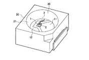
このような外囲器としては、例えば特許文献1に記載のものが知られている。図6の斜視図に示すように、従来の外囲器は、パッケージ20に内壁が傾斜した凹部21を備え、凹部21の底面に金属製のカソード側のリードフレーム11とアノード側のリードフレーム12が別々に配置される。発光素子1の下端の電極がリードフレーム11に銀ペースト等の導電性材料で接続され、発光素子1の上端の電極2がワイヤ3を通じてリードフレーム12に接続される。パッケージ20は、凹部21の内壁で完全拡散反射に近い条件で発光素子1からの光が反射されるように、白色のポリフタルアミド樹脂で形成される。凹部21には、上面開口部から透光性のエポキシ樹脂30が液体の状態で注入され、その後、エポキシ樹脂30は加温され硬化される。このような構成により、この外囲器は、発光素子1が発した直接光あるいは反射光をエポキシ樹脂30を介して外部へ放射するようになっている。 As such an envelope, for example, the one described in Patent Document 1 is known. As shown in the perspective view of FIG. 6, the conventional envelope includes a
また、図7の斜視図に示すように、白色を含めた混色を実現するために、複数の発光素子を外囲器に搭載することもある。同図では、RBG三色の発光素子1a,1b,1cの下端の電極が、それぞれ別個のカソード側のリードフレーム11a,11b,11c上に銀ペーストもしくは共晶半田で接続されている。そして、発光素子1a,1b,1cのそれぞれの上端の電極2a,2b,2cは、それぞれに対応するワイヤ3a,3b,3cを通じて共通のアノード側のリードフレーム12に接続される。
図6に示した構成の場合、発光素子1で発生した熱は、熱伝導性の良い金属を通して逃げることになる。つまり、発光素子1の下端の電極の底面が接続されたリードフレーム11を通じて熱が逃げる。一方、発光素子1の上端の電極に接続されているワイヤ3は細いため、このワイヤ3に接続されているリードフレーム12は、熱の放熱経路としてはほとんど寄与せず、この外囲器は放熱効率が低いという問題がある。 In the case of the configuration shown in FIG. 6, heat generated in the light emitting element 1 escapes through a metal having good thermal conductivity. That is, heat escapes through the
また、図7に示した構成では、3つの独立したリードフレーム11a,11b,11cは、発光素子1a,1b,1cの下端の電極の底面がそれぞれ接続されているので放熱に寄与するが、共通のリードフレーム12は、発光素子1a,1b,1cの上端の電極2a,2b,2cにそれぞれ細いワイヤ3a,3b,3cを通じて接続されているため、放熱にはほとんど寄与しない。よって、この外囲器も放熱効率は十分ではない。 In the configuration shown in FIG. 7, the three
本発明は、上記に鑑みてなされたものであり、その課題とするところは、発光素子の外囲器における放熱効率を改善することにある。 This invention is made | formed in view of the above, The place made into the subject is to improve the thermal radiation efficiency in the envelope of a light emitting element.
本発明に係る発光素子の外囲器は、上部がp型、下部がn型で上下両面に電極を備えた第1発光素子と、上部がn型、下部がp型で上下両面に電極を備えた第2発光素子と、第1発光素子の下面の電極が接続される第1リードフレームと、第2発光素子の下面の電極が接続される第2リードフレームと、第1発光素子の上面の電極と第2発光素子の上面の電極とを接続するワイヤと、を有することを特徴とする。 The envelope of the light emitting device according to the present invention includes a first light emitting device having a p-type upper portion and an n-type lower portion and electrodes on both upper and lower surfaces, an n-type upper portion, a p-type lower portion, and electrodes on both upper and lower surfaces. A second light emitting element, a first lead frame to which an electrode on the lower surface of the first light emitting element is connected, a second lead frame to which an electrode on the lower surface of the second light emitting element is connected, and an upper surface of the first light emitting element And a wire connecting the electrode of the second light emitting element and the electrode on the upper surface of the second light emitting element.
本発明にあっては、第1リードフレームに第1発光素子の下面の電極を接続し、第2リードフレームに第2発光素子の下面の電極を接続したことで、第1リードフレームと第2リードフレームの双方が放熱に寄与する。 In the present invention, the electrode on the lower surface of the first light emitting element is connected to the first lead frame, and the electrode on the lower surface of the second light emitting element is connected to the second lead frame. Both lead frames contribute to heat dissipation.
本発明の発光素子の外囲器によれば、放熱効率を大幅に改善することができる。 According to the envelope of the light emitting element of the present invention, the heat radiation efficiency can be greatly improved.
[第1の実施の形態]
図1は、第1実施形態における発光素子の外囲器の構成を示す斜視図である。同図の外囲器は、受けた光を完全拡散反射に近い条件で反射する白色のPPA(ポリフタルアミド)樹脂製の枠構造のパッケージ20に凹部を備え、この凹部の底面に金属製のリードフレーム11(第1リードフレーム)およびリードフレーム12(第2リードフレーム)がそれぞれ配置される。この凹部の底面には、LED(Light Emitting Diode)等による2種類の同色の発光素子1a(第1発光素子),発光素子1a’(第2発光素子)が配置される。[First Embodiment]
FIG. 1 is a perspective view showing a configuration of an envelope of a light emitting element in the first embodiment. The envelope shown in the figure is provided with a recess in a
図2(a)に示すように、発光素子1aは、通常のn型GaAs基板100上に、AllnGap系の赤色四元活性層101を含むダブルへテロ構造を有し、p側の上面に円形の電極2aを、n側の下面に矩形の電極4aをそれぞれ備える。 As shown in FIG. 2A, the
また、図2(b)に示すように、発光素子1a’は、発光素子1aをp型GaP基板200に融着させ、後からGaAs基板100をエッチングで除去して構成される。よって、発光素子1a’の最終構造としては、p型GaP基板200の上にAllnGap系赤色四元活性層101を含むダブルへテロ構造が形成され、n側の上面に円形の電極2a’を、p側の下面に矩形の電極4a’をそれぞれ備える。なお、融着の手法は、ウェハー同士を直接融着してもよいし、金属を介して融着してもよい。 As shown in FIG. 2B, the
図1に示すように、発光素子1aは、その下面の電極4aがリードフレーム11に接続され、発光素子1a’は、その下面の電極4a’がリードフレーム12に接続される。これらの接続には、銀ペーストもしくはAu−Sn等の共晶半田を用いる。発光素子1aの上面の電極2aと発光素子1a’の上面の電極2a’は、ワイヤ3を通じて直列に接続される。このような構成の凹部に、透明のエポキシ樹脂30を液体の状態で注入し、その後、加温して硬化させる。 As shown in FIG. 1, the
図3は、本外囲器におけるリードフレーム11,12の構造を示す斜視図である。同図では、リードフレームの構造が分かり易くなるように、パッケージ20の上部とエポキシ樹脂30を除去した状態を示している。発光素子1aが発した熱はリードフレーム11を通じて放熱され、発光素子1a’が発した熱はリードフレーム12を通じて放熱される。 FIG. 3 is a perspective view showing the structure of the
したがって、本実施の形態によれば、リードフレーム11に発光素子1aの下面の電極4aを接続し、別のリードフレーム12に発光素子1a’の下面の電極4a’を接続したことで、リードフレーム11,12の双方が放熱に寄与するので、放熱効率を大幅に向上させることができる。これによって、より大きな電流を流すことが可能となり、明るい発光色を得ることができる。 Therefore, according to the present embodiment, the
なお、本実施の形態において、図6に示した発光素子の外囲器と同じ明るさを得るためには、それぞれの発光素子1a,1a’に流す電流値は半分でよい。この半分の電流値に相当する熱がそれぞれリードフレーム11,12から放熱されるので、発光素子の温度上昇を有効に抑えることができる。 In this embodiment, in order to obtain the same brightness as that of the envelope of the light emitting element shown in FIG. 6, the value of the current passed through each of the
[第2の実施の形態]
図4は、第2実施形態における発光素子の外囲器の構成を示す斜視図である。本実施の形態では、発する光が同色の発光素子ではなく、異なる色の発光素子1a(第1発光素子),1b(第2発光素子)を用いる。本実施形態における発光素子1aは、n型SiC基板上に成長させたGaN/InGaN系の青色LEDであり、p側の上面に円形の電極2aを備え、n側の下面にも電極を備える。一方、発光素子1bは、p型GaP基板200の上にAllnGaP系の黄色四元活性層を含むダブルヘテロ構造を有する黄色LEDであり、n側の上面に円形の電極2bを備え、p側の下面にも電極を有する。[Second Embodiment]
FIG. 4 is a perspective view showing the configuration of the envelope of the light emitting element in the second embodiment. In the present embodiment, the light emitted from the
発光素子1aの下面の電極はリードフレーム11に接続され、発光素子1bの下面の電極はリードフレーム12に接続される。これらの接続には、銀ペーストもしくはAu−Sn等の共晶半田が用いられる。発光素子1aの上面の電極2aと発光素子1bの上面の電極2bは、ワイヤ3を通じて直列に接続される。その他、図1と同一物には同一の符号を付すものとし、ここでは重複した説明は省略する。 The electrode on the lower surface of the
本実施の形態によれば、発する光が異なる色の発光素子1a,1bを用い、その一例として青色LEDと黄色LEDを用いたことで、青色と黄色は補色関係にあるので、発光素子1a,1bが発する光は擬似白色となり、明るい白色発光を実現することができる。 According to the present embodiment, the
また、第1実施形態と同様に、リードフレーム11に発光素子1aの下面の電極を接続し、別のリードフレーム12に発光素子1bの下面の電極を接続したことで、リードフレーム11,12の双方が放熱に寄与するので、放熱効率を大幅に向上させることができる。 Further, as in the first embodiment, the electrodes on the lower surface of the
なお、本実施の形態においては、発光素子1a,1bが発する光をそれぞれ青色、黄色としたが、これに限られるものではなく、様々な色を適用することができる。 In the present embodiment, the light emitted from the
[第3の実施の形態]
図5は、第3実施形態における発光素子の外囲器の構成を示す斜視図である。本実施の形態では、第1発光素子と第2発光素子の組を複数設けた外囲器について説明する。同図の発光素子1a,1bは、図4に示した発光素子1a,1bと同一物であり、リードフレーム11,12にそれぞれ接続される。本実施形態では、この他にもう一組の発光素子1c,1dを用いる。[Third Embodiment]
FIG. 5 is a perspective view showing the configuration of the envelope of the light emitting element in the third embodiment. In this embodiment, an envelope provided with a plurality of sets of first light emitting elements and second light emitting elements will be described. The
発光素子1cは、n型SiC基板上に成長させたGaN/InGaN系の緑色LEDであり、p側の上面に円形の電極2cを備え、n側の下面にも電極も備える。発光素子1dは、p型GaP基板上にAllnGaP系の赤色四元活性層101を含むダブルへテロ構造を有する赤色LEDであり、n側の上面に円形の電極2dを備え、p側の下面にも電極を備える。 The light-emitting
発光素子1cの下面の電極はリードフレーム11に接続され、発光素子1dの下面の電極はリードフレーム12に接続される。これらの接続には、銀ペーストもしくはAu−Sn等の共晶半田が用いられる。発光素子1cの上面の電極2cと発光素子1dの上面の電極2dは、ワイヤ3bを通じて直列に接続される。その他、図4と同一物には同一の符号を付すものとし、ここでは重複した説明は省略する。 The electrode on the lower surface of the
このような構成とすることで、発光素子1a,1cが発した熱はリードフレーム11を通じて放熱され、発光素子1b,1dが発した熱はリードフレーム12を通じて放熱される。 With this configuration, heat generated by the
したがって、本実施の形態によれば、4つの発光素子1a〜1dを集積化したパッケージでも、リードフレーム11に発光素子1a,1cのそれぞれの下面の電極を接続し、別のリードフレーム12に発光素子1b、1dの下面の電極を接続したことで、発光素子1a,1cが発した熱はリードフレーム11から放熱され、発光素子1b、1dが発した熱はリードフレーム12から放熱されるので、リードフレーム11,12の双方が放熱に寄与し、放熱効率を大幅に向上させることができる。これによって、より大きな電流を流すことが可能となり、明るい発光色を得ることができる。 Therefore, according to the present embodiment, even in a package in which the four
また、本実施の形態によれば、発光素子の色の種類を多くできるので、より演色性の良い白色発光を実現することができる。 Further, according to the present embodiment, since the types of colors of the light emitting elements can be increased, white light emission with better color rendering can be realized.
なお、直列に接続した発光素子1a,1bの組と、発光素子1c、1dの組については、それぞれの直列電圧と直列抵抗はほぼ同じになるように、発光波長および素子の構造を選択することが望ましい。これにより、直列に接続された発光素子に流れる電流値を、双方の組でほぼ等しくすることができる。 In addition, for the set of
1,1a,1a’,1b,1c,1d…発光素子
2,2a,2b,2c…電極
3,3a,3b,3c…ワイヤ
4a,4a’…電極
11,11a,11b,11c…リードフレーム
12…リードフレーム
20…パッケージ
21…凹部
30…エポキシ樹脂
100…n型GaAs基板
101…赤色四元活性層
200…p型GaP基板
DESCRIPTION OF
Claims (4)
Translated fromJapanese上部がn型、下部がp型で上下両面に電極を備えた第2発光素子と、
第1発光素子の下面の電極が接続される第1リードフレームと、
第2発光素子の下面の電極が接続される第2リードフレームと、
第1発光素子の上面の電極と第2発光素子の上面の電極とを接続するワイヤと、
を有することを特徴とする発光素子の外囲器。A first light-emitting element having an upper part of p-type, a lower part of n-type, and electrodes on both upper and lower sides;
A second light emitting device having an n-type upper portion and a p-type lower portion and electrodes on both upper and lower surfaces;
A first lead frame to which an electrode on the lower surface of the first light emitting element is connected;
A second lead frame to which an electrode on the lower surface of the second light emitting element is connected;
A wire connecting the electrode on the upper surface of the first light emitting element and the electrode on the upper surface of the second light emitting element;
An envelope of a light-emitting element, comprising:
The envelope of the light emitting element according to any one of claims 1 to 3, wherein a plurality of sets of the first light emitting element and the second light emitting element are provided.
Priority Applications (1)
| Application Number | Priority Date | Filing Date | Title |
|---|---|---|---|
| JP2004351150AJP2006165097A (en) | 2004-12-03 | 2004-12-03 | Light emitting device envelope |
Applications Claiming Priority (1)
| Application Number | Priority Date | Filing Date | Title |
|---|---|---|---|
| JP2004351150AJP2006165097A (en) | 2004-12-03 | 2004-12-03 | Light emitting device envelope |
Publications (1)
| Publication Number | Publication Date |
|---|---|
| JP2006165097Atrue JP2006165097A (en) | 2006-06-22 |
Family
ID=36666786
Family Applications (1)
| Application Number | Title | Priority Date | Filing Date |
|---|---|---|---|
| JP2004351150AAbandonedJP2006165097A (en) | 2004-12-03 | 2004-12-03 | Light emitting device envelope |
Country Status (1)
| Country | Link |
|---|---|
| JP (1) | JP2006165097A (en) |
Cited By (4)
| Publication number | Priority date | Publication date | Assignee | Title |
|---|---|---|---|---|
| CN102032485A (en)* | 2009-09-29 | 2011-04-27 | 丰田合成株式会社 | Lighting device |
| WO2011093174A1 (en)* | 2010-01-29 | 2011-08-04 | 日本航空電子工業株式会社 | Led device, manufacturing method thereof, and light-emitting device |
| US9006759B2 (en) | 2010-04-15 | 2015-04-14 | Citizen Electronics Co., Ltd. | Light-emitting device |
| JP6033982B1 (en)* | 2010-06-01 | 2016-11-30 | エルジー イノテック カンパニー リミテッド | Light emitting device package |
Citations (2)
| Publication number | Priority date | Publication date | Assignee | Title |
|---|---|---|---|---|
| JPS6275697A (en)* | 1985-09-30 | 1987-04-07 | タキロン株式会社 | Light emitting display unit using light emitting diode chip |
| JP2003008075A (en)* | 2001-06-27 | 2003-01-10 | Toyoda Gosei Co Ltd | LED lamp |
- 2004
- 2004-12-03JPJP2004351150Apatent/JP2006165097A/ennot_activeAbandoned
Patent Citations (2)
| Publication number | Priority date | Publication date | Assignee | Title |
|---|---|---|---|---|
| JPS6275697A (en)* | 1985-09-30 | 1987-04-07 | タキロン株式会社 | Light emitting display unit using light emitting diode chip |
| JP2003008075A (en)* | 2001-06-27 | 2003-01-10 | Toyoda Gosei Co Ltd | LED lamp |
Cited By (14)
| Publication number | Priority date | Publication date | Assignee | Title |
|---|---|---|---|---|
| CN102032485A (en)* | 2009-09-29 | 2011-04-27 | 丰田合成株式会社 | Lighting device |
| JP5871621B2 (en)* | 2010-01-29 | 2016-03-01 | 日本航空電子工業株式会社 | LED device, manufacturing method thereof, and light emitting device |
| KR101398701B1 (en)* | 2010-01-29 | 2014-05-27 | 니혼 고꾸 덴시 고교 가부시끼가이샤 | Led device, manufacturing method thereof, and light-emitting device |
| TWI467816B (en)* | 2010-01-29 | 2015-01-01 | Japan Aviation Electron | LED device, manufacturing method thereof and illuminating device |
| WO2011093174A1 (en)* | 2010-01-29 | 2011-08-04 | 日本航空電子工業株式会社 | Led device, manufacturing method thereof, and light-emitting device |
| US9425372B2 (en) | 2010-01-29 | 2016-08-23 | Japan Aviation Electronics Industry, Limited | LED device, method of manufacturing the same, and light-emitting apparatus |
| US9006759B2 (en) | 2010-04-15 | 2015-04-14 | Citizen Electronics Co., Ltd. | Light-emitting device |
| US9224720B2 (en) | 2010-04-15 | 2015-12-29 | Citizen Electronics Co., Ltd. | Light-emitting device including light-emitting diode element that is mounted on outer portion of electrode |
| JP6033982B1 (en)* | 2010-06-01 | 2016-11-30 | エルジー イノテック カンパニー リミテッド | Light emitting device package |
| US9991241B2 (en) | 2010-06-01 | 2018-06-05 | Lg Innotek Co., Ltd. | Light emitting device package |
| JP2018137471A (en)* | 2010-06-01 | 2018-08-30 | エルジー イノテック カンパニー リミテッド | Light emitting element package |
| US10283491B2 (en) | 2010-06-01 | 2019-05-07 | Lg Innotek Co., Ltd | Light emitting device package |
| JP2019106551A (en)* | 2010-06-01 | 2019-06-27 | エルジー イノテック カンパニー リミテッド | Light-emitting element package |
| US10541235B2 (en) | 2010-06-01 | 2020-01-21 | Lg Innotek Co., Ltd. | Light emitting device package |
Similar Documents
| Publication | Publication Date | Title |
|---|---|---|
| JP5813086B2 (en) | LED package and manufacturing method thereof | |
| JP6025787B2 (en) | Light emitting diode package | |
| TWI523273B (en) | Light-emitting diode package with contrast surface | |
| KR20100077909A (en) | Lighting emitting device package and fabrication method thereof | |
| JP2004207367A (en) | Light emitting diode and light emitting diode arrangement plate | |
| JP4277508B2 (en) | Semiconductor light emitting device | |
| JP2001077427A (en) | Light-emitting diode and display device using the same | |
| JP4821343B2 (en) | Submount substrate and light emitting device including the same | |
| JP2007243054A (en) | Light-emitting device | |
| KR100849828B1 (en) | Light emitting diode package | |
| KR101163850B1 (en) | Light emitting device package | |
| KR100643582B1 (en) | Light emitting diode package | |
| US20060006793A1 (en) | Deep ultraviolet used to produce white light | |
| JP2006344717A (en) | Light-emitting device and its manufacturing method | |
| JP2006165097A (en) | Light emitting device envelope | |
| JP2007088078A (en) | Light-emitting device | |
| KR101778141B1 (en) | Semiconductor light emitting device and method of manufacturing the same | |
| JP2009099823A (en) | Light-emitting device | |
| JP2007053320A (en) | Led lighting device | |
| KR20050101737A (en) | Light emitting diode package | |
| KR100601197B1 (en) | Light emitting diode | |
| JP2007080867A (en) | Light emitting device | |
| US20250054920A1 (en) | Multiple chip led packages with common electrodes | |
| JP2007243057A (en) | Light-emitting device | |
| KR100591943B1 (en) | Light emitting diode |
Legal Events
| Date | Code | Title | Description |
|---|---|---|---|
| A621 | Written request for application examination | Free format text:JAPANESE INTERMEDIATE CODE: A621 Effective date:20071130 | |
| A977 | Report on retrieval | Free format text:JAPANESE INTERMEDIATE CODE: A971007 Effective date:20100622 | |
| A131 | Notification of reasons for refusal | Free format text:JAPANESE INTERMEDIATE CODE: A131 Effective date:20100629 | |
| A762 | Written abandonment of application | Free format text:JAPANESE INTERMEDIATE CODE: A762 Effective date:20100830 |