JP2006156776A - Semiconductor device - Google Patents
Semiconductor deviceDownload PDFInfo
- Publication number
- JP2006156776A JP2006156776AJP2004346328AJP2004346328AJP2006156776AJP 2006156776 AJP2006156776 AJP 2006156776AJP 2004346328 AJP2004346328 AJP 2004346328AJP 2004346328 AJP2004346328 AJP 2004346328AJP 2006156776 AJP2006156776 AJP 2006156776A
- Authority
- JP
- Japan
- Prior art keywords
- type semiconductor
- semiconductor layer
- layer
- electrode
- gaas layer
- Prior art date
- Legal status (The legal status is an assumption and is not a legal conclusion. Google has not performed a legal analysis and makes no representation as to the accuracy of the status listed.)
- Pending
Links
Images


Classifications
- H—ELECTRICITY
- H10—SEMICONDUCTOR DEVICES; ELECTRIC SOLID-STATE DEVICES NOT OTHERWISE PROVIDED FOR
- H10D—INORGANIC ELECTRIC SEMICONDUCTOR DEVICES
- H10D84/00—Integrated devices formed in or on semiconductor substrates that comprise only semiconducting layers, e.g. on Si wafers or on GaAs-on-Si wafers
- H10D84/101—Integrated devices comprising main components and built-in components, e.g. IGBT having built-in freewheel diode
- H10D84/121—BJTs having built-in components
- H10D84/125—BJTs having built-in components the built-in components being resistive elements, e.g. BJT having a built-in ballasting resistor
- H—ELECTRICITY
- H10—SEMICONDUCTOR DEVICES; ELECTRIC SOLID-STATE DEVICES NOT OTHERWISE PROVIDED FOR
- H10D—INORGANIC ELECTRIC SEMICONDUCTOR DEVICES
- H10D10/00—Bipolar junction transistors [BJT]
- H10D10/80—Heterojunction BJTs
- H10D10/821—Vertical heterojunction BJTs
- H—ELECTRICITY
- H10—SEMICONDUCTOR DEVICES; ELECTRIC SOLID-STATE DEVICES NOT OTHERWISE PROVIDED FOR
- H10D—INORGANIC ELECTRIC SEMICONDUCTOR DEVICES
- H10D84/00—Integrated devices formed in or on semiconductor substrates that comprise only semiconducting layers, e.g. on Si wafers or on GaAs-on-Si wafers
- H10D84/01—Manufacture or treatment
- H10D84/02—Manufacture or treatment characterised by using material-based technologies
- H10D84/05—Manufacture or treatment characterised by using material-based technologies using Group III-V technology
Landscapes
- Bipolar Transistors (AREA)
Abstract
Description
Translated fromJapanese本発明は、半導体装置に係り、特に、高周波電力用途に好適な半導体装置に関する。 The present invention relates to a semiconductor device, and more particularly to a semiconductor device suitable for high frequency power applications.
高周波電力用途、例えば携帯電話の最終出力段の電力増幅には、InGaP/GaAsのヘテロ接合を有するHTB(heterojunction bipolar transistor)が用いられている。携帯電話のような分野では電力増幅器としてその効率の向上は通話可能時間の延長につながり重要である。HBTを用いた電力増幅器で効率を向上するには、HBTのコレクタ・エミッタ間電圧対コレクタ電流の特性における、いわゆるニー電圧(ゼロから立ち上がったコレクタ電流がほぼ一定の値に移行するときのコレクタ・エミッタ間電圧)を下げることが効果的である。一般的にニー電圧は、エミッタ抵抗およびコレクタ抵抗を下げることで小さくできる。 An HTB (heterojunction bipolar transistor) having an InGaP / GaAs heterojunction is used for high-frequency power applications, for example, power amplification at the final output stage of a mobile phone. In a field such as a cellular phone, improvement of the efficiency as a power amplifier is important because it extends the available communication time. In order to improve the efficiency of the power amplifier using the HBT, the so-called knee voltage (the collector current when the collector current rising from zero shifts to a substantially constant value) in the collector-emitter voltage vs. collector current characteristic of the HBT is shown. It is effective to lower the emitter voltage. Generally, the knee voltage can be reduced by lowering the emitter resistance and the collector resistance.
電力用途のデバイスでは特に、半導体基板上に形成された複数の素子を並列に接続してひとつのデバイスとして用いる場合が多く、このような場合、エミッタ抵抗を下げると熱暴走が発生しやすくなる。熱暴走とは、デバイスなどが発生する熱により温度が上昇するとわずかに温度が高い素子に電流が集中し始めこれによりその素子がさらに熱を発生して電流集中し故障もしくは破壊に至る現象である。 In particular, devices for electric power use are often used as a single device by connecting a plurality of elements formed on a semiconductor substrate in parallel. In such a case, if the emitter resistance is lowered, thermal runaway tends to occur. Thermal runaway is a phenomenon in which when the temperature rises due to the heat generated by a device, etc., current starts to concentrate on elements that are slightly higher in temperature, causing the elements to generate more heat, causing current concentration and failure or destruction. .
熱暴走を抑制するには、各素子のベースに抵抗(バラスト抵抗)を挿入する構成が有効であるが、一方で挿入した抵抗によって周波数特性は劣化する。周波数特性の確保と熱暴走の抑制を両立するための技術には例えば下記特許文献1に記載のものがある。この技術では、ベースへのRF信号の入力のための電極とバイアス電圧を印加のための電極とが別々に設けられ、バイアス印加の電極からベース層までのベース層延設部がバラスト抵抗として機能するようにしている。この構成は、ベース層の延設によりベース・コレクタ間容量が増加し、さらなる周波数特性の確保には困難が伴うと考えられる。
本発明は、上記した事情を考慮してなされたもので、熱暴走の抑制とさらなる周波数特性の確保との両立を図ることが可能な半導体装置を提供することを目的とする。 The present invention has been made in consideration of the above-described circumstances, and an object thereof is to provide a semiconductor device capable of achieving both suppression of thermal runaway and ensuring of further frequency characteristics.
本発明の一態様に係る半導体装置は、半導体基板と、前記半導体基板上に形成されたn+型半導体層と、前記n+型半導体層上に形成された第1のn型半導体層と、前記第1のn型半導体層上に形成され、第1のバンドギャップを有する材料のp型半導体層と、前記p型半導体層上に形成され、前記p型半導体層より面積が小さくかつ前記第1のバンドギャップより大きな第2のバンドギャップを有する材料の第2のn型半導体層と、前記第2のn型半導体層が形成されていない領域の前記p型半導体層から前記第1のn型半導体層および前記n+型半導体層を貫通して前記半導体基板に達して形成され、前記p型半導体層、前記第1のn型半導体層、および前記n+型半導体層を2つの領域に分断するインプラント部と、前記第2のn型半導体層が形成されていない領域の前記p型半導体層上に、かつ少なくとも前記インプラント部をまたいで形成された電極とを具備することを特徴とする。A semiconductor device according to one embodiment of the present invention includes a semiconductor substrate, an n+ type semiconductor layer formed over the semiconductor substrate, a first n type semiconductor layer formed over the n+ type semiconductor layer, A p-type semiconductor layer formed on the first n-type semiconductor layer and made of a material having a first bandgap; and formed on the p-type semiconductor layer and having a smaller area than the p-type semiconductor layer; A first n-type semiconductor layer made of a material having a second band gap larger than one band gap and the p-type semiconductor layer in a region where the second n-type semiconductor layer is not formed. through type semiconductor layer and the n+ -type semiconductor layer is formed to reach the semiconductor substrate, the p-type semiconductor layer, the first n-type semiconductor layer, and the n+ -type semiconductor layer into two regions The implant part to be cut and the second n-type And an electrode formed on at least the implant portion on the p-type semiconductor layer in a region where the semiconductor layer is not formed.
本発明の半導体装置によれば、熱暴走の抑制とさらなる周波数特性の確保との両立を図ることができる。 According to the semiconductor device of the present invention, both suppression of thermal runaway and securing of further frequency characteristics can be achieved.
本発明の一態様に係る半導体装置によれば、p型半導体層が、第1のn型半導体層およびn+型半導体層とともにインプラント部により2つの領域に分断されている。そして、第2のn型半導体層が形成されていない領域のp型半導体層上に、かつ少なくともインプラント部をまたいで電極が形成されている。このような構造により、p型半導体層の一方の領域をバラスト抵抗としての領域にすることが可能であり、しかも、この領域のp型半導体層とその下側のn型半導体層との接合が、インプラント部により活性領域とは分離されるので、トランジスタとしてのベース・コレクタ間容量となるのが防止されている。よって、熱暴走の抑制とさらなる周波数特性の確保との両立を図ることができる。According to the semiconductor device of one embodiment of the present invention, the p-type semiconductor layer is divided into two regions by the implant portion together with the first n-type semiconductor layer and the n+ -type semiconductor layer. An electrode is formed on the p-type semiconductor layer in a region where the second n-type semiconductor layer is not formed and at least across the implant portion. With such a structure, it is possible to make one region of the p-type semiconductor layer a region as a ballast resistor, and the junction between the p-type semiconductor layer in this region and the n-type semiconductor layer therebelow is formed. Since the active region is separated by the implant portion, the base-collector capacitance as a transistor is prevented. Therefore, both suppression of thermal runaway and securing of further frequency characteristics can be achieved.
本発明の実施態様として、前記電極は、前記インプラント部をまたいでいる部位でくびれた平面形状を有する、としてもよい。電極とn+型半導体層とにより寄生的に形成される容量分をできるだけ小さくするためである。これによりさらにベース・コレクタ間容量が減少し好ましい。As an embodiment of the present invention, the electrode may have a planar shape constricted at a portion straddling the implant portion. This is to make the capacitance parasitically formed by the electrode and the n+ type semiconductor layer as small as possible. This further reduces the base-collector capacitance, which is preferable.
また、実施態様として、前記p型半導体層の前記第1のバンドギャップを有する前記材料は、GaAsまたはGaAsSbを主要な組成とする、とすることができる。また、前記第2のn型半導体層の前記第2のバンドギャップを有する前記材料は、InGaPを主要な組成とする、とすることができる。HBTのヘテロジャンクションを実現する一例である。 As an embodiment, the material having the first band gap of the p-type semiconductor layer may have GaAs or GaAsSb as a main composition. The material having the second band gap of the second n-type semiconductor layer may be mainly composed of InGaP. It is an example which implement | achieves the heterojunction of HBT.
また、実施態様として、前記電極は、前記第2のn型半導体層を挟んで前記インプラント部の反対側までの広がりで形成され、該反対側に信号入力接続部を有する、とすることができる。RF入力のための接続をインプラント部の反対側で行うものである。カップリングコンデンサを内蔵する場合のレイアウトが容易になる。 As an embodiment, the electrode may be formed so as to extend to the opposite side of the implant portion with the second n-type semiconductor layer interposed therebetween, and may have a signal input connection portion on the opposite side. . The connection for the RF input is made on the opposite side of the implant part. The layout when the coupling capacitor is built-in becomes easy.
また、実施態様として、前記p型半導体層は、ほぼ50nmの厚さで形成されている、とすることができる。高周波用途に適合させるためである。 As an embodiment, the p-type semiconductor layer may be formed with a thickness of approximately 50 nm. This is to adapt to high frequency applications.
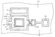
以上を踏まえ、以下では本発明の実施形態を図面を参照しながら説明する。図1は、本発明の一実施形態に係る半導体装置(HBT)の模式的構造を示す平面図である。図1に示すように、このHBT10は、素子分離膜13により他の領域と素子分離されて形成され、n+−GaAs層(n+型半導体層)12、コレクタ電極14、p+−GaAs層(p型半導体層)16、ベース電極17、信号入力接続部(RF入力ポート)18、直流入力電極(DC入力ポート)19、n−GaAs層21、エミッタ電極22、インプラント部23を有する。Based on the above, embodiments of the present invention will be described below with reference to the drawings. FIG. 1 is a plan view showing a schematic structure of a semiconductor device (HBT) according to an embodiment of the present invention. As shown in FIG. 1, the
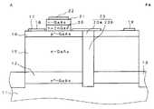
図2は、図1中に示すA−Aaにおける矢視方向の模式的な断面図である。このHBTは、図1に図示された構成要素のほか縦方向に重畳してさらに、絶縁性(半絶縁性)の半導体基板(GaAs基板)11、n−GaAs層(第1のn型半導体層)15、n−InGaP層(第2のn型半導体層)20を有する。インプラント部23は、p+−GaAs層16へのインプラント部23aと、n−GaAs層とn+−GaAs層へのインプラント部23bとに便宜上分けて図示している。FIG. 2 is a schematic cross-sectional view in the direction of the arrow in A-Aa shown in FIG. This HBT overlaps in the vertical direction in addition to the components shown in FIG. 1, and further includes an insulating (semi-insulating) semiconductor substrate (GaAs substrate) 11, an n-GaAs layer (first n-type semiconductor layer). ) 15 and an n-InGaP layer (second n-type semiconductor layer) 20. The
図3は、図1中に示すB−Baにおける矢視方向の模式的な断面図である。図4は、図1中に示すC−Caにおける矢視方向の模式的な断面図である。図3、図4中に使用される符号は図1、図2のものと共通する。 FIG. 3 is a schematic cross-sectional view in the direction of the arrow in B-Ba shown in FIG. FIG. 4 is a schematic cross-sectional view in the direction of the arrow in C-Ca shown in FIG. The reference numerals used in FIGS. 3 and 4 are the same as those in FIGS.
図1ないし図4に示されるように、このHBT10は、半導体基板11上に形成されたn+−GaAs層12(厚さ例えば500nm)上一部にコレクタ電極14を有する。n+−GaAs層12上のコレクタ電極14のない領域はコレクタ電極14の近傍を除いて、n−GaAs層15層(厚さ例えば700nm)が積層形成され、n−GaAs層15層上にはp+−GaAs層16(厚さ例えば50nm)が積層形成されている。さらに、p+−GaAs層16上の一部にn−InGaP層20(厚さ例えば20nm)が積層形成され、n−InGaP層20上にはn−GaAs層21(厚さ例えば100nm)が積層形成されている。また、n−GaAs層21上にはエミッタ電極22が積層形成されている。As shown in FIGS. 1 to 4, the
p+−GaAs層16、n−GaAs層15、n+−GaAs層12は、半導体基板11に達して形成されたインプラント部23によりふたつの領域に分断されており、図示左側のn−InGaP層20、n−GaAs層21を有する側が実質のトランジスタとして機能する領域(=活性領域)である。ここで、n+−GaAs層12はコレクタコンタクト層として、n−GaAs層15はコレクタ層として、p+−GaAs層16はベース層として、n−InGaP層20はエミッタ層として、n−GaAs層21はエミッタコンタクト層としてそれぞれ機能する。p+−GaAs層16のベース層とn−InGaP層20のエミッタ層との接合がヘテロ接合である。The p+ -
ベース電極17は、p+−GaAs層16上の、n−InGaP層20が形成されていない領域上に形成されており、より詳しくは、n−InGaP層20を取り囲むようにかつインプラント部23をまたぐように形成されている。ベース電極17の、エミッタ電極22をはさんでインプラント部23の形成された側と反対の側一部が信号入力接続部18となる。直流入力電極19は、インプラント部23により分断されたp+−GaAs層16の、インプラント部23から離れた端部近傍上に設けられる。The
各層における不純物ドーピング濃度を例示すると、n+−GaAs層12が5×1018cm−3、n−GaAs層15が1×1016cm−3、p+−GaAs層16が4×1019cm−3、n−InGaP層20が4×1017cm−3、n−GaAs層21が5×1018cm−3である。インプラント部23は、n+−GaAs層12、n−GaAs層15層、p+−GaAs層16が積層形成されたあとに、p+−GaAs層16上側から半導体基板11中に達するイオン注入を行いこれらの層を高抵抗化した部位である。p+−GaAs層16へのインプラント部23aは、もともとの不純物濃度が高いため他のインプラント部23bに比較して抵抗値は低い。The impurity doping concentration in each layer is exemplified. The n+ -
各部の平面的なサイズは、p+−GaAs層16の上下最大が例えば5μm、同じくp+−GaAs層16の活性領域における左右最大が例えば20μmである。ベース電極17の上下最大が例えば4μm、エミッタ電極22の上下最大が例えば2μmである。Planar size of eachpart, the upper and lower maximum eg 5μm of p + -
p+−GaAs層16の、直流入力電極19直下から、インプラント部23をまたいで直流入力電極19の側に延長形成されたベース電極17に至る部位、およびp+−GaAs層16へのインプラント部23aは、ベースに挿入された抵抗として機能する部位である。ただしこのうちp+−GaAs層16へのインプラント部23aはベース電極17が並列するので抵抗としての寄与は小さい。A portion of the p+ -
ベース抵抗としての値は、この部位のp+−GaAs層16の不純物濃度や、長さや幅、厚さなどの形状を制御して必要な値に設計することができる。必要な値の具体例として例えば1kΩ程度を挙げることができる。このベース抵抗としての部位はn−GaAs層15とのpn接合を有するが、インプラント部23により分断され活性でないn−GaAs層15領域とのpn接合なので、コレクタ・ベース間容量の増加にはならない。しがたって高周波特性を劣化される恐れがない。The value as the base resistance can be designed to a required value by controlling the impurity concentration, length, width, thickness, and the like of the p+ -
このHBT10を携帯電話の出力最終段のパワーアンプに使用するとき、動作条件としては例えば、電源電圧Vcc=3.5V、コレクタ電流Ic=5mA、周波数帯域f=800MHz〜5GHzにすることができる。この場合実際には、HBT10を同一半導体チップ上に複数(例えば50ないし100)作り込み、これらを並列に接続して高周波で大電流、大出力(例えば1Wないし3W)のデバイスとして使用する。 When this
図5は、このような態様を説明するもので、図1に示した半導体装置(HBT10)をパラレルに複数使用する場合の例示的な模式的レイアウト図である。図5においてすでに説明した部位と同一相当のものには同一符号を付してある。図5に示すように、各HBT10は、p+−GaAs層16の長手方向が互いに平行になるようにかつエミッタ電極22とコレクタ電極14とを結ぶ線が一直線に並ぶように配置される。これにより、各直流入力電極19をコンタクト51を介して配線52により電気的接続する。配線52により各直流入力電極19には同一の直流電圧が供給される。FIG. 5 illustrates such an aspect, and is an exemplary schematic layout diagram when a plurality of semiconductor devices (HBTs 10) shown in FIG. 1 are used in parallel. In FIG. 5, the same parts as those already described are denoted by the same reference numerals. As shown in FIG. 5, the
また、ベース電極17の、エミッタ電極22をはさんでインプラント部23の側とは反対の側に設けられた信号入力接続部18には、キャパシタ(カップリングコンデンサ)53を介して配線54が配置され接続される。キャパシタ53は周知の構造でHBT10と同一チップ上に作り込むことができる。配線54により電力増幅すべき信号が各キャパシタ53を介して各ベース電極18に供給される。なお、配線54は、キャパシタ53を作り込む領域の確保がレイアウト上やや難しくなるが、エミッタ電極22をはさんで図示とは反対側に配置することも可能である。 In addition, a
以上説明したように、本実施携帯の半導体装置(HBT10)によれば、p+−GaAs層16が、n−GaAs層15およびn+−GaAs層12とともにインプラント部23により2つの領域に分断されている。そして、n−InGaP層20が形成されていない領域のp+−GaAs層16上に、かつ少なくともインプラント部23をまたいでベース電極17が形成されている。このような構造により、p+−GaAs層16の一方の領域をバラスト抵抗としての領域にすることが可能であり、しかも、この領域のp+−GaAs層16とその下側のn−GaAs層15との接合が、インプラント部23により活性領域とは分離されるので、トランジスタとしてのベース・コレクタ間容量の増加となるのが防止されている。よって、熱暴走の抑制とさらなる周波数特性の確保との両立を図ることができる。As described above, according to the portable semiconductor device (HBT 10) of this embodiment, the p+ -
次に、本発明の別の実施形態に係る半導体装置(HBT)について図6を参照して説明する。図6は、本発明の別の実施形態に係る半導体装置(HBT)の模式的構造を示す平面図である。図6において、すでに説明した部位には同一符号を付しその説明を省略する。さらに、図2ないし図4に相当する断面図の表示も図6に示す平面図から自明なので図示省略する。 Next, a semiconductor device (HBT) according to another embodiment of the present invention will be described with reference to FIG. FIG. 6 is a plan view showing a schematic structure of a semiconductor device (HBT) according to another embodiment of the present invention. In FIG. 6, the parts already described are assigned the same reference numerals, and the description thereof is omitted. Further, the display of cross-sectional views corresponding to FIGS. 2 to 4 is also omitted from the plan view shown in FIG.
この実施形態では、インプラント部23Aが形成される領域で、p+−GaAs層16Aおよびベース電極17Aが平面図としてくびれを有している。他の部分は上記の実施形態と同じである。このような形状にp+−GaAs層16Aおよびベース電極17Aを形成することで、ベース電極17Aとコレクタコンタクト層であるn+−GaAs層12との対向面積(やや斜めに対向ではあるが)を減少させることができる。したがって、ベース・コレクタ間容量を上記の実施形態の場合より小さくできる。よって、さらに高周波特性の向上が見込める。In this embodiment, the p+ -
この実施形態は、p+−GaAs層16Aとベース電極17Aとの接触面積が、インプラント部23をまたいだ両側では、ふたつに分断されたp+−GaAs層16Aを電気的導通させるためそれなりに確保される必要があるところ、インプラント部23A上では接触面積が小さくてもよいことに着目して得られたものである。In this embodiment, the contact area between the p+ -
なお、以上の実施形態では、p型半導体層(ベース層)としてp+−GaAs層16、同16Aを有するHBTの場合を示したが、ベース層としてはほかにp+−GaAsSbを用いることも可能である。In the above embodiment, the case of the HBT having the p+ -
10…ヘテロ接合バイポーラトランジスタ(HBT)、11…半導体基板(GaAs基板)、12…n+−GaAs層、13…素子分離膜、14…コレクタ電極、15…n−GaAs層、16、16A…p+−GaAs層、17、17A…ベース電極、18…信号入力接続部、19…直流入力電極、20…n−InGaP層、21…n−GaAs層、22…エミッタ電極、23、23A…インプラント部、23a…p+−GaAs層へのインプラント部、23b…n−GaAs層とn+−GaAs層へのインプラント部、51…コンタクト、52…配線、53…キャパシタ(カップリングコンデンサ)、54…配線。DESCRIPTION OF
Claims (5)
Translated fromJapanese前記半導体基板上に形成されたn+型半導体層と、
前記n+型半導体層上に形成された第1のn型半導体層と、
前記第1のn型半導体層上に形成され、第1のバンドギャップを有する材料のp型半導体層と、
前記p型半導体層上に形成され、前記p型半導体層より面積が小さくかつ前記第1のバンドギャップより大きな第2のバンドギャップを有する材料の第2のn型半導体層と、
前記第2のn型半導体層が形成されていない領域の前記p型半導体層から前記第1のn型半導体層および前記n+型半導体層を貫通して前記半導体基板に達して形成され、前記p型半導体層、前記第1のn型半導体層、および前記n+型半導体層を2つの領域に分断するインプラント部と、
前記第2のn型半導体層が形成されていない領域の前記p型半導体層上に、かつ少なくとも前記インプラント部をまたいで形成された電極と
を具備することを特徴とする半導体装置。A semiconductor substrate;
An n+ type semiconductor layer formed on the semiconductor substrate;
A first n-type semiconductor layer formed on the n+ -type semiconductor layer;
A p-type semiconductor layer formed on the first n-type semiconductor layer and made of a material having a first band gap;
A second n-type semiconductor layer formed on the p-type semiconductor layer and having a second band gap smaller in area than the p-type semiconductor layer and larger than the first band gap;
The p-type semiconductor layer in a region where the second n-type semiconductor layer is not formed penetrates the first n-type semiconductor layer and the n+ -type semiconductor layer and reaches the semiconductor substrate. an implant part for dividing the p-type semiconductor layer, the first n-type semiconductor layer, and the n+ -type semiconductor layer into two regions;
A semiconductor device comprising: an electrode formed on the p-type semiconductor layer in a region where the second n-type semiconductor layer is not formed and straddling at least the implant portion.
Priority Applications (2)
| Application Number | Priority Date | Filing Date | Title |
|---|---|---|---|
| JP2004346328AJP2006156776A (en) | 2004-11-30 | 2004-11-30 | Semiconductor device |
| US11/288,117US7323728B2 (en) | 2004-11-30 | 2005-11-29 | Semiconductor device |
Applications Claiming Priority (1)
| Application Number | Priority Date | Filing Date | Title |
|---|---|---|---|
| JP2004346328AJP2006156776A (en) | 2004-11-30 | 2004-11-30 | Semiconductor device |
Publications (1)
| Publication Number | Publication Date |
|---|---|
| JP2006156776Atrue JP2006156776A (en) | 2006-06-15 |
Family
ID=36594561
Family Applications (1)
| Application Number | Title | Priority Date | Filing Date |
|---|---|---|---|
| JP2004346328APendingJP2006156776A (en) | 2004-11-30 | 2004-11-30 | Semiconductor device |
Country Status (2)
| Country | Link |
|---|---|
| US (1) | US7323728B2 (en) |
| JP (1) | JP2006156776A (en) |
Families Citing this family (2)
| Publication number | Priority date | Publication date | Assignee | Title |
|---|---|---|---|---|
| TWI540722B (en)* | 2013-04-17 | 2016-07-01 | Win Semiconductors Corp | Heterojunction bipolar transistor layout structure |
| JP2015073001A (en)* | 2013-10-02 | 2015-04-16 | 三菱電機株式会社 | Semiconductor element |
Family Cites Families (20)
| Publication number | Priority date | Publication date | Assignee | Title |
|---|---|---|---|---|
| US4573064A (en)* | 1981-11-02 | 1986-02-25 | Texas Instruments Incorporated | GaAs/GaAlAs Heterojunction bipolar integrated circuit devices |
| JPH02297942A (en)* | 1989-05-11 | 1990-12-10 | Mitsubishi Electric Corp | Semiconductor device and manufacture thereof |
| US5404373A (en)* | 1991-11-08 | 1995-04-04 | University Of New Mexico | Electro-optical device |
| US5250826A (en)* | 1992-09-23 | 1993-10-05 | Rockwell International Corporation | Planar HBT-FET Device |
| US5455440A (en)* | 1992-12-09 | 1995-10-03 | Texas Instruments Incorporated | Method to reduce emitter-base leakage current in bipolar transistors |
| US5608353A (en) | 1995-03-29 | 1997-03-04 | Rf Micro Devices, Inc. | HBT power amplifier |
| US5834800A (en)* | 1995-04-10 | 1998-11-10 | Lucent Technologies Inc. | Heterojunction bipolar transistor having mono crystalline SiGe intrinsic base and polycrystalline SiGe and Si extrinsic base regions |
| US5793067A (en)* | 1995-11-27 | 1998-08-11 | Mitsubishi Denki Kabushiki Kaisha | Hybrid transistor structure with widened leads for reduced thermal resistance |
| US5764674A (en)* | 1996-06-28 | 1998-06-09 | Honeywell Inc. | Current confinement for a vertical cavity surface emitting laser |
| US6043519A (en)* | 1996-09-12 | 2000-03-28 | Hughes Electronics Corporation | Junction high electron mobility transistor-heterojunction bipolar transistor (JHEMT-HBT) monolithic microwave integrated circuit (MMIC) and single growth method of fabrication |
| US6066865A (en)* | 1998-04-14 | 2000-05-23 | The United States Of America As Represented By The Secretary Of The Air Force | Single layer integrated metal enhancement mode field-effect transistor apparatus |
| JP2001127071A (en) | 1999-08-19 | 2001-05-11 | Hitachi Ltd | Semiconductor device and manufacturing method thereof |
| JP4598224B2 (en)* | 2000-03-30 | 2010-12-15 | シャープ株式会社 | Heterojunction bipolar gun effect four-terminal device |
| JP2003297849A (en)* | 2002-04-05 | 2003-10-17 | Toshiba Corp | Heterojunction bipolar transistor and manufacturing method thereof |
| EP1353384A3 (en)* | 2002-04-10 | 2005-01-12 | Hitachi, Ltd. | Heterojunction bipolar transistor, manufacturing thereof and power amplifier module |
| US6803643B2 (en)* | 2002-09-30 | 2004-10-12 | M/A-Com, Inc. | Compact non-linear HBT array |
| JP4626935B2 (en)* | 2002-10-01 | 2011-02-09 | ルネサスエレクトロニクス株式会社 | Semiconductor device and manufacturing method thereof |
| US20040188712A1 (en)* | 2002-10-08 | 2004-09-30 | Eic Corporation | Heterojunction bipolar transistor having non-uniformly doped collector for improved safe-operating area |
| US7038250B2 (en)* | 2003-05-28 | 2006-05-02 | Kabushiki Kaisha Toshiba | Semiconductor device suited for a high frequency amplifier |
| JP2005039169A (en)* | 2003-06-30 | 2005-02-10 | Matsushita Electric Ind Co Ltd | Heterojunction bipolar transistor and manufacturing method thereof |
- 2004
- 2004-11-30JPJP2004346328Apatent/JP2006156776A/enactivePending
- 2005
- 2005-11-29USUS11/288,117patent/US7323728B2/ennot_activeExpired - Fee Related
Also Published As
| Publication number | Publication date |
|---|---|
| US7323728B2 (en) | 2008-01-29 |
| US20060131608A1 (en) | 2006-06-22 |
Similar Documents
| Publication | Publication Date | Title |
|---|---|---|
| US7514727B2 (en) | Active element and switching circuit device | |
| US6657262B2 (en) | Monolithically integrated electronic device and fabrication process therefor | |
| TWI752598B (en) | Unit cell of amplifier circuit and power amplifier module | |
| JP4977313B2 (en) | Heterojunction bipolar transistor | |
| JP2009194301A (en) | Semiconductor device | |
| CN109390331B (en) | Semiconductor device | |
| US11430874B2 (en) | Semiconductor device with a crossing region | |
| JP5749918B2 (en) | Semiconductor device and manufacturing method of semiconductor device | |
| JP2007242727A (en) | Heterojunction bipolar transistor and power amplifier using the same | |
| JP5160071B2 (en) | Heterojunction bipolar transistor | |
| JPS61117860A (en) | Monolithic integrated power semiconductor device | |
| CN110858589B (en) | Heterojunction bipolar transistor and semiconductor device | |
| US9899502B2 (en) | Bipolar junction transistor layout structure | |
| JP2006185990A (en) | Semiconductor device, method for manufacturing the same, and electronic device | |
| JP2006156776A (en) | Semiconductor device | |
| JP2012506630A (en) | Bipolar transistor having n-type base and method for manufacturing the same | |
| TWI744839B (en) | Semiconductor device | |
| JP2007194412A (en) | Active device and switch circuit device | |
| US7397109B2 (en) | Method for integration of three bipolar transistors in a semiconductor body, multilayer component, and semiconductor arrangement | |
| JP4494739B2 (en) | Bipolar transistor and manufacturing method thereof | |
| JP3629180B2 (en) | Semiconductor element | |
| KR0184520B1 (en) | Semiconductor circuit device | |
| JP2729059B2 (en) | Semiconductor device | |
| JPH08111618A (en) | Microwave semiconductor device | |
| JP2007294782A (en) | Semiconductor device |
Legal Events
| Date | Code | Title | Description |
|---|---|---|---|
| A621 | Written request for application examination | Free format text:JAPANESE INTERMEDIATE CODE: A621 Effective date:20070719 | |
| A977 | Report on retrieval | Free format text:JAPANESE INTERMEDIATE CODE: A971007 Effective date:20090206 | |
| A131 | Notification of reasons for refusal | Free format text:JAPANESE INTERMEDIATE CODE: A131 Effective date:20090217 | |
| A02 | Decision of refusal | Free format text:JAPANESE INTERMEDIATE CODE: A02 Effective date:20090623 |