JP2006154129A - Liquid crystal display device - Google Patents
Liquid crystal display deviceDownload PDFInfo
- Publication number
- JP2006154129A JP2006154129AJP2004342894AJP2004342894AJP2006154129AJP 2006154129 AJP2006154129 AJP 2006154129AJP 2004342894 AJP2004342894 AJP 2004342894AJP 2004342894 AJP2004342894 AJP 2004342894AJP 2006154129 AJP2006154129 AJP 2006154129A
- Authority
- JP
- Japan
- Prior art keywords
- liquid crystal
- plate
- plates
- crystal layer
- retardation
- Prior art date
- Legal status (The legal status is an assumption and is not a legal conclusion. Google has not performed a legal analysis and makes no representation as to the accuracy of the status listed.)
- Pending
Links
- 239000004973liquid crystal related substanceSubstances0.000titleclaimsabstractdescription87
- 239000000758substrateSubstances0.000claimsabstractdescription36
- 238000010521absorption reactionMethods0.000claimsabstractdescription15
- 230000003287optical effectEffects0.000abstractdescription11
- 210000002858crystal cellAnatomy0.000abstractdescription6
- 239000010408filmSubstances0.000description15
- 230000010287polarizationEffects0.000description13
- 230000005540biological transmissionEffects0.000description8
- 210000004027cellAnatomy0.000description6
- 238000002834transmittanceMethods0.000description5
- 238000004040coloringMethods0.000description2
- 230000005684electric fieldEffects0.000description2
- 238000010030laminatingMethods0.000description2
- 229910044991metal oxideInorganic materials0.000description2
- 150000004706metal oxidesChemical class0.000description2
- 239000004925Acrylic resinSubstances0.000description1
- 229920000178Acrylic resinPolymers0.000description1
- 239000004642PolyimideSubstances0.000description1
- 239000011521glassSubstances0.000description1
- AMGQUBHHOARCQH-UHFFFAOYSA-Nindium;oxotinChemical compound[In].[Sn]=OAMGQUBHHOARCQH-UHFFFAOYSA-N0.000description1
- 239000000463materialSubstances0.000description1
- 239000011159matrix materialSubstances0.000description1
- 229920001721polyimidePolymers0.000description1
- 239000011347resinSubstances0.000description1
- 229920005989resinPolymers0.000description1
- 238000001179sorption measurementMethods0.000description1
- 239000010409thin filmSubstances0.000description1
- YVTHLONGBIQYBO-UHFFFAOYSA-Nzinc indium(3+) oxygen(2-)Chemical compound[O--].[Zn++].[In+3]YVTHLONGBIQYBO-UHFFFAOYSA-N0.000description1
Images


Landscapes
- Liquid Crystal (AREA)
Abstract
Description
Translated fromJapanese本発明は、垂直配向半透過型液晶表示装置に関し、特にその構造に関する。 The present invention relates to a vertically aligned transflective liquid crystal display device, and more particularly to its structure.
垂直配向(Vatically Aligned)型液晶(以下VA液晶と記す)を用いた液晶表示装置(以下LCDと記す)が知られている。このVA液晶においては、液晶は、例えば負の誘電率異方性を持ち、垂直配向膜により電圧非印加で液晶分子の長軸が垂直方向(基板平面の法線方向)を向く。このVA液晶を用いたLCDにおいて、液晶層を挟む一対の基板にはそれぞれ互いに90°偏光軸の異なる偏光板が設けられている。電圧非印加状態において、光源側に配置される基板側の偏光板から液晶層に入射される直線偏光は、液晶が垂直配向しているため、液晶層で複屈折が起こらず、そのままの偏光状態で観察側の基板の偏光板に到達する。このため、観察側の偏光板を透過することができず、「黒」が表示される。電極間に電圧を印加すると、VA液晶は、基板平面方向に分子の長軸が向くように倒れる。ここで、VA液晶は負の光学異方性(屈折率異方性)を備えており、液晶分子の短軸が基板平面の法線方向を向くこととなり、光源側から液晶層に入射した直線偏光は、この液晶層で複屈折を受け、直線偏光が、液晶層を進むにつれ楕円偏光となり、さらに円偏光、そして楕円偏光又は直線偏光(いずれの偏光も、入射直線偏光とは90°異なる偏光軸を持つ)へと変化する。このため、入射された直線偏光の全てが液晶層による複屈折によって90°逆の直線偏光になれば、これが観察側の基板の偏光板を透過し、表示は「白(最大輝度)」となる。複屈折量は、液晶分子の倒れ方によって決まる。よって、複屈折量によって、入射直線偏光が同じ偏光軸の楕円偏光、円偏光、あるいは90°異なる偏光軸の楕円偏光となり、射出側偏光板の透過率がその偏光状態によって決定され、中間調の表示が得られることとなる。 2. Description of the Related Art A liquid crystal display device (hereinafter referred to as LCD) using a vertically aligned liquid crystal (hereinafter referred to as VA liquid crystal) is known. In this VA liquid crystal, the liquid crystal has, for example, negative dielectric anisotropy, and the major axis of the liquid crystal molecules faces the vertical direction (normal direction of the substrate plane) when no voltage is applied by the vertical alignment film. In an LCD using this VA liquid crystal, a pair of substrates sandwiching a liquid crystal layer are provided with polarizing plates having 90 ° polarization axes different from each other. In the state where no voltage is applied, the linearly polarized light incident on the liquid crystal layer from the polarizing plate on the substrate side arranged on the light source side does not cause birefringence in the liquid crystal layer because the liquid crystal is vertically aligned. To reach the polarizing plate of the substrate on the observation side. For this reason, it cannot pass through the polarizing plate on the observation side, and “black” is displayed. When a voltage is applied between the electrodes, the VA liquid crystal is tilted so that the long axis of the molecule faces in the substrate plane direction. Here, the VA liquid crystal has negative optical anisotropy (refractive index anisotropy), and the minor axis of the liquid crystal molecules is directed to the normal direction of the substrate plane, and is a straight line incident on the liquid crystal layer from the light source side. Polarized light undergoes birefringence in this liquid crystal layer, and linearly polarized light becomes elliptically polarized light as it travels through the liquid crystal layer. Further, circularly polarized light, and elliptically polarized light or linearly polarized light (both polarized light is 90 ° different from incident linearly polarized light). With an axis). For this reason, if all of the incident linearly polarized light becomes 90 ° reverse linearly polarized light due to birefringence by the liquid crystal layer, this is transmitted through the polarizing plate of the substrate on the observation side, and the display becomes “white (maximum luminance)”. . The amount of birefringence is determined by how the liquid crystal molecules fall. Therefore, depending on the amount of birefringence, the incident linearly polarized light becomes elliptically polarized light having the same polarization axis, circularly polarized light, or elliptically polarized light having a polarization axis different by 90 °, and the transmittance of the exit-side polarizing plate is determined by the polarization state. A display will be obtained.
また、下記特許文献1のように、画素の一部はLCD裏面から表面に透過する光により表示を行い、残りの部分は表面から入射した光を反射して表示を行う半透過型LCDが知られている。反射部分においては、液晶層に入射する光が直線偏光であると十分に黒が表示されず、必要なコントラストが得られない場合があり、円偏光を用いる必要がある。このために、半透過型LCDにおいては、前述の偏光板と基板の間に位相差板を設け、偏光板を通過した直線偏光を円偏光に変換している。 Also, as disclosed in
このLCDに光が入射すると、この光は、まず偏光板にて直線偏光となり、更に位相差板にて円偏光となる。円偏光は液晶層に入射し、ここで液晶の配向に応じた位相差が生じる。液晶層を通過した光は、位相差板にて直線偏光となり、偏光板に向かう。このとき、直線偏光の偏光軸と偏光板の遅相軸とのなす角により、透過率が変化し、LCDを通過する光の輝度が決まる。すなわち、液晶の配向を制御することにより、輝度の制御を行うことができる。配向を制御するために、基板に設けられた電極間に電圧を印加し、液晶層に電界を形成する。 When light is incident on the LCD, the light is first linearly polarized by the polarizing plate and then circularly polarized by the retardation plate. Circularly polarized light is incident on the liquid crystal layer, where a phase difference corresponding to the orientation of the liquid crystal occurs. The light that has passed through the liquid crystal layer becomes linearly polarized light by the retardation plate and travels toward the polarizing plate. At this time, the transmittance changes depending on the angle between the polarization axis of the linearly polarized light and the slow axis of the polarizing plate, and the luminance of the light passing through the LCD is determined. In other words, the luminance can be controlled by controlling the alignment of the liquid crystal. In order to control the alignment, a voltage is applied between electrodes provided on the substrate to form an electric field in the liquid crystal layer.
電圧を印加していない状態においては、液晶分子は、その長軸が基板に直交する方向を向き、このときには、通過する光には位相差が生じない。この結果、位相差板を通過して直線偏光となった光の偏光角は、通過前と一致する。表裏の偏光板は、それぞれの偏光軸が90°に交差するように配置されているので、先の光は、もう一方の偏光板を通過せず、これにより表示は黒となる。 In a state where no voltage is applied, the liquid crystal molecules have their major axes oriented in a direction perpendicular to the substrate. At this time, there is no phase difference in the passing light. As a result, the polarization angle of the light that has passed through the retardation plate and became linearly polarized light coincides with that before the passage. Since the polarizing plates on the front and back sides are arranged so that their respective polarization axes intersect at 90 °, the previous light does not pass through the other polarizing plate, and the display becomes black.
印加する電圧を大きくしていくと、液晶分子は倒れ、基板の平面方向に平行となる向きに傾く。この傾きの程度に応じて通過する光に位相差が生じ、もう一方の偏光板に到達した光の偏光角は、この偏光板の偏光各方向の成分を有するようになり、表示は、白またはグレー(中間調)となる。 As the applied voltage is increased, the liquid crystal molecules fall and tilt in a direction parallel to the planar direction of the substrate. A phase difference occurs in the light that passes according to the degree of the inclination, and the polarization angle of the light that has reached the other polarizing plate has a component in each polarization direction of the polarizing plate, and the display is white or Gray (halftone).
液晶層に入射する光の位相差が波長依存性を有していると、波長によりLCDを透過する光量が異なることになる。したがって、位相差板は、波長によらず、一定の位相差を与えることが望まれる。言い換えれば、どの波長においても、直線偏光が円偏光に変換されることが望まれる。しかしながら、1/4波長板など一般的な位相差板は、これが与える位相差に波長依存性があることが知られている。 If the phase difference of light incident on the liquid crystal layer has wavelength dependence, the amount of light transmitted through the LCD varies depending on the wavelength. Therefore, it is desirable that the phase difference plate gives a constant phase difference regardless of the wavelength. In other words, it is desired that linearly polarized light is converted into circularly polarized light at any wavelength. However, it is known that a general retardation plate such as a quarter-wave plate has a wavelength dependency in a phase difference given by the retardation plate.
VA液晶においては、黒表示の際に液晶層において位相差が生ぜず、光漏れが少なく、高いコントラストを得るのに有利という特性がある。位相差板による生じる位相差が波長依存性を有すると、ある波長の光は漏れて、黒表示が十分黒くならなくなり、VA本来の性能を発揮できない。したがって、半透過型LCDにVA液晶を導入するにあたっては、広い帯域で一定の位相差を生じさせる位相差板が望まれる。 The VA liquid crystal has characteristics that a phase difference does not occur in the liquid crystal layer during black display, light leakage is small, and it is advantageous for obtaining a high contrast. If the phase difference caused by the retardation plate has wavelength dependence, light of a certain wavelength leaks and the black display does not become sufficiently black, and the original performance of VA cannot be exhibited. Therefore, when introducing a VA liquid crystal into a transflective LCD, a phase difference plate that generates a constant phase difference in a wide band is desired.
本発明のLCDは、VA半透過型LCDであって、液晶層を狭持する一対の基板のそれぞれには位相差板が貼着され、さらにそれぞれの位相差板上に吸収軸が互いに略90°となるように偏光板が隣接配置され、前記それぞれ位相差板は、その位相差板に隣接配置された偏光板の吸収軸に対し、遅相軸が略15°傾いた1/2波長板と、遅相軸が略75°傾いた1/4波長板とを有している。また、コントラストが300以上となるためには、1/2波長板、1/4波長板の遅相軸の傾きは、±3°の範囲が好ましい。 The LCD of the present invention is a VA transflective LCD, in which a phase difference plate is attached to each of a pair of substrates sandwiching a liquid crystal layer, and absorption axes are substantially 90 on each phase difference plate. The polarizing plates are arranged adjacent to each other such that the retardation plate is a half-wave plate whose slow axis is inclined by about 15 ° with respect to the absorption axis of the polarizing plate arranged adjacent to the retardation plate. And a quarter-wave plate whose slow axis is inclined by approximately 75 °. For the contrast to be 300 or more, the inclination of the slow axis of the half-wave plate and the quarter-wave plate is preferably in the range of ± 3 °.
本発明によれば、VA半透過型LCDの位相差板の波長依存性が低減され、コントラストの向上に有利となる。 According to the present invention, the wavelength dependency of the retardation plate of the VA transflective LCD is reduced, which is advantageous for improving the contrast.
以下、本発明の実施の形態(以下実施形態という)を、図面に従って説明する。 Hereinafter, embodiments of the present invention (hereinafter referred to as embodiments) will be described with reference to the drawings.
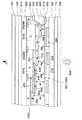
図1は、本実施形態に係るLCDとして、半透過型アクティブマトリクスLCDを用いた場合の概略断面構成を示している。なお、この図1および以降の説明に用いる各図は、本実施形態の構成をより理解しやすいように模式的に示したものであり、寸法は現実のものとは異なっている。本実施形態に係る半透過型LCDは、複数の画素を備え、互いの対向面側に第1電極200、第2電極320が形成された第1及び第2基板100,300を、間に液晶層400を挟んで貼り合わせて構成される。さらに、各画素領域内には透過領域210と反射領域220とが形成されている。 FIG. 1 shows a schematic cross-sectional configuration when a transflective active matrix LCD is used as the LCD according to the present embodiment. Note that FIG. 1 and the drawings used in the following description are schematically shown so that the configuration of the present embodiment can be more easily understood, and the dimensions are different from actual ones. The transflective LCD according to the present embodiment includes a plurality of pixels, and a first and
液晶層400としては負の誘電率異方性を備えた垂直配向型の液晶が採用され、かつ、1画素領域内を複数の配向領域に分割するための配向制御部500(配向分割部)が第2基板側又は第1基板に設けられている。配向制御部500は、例えば図1に示すような液晶層400に向かって突出する突起部510、傾斜部520や、図1では、画素電極200の間隙によって構成される電極不在部などによって構成している(詳しくは後述する)。 As the
第1及び第2基板100,300には、ガラスなどの透明基板が用いられている。第1基板100側には、第1電極として、画素ごとに個別のパターンのITO(Indium Tin Oxide)、IZO(Indium Zinc Oxide)などの透明導電性金属酸化物が用いられた画素電極200及び、この画素電極200に接続された薄膜トランジスタなどのスイッチ素子が形成されている(図示せず)。第1基板100の全面には、画素電極200を覆うように垂直配向型の配向膜260が形成されている。この配向膜260には、例えばポリイミドなどが用いられ、本実施形態では、ラビングレスタイプを採用しており、液晶の初期配向(電圧非印加状態での配向)を膜の平面方向に対して垂直なものとしている。なお、1つの画素電極200の形成領域内に、上記透明の電極のみからなる透明領域210と、上記透明電極と積層形成された反射膜又は反射電極の形成された反射領域220が設けることができる。 Transparent substrates such as glass are used for the first and
このような第1基板100と、液晶層400を挟んで対向する第2基板300には、その液晶層側の面に、まずR(赤),G(緑),B(青)の色フィルタ330r,330g,330bが対応する所定位置に形成されている。各色フィルタ330r,330g,330bの境界部分には、画素間での光漏れを防ぐための遮光層(ここでは黒色色フィルタ)330BMが設けられている。図示するように、色フィルタの厚さは、色ごとに異なり、これにより色ごとの画素の液晶層の厚さを変え、電極間に印加する電圧と透過光量の波長依存性を補償している。したがって、色フィルタ330r,330g,330bは、色に対応して液晶層の厚さ(セルギャップ)を調整する色対応ギャップ調整層として機能する。 In the
色フィルタ330r,330g,330bの上には、各画素の反射領域220に対向する領域においてその液晶層の厚さ(セルギャップ)dr を透過領域210での液晶層の厚さ(セルギャップ)dt より小さい所望の値(dr <dt )とするために、光透過性材料よりなる反射領域ギャップ調整層340が形成されている。また、前述のように色ごとにセルギャップは異なっており、各色の画素の反射領域、透過領域のセルギャップは、必要に応じて前述のdr ,dt に色に対応した添え字r ,g ,b を付して説明する。例えばR用画素の反射領域、透過領域のセルギャップは、それぞれdrr,dtrと表す。なお、この反射領域ギャップ調整層340の厚さは、入射光が液晶層400を1回通過する透過領域210と、2回通過する反射領域220とで、それぞれ最適な透過率、反射率を得るために要求される液晶層の厚さdが異なる場合に対応している。よって、例えば、反射領域ギャップ調整層340を設けない透過領域210で最適な透過率が得られるように液晶層の厚さdを決め、反射領域220では、所望の厚さの反射領域ギャップ調整層340を形成することで、透過領域210よりも小さい液晶層の厚さdを得ることができる。 On the
上記反射領域ギャップ調整層340を含む第2基板300の全面を覆うように、第2電極として、各画素に対して共通の電極(共通電極)320が形成されている。この共通電極320は、上記画素電極200と同様に、ITOやIZOなどの透明導電性金属酸化物を用いて形成することができる。 A common electrode (common electrode) 320 is formed as a second electrode so as to cover the entire surface of the
この共通電極320の上に、本実施形態では、1画素領域内において液晶の配向方向を分割して配向方向の異なる領域を複数形成する配向制御部500として突起部510を形成している。この突起部510は、液晶層400に向かって突起しており、導電性であっても絶縁性であっても良いが、ここでは、絶縁性の例えばアクリル系の樹脂などを所望パターンに形成して形成することができる。また、突起部510は、各画素領域内の透過領域210にも、反射領域220にもそれぞれ形成されている。 In this embodiment, the
上記突起部510及び共通電極320を覆って、第1基板側と同様の垂直配向型、ラビングレスの配向膜262が形成されている。上述のように配向膜262は、その膜平面方向に対して垂直な方向に液晶を配向させるが、突起部510を覆う位置では、突起部510の形状を反映した斜面が形成される。したがって、突起部510の形成位置では、これを覆う配向膜262の斜面に対し、液晶が垂直な方向に配向されることとなり、この突起部510を境に液晶の配向方向が分割される。また、本実施形態では、第2基板側に設けられた上記反射領域ギャップ調整層340の側面をテーパ形状として傾斜させ、この斜面の上方を覆う配向膜262にも斜面を形成し、この斜面においても、液晶が斜面に垂直な方向に制御され、配向制御部500として機能している。 A vertical alignment type
図1に示す半透過型LCDにおいて、第1基板100の外側(光源600側)には直線偏光板(第1偏光板)120、位相差板(第1位相差板)110が設けられている。第1位相差板110は、2種類の位相差板、すなわち1/4波長板(第1λ/4板)と1/2波長板(第1λ/2板)からなる。 In the transflective LCD shown in FIG. 1, a linearly polarizing plate (first polarizing plate) 120 and a retardation plate (first retardation plate) 110 are provided outside the first substrate 100 (on the
第2基板300の外側(観察側)には、負の屈折率異方性を有する光学補償板310が設けられ、さらに、第2位相差板130、直線偏光板である第2偏光板140が設けられている。第2位相差板130も第1位相差板110と同様、1/4,1/2波長板の2種類の位相差板からなる。 An
これらの位相差板110,130および直線偏光板120,140は、まず基板100,300に位相差板が貼着し、更に直線偏光板を貼着するようにもでき、また位相差板と直線偏光板を一体に形成して、その後基板に貼着するようにすることもできる。 The
図2には、第1および第2偏光板120,140、第1および第2位相差板110,130の関係が示されている。なお、符号410で示す部材は、液晶層400とこれを狭持する第1および第2基板100,300、さらにこの基板上に形成された電極、配向膜などからなる液晶セルである。 FIG. 2 shows the relationship between the first and second
第1位相差板110は、液晶セル410側に位置する第1λ/4板112と、第1偏光板120側に位置する第1λ/2板114がはり合わされて構成される。第2位相差板130も、液晶セル410側に位置する第2λ/4板132と、第2偏光板140側に位置する第2λ/2板134がはり合わされて構成される。 The
第1及び第2λ/4板112,132は、それぞれの複屈折光に対し、138±10μmの位相差を生じさせ、第1及び第2λ/2板114,134は、275±10μmの位相差を生じさせる。したがって、これらの位相差板は、550nmの波長に対し、1/4波長板、1/2波長板となっている。また、偏光板の吸収軸、位相差板の遅相軸の配置は、第2偏光板140の吸収軸141の向きを0°としたときに、次のようになっている。第2λ/2板134の遅相軸135が15°、第2λ/4板132の遅相軸133が75°、第1λ/4板112の遅相軸113が165°、第1λ/2板114の遅相軸115が遅相軸105°、そして第1偏光板の吸収軸121が90°となるようにそれぞれが配置されている。第1λ/4板の遅相軸113と第1λ/2板の遅相軸115は、第1偏光板の吸収軸121を基準とすれば、それぞれ15°,75°の配置となっていることが分かる。 The first and second λ / 4
図3および図4は、一つのλ/4板またはλ/2板が生じさせる位相差を、それぞれ275,138μmを中心に振ったときのコントラストを示している。要求されるコントラスト300以上を達成するには、λ/4板において±10μmの範囲とする必要がある。λ/2板については、より広い範囲とすることが可能であるが、λ/4板にあわせて±10μmとする。 3 and 4 show the contrast when the phase difference generated by one λ / 4 plate or λ / 2 plate is swung around 275 and 138 μm, respectively. In order to achieve the required contrast of 300 or more, it is necessary to set the range of ± 10 μm in the λ / 4 plate. The λ / 2 plate can be in a wider range, but is set to ± 10 μm in accordance with the λ / 4 plate.
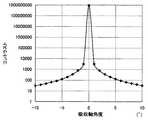
図5から図7は、第2偏光板の吸収軸の角度、第2λ/2板、第2λ/4板の遅相軸の角度をそれぞれ0°,15°,75°を中心に振ったときのコントラストを示している。コントラスト300を得るには偏光板、λ/4板では±3°の範囲とすることが必要である。λ/2板においては±2°とする必要があるが、公差の端、すなわち+3°、−3°付近の出現率は低いことを考えて、他の板とあわせて±3°とする。第1偏光板、第1λ/2板、第1λ/4板については、対称性から同一の範囲とすればよい。 FIGS. 5 to 7 show the case where the absorption axis angle of the second polarizing plate and the slow axis angles of the second λ / 2 plate and the second λ / 4 plate are swung around 0 °, 15 °, and 75 °, respectively. The contrast is shown. In order to obtain the
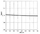
図8は、λ/2板とλ/4板を、前述の角度で組み合わせた位相差板の位相差の、波長依存性を示すグラフである。図から理解されるように、可視領域においてほぼ均一な位相差を生じさせることができる。 FIG. 8 is a graph showing the wavelength dependence of the retardation of a retardation plate in which a λ / 2 plate and a λ / 4 plate are combined at the aforementioned angles. As understood from the figure, a substantially uniform phase difference can be generated in the visible region.
光源600から射出され光は、第1基板100側の直線偏光板120を透過し偏光板120の偏光軸に沿った方向(吸収軸に直交する方向)に直線偏光する。この直線偏光は、第1位相差板110においてその位相差が円偏光となる。ここで、本実施形態では、少なくとも波長の異なるR,G,Bのいずれの成分に対しても確実に円偏光として、液晶セルでの光の利用効率(透過率)を高めるために、λ/4板、λ/2板を組み合わせて広帯域円偏光板としている。得られた円偏光は、透過領域210において画素電極200を透過して液晶層400に入射する。 Light emitted from the
本実施形態に係る半透過型LCDでは、液晶層400には、上述のように、負の誘電率異方性(Δε<0)をもつ垂直配向型液晶を用いており、また垂直配向型の配向膜260,262を用いている。 In the transflective LCD according to the present embodiment, as described above, the
よって、電圧非印加状態では、配向膜260,262の形成する平面の法線方向に配向し、印加電圧が大きくなるにつれ、液晶の長軸方向が画素電極200と共通電極320の間に形成される電界に対して直交方向(基板の平面方向に平行)へと傾く。液晶層400に電圧が印加されていない場合には、液晶層400で偏光状態が変化せず、円偏光のまま第2基板300に到達し、第2位相差板130で円偏光が解消され、直線偏光となる。このとき第2位相差板130の直線偏光の方向と直交するように第2偏光板140が配置してあるので、この直線偏光は、第1偏光板120と直交方向の透過軸(偏光軸)の第2偏光板140を透過することができず、表示は黒となる。 Therefore, in the voltage non-applied state, the liquid crystal is oriented in the normal direction of the plane formed by the
液晶層400に電圧が印加されると、入射された円偏光に対して液晶層400が位相差を発生させ、例えば逆回りの円偏光や、楕円偏光、直線偏光となり、得られた光に対して第2位相差板130で更にλ/4位相がずらされることで、直線偏光(第2偏光板の透過軸と平行)、楕円偏光や円偏光となり、これらの偏光は第2偏光板140の偏光軸に沿った成分を有しており、その成分に応じた量の光がこの第2偏光板140から観察側に向けて射出させ、表示(白又は中間調)として認識される。 When a voltage is applied to the
なお、光学補償板310は、ネガティブリターダであり、液晶層の中央領域と配向膜260,262との微妙な配向状態の違いを補償する逆の光学異方性を持ち、この位相差板310を透過することで、色つきが解消され、また意図しないプレチルト(配向膜260,262付近での液晶の吸着による固定化等による)などによる表示の反転や色つきなどを解消でき、結果として視野角を向上させることを可能としている。 The
110 第1位相差板、112 第1λ/4板、114 第1λ/2板、120 第1偏光板、130 第2位相差板、132 第2λ/4板、134 第2λ/2板、140 第2偏光板、400 液晶層、410 液晶セル。
110 1st retardation plate, 112 1st λ / 4 plate, 114 1st λ / 2 plate, 120 1st polarizing plate, 130 2nd retardation plate, 132 2nd λ / 4 plate, 134 2nd λ / 2 plate, 140 1st 2 polarizing plates, 400 liquid crystal layers, 410 liquid crystal cells.
Claims (2)
Translated fromJapanese液晶層を狭持する一対の基板のそれぞれには位相差板が貼着され、さらにそれぞれの位相差板上に吸収軸が互いに略90°となるように偏光板が隣接配置され、
前記それぞれ位相差板は、その位相差板に隣接配置された偏光板の吸収軸に対し、遅相軸が略15°傾いた1/2波長板と、遅相軸が略75°傾いた1/4波長板とを有する、
ことを特徴とする液晶表示装置。A liquid crystal display device having a reflective region and a transmissive region in one pixel and having a vertical alignment type liquid crystal layer,
A retardation plate is attached to each of the pair of substrates sandwiching the liquid crystal layer, and polarizing plates are arranged adjacent to each other so that the absorption axes are approximately 90 ° to each other,
Each of the retardation plates is a half-wave plate whose slow axis is inclined by about 15 ° with respect to the absorption axis of the polarizing plate arranged adjacent to the retardation plate, and 1 whose slow axis is inclined by about 75 °. / 4 wavelength plate,
A liquid crystal display device characterized by the above.
液晶層を狭持する一対の基板のそれぞれには位相差板が貼着され、さらにそれぞれの位相差板上に吸収軸が互いに略90°となるように偏光板が隣接配置され、
前記それぞれ位相差板は、その位相差板に隣接配置された偏光板の吸収軸に対し、遅相軸が15±3°傾いた1/2波長板と、遅相軸が75±3°傾いた1/4波長板とを有する、
ことを特徴とする液晶表示装置。
A liquid crystal display device having a reflective region and a transmissive region in one pixel and having a vertical alignment type liquid crystal layer,
A retardation plate is attached to each of the pair of substrates sandwiching the liquid crystal layer, and polarizing plates are arranged adjacent to each other so that the absorption axes are approximately 90 ° to each other,
Each of the retardation plates is a half-wave plate with a slow axis inclined by 15 ± 3 ° and a slow axis of 75 ± 3 ° with respect to the absorption axis of a polarizing plate disposed adjacent to the retardation plate. A quarter-wave plate
A liquid crystal display device characterized by the above.
Priority Applications (1)
| Application Number | Priority Date | Filing Date | Title |
|---|---|---|---|
| JP2004342894AJP2006154129A (en) | 2004-11-26 | 2004-11-26 | Liquid crystal display device |
Applications Claiming Priority (1)
| Application Number | Priority Date | Filing Date | Title |
|---|---|---|---|
| JP2004342894AJP2006154129A (en) | 2004-11-26 | 2004-11-26 | Liquid crystal display device |
Publications (1)
| Publication Number | Publication Date |
|---|---|
| JP2006154129Atrue JP2006154129A (en) | 2006-06-15 |
Family
ID=36632543
Family Applications (1)
| Application Number | Title | Priority Date | Filing Date |
|---|---|---|---|
| JP2004342894APendingJP2006154129A (en) | 2004-11-26 | 2004-11-26 | Liquid crystal display device |
Country Status (1)
| Country | Link |
|---|---|
| JP (1) | JP2006154129A (en) |
Cited By (3)
| Publication number | Priority date | Publication date | Assignee | Title |
|---|---|---|---|---|
| JP2009300709A (en)* | 2008-06-13 | 2009-12-24 | Sony Corp | Image display device and method for adjusting the same |
| KR20120066288A (en)* | 2010-12-14 | 2012-06-22 | 엘지디스플레이 주식회사 | Liquid crystal display device and method of manfacturing the same |
| KR20160078635A (en)* | 2014-12-24 | 2016-07-05 | 엘지디스플레이 주식회사 | Trans-flective mode liquidcrystal display device |
- 2004
- 2004-11-26JPJP2004342894Apatent/JP2006154129A/enactivePending
Cited By (5)
| Publication number | Priority date | Publication date | Assignee | Title |
|---|---|---|---|---|
| JP2009300709A (en)* | 2008-06-13 | 2009-12-24 | Sony Corp | Image display device and method for adjusting the same |
| KR20120066288A (en)* | 2010-12-14 | 2012-06-22 | 엘지디스플레이 주식회사 | Liquid crystal display device and method of manfacturing the same |
| KR101876567B1 (en)* | 2010-12-14 | 2018-08-02 | 엘지디스플레이 주식회사 | Liquid crystal display device and method of manfacturing the same |
| KR20160078635A (en)* | 2014-12-24 | 2016-07-05 | 엘지디스플레이 주식회사 | Trans-flective mode liquidcrystal display device |
| KR102224092B1 (en)* | 2014-12-24 | 2021-03-08 | 엘지디스플레이 주식회사 | Trans-flective mode liquidcrystal display device |
Similar Documents
| Publication | Publication Date | Title |
|---|---|---|
| US11874576B2 (en) | Optical stack for privacy display | |
| KR101299575B1 (en) | Transflective liquid crystal displays, manufacturing method thereof, and computer | |
| US8405806B2 (en) | Liquid crystal display device that includes both a transmissive portion and a reflective portion | |
| KR100439354B1 (en) | Transflective LCD | |
| JP5252335B2 (en) | Liquid crystal display device and terminal device | |
| US20120120328A1 (en) | Transflective Liquid Crystal Displays Using Transverse Electric Field Effect | |
| JP2006098861A (en) | Liquid crystal display apparatus | |
| KR20110037001A (en) | Polarizing plate and display device having same | |
| US20070126963A1 (en) | Transflective liquid crystal display device | |
| JP2006098870A (en) | Liquid crystal display | |
| US7443473B2 (en) | Optical compensation polarizing film achieving a higher viewing angle | |
| KR101915923B1 (en) | Liquid crystal display device and head-up display device | |
| JP2006154129A (en) | Liquid crystal display device | |
| JP2004151714A (en) | Liquid crystal display | |
| JP2005196043A (en) | Liquid crystal display element | |
| JP4824443B2 (en) | Liquid crystal display | |
| JP4846231B2 (en) | Liquid crystal display | |
| CN113514984A (en) | Liquid crystal display panel, method for producing the same, and display device | |
| KR101138262B1 (en) | Transflective LCD | |
| JP2003149636A (en) | Liquid crystal display device | |
| KR100683137B1 (en) | Reflective Fringe Field Drive Mode Liquid Crystal Display | |
| JP2011112927A (en) | Liquid crystal display | |
| JP4985798B2 (en) | Liquid crystal display element | |
| JP2023179938A (en) | Optical elements and display devices | |
| KR20070002791A (en) | Transverse electric field reflection type liquid crystal display device |