JP2006147889A - Surface mount type LED - Google Patents
Surface mount type LEDDownload PDFInfo
- Publication number
- JP2006147889A JP2006147889AJP2004336708AJP2004336708AJP2006147889AJP 2006147889 AJP2006147889 AJP 2006147889AJP 2004336708 AJP2004336708 AJP 2004336708AJP 2004336708 AJP2004336708 AJP 2004336708AJP 2006147889 AJP2006147889 AJP 2006147889A
- Authority
- JP
- Japan
- Prior art keywords
- substrate
- chip
- led
- conductive layer
- mounting
- Prior art date
- Legal status (The legal status is an assumption and is not a legal conclusion. Google has not performed a legal analysis and makes no representation as to the accuracy of the status listed.)
- Pending
Links
Images


Classifications
- H—ELECTRICITY
- H01—ELECTRIC ELEMENTS
- H01L—SEMICONDUCTOR DEVICES NOT COVERED BY CLASS H10
- H01L2224/00—Indexing scheme for arrangements for connecting or disconnecting semiconductor or solid-state bodies and methods related thereto as covered by H01L24/00
- H01L2224/01—Means for bonding being attached to, or being formed on, the surface to be connected, e.g. chip-to-package, die-attach, "first-level" interconnects; Manufacturing methods related thereto
- H01L2224/42—Wire connectors; Manufacturing methods related thereto
- H01L2224/47—Structure, shape, material or disposition of the wire connectors after the connecting process
- H01L2224/48—Structure, shape, material or disposition of the wire connectors after the connecting process of an individual wire connector
- H01L2224/4805—Shape
- H01L2224/4809—Loop shape
- H01L2224/48091—Arched
Landscapes
- Led Device Packages (AREA)
Abstract
Translated fromJapaneseDescription
Translated fromJapanese本発明は、チップ基板から成る表面実装型LEDに関するものである。 The present invention relates to a surface-mounted LED comprising a chip substrate.
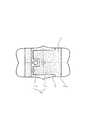
従来、表面実装型LED1は、例えば図11に示すように、構成されている。 図11において、表面実装型LED1は、チップ基板2と、チップ基板2上に搭載されたLEDチップ3と、LEDチップ3を包囲するようにチップ基板2上に形成された枠状部材4と、枠状部材4の凹陥部4a内に充填されたモールド樹脂5と、から構成されている。 Conventionally, the surface-mounted
上記チップ基板2は、平坦な銅張り配線基板として耐熱性樹脂から構成されており、その表面にチップ実装ランド2a,接続ランド2bと、これらから両端縁を介して下面に回り込む表面実装用端子部2c,2dと、を備えている。
そして、チップ基板2のチップ実装ランド2a上に、LEDチップ3が接合されると共に、隣接する接続ランド2bに対してワイヤボンディングにより電気的に接続されるようになっている。The
The LED chip 3 is bonded onto the chip mounting land 2a of the
上記枠状部材4は、同様に耐熱性樹脂によりチップ基板2上に形成されると共に、LEDチップ3の周りを包囲するように逆円錐台状の凹陥部4aを備えている。尚、この凹陥部4aの内面は、好ましくは反射面として構成されている。 The frame-
このような構成の表面実装型LED1によれば、表面実装用端子2c,2dを介してLEDチップ3に駆動電圧が印加されると、LEDチップ3が発光し、この光が直接にまたは凹陥部4aの内面で反射されて上方から外部に出射されることになる。 According to the surface-mounted
しかしながら、このような構成の表面実装型LED1においては、以下のような問題がある。
即ち、表面実装型LED1においては、図12に示すように、チップ基板2の表面に、第一の導電層として、チップ実装ランド2a及び接続ランド2bが形成されていると共に、図13に示すように、チップ基板2の裏面に、第二の導電層として、表面実装用端子2c,2dが形成されている。
そして、表面実装型LED1の駆動発光時に、LEDチップ3で発生する熱は、チップ実装ランド2aからチップ基板2の側面から裏面に回り込む表面実装用端子2cを介して、第二の導電層に放熱されるようになっている。However, the surface-mounted
That is, in the surface-mounted
The heat generated in the LED chip 3 during driving light emission of the surface-mounted
これは、チップ基板2自体が樹脂等から構成されており、導電層を構成する金属、例えば銅(熱伝導率約390W/mK)と比較して、熱伝導率が大幅に低い(例えば熱伝導率約0.2W/mK)ために、LEDチップ3からの熱が上記チップ実装ランド2aから隣接する狭い連結部分2eを通って表面実装用端子2cに対して放熱されることになるためである。
このため、LEDチップ3の放熱が十分に行なわれないことがあり、LEDチップ3の温度が上昇すると、LEDチップ3の発光効率が低下し、信頼性が低下することになる。This is because the
For this reason, the heat dissipation of the LED chip 3 may not be sufficiently performed, and when the temperature of the LED chip 3 rises, the light emission efficiency of the LED chip 3 decreases and the reliability decreases.
本発明は、以上の点から、簡単な構成により、LEDチップからの熱が効率的に放熱され得るようにした表面実装型LEDを提供することを目的としている。 In view of the above, an object of the present invention is to provide a surface-mounted LED that can efficiently dissipate heat from an LED chip with a simple configuration.
上記目的は、本発明によれば、チップ基板と、このチップ基板の上面にて互いに対向するように形成されると共に、チップ基板の裏面まで回り込んで表面実装用端子を画成する導電パターンから成る一対の電極部材と、一方の電極部材の先端に設けられたチップ実装部上に接合されると共に、他方の電極部材の接続部に対して電気的に接続されたLEDチップと、を含んでいる表面実装型LEDであって、上記チップ基板が多層基板として構成されており、上記チップ基板の最上層の基板表面に形成された第一の導電層が、チップ実装部及び接続部が構成していると共に、最下層の基板裏面に形成された第二の導電層が、表面実装用端子を構成していて、上記チップ基板の最上層の基板裏面,最下層の基板表面そして中間層の基板両面に形成された比較的大面積の他の導電層が、各層を介して、熱伝導を行なうことを特徴とする、表面実装型LEDにより、達成される。 According to the present invention, the above object is based on a chip substrate and a conductive pattern which is formed so as to face each other on the upper surface of the chip substrate and which wraps around to the back surface of the chip substrate to define a surface mounting terminal. A pair of electrode members, and an LED chip bonded to a chip mounting portion provided at the tip of one electrode member and electrically connected to the connection portion of the other electrode member. The chip substrate is configured as a multilayer substrate, and the first conductive layer formed on the uppermost substrate surface of the chip substrate is composed of the chip mounting portion and the connection portion. And the second conductive layer formed on the back surface of the lowermost substrate constitutes a surface mounting terminal, and the uppermost substrate back surface, the lowermost substrate surface, and the intermediate layer substrate of the chip substrate. Form on both sides Another conductive layer having a relatively large area which is, through each layer, and performing heat transfer by surface-mounted LED, it is achieved.
本発明による表面実装型LEDは、好ましくは、上記最上層の基板ができるだけ薄く形成されている。 In the surface-mounted LED according to the present invention, the uppermost substrate is preferably formed as thin as possible.
本発明による表面実装型LEDは、好ましくは、上記最上層の基板のチップ実装部が、実装されるLEDチップの底面積と比較して十分に大きく形成されている。 In the surface-mounted LED according to the present invention, the chip mounting portion of the uppermost substrate is preferably formed sufficiently larger than the bottom area of the LED chip to be mounted.
本発明による表面実装型LEDは、好ましくは、上記最上層の基板のチップ実装部が、この最上層の基板の裏面の導電層と導通している。 In the surface-mounted LED according to the present invention, the chip mounting portion of the uppermost substrate is preferably electrically connected to the conductive layer on the back surface of the uppermost substrate.
上記構成によれば、一対の電極部材を介してLEDチップに駆動電圧が印加されることにより、LEDチップが光を出射する。
この場合、チップ基板が多層基板として構成されており、各基板の間にて、互いに対向する個々の基板の双方に形成された比較的断面積の導電層が互いに接触することになる。これにより、LEDチップからの熱が第一の導電層により吸収され、個々の基板を介してその下に位置する基板境界の導電層に順次に伝達され、最下層の基板の裏面に形成された第二の導電層まで伝達され、実装基板に対して放熱され得ることになる。According to the above configuration, the LED chip emits light when a driving voltage is applied to the LED chip via the pair of electrode members.
In this case, the chip substrate is configured as a multilayer substrate, and conductive layers having relatively cross-sectional areas formed on both of the individual substrates facing each other are in contact with each other between the substrates. As a result, heat from the LED chip is absorbed by the first conductive layer, and is sequentially transmitted to the conductive layer at the substrate boundary located thereunder through the individual substrates, and is formed on the back surface of the lowermost substrate. It is transmitted to the second conductive layer and can be radiated to the mounting substrate.
ここで、個々の基板の間の両面に形成された導電層が比較的断面積であると共に、個々の基板の厚さは従来のチップ基板と比較して薄いことから、個々の基板を構成する樹脂等の熱伝導率が比較的低くても、最上層の基板から中間の基板を介して最下層の基板まで、それらの間に配置された比較的大面積の導電層を介して、熱が効率良く伝達され得ることになる。
従って、LEDチップからの熱が効率良く放熱されることになり、LEDチップの温度上昇が効果的に抑制されるので、発光効率が低下するようなことはなく、信頼性が向上する。
また、LEDチップに対してより大きな電流を流すことが可能になるため、高輝度化を図ることも可能となる。Here, the conductive layers formed on both surfaces between the individual substrates have a relatively cross-sectional area, and the thickness of each of the substrates is smaller than that of the conventional chip substrate. Even if the thermal conductivity of the resin or the like is relatively low, heat is transferred from the uppermost substrate through the intermediate substrate to the lowermost substrate through a relatively large conductive layer disposed between them. It can be transmitted efficiently.
Therefore, the heat from the LED chip is efficiently radiated and the temperature rise of the LED chip is effectively suppressed, so that the light emission efficiency is not lowered and the reliability is improved.
In addition, since a larger current can be supplied to the LED chip, it is possible to increase the luminance.
上記最上層の基板ができるだけ薄く形成されている場合には、LEDチップから第一の導電層に伝達された熱が、最上層の基板を介して効率良くその裏面に形成された導電層に伝達され得ることになる。 When the uppermost substrate is formed as thin as possible, the heat transferred from the LED chip to the first conductive layer is efficiently transferred to the conductive layer formed on the back surface through the uppermost substrate. Will be able to.
上記最上層の基板のチップ実装部が、実装されるLEDチップの底面積と比較して十分に大きく形成されている場合には、LEDチップからの熱がチップ実装部を介して効率良く第一の導電層に伝達され得ることになる。 When the chip mounting portion of the uppermost substrate is formed sufficiently larger than the bottom area of the LED chip to be mounted, the heat from the LED chip is efficiently first through the chip mounting portion. Can be transmitted to the conductive layer.
上記最上層の基板のチップ実装部が、この最上層の基板の裏面の導電層と導通している場合には、LEDチップからの熱が、最上層の基板表面の第一の導電層から直接にその裏面の導電層に効率良く伝達され得ることになる。 When the chip mounting portion of the uppermost substrate is electrically connected to the conductive layer on the back surface of the uppermost substrate, the heat from the LED chip is directly from the first conductive layer on the uppermost substrate surface. Therefore, it can be efficiently transmitted to the conductive layer on the back surface.
このようにして、本発明によれば、チップ基板を多層基板として、個々の基板の間に比較的大面積の放熱効果を有する導電層を形成することにより、最上層の基板上に形成された第一の導電層のチップ実装部に実装されたLEDチップから駆動の際に発生する熱が、個々の基板を介して各導電層を順次に伝達される。これにより、LEDチップからの熱が、効率良く放熱されることになり、LEDチップの温度上昇が抑制され、LEDチップの発光効率の低下が抑制され得ることになる。 In this way, according to the present invention, the chip substrate is formed on the uppermost substrate by forming a conductive layer having a relatively large area of heat dissipation between the individual substrates using a multilayer substrate. Heat generated during driving from the LED chip mounted on the chip mounting portion of the first conductive layer is sequentially transmitted to each conductive layer through the individual substrates. Thereby, the heat from the LED chip is efficiently radiated, the temperature rise of the LED chip is suppressed, and the decrease in the light emission efficiency of the LED chip can be suppressed.
以下、この発明の好適な実施形態を図1乃至図10を参照しながら、詳細に説明する。
尚、以下に述べる実施形態は、本発明の好適な具体例であるから、技術的に好ましい種々の限定が付されているが、本発明の範囲は、以下の説明において特に本発明を限定する旨の記載がない限り、これらの態様に限られるものではない。Hereinafter, preferred embodiments of the present invention will be described in detail with reference to FIGS. 1 to 10.
The embodiments described below are preferable specific examples of the present invention, and thus various technically preferable limitations are given. However, the scope of the present invention particularly limits the present invention in the following description. As long as there is no description of the effect, it is not restricted to these aspects.
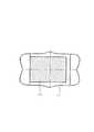
図1は、本発明による表面実装型LEDの第一の実施形態の構成を示している。
図1において、表面実装型LED10は、チップ基板11と、チップ基板11上に搭載されたLEDチップ12と、LEDチップ12を包囲するようにチップ基板11上に形成された枠状部材13と、枠状部材13の凹陥部13a内に充填されたモールド樹脂14と、から構成されている。FIG. 1 shows the configuration of a first embodiment of a surface-mounted LED according to the present invention.
In FIG. 1, the surface-mounted
上記チップ基板11は、平坦な銅張り配線基板として耐熱性樹脂から構成されており、その表面にチップ実装ランド11a,接続ランド11bと、これらから両端縁を介して下面に回り込む表面実装用端子部11c,11dと、を備えている。
そして、チップ基板11のチップ実装ランド11a上に、LEDチップ12が接合されると共に、隣接する接続ランド11bに対してワイヤボンディングにより電気的に接続されるようになっている。The
The
上記枠状部材13は、同様に耐熱性樹脂によりチップ基板11上に形成されると共に、LEDチップ12の周りを包囲するように逆円錐台状の凹陥部13aを備えている。尚、この凹陥部13aの内面は、好ましくは反射面として構成されている。 Similarly, the frame-
以上の構成は、図11に示した従来の表面実装型LED1と同様の構成であるが、本発明実施形態による表面実装型LED10においては、さらに以下のように構成されている点で異なる構成になっている。
即ち、上記チップ基板11は、この場合、二層構造として、上方基板15及び下方基板16から構成されている。The above configuration is the same as that of the conventional surface-mounted
That is, in this case, the
そして、上記上方基板15は、その表面に、図2に示すように、前述したチップ実装ランド11a及び隣接する接続ランド11bを画成する第一の導電層15aを備えていると共に、その裏面には、図3に示すように、比較的大面積の導電層15bをほぼ全面に亘って備えている。
ここで、上記チップ実装ランド11aは、図2に示すように、その面積がLEDチップ12の底面積と比較して十分に大きく選定されており、LEDチップ12からの熱がチップ実装ランド11aに効率良く放熱され得るようになっている。As shown in FIG. 2, the
Here, as shown in FIG. 2, the area of the chip mounting land 11a is selected to be sufficiently larger than the bottom area of the
また、上記下方基板16は、その表面に、図4に示すように、上記導電層15bと同様に、表面全体に亘って形成された比較的大面積の導電層16aを備えていると共に、その裏面には、図5に示すように、前述した表面実装用端子11c,11dを画成する第二の導電層16bを備えている。
そして、上記上方基板15及び下方基板16が互いに重ね合わされることによって、上記導電層15b,16aが互いに密着される。Further, as shown in FIG. 4, the
The
本発明実施形態によるLED10は、以上のように構成されており、表面実装用端子11c,11dを介してLEDチップ12に駆動電圧が印加されると、LEDチップ12が発光し、この光が直接にまたは凹陥部13aの内面で反射されて上方から外部に出射されることになる。
この場合、チップ基板11が二層基板として構成されており、各基板15,16の間にて、互いに対向する個々の基板の双方に形成された比較的断面積の導電層15b,16aが互いに接触することになる。これにより、LEDチップ12からの熱が上方基板15の第一の導電層15aにより吸収され、この上方基板15を介して、その裏面の導電層15bそして導電層16aに伝達され、さらに下方基板16を介して、その裏面に形成された第二の導電層16bもしくは実装基板まで伝達されることになる。
これにより、LEDチップ12からの熱が、効率良く第二の導電層16bまで伝達され、実装基板に対して放熱され得ることになる。従って、LEDチップ12の温度上昇が抑制されることになり、LEDチップ12の発光効率が低下することはなく、表面実装型LED10の信頼性が向上することになる。The
In this case, the
Thereby, the heat from the
発明者等による検討によると、実装ランド11aの面積をS(mm2、図2参照)、実装ランドを画成する第一の導電層15aと、それに最も近い導電層の導電層15bとの間の法線方向の距離をL(mm)としたとき、L/Sが0.2(/mm)以下のときに良好な放熱特性が得られた。これよりも大きい場合には熱抵抗が大きく放熱の効率が悪い。特に熱抵抗がおおよそ1000K/Wを超えると、放熱効果が乏しかった。なお、実装ランドの面積とは、配線部15bも含むLEDを搭載している導電層の基板表面における面積をいう。
具体的には、総面積Sを0.8mm2以上とし、距離Sを0.3mm以内とするとよい。本実施例の場合には熱抵抗が450K/Wであり、背景技術にて説明した従来例に比べておおよそ80%熱抵抗が優れていた。According to the study by the inventors, the area of the mounting land 11a is S (mm2, see FIG. 2), and between the first conductive layer 15a that defines the mounting land and the conductive layer 15b of the closest conductive layer. When the distance in the normal direction was L (mm), good heat dissipation characteristics were obtained when L / S was 0.2 (/ mm) or less. If it is larger than this, the thermal resistance is large and the heat dissipation efficiency is poor. In particular, when the thermal resistance exceeded approximately 1000 K / W, the heat dissipation effect was poor. The area of the mounting land refers to the area of the substrate surface of the conductive layer on which the LED including the wiring portion 15b is mounted.
Specifically, the total area S is preferably 0.8
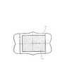
図6は、本発明による表面実装型LEDの第二の実施形態の構成を示している。
図6において、表面実装型LED20は、チップ基板21と、チップ基板21上に搭載されたLEDチップ22と、LEDチップ22を包囲するようにチップ基板21上に形成された枠状部材23と、枠状部材23の凹陥部23a内に充填されたモールド樹脂部24と、から構成されている。FIG. 6 shows the configuration of the second embodiment of the surface-mounted LED according to the present invention.
In FIG. 6, the surface-mounted
尚、上記LEDチップ22,枠状部材23及びモールド樹脂部24は、図1に示したLED10におけるLEDチップ12,枠状部材13及びモールド樹脂部24と同じ構成であるので、その説明を省略する。 The LED chip 22, the frame-shaped
上記チップ基板21は、この場合、三層構造として、上方基板25,中間基板26及び下方基板27から構成されている。 In this case, the
そして、上記上方基板25は、その表面に、図7に示すように、前述したチップ実装ランド21a及び隣接する接続ランド21bを画成する第一の導電層25aを備えていると共に、その裏面には、図8に示すように、比較的大面積の導電層25bをほぼ全面に亘って備えている。この導電層25bは、表面実装用端子22cと接続されている。 As shown in FIG. 7, the
ここで、上記接続ランド21bは、図7に示すように、その面積がチップ実装ランド21aを除く領域にて十分に大きく選定されており、上記導電層25bから上方基板25を介して効率良く放熱され得るようになっている。
さらに、上記上方基板25は、チップ実装ランド21aから上方基板25を上下に貫通して導電層25bに導通する導電パターン25cを備えており、LEDチップ22からの熱が、チップ実装ランド21aから導電パターン25cを介して直接に導電層25bに伝達されるようになっている。Here, as shown in FIG. 7, the area of the connection land 21b is selected to be sufficiently large in a region excluding the chip mounting land 21a, and heat is efficiently radiated from the conductive layer 25b through the
Further, the
また、中間基板26は、その裏面に、図9に示すように、比較的大面積の導電層26aをほぼ全面に亘って備えている。この導電層26aは、表面実装用端子22dと接続されている。
さらに、上記下方基板27は、その裏面には、図10に示すように、前述した表面実装用端子21c,21dを画成する第二の導電層27aを備えている。Further, as shown in FIG. 9, the
Further, as shown in FIG. 10, the
このような構成のLED20によれば、表面実装用端子21c,21dを介してLEDチップ22に駆動電圧が印加されると、LEDチップ22が発光し、この光が直接にまたは凹陥部23aの内面で反射されて上方から外部に出射されることになる。 According to the
この場合、チップ基板21が三層基板として構成されており、各基板25,26,27の間にて、比較的断面積の導電層25b,26aが配置されることになる。これにより、LEDチップ22からの熱が導電パターン25cを介して導電層25bに伝達され、この導電層25bから上方基板25,中間基板26を介して、それぞれ第一の導電層25a及び導電層26aに吸収される。
そして、第一の導電層25a及び導電層26aで吸収された熱は、それぞれ表面実装用端子21c及び21dを介して、外部の実装基板に放熱されることになる。
これにより、LEDチップ22からの熱が、効率良く第二の導電層27aまで伝達され、実装基板に放熱され得るので、LEDチップ22の温度上昇が抑制されることになり、LEDチップ22の発光効率が低下することはなく、表面実装型LED20の信頼性が向上することになる。In this case, the
The heat absorbed by the first conductive layer 25a and the conductive layer 26a is radiated to the external mounting substrate via the surface mounting terminals 21c and 21d, respectively.
Thereby, the heat from the LED chip 22 can be efficiently transmitted to the second conductive layer 27a and can be radiated to the mounting substrate, so that the temperature rise of the LED chip 22 is suppressed, and the LED chip 22 emits light. The efficiency does not decrease, and the reliability of the surface-mounted
上述した実施形態においては、チップ基板12,22は、二層または三層に構成されているが、これに限らず、四層以上の多層基板であってもよいことは明らかである。
また、上述した第二の実施形態においては、上方基板25に導電パターン25cが備えられているが、これに限らず、導電パターン25cは省略されてもよい。この場合、LEDチップ22からの熱は、表面実装用端子22cを介して導電層25bに伝達され得る。
さらに、上述した実施形態においては、チップ基板11,21上に枠状部材14,24が形成されているが、これに限らず、枠状部材が省略され、その代わりに、モールド樹脂部が形成されていてもよいことは明らかである。In the embodiment described above, the
In the above-described second embodiment, the
Furthermore, in the above-described embodiment, the frame-
このようにして、本発明によれば、簡単な構成により、LEDチップからの熱が効率的に放熱され得るようにした表面実装型LEDが提供され得る。 Thus, according to the present invention, it is possible to provide a surface-mounted LED that can efficiently dissipate heat from the LED chip with a simple configuration.
10 表面実装型LED
11 チップ基板
11a チップ実装ランド
11b 接続ランド
11c,11d 表面実装用端子部
12 LEDチップ
13 枠状部材
13a 凹陥部
14 モールド樹脂
15 上方基板
15a 第一の導電層
15b 導電層
16 下方基板
16a 導電層
16b 第二の導電層
20 表面実装型LED
21 チップ基板
21a チップ実装ランド
21b 接続ランド
21c,21d 表面実装用端子部
22 LEDチップ
23 枠状部材
23a 凹陥部
24 モールド樹脂
25 上方基板
25a 第一の導電層
25b 導電層
25c 導電パターン
26 中間基板
26a 導電層
27 下方基板
27a 第二の導電層10 Surface-mount LED
11 Chip substrate 11a
21 Chip substrate 21a Chip mounting land 21b Connection land 21c, 21d Surface mounting terminal portion 22
Claims (4)
Translated fromJapanese上記チップ基板が多層基板として構成されており、
上記チップ基板の最上層の基板表面に形成された第一の導電層が、チップ実装部及び接続部が構成していると共に、最下層の基板裏面に形成された第二の導電層が、表面実装用端子を構成していて、
上記チップ基板の最上層の基板裏面,最下層の基板表面そして中間層の基板両面に形成された比較的大面積の他の導電層が、各層を介して、熱伝導を行なうことを特徴とする、表面実装型LED。A pair of electrode members formed of a chip substrate, a conductive pattern that is formed so as to face each other on the upper surface of the chip substrate, and that extends to the back surface of the chip substrate to define a surface mounting terminal, and one electrode An LED chip that is bonded onto a chip mounting portion provided at the tip of the member and electrically connected to the connection portion of the other electrode member,
The chip substrate is configured as a multilayer substrate,
The first conductive layer formed on the uppermost substrate surface of the chip substrate is composed of the chip mounting portion and the connecting portion, and the second conductive layer formed on the lower surface of the lower substrate is the front surface. The mounting terminal is configured,
Another conductive layer having a relatively large area formed on the upper surface of the chip substrate, the lowermost substrate surface, and both surfaces of the intermediate layer performs heat conduction through each layer. , Surface mount LED.
Priority Applications (1)
| Application Number | Priority Date | Filing Date | Title |
|---|---|---|---|
| JP2004336708AJP2006147889A (en) | 2004-11-19 | 2004-11-19 | Surface mount type LED |
Applications Claiming Priority (1)
| Application Number | Priority Date | Filing Date | Title |
|---|---|---|---|
| JP2004336708AJP2006147889A (en) | 2004-11-19 | 2004-11-19 | Surface mount type LED |
Publications (1)
| Publication Number | Publication Date |
|---|---|
| JP2006147889Atrue JP2006147889A (en) | 2006-06-08 |
Family
ID=36627215
Family Applications (1)
| Application Number | Title | Priority Date | Filing Date |
|---|---|---|---|
| JP2004336708APendingJP2006147889A (en) | 2004-11-19 | 2004-11-19 | Surface mount type LED |
Country Status (1)
| Country | Link |
|---|---|
| JP (1) | JP2006147889A (en) |
Cited By (5)
| Publication number | Priority date | Publication date | Assignee | Title |
|---|---|---|---|---|
| JP2008288487A (en)* | 2007-05-21 | 2008-11-27 | Citizen Electronics Co Ltd | Surface-mounted light emitting diode |
| JP2009545863A (en)* | 2006-08-04 | 2009-12-24 | オスラム オプト セミコンダクターズ ゲゼルシャフト ミット ベシュレンクテル ハフツング | Thin film semiconductor component and component combination |
| JP2012119712A (en)* | 2006-10-31 | 2012-06-21 | Cree Inc | Integrated heat spreaders for leds and related assemblies |
| JP2014116411A (en)* | 2012-12-07 | 2014-06-26 | Kyocera Corp | Substrate for mounting light emitting element and light emitting device |
| US9142720B2 (en) | 2007-01-29 | 2015-09-22 | Osram Opto Semiconductors Gmbh | Thin-film light emitting diode chip and method for producing a thin-film light emitting diode chip |
Citations (3)
| Publication number | Priority date | Publication date | Assignee | Title |
|---|---|---|---|---|
| JPH09153679A (en)* | 1995-11-30 | 1997-06-10 | Kyocera Corp | Laminated glass ceramic circuit board |
| JP2004235204A (en)* | 2003-01-28 | 2004-08-19 | Kyocera Corp | Light emitting element storage package and light emitting device |
| JP2006128512A (en)* | 2004-10-29 | 2006-05-18 | Ngk Spark Plug Co Ltd | Ceramic substrate for light emitting element |
- 2004
- 2004-11-19JPJP2004336708Apatent/JP2006147889A/enactivePending
Patent Citations (3)
| Publication number | Priority date | Publication date | Assignee | Title |
|---|---|---|---|---|
| JPH09153679A (en)* | 1995-11-30 | 1997-06-10 | Kyocera Corp | Laminated glass ceramic circuit board |
| JP2004235204A (en)* | 2003-01-28 | 2004-08-19 | Kyocera Corp | Light emitting element storage package and light emitting device |
| JP2006128512A (en)* | 2004-10-29 | 2006-05-18 | Ngk Spark Plug Co Ltd | Ceramic substrate for light emitting element |
Cited By (6)
| Publication number | Priority date | Publication date | Assignee | Title |
|---|---|---|---|---|
| JP2009545863A (en)* | 2006-08-04 | 2009-12-24 | オスラム オプト セミコンダクターズ ゲゼルシャフト ミット ベシュレンクテル ハフツング | Thin film semiconductor component and component combination |
| US8872330B2 (en) | 2006-08-04 | 2014-10-28 | Osram Opto Semiconductors Gmbh | Thin-film semiconductor component and component assembly |
| JP2012119712A (en)* | 2006-10-31 | 2012-06-21 | Cree Inc | Integrated heat spreaders for leds and related assemblies |
| US9142720B2 (en) | 2007-01-29 | 2015-09-22 | Osram Opto Semiconductors Gmbh | Thin-film light emitting diode chip and method for producing a thin-film light emitting diode chip |
| JP2008288487A (en)* | 2007-05-21 | 2008-11-27 | Citizen Electronics Co Ltd | Surface-mounted light emitting diode |
| JP2014116411A (en)* | 2012-12-07 | 2014-06-26 | Kyocera Corp | Substrate for mounting light emitting element and light emitting device |
Similar Documents
| Publication | Publication Date | Title |
|---|---|---|
| JP4450230B2 (en) | Semiconductor device | |
| JP5703523B2 (en) | Light emitting diode package and light emitting diode package module | |
| JP4481277B2 (en) | Light emitting diode package | |
| JP2007281468A (en) | LED package having anodizing insulating layer and manufacturing method thereof | |
| US20070145399A1 (en) | Light emitting diode package | |
| JP2009536453A (en) | Thermal surface mounting of multiple LEDs on a heat sink | |
| JP2011119732A5 (en) | Light emitting diode package and light emitting diode package module | |
| JP2009054801A (en) | Heat radiation member, and light emitting module equipped with the same | |
| JP2012174703A (en) | Led module device, and method of manufacturing the same | |
| JP2008187101A (en) | Semiconductor device and mounting structure of semiconductor device | |
| JP2008172187A (en) | Side light emitting device | |
| JP5745784B2 (en) | Light emitting diode | |
| JP2006147889A (en) | Surface mount type LED | |
| JP4831958B2 (en) | Surface mount type LED | |
| JP2008288487A (en) | Surface-mounted light emitting diode | |
| JP4250171B2 (en) | Ceramic package for light emitting device | |
| JP2011077164A (en) | Semiconductor light-emitting device | |
| JP2006278766A (en) | Mounting structure and mounting method of light emitting element | |
| CN101145592B (en) | High heat dissipation LED device | |
| JP2006237285A (en) | Semiconductor light emitting device | |
| JP4679917B2 (en) | Semiconductor light emitting device | |
| JP4625972B2 (en) | Surface mount type LED | |
| CN116072630A (en) | Semiconductor package, package forming method and electronic device | |
| JP2009158769A (en) | Semiconductor device | |
| JPS63190363A (en) | Power package |
Legal Events
| Date | Code | Title | Description |
|---|---|---|---|
| A621 | Written request for application examination | Free format text:JAPANESE INTERMEDIATE CODE: A621 Effective date:20071106 | |
| RD02 | Notification of acceptance of power of attorney | Free format text:JAPANESE INTERMEDIATE CODE: A7422 Effective date:20100624 | |
| RD04 | Notification of resignation of power of attorney | Free format text:JAPANESE INTERMEDIATE CODE: A7424 Effective date:20100630 | |
| A977 | Report on retrieval | Free format text:JAPANESE INTERMEDIATE CODE: A971007 Effective date:20100720 | |
| A131 | Notification of reasons for refusal | Free format text:JAPANESE INTERMEDIATE CODE: A131 Effective date:20100803 | |
| A02 | Decision of refusal | Free format text:JAPANESE INTERMEDIATE CODE: A02 Effective date:20101130 |