JP2006136029A - Integration memory map controller circuit for optical fiber tranceiver - Google Patents
Integration memory map controller circuit for optical fiber tranceiverDownload PDFInfo
- Publication number
- JP2006136029A JP2006136029AJP2006015985AJP2006015985AJP2006136029AJP 2006136029 AJP2006136029 AJP 2006136029AJP 2006015985 AJP2006015985 AJP 2006015985AJP 2006015985 AJP2006015985 AJP 2006015985AJP 2006136029 AJP2006136029 AJP 2006136029A
- Authority
- JP
- Japan
- Prior art keywords
- memory
- value
- digital
- temperature
- transceiver
- Prior art date
- Legal status (The legal status is an assumption and is not a legal conclusion. Google has not performed a legal analysis and makes no representation as to the accuracy of the status listed.)
- Granted
Links
- 230000010354integrationEffects0.000title1
- 239000013307optical fiberSubstances0.000title1
- 238000006243chemical reactionMethods0.000claimsabstractdescription13
- 238000003491arrayMethods0.000claimsabstract3
- 238000000034methodMethods0.000claimsdescription18
- 230000005693optoelectronicsEffects0.000claimsdescription16
- 230000001186cumulative effectEffects0.000claimsdescription6
- 238000012545processingMethods0.000claimsdescription6
- 238000004891communicationMethods0.000abstractdescription4
- 230000006870functionEffects0.000description29
- 239000000835fiberSubstances0.000description9
- 230000003287optical effectEffects0.000description7
- 238000010586diagramMethods0.000description5
- 230000007246mechanismEffects0.000description4
- 238000012544monitoring processMethods0.000description4
- 230000005540biological transmissionEffects0.000description3
- 238000001514detection methodMethods0.000description3
- 238000013459approachMethods0.000description2
- 230000001419dependent effectEffects0.000description2
- 238000004519manufacturing processMethods0.000description2
- 238000005259measurementMethods0.000description2
- 230000008569processEffects0.000description2
- 230000002159abnormal effectEffects0.000description1
- 230000004913activationEffects0.000description1
- 230000009286beneficial effectEffects0.000description1
- 238000013461designMethods0.000description1
- 230000009977dual effectEffects0.000description1
- 230000003993interactionEffects0.000description1
- 230000005855radiationEffects0.000description1
- 238000012360testing methodMethods0.000description1
Images


Classifications
- H—ELECTRICITY
- H04—ELECTRIC COMMUNICATION TECHNIQUE
- H04B—TRANSMISSION
- H04B10/00—Transmission systems employing electromagnetic waves other than radio-waves, e.g. infrared, visible or ultraviolet light, or employing corpuscular radiation, e.g. quantum communication
- H04B10/40—Transceivers
- G—PHYSICS
- G01—MEASURING; TESTING
- G01M—TESTING STATIC OR DYNAMIC BALANCE OF MACHINES OR STRUCTURES; TESTING OF STRUCTURES OR APPARATUS, NOT OTHERWISE PROVIDED FOR
- G01M11/00—Testing of optical apparatus; Testing structures by optical methods not otherwise provided for
- G—PHYSICS
- G01—MEASURING; TESTING
- G01M—TESTING STATIC OR DYNAMIC BALANCE OF MACHINES OR STRUCTURES; TESTING OF STRUCTURES OR APPARATUS, NOT OTHERWISE PROVIDED FOR
- G01M11/00—Testing of optical apparatus; Testing structures by optical methods not otherwise provided for
- G01M11/30—Testing of optical devices, constituted by fibre optics or optical waveguides
- G—PHYSICS
- G01—MEASURING; TESTING
- G01M—TESTING STATIC OR DYNAMIC BALANCE OF MACHINES OR STRUCTURES; TESTING OF STRUCTURES OR APPARATUS, NOT OTHERWISE PROVIDED FOR
- G01M99/00—Subject matter not provided for in other groups of this subclass
- G01M99/002—Thermal testing
- H—ELECTRICITY
- H04—ELECTRIC COMMUNICATION TECHNIQUE
- H04B—TRANSMISSION
- H04B10/00—Transmission systems employing electromagnetic waves other than radio-waves, e.g. infrared, visible or ultraviolet light, or employing corpuscular radiation, e.g. quantum communication
- H04B10/07—Arrangements for monitoring or testing transmission systems; Arrangements for fault measurement of transmission systems
- H04B10/075—Arrangements for monitoring or testing transmission systems; Arrangements for fault measurement of transmission systems using an in-service signal
- H04B10/079—Arrangements for monitoring or testing transmission systems; Arrangements for fault measurement of transmission systems using an in-service signal using measurements of the data signal
- H04B10/0799—Monitoring line transmitter or line receiver equipment
- H—ELECTRICITY
- H04—ELECTRIC COMMUNICATION TECHNIQUE
- H04B—TRANSMISSION
- H04B2210/00—Indexing scheme relating to optical transmission systems
- H04B2210/08—Shut-down or eye-safety
Landscapes
- Physics & Mathematics (AREA)
- Electromagnetism (AREA)
- Engineering & Computer Science (AREA)
- Computer Networks & Wireless Communication (AREA)
- Signal Processing (AREA)
- General Physics & Mathematics (AREA)
- Chemical & Material Sciences (AREA)
- Analytical Chemistry (AREA)
- Optics & Photonics (AREA)
- Optical Communication System (AREA)
- Semiconductor Lasers (AREA)
- Input Circuits Of Receivers And Coupling Of Receivers And Audio Equipment (AREA)
- Lock And Its Accessories (AREA)
- Networks Using Active Elements (AREA)
- Selective Calling Equipment (AREA)
- Measuring Pulse, Heart Rate, Blood Pressure Or Blood Flow (AREA)
Abstract
Description
Translated fromJapanese本発明は、一般に光ファイバトランシーバの分野に関し、より詳細には、トランシーバ内で制御、設定、モニタリング、及び、識別作動を達成するために使用される回路に関する。 The present invention relates generally to the field of fiber optic transceivers, and more particularly to circuitry used to achieve control, configuration, monitoring, and identification operations within a transceiver.
光ファイバトランシーバ内の最も基本的な二つの電子回路は、高速のデジタルデータを受け取り、LED又はレーザダイオードを電気的に駆動して同等な光パルスを作り出すレーザ駆動回路、及び、比較的小さな信号を光検出器から取り込み、それらを増幅及び制限して均一な振幅のデジタル電子出力を作り出す受信回路である。これらの基本的な機能に加え、また時にはこれらと併用して、トランシーバ回路によって処理されるべき他のいくつかのタスクがあり、同様にその機能性を向上させるために、トランシーバ回路によって任意選択的に処理されるべきいくつかのタスクがある。これらのタスクには、以下のものが含まれる。ただし、以下のものに限定はされない。 The two most basic electronic circuits in a fiber optic transceiver receive high-speed digital data and electrically drive an LED or laser diode to produce equivalent light pulses, and a relatively small signal. A receiver circuit that captures from a photodetector and amplifies and limits them to produce a digital electronic output of uniform amplitude. In addition to these basic functions, and sometimes in conjunction with them, there are several other tasks that must be handled by the transceiver circuit as well, optionally by the transceiver circuit to improve its functionality. There are several tasks to be handled. These tasks include the following: However, it is not limited to the following.
−設定機能:これらは、レーザダイオードの閾値電流といった構成要素の特性変動を考慮して、一般に工場で部品ごとに行われる必要な調節に関する。
−識別:これは、典型的には「EEPROM(電気的消去可能及びプログラム可能読み出し専用メモリ)」である汎用メモリ、又は他の不揮発性メモリに関する。メモリは、トランシーバの型式、能力、シリアル番号、及び種々の規格との互換性を識別する種々の情報を記憶するために使用されるシリアル通信規格を用いてアクセス可能であることが望ましい。標準的ではないが、サブ構成要素の改訂及び工場試験データなどの追加情報をこのメモリに更に記憶することが望ましいであろう。
−目の安全性及び一般的障害検知:これらの機能は、異常かつ潜在的に危険な作動パラメータを識別し、適切であればこれらをユーザに報告し、及び/又は、レーザの運転停止を実行するために使用される。-Setting functions: these relate to the necessary adjustments that are generally made on a part-by-part basis in the factory, taking into account component characteristic variations such as the threshold current of the laser diode.
Identification: This relates to general purpose memory, or other non-volatile memory, typically “EEPROM (electrically erasable and programmable read only memory)”. The memory is preferably accessible using the serial communication standard used to store the transceiver type, capabilities, serial number, and various information identifying compatibility with the various standards. Although not standard, it may be desirable to further store additional information in this memory, such as subcomponent revisions and factory test data.
O Eye safety and general fault detection: These functions identify abnormal and potentially dangerous operating parameters, report them to the user if appropriate and / or perform laser shutdown Used to do.
更に、多くのトランシーバにおいて、制御回路が以下の追加機能の一部又は全てを実行することが望ましい。
−温度補償機能:例えば、スロープ効率などの重要なレーザ特性において既知の温度変動に対して補償する。
−モニタリング機能:トランシーバの作動特性と環境とに関する様々なパラメータをモニタする。モニタすることが必要と思われるパラメータには、レーザバイアス電流、レーザ出力、受信電力レベル、供給電圧、及び温度が含まれる。理想的には、これらのパラメータは、モニタされてホスト装置に、従ってトランシーバのユーザに対して報告されるか又は利用可能にされるべきである。Further, in many transceivers, it is desirable for the control circuitry to perform some or all of the following additional functions.
Temperature compensation function: compensates for known temperature fluctuations in important laser characteristics such as, for example, slope efficiency.
-Monitoring function: monitors various parameters related to transceiver operating characteristics and environment. Parameters that may need to be monitored include laser bias current, laser power, received power level, supply voltage, and temperature. Ideally, these parameters should be monitored and reported or made available to the host device and thus to the transceiver user.
−電源オン時間:トランシーバの制御回路は、トランシーバが電源オン状態であった総時間を常時追跡し、ホスト装置にこの時間値を報告するか又は利用可能にするのが望ましい。
−マージン処理:「マージン処理」とは、一般的にトランシーバの能動構成要素を駆動するのに使用される制御信号をスケーリングすることにより、エンドユーザが理想の作動条件からの既知のずれにおけるトランシーバの性能を試験することができる機構である。-Power-on time: The transceiver control circuit preferably keeps track of the total time the transceiver has been in the power-on state and reports or makes this time value available to the host device.
Margin processing: “Margin processing” refers to the transceiver's known deviation from ideal operating conditions by scaling the control signals typically used to drive the transceiver's active components. A mechanism that can be tested for performance.
−他のデジタル信号:デジタル入力及び出力の極性及び出力形式に対する様々な要件にトランシーバを適合させるようにホスト装置がトランシーバを設定できるようにすることが望ましい。例えば、デジタル入力は、送信機の使用不可及び速度選択機能のために使用され、一方、出力は、送信機の障害及び信号断(loss of signal)の状況を標示するために使用される。設定値は、一又は二以上の2進入出力信号の極性を決める。いくつかのトランシーバでは、例えばデジタル入力又は出力値と一緒に使用されるスケール係数を指定することにより一又は二以上のデジタル入力又は出力値のスケールを指定するためにこの設定値を使用することが望ましい。 Other digital signals: It is desirable to allow the host device to configure the transceiver to adapt the transceiver to different requirements for the polarity and output format of the digital inputs and outputs. For example, the digital input is used for transmitter disabling and speed selection functions, while the output is used to indicate transmitter failure and loss of signal situations. The set value determines the polarity of one or two or more two approach output signals. Some transceivers may use this setting to specify the scale of one or more digital input or output values, for example by specifying the scale factor used with the digital input or output value. desirable.
殆どのトランシーバにおいては、これらの追加機能は、部分的にはそのコストのために、たとえあったとしてもわずかしか実装されない。これらの機能のいくつかは、例えば、レーザ駆動又は受信回路内にいくつかの機能を含ませることにより(例えば、レーザ駆動回路内のある程度の温度補償)、又は、市販のマイクロコントローラ集積回路を使用して、認識目的の汎用「EEPROM」を使用する個別の回路を使用して実装されてきた。しかし、今日まで、これらの機能全てと、更にここに列挙されていない追加機能とをサポートする一様な装置アーキテクチャをコスト効率よく提供するいかなるトランシーバも存在していない。 In most transceivers, these additional functions are implemented only slightly, if any, due in part to their cost. Some of these functions are, for example, by including some functions in the laser drive or receiver circuit (eg, some temperature compensation in the laser drive circuit) or using a commercially available microcontroller integrated circuit Thus, it has been implemented using a separate circuit that uses a generic "EEPROM" for recognition purposes. To date, however, there are no transceivers that cost-effectively provide a uniform device architecture that supports all of these functions, as well as additional functions not listed here.
本発明の目的は、簡単明瞭なメモリマップアーキテクチャと単純なシリアル通信機構とを使用して、上述の機能性の全て(又は、任意のサブセット)を達成する一般的で柔軟な集積回路を提供することである。
図1は、典型的な従来技術の光ファイバトランシーバの基本的な特性の概略図である。主回路1は、少なくとも、送信受信回路の経路、電源19、及び接地接続18を包含する。受信回路は、一般に、機械的なファイバ端子と、フォトダイオードと、前置増幅器(プリアンプ)回路とを包含する受信光学サブアセンブリ(ROSA)2で構成される。「ROSA」は、次に、「RX+」及び「RX−」ピン17を通じて外部回路に接続された固定出力スイングデジタル信号を生成する機能を有する後置増幅器(ポストアンプ)集積回路4に接続される。ポストアンプ回路はまた、適度な強さの光入力の有無を指示する「信号検知」又は「信号損失」として知られるデジタル出力信号を提供することが多い。「信号検知」出力は、ピン18に出力として提供される。送信回路は、一般に、送信光学サブアセンブリ(TOSA)3とレーザ駆動集積回路5で構成されることになる。「TOSA」は、機械的なファイバ端子、及び、レーザダイオード又はLEDを包含する。レーザ駆動回路は、レーザに対して一般にAC駆動及びDCバイアス電流を提供することになる。AC駆動用の信号入力は、「TX+」及び「TX−」ピン12から得られる。一般に、レーザ駆動回路には、バイアス電流(又は、出力電力)レベル及びレーザに対するAC変調駆動などの特定のパラメータを個別に工場設定する必要がある。通常、これは、可変抵抗器を調節するか、又は工場で選定された抵抗器7及び9(すなわち、工場選定された抵抗値を有する)を取り付けることにより実行される。更に、バイアス電流及び変調の温度補償が必要な場合が多い。この機能は、レーザ駆動集積回路に一体化されるか、又はサーミスタ6及び8のような外部温度感応素子の使用により達成することができる。It is an object of the present invention to provide a general and flexible integrated circuit that achieves all (or any subset) of the above functionality using a simple and clear memory map architecture and a simple serial communication mechanism. That is.
FIG. 1 is a schematic diagram of the basic characteristics of a typical prior art fiber optic transceiver. The main circuit 1 includes at least a transmission / reception circuit path, a
上述の最も基本的な機能に加えて、いくつかのトランシーバのプラットフォーム規格には、更に別の機能性が含まれる。この例には、「GBIC」規格に説明された「TX」使用不可13及び「TX」障害14ピンがある。「GBIC」規格では、「TX」使用不可ピンにより送信機はホスト装置により停止させられ、一方で「TX」障害ピンは、レーザ又は関連するレーザ駆動回路内に存在する何らかの障害条件をホスト装置に指示するものである。この基本的な説明に加え、「GBIC」規格は、リセット作動と他のアクションとを実行するためにこれらの制御がどのように機能し互いに対話するかを説明する一連のタイミング図を含む。この機能性の大部分は、レーザ回路内に障害の条件が存在する時、目に危険な放射レベルを防止することを狙いとしている。これらの機能は、レーザ駆動回路自体か、又は任意選択的の追加の集積回路11に一体化することができる。最後に、「GBIC」規格はまた、「EEPROM」10が、クロック15とデータ16ラインとで構成されたシリアルインタフェース(「EEPROM」製品の「ATMEL AT24C01A」系列のシリアルインタフェースを使用して形成される)を通じて読み出せる標準化されたシリアルID情報を記憶するように要求する。
機械的ファイバ端子の代替として、いくつかの従来技術のトランシーバは、標準的な雄の光ファイバコネクタである光ファイバピグテールを使用する。
全トランシーバ機能の半分だけが実装された光ファイバ送信機又は受信機にも同様の原理が適用されることは明らかである。In addition to the most basic functions described above, some transceiver platform standards include additional functionality. Examples include “TX” unavailable 13 and “TX”
As an alternative to mechanical fiber terminals, some prior art transceivers use fiber optic pigtails, which are standard male fiber optic connectors.
Obviously, the same principle applies to fiber optic transmitters or receivers where only half of the total transceiver function is implemented.
本発明は、好ましくは、レーザ送信機とフォトダイオード受信機とを有するトランシーバを制御するための、時にコントローラと呼ばれる単一チップ集積回路として実施される。このコントローラは、トランシーバに関する情報を記憶するためのメモリと、レーザ送信機及びフォトダイオード受信機から複数のアナログ信号を受信し、受信したアナログ信号をデジタル値に変換し、そのデジタル値をメモリ内の所定の領域に記憶するアナログ/デジタル変換回路を含む。比較論理回路は、限界値と一又は二以上のデジタル値とを比較し、その比較に基づいてフラッグ値を生成し、そのフラッグ値をメモリ内の所定の領域に記憶する。コントローラ内の制御回路は、メモリ内に記憶された一又は二以上の値に従ってレーザ送信機の作動を制御する。シリアルインタフェースは、ホスト装置がメモリ内の領域で読取り及び書込みができるようにするために設けられる。コントローラの複数の制御機能と複数のモニタリング機能とは、ホストコンピュータがコントローラ内の対応するメモリマップ領域にアクセスすることにより実行される。 The present invention is preferably implemented as a single chip integrated circuit, sometimes referred to as a controller, for controlling a transceiver having a laser transmitter and a photodiode receiver. The controller receives a plurality of analog signals from a memory for storing information about the transceiver, a laser transmitter and a photodiode receiver, converts the received analog signals into digital values, and converts the digital values into the memory. An analog / digital conversion circuit that stores data in a predetermined area is included. The comparison logic circuit compares the limit value with one or more digital values, generates a flag value based on the comparison, and stores the flag value in a predetermined area in the memory. A control circuit in the controller controls the operation of the laser transmitter according to one or more values stored in the memory. The serial interface is provided to allow the host device to read and write to areas in the memory. A plurality of control functions and a plurality of monitoring functions of the controller are executed when the host computer accesses a corresponding memory map area in the controller.
いくつかの実施形態では、コントローラは、トランシーバの累積作動時間に相当する時間値を生成するための累積時計を更に含み、その生成された時間値は、シリアルインタフェースを通じて読み込み可能である。
いくつかの実施形態では、コントローラは、トランシーバの電源電圧レベルに対応する電力レベル信号を生成する電源電圧センサを更に含む。これらの実施形態においては、アナログ/デジタル変換回路が構成され、電力レベル信号をデジタル電力レベル値に変換し、デジタル電力レベル値をメモリ内の所定の電力レベルの領域に記憶する。更に、コントローラの比較論理回路は、デジタル電力レベル値を電力(すなわち、電圧)レベル限界値と比較し、デジタル電力レベル信号の電力レベル限界値との比較に基づいてフラッグ値を生成し、電力レベルフラッグ値をメモリ内の所定の電力レベルフラッグ領域に記憶するための論理回路を任意選択で含むことができる。尚,電源電圧センサは、受信された光信号の電力レベルとは別個のトランシーバの電圧供給レベルを計測する。In some embodiments, the controller further includes a cumulative clock for generating a time value corresponding to the cumulative operating time of the transceiver, the generated time value being readable through a serial interface.
In some embodiments, the controller further includes a power supply voltage sensor that generates a power level signal corresponding to the power supply voltage level of the transceiver. In these embodiments, an analog / digital conversion circuit is configured to convert the power level signal to a digital power level value and store the digital power level value in a region of a predetermined power level in the memory. In addition, the comparison logic of the controller compares the digital power level value with the power (ie, voltage) level limit value, generates a flag value based on the comparison with the power level limit value of the digital power level signal, and A logic circuit may optionally be included to store the flag value in a predetermined power level flag area in the memory. The power supply voltage sensor measures the voltage supply level of the transceiver that is separate from the power level of the received optical signal.
いくつかの実施形態では、コントローラは、トランシーバの温度に対応する温度信号を生成する温度センサを更に含む。これらの実施形態では、アナログ/デジタル変換回路が構成されて温度信号をデジタル温度値に変換し、デジタル温度値をメモリ内の所定の温度の領域に記憶する。更に、コントローラの比較論理回路は、デジタル温度値を温度限界値と比較するための論理回路を任意選択で含み、デジタル温度信号と温度限界値との比較に基づいてフラッグ値を生成し、温度フラッグ値をメモリ内の所定の温度フラッグ領域に記憶することができる。
いくつかの実施形態では、コントローラは、制御回路が発生した一又は二以上の制御信号をメモリに記憶された調節値に従って調節するための「マージン処理」回路を更に含む。
本発明の更に別の目的と特徴は、図面と共に検討すると、以下の詳細説明及び特許請求の範囲から更に容易に明らかになるであろう。In some embodiments, the controller further includes a temperature sensor that generates a temperature signal corresponding to the temperature of the transceiver. In these embodiments, an analog / digital conversion circuit is configured to convert the temperature signal into a digital temperature value and store the digital temperature value in a predetermined temperature region in the memory. In addition, the controller's comparison logic optionally includes a logic circuit for comparing the digital temperature value with the temperature limit value, and generates a flag value based on the comparison of the digital temperature signal with the temperature limit value, and the temperature flag. The value can be stored in a predetermined temperature flag region in memory.
In some embodiments, the controller further includes a “margin processing” circuit for adjusting one or more control signals generated by the control circuit in accordance with an adjustment value stored in the memory.
Further objects and features of the present invention will become more readily apparent from the following detailed description and claims when considered in conjunction with the drawings.
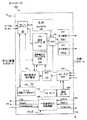
本発明に基づくトランシーバ100は、図2及び3に示される。トランシーバ100は、「光受信機サブアセンブリ(ROSA)」102及び「光送信機サブアセンブリ(TOSA)」103に加え、高速電気信号を外部に通信する関連する後置増幅器104及びレーザ駆動装置105集積回路を含む。しかし、この場合、他の全ての制御及び設定機能は、コントローラICと呼ばれる第3の単一チップ集積回路110で実行される。 A
コントローラIC110は、エンドユーザとの全ての低速通信を処理する。これらは、「信号の損失(LOS)」111、「送信機障害指示(TX FAULT)」14、及び「送信機使用不可入力(TXDIS)」13のような標準化されたピン機能を含む。コントローラIC110は、コントローラ内のメモリマップ領域にアクセスするための、メモリインタフェースとも呼ばれる2線シリアルインタフェース121を有する。以下に示される「メモリマップ表」1、2、3、及び4は、本発明の一実施形態で実施されたトランシーバコントローラの一実施形態に対する例示的なメモリマップである。尚、「メモリマップ表」1、2、3、及び4は、本明細書に説明された値及び制御機能のメモリマップを示すことに加えて、この明細書の範囲外であって、従って本発明の一部ではないいくつかのパラメータ及び制御機構も示している。 The
インタフェース121は、ホスト装置のインタフェースの入出力線、一般にはクロック(SCL)線15及びデータ(SDA)線16に連結される。好ましい実施形態では、シリアルインタフェース121は、「GBIC」及び「SFP」規格でも使用される2線シリアルインタフェース規格に従って作動するが、他のシリアルインタフェースも代替実施形態では同等に良く使用することができる。2線シリアルインタフェース121は、全ての設定とコントローラIC110の照会とのために使用され、メモリマップ装置としての光電子トランシーバの制御回路にアクセスすることを可能にする。換言すれば、表とパラメータは、コントローラ内の一又は二以上の不揮発性メモリ装置120、122、及び128(例えば、「EEPROM」装置)の所定のメモリ領域に書き込むことにより設定され、それに対して、診断用と他の出力及びステータスとの値は、同じ不揮発性メモリ装置120、122、及び128の所定のメモリ領域を読み込むことにより出力される。この手法は、「EEPROM」内に記憶された識別・能力性データを読み出すために2線シリアルインタフェースが使用される多くのトランシーバの現在規定されているシリアルID機能性と一致する。 The
尚、メモリ装置120、122、及び128内のメモリ領域のいくつかは、デュアルポートであるか、又は、更にいくつかの例ではトリプルポートである。換言すれば、これらのメモリマップ領域は、シリアルインタフェース121を通じて読み出され、ある場合には書き込むことができるが、それらはまた、コントローラ110内の別の回路により直接アクセスされる。例えば、メモリ120に記憶された特定の「マージン処理」値は、論理回路134により直接読み込まれて、D/A出力装置123に送られている駆動レベル信号を調節する(すなわち、上方又は下方にスケーリングする)ために使用される。同様に、(A)論理回路131により書き込まれた、及び、(B)論理回路131により直接読み出されたフラッグ記憶メモリ128がある。メモリ装置内にはなく実質的にデュアルポートであるメモリマップ領域の例は、クロック132の出力又は結果レジスタである。この場合、レジスタ内に累積された時間値は、シリアルインタフェース121を通じて読取り可能であるが、クロック回路132内の回路により書き込まれる。 It should be noted that some of the memory areas in the
クロック132の結果レジスタに加え、コントローラのそれぞれのサブ回路の入力又は出力におけるレジスタとして、コントローラ内の他のメモリマップ領域を利用することができる。例えば、論理回路134の作動を制御するために使用されるマージン処理値は、メモリ装置128内に記憶されずに、論理回路134又はその近くのレジスタに記憶することができる。別の例では、「ADC」127により生成された計測値をレジスタに記憶することができる。メモリインタフェース121は、対応する所定のメモリマップ領域に記憶されたデータにアクセスするように指令を受け取った時は何時でも、メモリインタフェースがこれらのレジスタのそれぞれにアクセスできるように構成される。そのような実施形態において、「メモリ内の領域」には、コントローラ全体のメモリマップレジスタが含まれる。 In addition to the
代替実施形態では、クロック132の結果レジスタ内の時間値、又はその時間値に相当する値が、メモリ128を有するメモリ領域に定期的に記憶される(例えば、これは装置作動の1分ごと、又は1時間ごとに一回実行することができる)。この代替実施形態において、インタフェース121を通じてホスト装置により読み込まれる時間値は、クロック132の結果レジスタ内の値が現在の時間値であるのとは対照的に、メモリ128に記憶された前回の時間値である。 In an alternative embodiment, the time value in the result register of
図2及び3に示されるように、コントローラIC110は、レーザ駆動装置105及び受信機構成要素と接続している。これらの接続により、多重機能が提供される。コントローラICは、多くのD/A変換器123を有している。好ましい実施形態では、D/A変換器は、電流供給装置として実装されるが、他の実施形態では、D/A変換器は電圧供給装置を使用して実行することができ、更に他の実施形態では、D/A変換器はデジタル電位差計を使用して実行することができる。好ましい実施形態では、D/A変換器の出力信号は、レーザ駆動回路105の重要なパラメータを制御するために使用される。一実施形態では、D/A変換器123の出力は、レーザバイアス電流を直接制御し、同じくレーザに対するAC変調レベル(一定バイアス作動)を制御するために使用される。別の実施形態では、コントローラ110のD/A変換器123の出力は、AC変調レベル(一定出力作動)に加えて、レーザ駆動装置105の平均出力電力レベルを制御する。 As shown in FIGS. 2 and 3, the
好ましい実施形態では、コントローラ110は、レーザの温度依存特性を補償するための機構を含む。これは、コントローラIC110内の温度センサ125により計測された温度の関数である値を制御出力に対して割り当てるために使用される温度ルックアップ表122を使用してコントローラ110内で実行される。代替実施形態では、レーザ駆動装置105の特性を制御するために、コントローラ110は、電圧供給装置出力を有するD/A変換器を使用するか、又は、一又は二以上のD/A変換器123をデジタル電位差計と置き換えることさえできる。また、図2は、レーザ駆動装置105がコントローラ110からの入力を受け入れるように特に設計されているシステムを示すが、他の多くのレーザ駆動ICを有するコントローラIC110を用いてそれらの出力特性を制御することができることにも注意すべきである。 In a preferred embodiment,
温度依存のアナログ出力制御に加えて、コントローラICは、多くの温度に依存しない(一つのメモリ設定値)アナログ出力を具備することができる。これらの温度に依存しない出力により多くの機能が提供されるが、特に関連ある一つの応用は、処理に起因するそれらの装置の特性変動を補償するためのレーザ駆動装置105又は後置増幅器104の他の設定に対するの精密調節である。この一例は、受信機の後置増幅器104の出力スイングであろう。通常は、そのようなパラメータは、設定された抵抗器を使用することで、設計時に所望の値に固定される。しかし、それは、多くの場合、後置増幅器集積回路104の製造に付随する通常の処理変動が、設定固定の抵抗器による得られる出力スイングに望ましくない変動を引き起こすことになる。本発明を使用して、追加のD/A変換器123により生成されたコントローラIC110のアナログ出力は、製造設定時における部品ごとの出力スイング設定を調節又は補償するために使用される。 In addition to temperature-dependent analog output control, the controller IC can have many temperature-independent (single memory settings) analog outputs. While these temperature-independent outputs provide more functionality, one particularly relevant application is the use of a
コントローラからレーザ駆動装置105に対する接続に加えて、図2は、レーザ駆動装置105からコントローラIC110までのいくつかの接続、及び、「ROSA」102及び後置増幅器104からコントローラIC110までの同様の接続を示す。これらは、診断フィードバックをコントローラIC内のメモリマップ領域を通じてホスト装置に提供するために、コントローラIC110が使用するアナログモニタリング接続である。好ましい実施形態のコントローラIC110は、多くのアナログ入力を有する。アナログ入力信号は、トランシーバ及び/又は受信機回路の作動条件を指示する。これらのアナログ信号は、マルチプレクサ124により走査され、アナログ/デジタル変換器(ADC)127を使用して変換される。ADC127は、好ましい実施形態では12ビットの分解能を有するが、別の実施形態では、別の分解能レベルのADCを使用することができる。変換値は、所定のメモリ領域、例えば図3に示される診断値及びフラッグ記憶装置128に記憶され、メモリの読み込みを通じてホスト装置に対してアクセス可能である。これらの値は、工場での較正手順の一部として、標準単位(ミリボルト又はマイクロワットのような)に対して較正される。 In addition to the connection from the controller to the
コントローラIC内のメモリマップ領域に記憶されたデジタル化された量は、以下に限定されるものではないが、レーザバイアス電流、送信レーザ出力、及び、受信出力(「ROSA」102内のフォトダイオード検知器により計測される)を含む。メモリマップ表(例えば、表1)において、計測レーザバイアス電流は、パラメータBinとして示され、計測送信レーザ出力は、Pinとして示され、計測受信出力はRinとして示される。メモリマップ表は、典型的な実施形態においてこれらの計測値が記憶されているメモリ領域を示し、また、対応する限界値、フラッグ値、及び設定値(例えば、フラッグの極性を指示するための)がどこに記憶されているかを示す。The digitized quantities stored in the memory map area in the controller IC are not limited to the following: laser bias current, transmit laser output, and receive output (photodiode detection in “ROSA” 102) Measured by the instrument). Memory Map Table (e.g., Table 1), the measured laser bias current is denoted as parameter Bin, the measured transmitted laser power is denoted as Pin, measured received power is denoted as Rin. The memory map table shows the memory areas where these measurements are stored in the exemplary embodiment, and the corresponding limit values, flag values, and set values (eg, to indicate the polarity of the flags). Indicates where is stored.
図3に示されるように、コントローラ110は、電圧供給センサ126を含む。このセンサにより生成されたアナログ電圧レベル信号は、ADC127によりデジタル電圧レベル信号に変換され、このデジタル電圧レベル信号は、メモリ128に記憶される。好ましい実施形態では、A/D入力「mux」124及びADC127は、モニタされた信号をデジタル信号に自動的に定期的に変換してこれらのデジタル値をメモリ128内に記憶するように、クロック信号により制御される。 As shown in FIG. 3, the
更に、デジタル値が生成されると、コントローラの値比較論理回路131は、これらの値を所定の限界値と比較する。限界値は、工場でメモリ128内に好ましくは記憶されるが、ホスト装置が最初にプログラムされていた限界値を新しい限界値で上書きしてもよい。モニタされた各信号は、下限値及び上限値と自動的に比較され、診断値及びフラッグ記憶装置128にその後記憶される二つの限界フラッグ値が生成されることになる。意味のある上限値又は下限値のない任意のモニタ信号に対しては、限界値をフラッグが決して立たないような値に設定することができる。 In addition, once the digital values are generated, the controller's
限界フラッグはまた、時に警報及び警告呼び出しフラッグでもある。ホスト装置(又は、エンドユーザ)は、トランシーバリンクに障害を引き起こした可能性が高い条件(警報フラッグ)が存在するかどうか、又は、障害がすぐに発生する可能性が高いと予想する条件が存在するかどうかを判断するために、これらのフラッグをモニタすることができる。そのような条件の例は、ゼロまで下降して送信機出力の即座の障害を指示するレーザバイアス電流であり、又は、定格値を50%を超えて上回り、レーザの寿命終了の条件を指示する一定出力モードのレーザバイアス電流であろう。従って、自動的に生成された限界フラッグは、内部に記憶された限界値に基づいてトランシーバの機能性に対して単純な合否の決定を下すので有益である。 The limit flag is also sometimes an alarm and warning call flag. The host device (or end user) has a condition (alarm flag) that is likely to cause a failure in the transceiver link, or a condition that the failure is likely to occur soon These flags can be monitored to determine whether to do so. An example of such a condition is a laser bias current that drops to zero and indicates an immediate failure of the transmitter output, or exceeds the rated value by more than 50%, indicating a condition for the end of life of the laser. It will be the laser bias current in constant output mode. Thus, the automatically generated limit flag is beneficial because it makes a simple pass / fail decision to the functionality of the transceiver based on the limit values stored therein.
好ましい実施形態では、障害制御及び論理回路133は、内部「LOS(信号の損失)」入力及び「障害入力」信号と共に、警報及び警告フラッグの論理和を取り、ホストインタフェースに連結されて、従ってホスト装置に利用可能にされた2進トランシーバ障害(TxFault)信号を生成する。ホスト装置は、「TxFault」信号をモニタし、警報又は警告の原因を判断するために、トランシーバ内の全ての警報及び警告フラッグと、同じく対応するモニタ信号を自動的に読み出すことにより、「TxFault」信号の表明に応答するようにプログラムすることができる。
障害制御及び論理回路133は、更に、受信回路(図2の「ROSA」)から受け取った信号損失(LOS)信号をホストインタフェースに伝達する。In the preferred embodiment, the fault control and
The fault control and
障害制御及び論理回路133の別の機能は、目の安全を保証する必要がある時に、送信機(図2の「TOSA」)の作動を使用不可にすることである。レーザ駆動装置の状態と「Tx Disable」出力との間には、規格で規定された対話があり、それは、障害制御及び論理回路133により実行される。論理回路133が目の安全に対して危険になり得る問題を検知すると、コントローラの「Tx Diable」信号の作動によりレーザ駆動装置が使用不可にされる。ホスト装置は、ホストインタフェースの「TxDisableCmd」線上で指令信号を送ることにより、この条件をリセットすることができる。
障害制御及び論理回路133の更に別の機能は、メモリ128に記憶された一組の設定フラッグの決定に従って、その入力信号及び出力信号の極性を判断することである。例えば、回路133の「信号の損失(LOS)」出力は、メモリ128に記憶された対応する設定フラッグにより判断される時、論理「ロー」にも論理「ハイ」にもすることができる。Another function of the fault control and
Yet another function of the fault control and
メモリ128に記憶された他の設定フラッグ(表4参照)は、警告及び警報フラッグの各々の極性を判断するために使用される。メモリ128に記憶された更に別の設定値は、それぞれのモニタされたアナログ信号をデジタル信号に変換する時に「ADC」127により適用されたスケーリングを判断するために使用される。
代替実施形態では、ホストインタフェースにおけるコントローラ110に対する別の入力は、速度選択信号である。図3において、速度選択信号は、論理回路133に入力される。このホスト生成信号は、通常は、受信機(ROSA102)により受け取られるデータの期待されるデータ速度を特定するデジタル信号であろう。例えば、速度選択信号は、高速及び低速(例えば、2.5Gb/s及び1.25Gb/s)のデータ速度を表す二つの値を有する。コントローラは、速度選択信号により特定された値に対応する帯域幅にアナログ受信回路を設定するための制御信号を生成することにより、速度選択信号に応答する。Other setting flags (see Table 4) stored in
In an alternative embodiment, another input to the
上述の機能の全ての組合せがこのトランシーバコントローラの好ましい実施形態には望ましいが、同業者には、これらの機能のサブセットのみを実施する装置もまた大いに役立つことが明白である。同様に、本発明は、送信機及び受信機に適用可能であり、ただ単にトランシーバだけに適用されるわけではない。最後に、本発明のコントローラが、マルチチャンネルの光リンクの用途に適切であることに注目すべきである。
Although all combinations of the above functions are desirable for the preferred embodiment of this transceiver controller, it will be apparent to those skilled in the art that an apparatus that implements only a subset of these functions is also of great help. Similarly, the present invention is applicable to transmitters and receivers, not just transceivers. Finally, it should be noted that the controller of the present invention is suitable for multi-channel optical link applications.

110 コントローラ
120、122、128 メモリ
121 シリアルインタフェース
123−1、123−2 制御回路
127 アナログ/デジタル変換回路
131 比較論理回路110
Claims (19)
Translated fromJapaneseトランシーバに関連する情報を記憶するための一又は二以上のメモリアレーを含むメモリと、
レーザ送信機及びフォトダイオード受信機から複数のアナログ信号を受信し、該受信アナログ信号をデジタル値に変換し、該デジタル値を前記メモリ内の所定の領域に記憶するためのアナログ/デジタル変換回路と、
前記メモリに記憶された一又は二以上の値に従って、前記レーザ送信機の作動を制御する制御信号を発生するように構成された制御回路と、
前記メモリ内の領域に対して読取り及び書込みを行うためのインタフェースと、
前記デジタル値を限界値と比較し、該限界値に基づいてフラッグ値を発生させ、該フラッグ値を前記メモリ内の所定の領域に記憶するための比較論理回路と、
を含むことを特徴とする回路。A single chip integrated circuit for controlling an optoelectronic transceiver having a laser transmitter and a photodiode receiver,
A memory including one or more memory arrays for storing information associated with the transceiver;
An analog / digital conversion circuit for receiving a plurality of analog signals from a laser transmitter and a photodiode receiver, converting the received analog signals into digital values, and storing the digital values in a predetermined area in the memory; ,
A control circuit configured to generate a control signal for controlling operation of the laser transmitter according to one or more values stored in the memory;
An interface for reading and writing to an area in the memory;
A comparison logic circuit for comparing the digital value with a limit value, generating a flag value based on the limit value, and storing the flag value in a predetermined area in the memory;
A circuit comprising:
前記発生された時間値は、前記インタフェースを通じて読込可能である、
ことを特徴とする請求項1に記載の単一チップ集積回路。A cumulative clock for generating a time value corresponding to the cumulative operating time of the transceiver;
The generated time value is readable through the interface;
The single-chip integrated circuit according to claim 1.
を更に含み、
前記アナログ/デジタル変換回路は、該電力レベル信号をデジタル電力レベル値に変換し、該デジタル電力レベル値を前記メモリ内の所定の電力レベル領域に記憶するように構成される、
ことを特徴とする請求項1に記載の単一チップ集積回路。A power supply voltage sensor coupled to the analog / digital conversion circuit for generating a power level signal corresponding to a power supply voltage level of the transceiver;
Further including
The analog / digital conversion circuit is configured to convert the power level signal into a digital power level value and store the digital power level value in a predetermined power level region in the memory.
The single-chip integrated circuit according to claim 1.
を更に含み、
前記アナログ/デジタル変換回路は、該温度信号をデジタル温度値に変換し、該デジタル温度値を前記メモリ内の所定の温度領域に記憶するように構成される、
ことを特徴とする請求項1に記載の単一チップ集積回路。A temperature sensor coupled to the analog / digital conversion circuit for generating a temperature signal corresponding to the temperature of the transceiver;
Further including
The analog / digital conversion circuit is configured to convert the temperature signal into a digital temperature value and store the digital temperature value in a predetermined temperature region in the memory.
The single-chip integrated circuit according to claim 1.
を更に含み、
前記障害処理論理回路が、前記トランシーバから受信した前記少なくとも一つの障害信号と、前記メモリから受信した前記少なくとも一つのフラッグ値とを論理的に結合して前記計算された障害信号を発生させるための計算論理回路を含む、
ことを特徴とする請求項1に記載の単一チップ集積回路。To receive at least one fault signal from the transceiver and to be coupled to the transceiver to receive at least one flag value stored in the memory and to transmit a calculated fault signal Fault handling logic coupled to the host interface,
Further including
The fault processing logic for logically combining the at least one fault signal received from the transceiver and the at least one flag value received from the memory to generate the calculated fault signal; Including computational logic,
The single-chip integrated circuit according to claim 1.
該光電子装置から該光電子装置の作動条件に対応する複数のアナログ信号を受信し、該受信アナログ信号をデジタル値に変換し、該デジタル値を前記メモリ内の所定の領域に記憶するためのアナログ/デジタル変換回路と、
ホスト装置から受信した指令に従って前記メモリ内の領域に対して読取り及び書込みを行うためのメモリインタフェースと、
を含むことを特徴とする、光電子装置を制御するための単一チップ集積回路。A memory including one or more memory arrays for storing information related to the optoelectronic device;
Receiving a plurality of analog signals corresponding to operating conditions of the optoelectronic device from the optoelectronic device, converting the received analog signal into a digital value, and storing the digital value in a predetermined area in the memory; A digital conversion circuit;
A memory interface for reading and writing to an area in the memory according to a command received from a host device;
A single chip integrated circuit for controlling an optoelectronic device.
レーザ送信機及びフォトダイオード受信機から複数のアナログ信号を受信し、該受信アナログ信号をデジタル値に変換し、該デジタル値を集積回路内の所定のメモリマップ領域に記憶するためのアナログ/デジタル変換回路と、
前記デジタル値を限界値と比較し、該限界値に基づいてフラッグ値を発生し、該フラッグ値を集積回路内の所定のメモリマップ領域に記憶するための比較論理回路と、
集積回路内に記憶された一又は二以上の値に従って、前記レーザ送信機の作動を制御する制御信号を発生するように構成された制御回路と、
集積回路内の領域に対して読取り及び書込みを行い、該制御回路の作動を制御するために集積回路内のメモリマップ領域にアクセスするためのメモリマップインタフェースと、 を含むことを特徴とする回路。A single chip integrated circuit for controlling an optoelectronic transceiver having a laser transmitter and a photodiode receiver,
Analog / digital conversion for receiving a plurality of analog signals from a laser transmitter and a photodiode receiver, converting the received analog signals into digital values, and storing the digital values in a predetermined memory map area in the integrated circuit Circuit,
A comparison logic circuit for comparing the digital value with a limit value, generating a flag value based on the limit value, and storing the flag value in a predetermined memory map area in the integrated circuit;
A control circuit configured to generate a control signal for controlling operation of the laser transmitter according to one or more values stored in an integrated circuit;
A memory map interface for reading from and writing to areas in the integrated circuit and accessing a memory map area in the integrated circuit to control operation of the control circuit.
ホスト装置から受信した命令に従って、メモリ内の領域に対して読取り及び書込みを行う段階と、
レーザ送信機及びフォトダイオード受信機から複数のアナログ信号を受信し、該受信アナログ信号をデジタル値に変換し、該デジタル値を前記メモリ内の所定の領域に記憶する段階と、
該デジタル値を限界値と比較し、該限界値に基づいてフラッグ値を発生し、該フラッグ値を前記メモリ内の所定の領域に記憶する段階と、
前記メモリ内に記憶された一又は二以上の値に従って前記レーザ送信機の作動を制御する制御信号を発生させる段階と、
を含むことを特徴とする方法。A method for controlling an optoelectronic transceiver having a laser transmitter and a photodiode receiver, the method comprising:
Reading and writing to areas in the memory according to instructions received from the host device;
Receiving a plurality of analog signals from a laser transmitter and a photodiode receiver, converting the received analog signals into digital values, and storing the digital values in a predetermined area in the memory;
Comparing the digital value with a limit value, generating a flag value based on the limit value, and storing the flag value in a predetermined area in the memory;
Generating a control signal for controlling operation of the laser transmitter in accordance with one or more values stored in the memory;
A method comprising the steps of:
を更に含み、
前記発生した時間値は、前記メモリインタフェースを通じて前記ホスト装置により読込可能である、
ことを特徴とする請求項10に記載の方法。Generating a time value corresponding to a cumulative operating time of the transceiver;
Further including
The generated time value is readable by the host device through the memory interface.
The method according to claim 10.
光電子装置から該光電子装置の作動条件に対応する複数のアナログ信号を受信し、該受信アナログ信号をデジタル値に変換し、該デジタル値を前記メモリ内の所定の領域に記憶する段階と、
を含み、
単一チップコントローラ集積回路により実行される、
ことを特徴とする、光電子装置を制御する方法。Reading and writing to areas in the memory according to instructions received from the host device;
Receiving a plurality of analog signals corresponding to operating conditions of the optoelectronic device from the optoelectronic device, converting the received analog signal into a digital value, and storing the digital value in a predetermined area in the memory;
Including
Performed by a single chip controller integrated circuit,
A method of controlling an optoelectronic device.
ホスト装置から受信した命令に従って、光電子トランシーバのコントローラ内のメモリマップ領域に対して読取り及び書込みを行う段階と、
レーザ送信機及びフォトダイオード受信機から複数のアナログ信号を受信し、該受信アナログ信号をデジタル値に変換し、該デジタル値を前記コントローラ内の所定のメモリマップ領域に記憶する段階と、
該デジタル値を限界値と比較し、該限界値に基づいてフラッグ値を発生し、該フラッグ値を前記コントローラ内の所定のメモリマップ領域に記憶する段階と、
該コントローラ内の該所定のメモリマップ領域に記憶された一又は二以上の値に従って、前記レーザ送信機の作動を制御する制御信号を発生させる段階と、
を含み,
前記レーザ送信機及びフォトダイオード受信機から複数のアナログ信号を受信するアナログ/デジタル変換回路は、該受信アナログ信号をデジタル値に変換し、該デジタル値を前記コントローラ内の所定のメモリマップ領域に記憶する、
ことを特徴とする方法。A method for controlling an optoelectronic transceiver having a laser transmitter and a photodiode receiver, the method comprising:
Reading and writing to a memory-mapped area in the controller of the optoelectronic transceiver according to instructions received from the host device;
Receiving a plurality of analog signals from a laser transmitter and a photodiode receiver, converting the received analog signals into digital values, and storing the digital values in a predetermined memory map area in the controller;
Comparing the digital value with a limit value, generating a flag value based on the limit value, and storing the flag value in a predetermined memory map area in the controller;
Generating a control signal for controlling the operation of the laser transmitter according to one or more values stored in the predetermined memory map area in the controller;
Including
An analog / digital conversion circuit that receives a plurality of analog signals from the laser transmitter and the photodiode receiver converts the received analog signals into digital values and stores the digital values in a predetermined memory map area in the controller. To
A method characterized by that.
を更に含み、
該時間値が存在する該レジスタは、前記読取り段階により前記コントローラ内のメモリマップとしてアクセスされる、
ことを特徴とする請求項18に記載の方法。Generating and storing in a register a time value corresponding to the cumulative operating time of the transceiver;
Further including
The register in which the time value is present is accessed as a memory map in the controller by the read stage.
The method according to claim 18, wherein:
Applications Claiming Priority (1)
| Application Number | Priority Date | Filing Date | Title |
|---|---|---|---|
| US09/777,917US7079775B2 (en) | 2001-02-05 | 2001-02-05 | Integrated memory mapped controller circuit for fiber optics transceiver |
Related Parent Applications (1)
| Application Number | Title | Priority Date | Filing Date |
|---|---|---|---|
| JP2002563630ADivisionJP3822861B2 (en) | 2001-02-05 | 2002-02-04 | Integrated Memory Map Controller Circuit for Fiber Optic Transceivers |
Related Child Applications (1)
| Application Number | Title | Priority Date | Filing Date |
|---|---|---|---|
| JP2006082561ADivisionJP4557916B2 (en) | 2001-02-05 | 2006-03-24 | Integrated Memory Map Controller Circuit for Fiber Optic Transceivers |
Publications (2)
| Publication Number | Publication Date |
|---|---|
| JP2006136029Atrue JP2006136029A (en) | 2006-05-25 |
| JP4414968B2 JP4414968B2 (en) | 2010-02-17 |
Family
ID=25111692
Family Applications (3)
| Application Number | Title | Priority Date | Filing Date |
|---|---|---|---|
| JP2002563630AExpired - LifetimeJP3822861B2 (en) | 2001-02-05 | 2002-02-04 | Integrated Memory Map Controller Circuit for Fiber Optic Transceivers |
| JP2006015985AExpired - LifetimeJP4414968B2 (en) | 2001-02-05 | 2006-01-25 | Integrated Memory Map Controller Circuit for Fiber Optic Transceivers |
| JP2006082561AExpired - LifetimeJP4557916B2 (en) | 2001-02-05 | 2006-03-24 | Integrated Memory Map Controller Circuit for Fiber Optic Transceivers |
Family Applications Before (1)
| Application Number | Title | Priority Date | Filing Date |
|---|---|---|---|
| JP2002563630AExpired - LifetimeJP3822861B2 (en) | 2001-02-05 | 2002-02-04 | Integrated Memory Map Controller Circuit for Fiber Optic Transceivers |
Family Applications After (1)
| Application Number | Title | Priority Date | Filing Date |
|---|---|---|---|
| JP2006082561AExpired - LifetimeJP4557916B2 (en) | 2001-02-05 | 2006-03-24 | Integrated Memory Map Controller Circuit for Fiber Optic Transceivers |
Country Status (13)
| Country | Link |
|---|---|
| US (16) | US7079775B2 (en) |
| EP (3) | EP1471671B1 (en) |
| JP (3) | JP3822861B2 (en) |
| KR (1) | KR100684461B1 (en) |
| CN (2) | CN1294709C (en) |
| AT (3) | ATE429051T1 (en) |
| AU (1) | AU2002238034B2 (en) |
| CA (2) | CA2687686C (en) |
| CZ (1) | CZ300439B6 (en) |
| DE (3) | DE60219140T2 (en) |
| ES (2) | ES2281506T3 (en) |
| IL (1) | IL157192A (en) |
| WO (1) | WO2002063800A1 (en) |
Cited By (2)
| Publication number | Priority date | Publication date | Assignee | Title |
|---|---|---|---|---|
| JP2008005061A (en)* | 2006-06-20 | 2008-01-10 | Allied Telesis Holdings Kk | Automatic adaptive SFP port |
| US7912375B2 (en) | 2008-12-15 | 2011-03-22 | Mitsubishi Electric Corporation | Optical transceiver |
Families Citing this family (313)
| Publication number | Priority date | Publication date | Assignee | Title |
|---|---|---|---|---|
| US8188878B2 (en) | 2000-11-15 | 2012-05-29 | Federal Law Enforcement Development Services, Inc. | LED light communication system |
| US6608727B2 (en)* | 2001-01-29 | 2003-08-19 | Hitachi Global Storage Technologies Netherlands, B.V. | Method and apparatus for determining the tribology for a head/disk interface |
| US7302186B2 (en)* | 2001-02-05 | 2007-11-27 | Finisar Corporation | Optical transceiver and host adapter with memory mapped monitoring circuitry |
| US7079775B2 (en) | 2001-02-05 | 2006-07-18 | Finisar Corporation | Integrated memory mapped controller circuit for fiber optics transceiver |
| US20040197101A1 (en)* | 2001-02-05 | 2004-10-07 | Sasser Gary D. | Optical transceiver module with host accessible on-board diagnostics |
| US7149430B2 (en) | 2001-02-05 | 2006-12-12 | Finsiar Corporation | Optoelectronic transceiver having dual access to onboard diagnostics |
| US7346278B2 (en)* | 2001-02-05 | 2008-03-18 | Finisar Corporation | Analog to digital signal conditioning in optoelectronic transceivers |
| US6668240B2 (en) | 2001-05-03 | 2003-12-23 | Emerson Retail Services Inc. | Food quality and safety model for refrigerated food |
| US6892546B2 (en) | 2001-05-03 | 2005-05-17 | Emerson Retail Services, Inc. | System for remote refrigeration monitoring and diagnostics |
| US7062164B2 (en)* | 2001-06-27 | 2006-06-13 | International Business Machines Corporation | Detection of data transmission rates using passing frequency-selective filtering |
| US7174106B2 (en)* | 2001-08-13 | 2007-02-06 | Finisar Corporation | Multi-rate and multi-level gigabit interface converter |
| US6853259B2 (en)* | 2001-08-15 | 2005-02-08 | Gallitzin Allegheny Llc | Ring oscillator dynamic adjustments for auto calibration |
| US6975642B2 (en) | 2001-09-17 | 2005-12-13 | Finisar Corporation | Optoelectronic device capable of participating in in-band traffic |
| DE60133207T2 (en)* | 2001-12-13 | 2009-04-30 | Alcatel Lucent | Laser transmitter and method for transmitting controlled optical signals |
| EP1485736B1 (en)* | 2002-02-12 | 2007-06-13 | Finisar Corporation | Maintaining desirable performance of optical emitters at extreme temperatures |
| EP1788413A3 (en)* | 2002-02-12 | 2007-06-13 | Finisar Corporation | Maintaining desirable performance of optical emitters at extreme temperatures |
| US6947455B2 (en) | 2002-02-12 | 2005-09-20 | Finisar Corporation | Maintaining desirable performance of optical emitters at extreme temperatures |
| US6862302B2 (en)* | 2002-02-12 | 2005-03-01 | Finisar Corporation | Maintaining desirable performance of optical emitters over temperature variations |
| JP4430280B2 (en)* | 2002-04-18 | 2010-03-10 | 日本オプネクスト株式会社 | Optical transmission equipment |
| JP3945308B2 (en)* | 2002-05-09 | 2007-07-18 | 住友電気工業株式会社 | Optical transmitter |
| US7486894B2 (en)* | 2002-06-25 | 2009-02-03 | Finisar Corporation | Transceiver module and integrated circuit with dual eye openers |
| US7561855B2 (en) | 2002-06-25 | 2009-07-14 | Finisar Corporation | Transceiver module and integrated circuit with clock and data recovery clock diplexing |
| US7664401B2 (en) | 2002-06-25 | 2010-02-16 | Finisar Corporation | Apparatus, system and methods for modifying operating characteristics of optoelectronic devices |
| US7437079B1 (en) | 2002-06-25 | 2008-10-14 | Finisar Corporation | Automatic selection of data rate for optoelectronic devices |
| US7809275B2 (en) | 2002-06-25 | 2010-10-05 | Finisar Corporation | XFP transceiver with 8.5G CDR bypass |
| US7269357B2 (en)* | 2002-08-02 | 2007-09-11 | Finisar Corporation | Transceiver with programmable signal parameters |
| US7177547B1 (en)* | 2002-08-02 | 2007-02-13 | Finisar Corporation | System and method for controlling polarity of a data signal |
| US7477847B2 (en) | 2002-09-13 | 2009-01-13 | Finisar Corporation | Optical and electrical channel feedback in optical transceiver module |
| WO2004038473A1 (en)* | 2002-10-22 | 2004-05-06 | Firecomms Limited | Connection of optical waveguides to optical devices |
| JP4094931B2 (en)* | 2002-10-29 | 2008-06-04 | 三菱電機株式会社 | Transceiver integrated circuit and communication module |
| US6889173B2 (en) | 2002-10-31 | 2005-05-03 | Emerson Retail Services Inc. | System for monitoring optimal equipment operating parameters |
| US7356262B2 (en)* | 2002-11-06 | 2008-04-08 | Finisar Corporation | Time division multiplexing of analog signals in an optical transceiver |
| CA2504622A1 (en)* | 2002-11-06 | 2004-06-17 | Finisar Corporation | Control of peaking of laser driver current to improve eye quality |
| US7230961B2 (en) | 2002-11-08 | 2007-06-12 | Finisar Corporation | Temperature and jitter compensation controller circuit and method for fiber optics device |
| US7317743B2 (en)* | 2002-11-08 | 2008-01-08 | Finisar Corporation | Temperature and jitter compensation controller circuit and method for fiber optics device |
| AU2003295703A1 (en)* | 2002-11-20 | 2004-06-15 | Bookham Technology, Plc | Optical transceiver module with improved ddic and methods of use |
| US20040102874A1 (en)* | 2002-11-27 | 2004-05-27 | Crosby Philip S. | Method and apparatus for controlling an optical transponder |
| US7539423B2 (en)* | 2003-01-10 | 2009-05-26 | Avago Technologies Fiber Ip (Singapore) Pte. Ltd. | Loss of signal detection and programmable behavior after error detection |
| US20040136708A1 (en)* | 2003-01-15 | 2004-07-15 | Woolf Kevin Reid | Transceiver configured to store failure analysis information |
| US20040136720A1 (en)* | 2003-01-15 | 2004-07-15 | Mahowald Peter H. | Task prioritization in firmware controlled optical transceiver |
| US7668512B2 (en)* | 2003-01-15 | 2010-02-23 | Avago Technologies Fiber Ip (Singapore) Pte. Ltd. | Transceiver with a test mode of operation |
| US6961259B2 (en)* | 2003-01-23 | 2005-11-01 | Micron Technology, Inc. | Apparatus and methods for optically-coupled memory systems |
| US7002131B1 (en) | 2003-01-24 | 2006-02-21 | Jds Uniphase Corporation | Methods, systems and apparatus for measuring average received optical power |
| US7215883B1 (en) | 2003-01-24 | 2007-05-08 | Jds Uniphase Corporation | Methods for determining the performance, status, and advanced failure of optical communication channels |
| US7528643B2 (en)* | 2003-02-12 | 2009-05-05 | Semiconductor Energy Laboratory Co., Ltd. | Semiconductor device, electronic device having the same, and driving method of the same |
| DE10305986B4 (en)* | 2003-02-12 | 2022-07-21 | IAD Gesellschaft für Informatik, Automatisierung und Datenverarbeitung mbH | Measuring system with intelligent sensor head for medium or high voltage systems or in mining |
| US7463674B2 (en)* | 2003-04-09 | 2008-12-09 | Avago Technologies Fiber Ip (Singapore) Pte. Ltd. | Tables for determining the signal strength of a received signal in a fibre optics transceiver |
| US7215891B1 (en) | 2003-06-06 | 2007-05-08 | Jds Uniphase Corporation | Integrated driving, receiving, controlling, and monitoring for optical transceivers |
| US9337948B2 (en)* | 2003-06-10 | 2016-05-10 | Alexander I. Soto | System and method for performing high-speed communications over fiber optical networks |
| US8068739B2 (en)* | 2003-06-12 | 2011-11-29 | Finisar Corporation | Modular optical device that interfaces with an external controller |
| GB2405264B (en)* | 2003-08-20 | 2007-02-28 | Agilent Technologies Inc | Pluggable optical subassembly |
| US20050060114A1 (en)* | 2003-08-29 | 2005-03-17 | Finisar | Testing and storing tuning information in modular optical devices |
| US9065571B2 (en)* | 2003-08-29 | 2015-06-23 | Finisar Corporation | Modular controller that interfaces with modular optical device |
| US8923704B2 (en)* | 2003-08-29 | 2014-12-30 | Finisar Corporation | Computer system with modular optical devices |
| US8891970B2 (en)* | 2003-08-29 | 2014-11-18 | Finisar Corporation | Modular optical device with mixed signal interface |
| GB2406237B (en)* | 2003-09-20 | 2007-08-08 | Agilent Technologies Inc | An electro-optical communication system |
| US7233740B2 (en)* | 2003-09-29 | 2007-06-19 | Avago Technologies Fiber Ip (Singapore) Pte. Ltd. | Self-characterizing and self-programming optical transmitter |
| JP4599822B2 (en)* | 2003-10-08 | 2010-12-15 | 住友電気工業株式会社 | Optical transceiver |
| US7440647B2 (en)* | 2003-10-09 | 2008-10-21 | Finisar Corporation | Integrated optical assembly |
| US8750725B2 (en)* | 2003-11-18 | 2014-06-10 | Finisar Corporation | Digital optical receiving module, and a method for monitoring the signal quality of a transmitted, modulated optical signal |
| US8165297B2 (en) | 2003-11-21 | 2012-04-24 | Finisar Corporation | Transceiver with controller for authentication |
| DE10357416A1 (en)* | 2003-12-03 | 2005-07-14 | Siemens Ag | Arrangement for connecting an optical waveguide with a microprocessor-controlled electrical device |
| US7347632B2 (en)* | 2003-12-12 | 2008-03-25 | Mina Farr | Optical connectors for electronic devices |
| US8667194B2 (en)* | 2003-12-15 | 2014-03-04 | Finisar Corporation | Two-wire interface in which a master component monitors the data line during the preamble generation phase for synchronization with one or more slave components |
| US7426586B2 (en)* | 2003-12-15 | 2008-09-16 | Finisar Corporation | Configurable input/output terminals |
| US7702030B2 (en)* | 2003-12-17 | 2010-04-20 | Mindspeed Technologies, Inc. | Module to module signaling with jitter modulation |
| US20050135756A1 (en) | 2003-12-19 | 2005-06-23 | Chao Zhang | Bi-directional optical transceiver module having automatic-restoring unlocking mechanism |
| US7570672B2 (en)* | 2004-02-02 | 2009-08-04 | Simplexgrinnell Lp | Fiber optic multiplex modem |
| US7356681B2 (en)* | 2004-03-05 | 2008-04-08 | Finisar Corporation | Transient transceiver clock configuration |
| US8225024B2 (en)* | 2004-03-05 | 2012-07-17 | Finisar Corporation | Use of a first two-wire interface communication to support the construction of a second two-wire interface communication |
| US7765348B2 (en)* | 2004-03-05 | 2010-07-27 | Finisar Corporation | Configurable two-wire interface module |
| WO2005088462A1 (en)* | 2004-03-05 | 2005-09-22 | Finisar Corporation | Hierarchical and byte-configurable memory in an optical transceiver |
| US7630631B2 (en)* | 2004-04-14 | 2009-12-08 | Finisar Corporation | Out-of-band data communication between network transceivers |
| US7412842B2 (en) | 2004-04-27 | 2008-08-19 | Emerson Climate Technologies, Inc. | Compressor diagnostic and protection system |
| TWI244278B (en) | 2004-06-04 | 2005-11-21 | Ind Tech Res Inst | Optical transceiver module |
| US7493048B2 (en)* | 2004-06-30 | 2009-02-17 | Finisar Corporation | Transceiver with persistent logging mechanism |
| US8639122B2 (en)* | 2004-07-02 | 2014-01-28 | Finisar Corporation | Filtering digital diagnostics information in an optical transceiver prior to reporting to host |
| US7447438B2 (en)* | 2004-07-02 | 2008-11-04 | Finisar Corporation | Calibration of digital diagnostics information in an optical transceiver prior to reporting to host |
| US20060013540A1 (en)* | 2004-07-19 | 2006-01-19 | Chao Zhang | Single fiber optical transceiver module |
| US7583902B2 (en)* | 2004-08-10 | 2009-09-01 | Mindspeed Technologies, Inc. | Module to module signaling utilizing amplitude modulation |
| US7275377B2 (en) | 2004-08-11 | 2007-10-02 | Lawrence Kates | Method and apparatus for monitoring refrigerant-cycle systems |
| US7504610B2 (en)* | 2004-09-03 | 2009-03-17 | Mindspeed Technologies, Inc. | Optical modulation amplitude compensation system having a laser driver with modulation control signals |
| US8705973B2 (en)* | 2004-09-07 | 2014-04-22 | Finisar Corporation | Optical transceiver with off-transceiver logging mechanism |
| TWI330474B (en)* | 2004-09-21 | 2010-09-11 | Emcore Corp | Method and apparatus for distortion control for optical transmitters |
| US7548675B2 (en)* | 2004-09-29 | 2009-06-16 | Finisar Corporation | Optical cables for consumer electronics |
| US7706692B2 (en)* | 2004-09-29 | 2010-04-27 | Finisar Corporation | Consumer electronics with optical communication interface |
| US7787767B2 (en)* | 2007-04-05 | 2010-08-31 | Emcore Corporation | Eye safety in electro-optical transceivers |
| US7532820B2 (en) | 2004-10-29 | 2009-05-12 | Finisar Corporation | Systems and methods for providing diagnostic information using EDC transceivers |
| US20060099566A1 (en)* | 2004-11-08 | 2006-05-11 | Priem Rhonda K | Designer's choice chalkboard |
| US7276682B2 (en)* | 2004-11-19 | 2007-10-02 | Mindspeed Technologies, Inc. | Laser power control with automatic compensation |
| US20060110157A1 (en)* | 2004-11-22 | 2006-05-25 | Infineon Technologies North America Corp. | Transceiver with interrupt unit |
| US7350986B2 (en)* | 2004-12-30 | 2008-04-01 | Finisar Corporation | Microcode-driven programmable receive power levels in an optical transceiver |
| US7295750B2 (en)* | 2004-12-30 | 2007-11-13 | Finisar Corporation | Access key enabled update of an optical transceiver |
| US7751717B2 (en)* | 2004-12-30 | 2010-07-06 | Finisar Corporation | Host printed circuit board with multiple optical transceivers |
| US7970283B2 (en)* | 2005-03-07 | 2011-06-28 | Finisar Corporation | High speed SFP transceiver |
| JP2006319893A (en)* | 2005-05-16 | 2006-11-24 | Sumitomo Electric Ind Ltd | Optical module |
| JP2006324801A (en)* | 2005-05-17 | 2006-11-30 | Sumitomo Electric Ind Ltd | Optical transmission module |
| JP2006325030A (en)* | 2005-05-19 | 2006-11-30 | Sumitomo Electric Ind Ltd | Optical data link and optical data link control method |
| US8036539B2 (en)* | 2005-06-28 | 2011-10-11 | Finisar Corporation | Gigabit ethernet longwave optical transceiver module having amplified bias current |
| US7331819B2 (en)* | 2005-07-11 | 2008-02-19 | Finisar Corporation | Media converter |
| US7729618B2 (en) | 2005-08-30 | 2010-06-01 | Finisar Corporation | Optical networks for consumer electronics |
| US7516897B1 (en) | 2005-09-07 | 2009-04-14 | Kinana Hussain | Digital automatic power control loop for continuous and burst mode applications |
| US7860398B2 (en) | 2005-09-15 | 2010-12-28 | Finisar Corporation | Laser drivers for closed path optical cables |
| US7653314B2 (en)* | 2005-09-16 | 2010-01-26 | Finisar Corporation | Optical transceiver with custom logging mechanism |
| JP4624898B2 (en)* | 2005-09-28 | 2011-02-02 | 富士通株式会社 | Optical transmission equipment |
| US20070092257A1 (en)* | 2005-10-21 | 2007-04-26 | Smith Dale T | Optical interface for communicating optical transceiver status information |
| US8532499B2 (en)* | 2005-10-25 | 2013-09-10 | Emcore Corporation | Optical transmitter with adaptively controlled optically linearized modulator |
| US20070092262A1 (en)* | 2005-10-25 | 2007-04-26 | Donald Bozarth | Adaptive optical transmitter for use with externally modulated lasers |
| US7787766B2 (en)* | 2005-12-06 | 2010-08-31 | Jds Uniphase Corporation | Fault sensor for a laser driver circuit |
| US7853155B2 (en)* | 2005-12-12 | 2010-12-14 | Emcore Corporation | Method for adjusting bias in optical transmitter with external modulator |
| US7463802B2 (en)* | 2006-01-13 | 2008-12-09 | Emcore Corporation | Integrated circuit for adjusting bias in optical transmitter with external modulator |
| US7853154B2 (en)* | 2006-01-13 | 2010-12-14 | Mindspeed Technologies, Inc. | Bias circuit for burst-mode/TDM systems with power save feature |
| US7721012B2 (en)* | 2006-01-18 | 2010-05-18 | Mindspeed Technologies, Inc. | Reprogrammable device address for a serial interface in an optic module |
| JP4765669B2 (en)* | 2006-02-28 | 2011-09-07 | 住友電気工業株式会社 | Optical transmitter |
| US7596958B2 (en)* | 2006-03-20 | 2009-10-06 | Hussmann Corporation | Refrigeration system with fiber optic sensing |
| US7876989B2 (en)* | 2006-04-10 | 2011-01-25 | Finisar Corporation | Active optical cable with integrated power |
| US7499616B2 (en)* | 2006-04-10 | 2009-03-03 | Finisar Corporation | Active optical cable with electrical connector |
| US8083417B2 (en)* | 2006-04-10 | 2011-12-27 | Finisar Corporation | Active optical cable electrical adaptor |
| US7712976B2 (en)* | 2006-04-10 | 2010-05-11 | Finisar Corporation | Active optical cable with integrated retiming |
| US7445389B2 (en)* | 2006-04-10 | 2008-11-04 | Finisar Corporation | Active optical cable with integrated eye safety |
| US7401985B2 (en) | 2006-04-10 | 2008-07-22 | Finisar Corporation | Electrical-optical active optical cable |
| US7778510B2 (en)* | 2006-04-10 | 2010-08-17 | Finisar Corporation | Active optical cable electrical connector |
| US20080050113A1 (en)* | 2006-05-31 | 2008-02-28 | Finisar Corporation | Electrical overstress event indicator on electronic circuitry |
| JP2007325189A (en)* | 2006-06-05 | 2007-12-13 | Sumitomo Electric Ind Ltd | Optical transmitter |
| US8239919B2 (en)* | 2006-07-06 | 2012-08-07 | Mindspeed Technologies, Inc. | Flexible hardware password protection and access control |
| US8590325B2 (en) | 2006-07-19 | 2013-11-26 | Emerson Climate Technologies, Inc. | Protection and diagnostic module for a refrigeration system |
| US7779331B2 (en)* | 2006-07-31 | 2010-08-17 | Agere Systems Inc. | Systems and methods for tri-column code based error reduction |
| US20080031576A1 (en)* | 2006-08-04 | 2008-02-07 | Hudgins Clay E | Embedded parametric monitoring of optoelectronic modules |
| US8186891B2 (en)* | 2006-08-04 | 2012-05-29 | Emcore Corporation | Embedded parametric monitoring of optoelectronic modules |
| US7853150B2 (en) | 2007-01-05 | 2010-12-14 | Emcore Corporation | Identification and authorization of optoelectronic modules by host system |
| US7856185B2 (en) | 2006-08-04 | 2010-12-21 | Emcore Corporation | Wireless monitoring of optoelectronic modules and network components |
| US7325983B1 (en)* | 2006-08-25 | 2008-02-05 | Emcore Corporation | 10GBASE-LX4 optical transceiver in XFP package |
| KR100759824B1 (en)* | 2006-09-07 | 2007-09-18 | 한국전자통신연구원 | Optical signal output control method and passive fluorescence subscriber network system employing the method |
| US20080216494A1 (en) | 2006-09-07 | 2008-09-11 | Pham Hung M | Compressor data module |
| KR100918389B1 (en) | 2006-12-04 | 2009-09-24 | 한국전자통신연구원 | Control Apparatus and Method based Software |
| US7805622B2 (en)* | 2007-01-26 | 2010-09-28 | Emcore Corporation | Pluggable transceiver module |
| US8736420B2 (en)* | 2007-01-29 | 2014-05-27 | At&T Intellectual Property I, L.P. | Methods, systems, and products for controlling devices |
| US7673078B2 (en) | 2007-01-31 | 2010-03-02 | International Business Machines Corporation | Communicating configuration information over standard interconnect link |
| US8897313B2 (en) | 2007-01-31 | 2014-11-25 | International Business Machines Corporation | Out-of-band signaling support over standard optical SFP |
| JP2008211735A (en)* | 2007-02-28 | 2008-09-11 | Mitsubishi Electric Corp | Optical transmission control circuit |
| WO2008108399A1 (en)* | 2007-03-05 | 2008-09-12 | Nec Corporation | Optical module |
| US7954358B2 (en)* | 2007-03-15 | 2011-06-07 | Finisar Corporation | Laser driver bias current calibration |
| JP4893404B2 (en)* | 2007-03-26 | 2012-03-07 | 住友電気工業株式会社 | Optical data link |
| US8769171B2 (en) | 2007-04-06 | 2014-07-01 | Finisar Corporation | Electrical device with electrical interface that is compatible with integrated optical cable receptacle |
| US8762714B2 (en)* | 2007-04-24 | 2014-06-24 | Finisar Corporation | Protecting against counterfeit electronics devices |
| US8244124B2 (en) | 2007-04-30 | 2012-08-14 | Finisar Corporation | Eye safety mechanism for use in optical cable with electrical interfaces |
| US9100124B2 (en) | 2007-05-24 | 2015-08-04 | Federal Law Enforcement Development Services, Inc. | LED Light Fixture |
| US9455783B2 (en) | 2013-05-06 | 2016-09-27 | Federal Law Enforcement Development Services, Inc. | Network security and variable pulse wave form with continuous communication |
| US9294198B2 (en) | 2007-05-24 | 2016-03-22 | Federal Law Enforcement Development Services, Inc. | Pulsed light communication key |
| US20080317475A1 (en) | 2007-05-24 | 2008-12-25 | Federal Law Enforcement Development Services, Inc. | Led light interior room and building communication system |
| US11265082B2 (en) | 2007-05-24 | 2022-03-01 | Federal Law Enforcement Development Services, Inc. | LED light control assembly and system |
| US9414458B2 (en) | 2007-05-24 | 2016-08-09 | Federal Law Enforcement Development Services, Inc. | LED light control assembly and system |
| US9258864B2 (en) | 2007-05-24 | 2016-02-09 | Federal Law Enforcement Development Services, Inc. | LED light control and management system |
| US7794157B2 (en)* | 2007-07-11 | 2010-09-14 | Emcore Corporation | Wireless tuning and reconfiguration of network units including optoelectronic components |
| US20090037142A1 (en) | 2007-07-30 | 2009-02-05 | Lawrence Kates | Portable method and apparatus for monitoring refrigerant-cycle systems |
| US8332853B2 (en)* | 2007-08-03 | 2012-12-11 | Finisar Corporation | Task scheduling of fiber-optic transceiver firmware |
| US20090067848A1 (en)* | 2007-09-07 | 2009-03-12 | Finisar Corporation | Limited life transceiver |
| US9148286B2 (en)* | 2007-10-15 | 2015-09-29 | Finisar Corporation | Protecting against counterfeit electronic devices |
| WO2009055035A2 (en)* | 2007-10-26 | 2009-04-30 | Mindspeed Technologies, Inc. | High sensitivity two-stage amplifier |
| JP2009111730A (en)* | 2007-10-30 | 2009-05-21 | Sumitomo Electric Ind Ltd | Optical transmitter and control method thereof |
| US20090240945A1 (en)* | 2007-11-02 | 2009-09-24 | Finisar Corporation | Anticounterfeiting means for optical communication components |
| US9140728B2 (en) | 2007-11-02 | 2015-09-22 | Emerson Climate Technologies, Inc. | Compressor sensor module |
| US8819423B2 (en)* | 2007-11-27 | 2014-08-26 | Finisar Corporation | Optical transceiver with vendor authentication |
| US8750341B2 (en)* | 2008-01-04 | 2014-06-10 | Mindspeed Technologies, Inc. | Method and apparatus for reducing optical signal speckle |
| US8582978B2 (en)* | 2008-01-16 | 2013-11-12 | Finisar Corporation | Logging mechanism for an intelligent transmitter module |
| US8243211B2 (en) | 2008-03-31 | 2012-08-14 | Mindspeed Technologies, Inc. | Reducing power dissipation in portable LCoS/LCD/DLP projection systems |
| JP2009273047A (en)* | 2008-05-09 | 2009-11-19 | Mitsubishi Electric Corp | Control circuit for optical transceiver |
| US8159956B2 (en) | 2008-07-01 | 2012-04-17 | Finisar Corporation | Diagnostics for serial communication busses |
| EP2320324B1 (en)* | 2008-07-25 | 2015-08-12 | Fujitsu Limited | Function expansion device, information processing device, information processing system, control method, and program |
| US8498541B2 (en)* | 2008-07-31 | 2013-07-30 | Finisar Corporation | Backdoor diagnostic communication to transceiver module |
| US9027668B2 (en)* | 2008-08-20 | 2015-05-12 | Foro Energy, Inc. | Control system for high power laser drilling workover and completion unit |
| US8837950B2 (en)* | 2008-08-28 | 2014-09-16 | Finisar Corporation | Accessing transceiver link information from host interface |
| US8687966B2 (en)* | 2008-08-28 | 2014-04-01 | Finisar Corporation | Fiber optic transceiver module with optical diagnostic data output |
| US8861972B2 (en)* | 2008-08-28 | 2014-10-14 | Finisar Corporation | Combination network fiber connector and light pipe |
| TWI384268B (en)* | 2008-12-01 | 2013-02-01 | Ho Ming Feng | Small form-factor pluggable transceiver module |
| US8929742B2 (en) | 2009-03-09 | 2015-01-06 | Furukawa Electric Co., Ltd. | Optical communication module, and optical communication system in which optical communication module is used |
| US7885301B2 (en)* | 2009-03-13 | 2011-02-08 | The Boeing Company | Laser safety system |
| US8035892B2 (en)* | 2009-04-01 | 2011-10-11 | The Boeing Company | Reliable startup of high power thin-disk laser resonators |
| US8890773B1 (en) | 2009-04-01 | 2014-11-18 | Federal Law Enforcement Development Services, Inc. | Visible light transceiver glasses |
| DE102009020151A1 (en)* | 2009-05-06 | 2010-11-11 | Siemens Aktiengesellschaft | Method for determining and evaluating characteristics of an electrical energy supply |
| WO2010131767A2 (en)* | 2009-05-12 | 2010-11-18 | Sumitomo Electric Industries, Ltd. | Optical subassembly with optical device having ceramic pacakge |
| MX2011012546A (en) | 2009-05-29 | 2012-10-03 | Emerson Retail Services Inc | System and method for monitoring and evaluating equipment operating parameter modifications. |
| US20110013905A1 (en)* | 2009-07-17 | 2011-01-20 | Avago Technologies Fiber Ip (Singapore) Pte. Ltd. | Active optical cable apparatus and method for detecting optical fiber breakage |
| US9337611B2 (en) | 2009-08-06 | 2016-05-10 | Neophotonics Corporation | Small packaged tunable laser transmitter |
| US8923348B2 (en) | 2009-08-06 | 2014-12-30 | Emcore Corporation | Small packaged tunable laser assembly |
| US8462823B2 (en)* | 2009-08-06 | 2013-06-11 | Emcore Corporation | Small packaged tunable laser with beam splitter |
| US20110033192A1 (en)* | 2009-08-06 | 2011-02-10 | Emcore Corporation | Small Packaged Tunable Optical Transmitter |
| US9054480B2 (en) | 2009-08-06 | 2015-06-09 | Neophotonics Corporation | Small packaged tunable traveling wave laser assembly |
| US8233215B2 (en)* | 2009-08-18 | 2012-07-31 | Ciena Corporation | Optical module manufacturing and testing systems and methods |
| TWM380086U (en)* | 2009-10-30 | 2010-05-11 | Bin Terng Entpr Co Ltd | Electric-powered curtain capable of preventing power interruption |
| CN101819431B (en)* | 2010-03-03 | 2012-07-04 | 成都优博创技术有限公司 | Device for simultaneously controlling TxDIS signal by hardware and software |
| JP5614069B2 (en)* | 2010-03-18 | 2014-10-29 | 富士通株式会社 | I2C communication device |
| US20110280538A1 (en)* | 2010-05-17 | 2011-11-17 | Advanced Fiber Products, LLC | Pressure Resistant Media Converter Apparatus |
| US20120008962A1 (en)* | 2010-07-09 | 2012-01-12 | Sumitomo Electric Device Innovations, Inc. | Controller for optical transceiver and a method to control the same |
| US20120045202A1 (en)* | 2010-08-17 | 2012-02-23 | Xu Jiang | High Speed Bi-Directional Transceiver, Circuits and Devices Therefor, and Method(s) of Using the Same |
| JP5609463B2 (en)* | 2010-09-14 | 2014-10-22 | 富士通株式会社 | Transmission device, control device, and signal line misconnection detection method |
| GB2484459A (en)* | 2010-10-04 | 2012-04-18 | Thorn Security | Commissioning detectors in a networked fire or intrusion detection system |
| US8643296B2 (en) | 2010-11-22 | 2014-02-04 | Mindspeed Technologies, Inc. | Color mixing and desaturation with reduced number of converters |
| KR102006966B1 (en)* | 2010-11-23 | 2019-08-02 | 온세미컨덕터코리아 주식회사 | Apparatus and method for driving light emitting diode |
| JP2012173963A (en)* | 2011-02-21 | 2012-09-10 | Sumitomo Electric Ind Ltd | Optical transceiver |
| CA2934860C (en) | 2011-02-28 | 2018-07-31 | Emerson Electric Co. | Residential solutions hvac monitoring and diagnosis |
| US8798475B2 (en) | 2011-03-23 | 2014-08-05 | Source Photonics, Inc. | Dynamic memory allocation in an optical transceiver |
| US8842993B2 (en)* | 2011-03-29 | 2014-09-23 | Source Photonics, Inc. | Operational status flag generation in an optical transceiver |
| ES2727687T3 (en)* | 2011-05-12 | 2019-10-17 | Alakai Defense Systems Inc | Device and method of optical risk avoidance |
| US9107245B2 (en) | 2011-06-09 | 2015-08-11 | Mindspeed Technologies, Inc. | High accuracy, high dynamic range LED/laser driver |
| US8966234B1 (en)* | 2011-07-08 | 2015-02-24 | Cisco Technology, Inc. | Pluggable module subcomponent reset |
| US8752200B2 (en) | 2011-07-12 | 2014-06-10 | At&T Intellectual Property I, L.P. | Devices, systems and methods for security using magnetic field based identification |
| US8872487B2 (en) | 2011-08-28 | 2014-10-28 | Mindspeed Technologies, Inc. | Scalable buck-boost DC-DC converter |
| US8837934B2 (en)* | 2011-08-30 | 2014-09-16 | Avago Technologies General Ip (Singapore) Pte. Ltd. | Monitoring circuitry for optical transceivers |
| US20130071110A1 (en)* | 2011-09-16 | 2013-03-21 | Tony Susanto | Providing Optical Power Information from an Optical Receiver to an Optical Transmitter Using a Serial Bus |
| JP5708816B2 (en)* | 2011-09-29 | 2015-04-30 | 富士通株式会社 | Optical module |
| US9054796B2 (en)* | 2011-11-17 | 2015-06-09 | Finisar Corporation | Dual optical electrical conversion module |
| US9270373B2 (en)* | 2011-11-21 | 2016-02-23 | Samtec, Inc. | Transporting data and auxiliary signals over an optical link |
| JP5740289B2 (en)* | 2011-11-24 | 2015-06-24 | 株式会社日立製作所 | Output value control method and transmission system |
| JP6010908B2 (en)* | 2012-01-06 | 2016-10-19 | 富士ゼロックス株式会社 | Transmission / reception system and program |
| US8989587B2 (en)* | 2012-01-11 | 2015-03-24 | Source Photonics, Inc. | Operational state information generation in an optical transceiver |
| US8964338B2 (en) | 2012-01-11 | 2015-02-24 | Emerson Climate Technologies, Inc. | System and method for compressor motor protection |
| US20130202289A1 (en)* | 2012-02-07 | 2013-08-08 | Cisco Technology, Inc. | Method and device for providing on-board failure logging for pluggable optical modules |
| US8934779B2 (en) | 2012-02-10 | 2015-01-13 | Source Photonics, Inc. | Operational status indicators in an optical transceiver using dynamic thresholds |
| US8641429B2 (en)* | 2012-02-14 | 2014-02-04 | Rad Data Communications Ltd. | SFP super cage |
| US8886033B2 (en) | 2012-03-22 | 2014-11-11 | Source Photonics, Inc. | Enhanced status monitoring, storage and reporting for optical transceivers |
| US8989591B2 (en) | 2012-06-06 | 2015-03-24 | Techsys Insights | Remote optical demarcation point |
| US9014558B2 (en)* | 2012-06-06 | 2015-04-21 | Techsys Insights | Client grooming interface |
| US10012563B1 (en)* | 2012-07-18 | 2018-07-03 | Alliance Fiber Optic Products, Inc. | Polarity test of fiber arrays based on electronically switched optical signals |
| JP5415651B1 (en) | 2012-08-22 | 2014-02-12 | 三菱電機株式会社 | Signal monitoring device, signal transmitting / receiving device, communication device |
| US9310439B2 (en) | 2012-09-25 | 2016-04-12 | Emerson Climate Technologies, Inc. | Compressor having a control and diagnostic module |
| US9385606B2 (en) | 2012-12-03 | 2016-07-05 | M/A-Com Technology Solutions Holdings, Inc. | Automatic buck/boost mode selection system for DC-DC converter |
| WO2014160096A1 (en) | 2013-03-13 | 2014-10-02 | Federal Law Enforcement Development Services, Inc. | Led light control and management system |
| US9270368B2 (en) | 2013-03-14 | 2016-02-23 | Hubbell Incorporated | Methods and apparatuses for improved Ethernet path selection using optical levels |
| EP2971989A4 (en) | 2013-03-15 | 2016-11-30 | Emerson Electric Co | DIAGNOSTICS AND SYSTEM FOR HEATING, VENTILATION AND AIR CONDITIONING REMOTE MONITORING |
| US9551504B2 (en) | 2013-03-15 | 2017-01-24 | Emerson Electric Co. | HVAC system remote monitoring and diagnosis |
| US9803902B2 (en) | 2013-03-15 | 2017-10-31 | Emerson Climate Technologies, Inc. | System for refrigerant charge verification using two condenser coil temperatures |
| WO2014165731A1 (en) | 2013-04-05 | 2014-10-09 | Emerson Electric Co. | Heat-pump system with refrigerant charge diagnostics |
| JP6264758B2 (en)* | 2013-06-27 | 2018-01-24 | 住友電気工業株式会社 | Optical transceiver |
| US9391698B1 (en)* | 2013-10-23 | 2016-07-12 | Google Inc. | Systems and methods for achieving improved eye safety of an optical transceiver |
| US9246595B2 (en) | 2013-12-09 | 2016-01-26 | Neophotonics Corporation | Small packaged tunable laser transmitter |
| US20150198941A1 (en) | 2014-01-15 | 2015-07-16 | John C. Pederson | Cyber Life Electronic Networking and Commerce Operating Exchange |
| WO2015127612A1 (en)* | 2014-02-27 | 2015-09-03 | Source Photonics (Chengdu) Co., Ltd. | Status monitoring, storage and reporting for optical transceivers by tracking operating parameter variations |
| CZ307298B6 (en)* | 2014-06-26 | 2018-05-16 | Vysoká Škola Báňská - Technická Univerzita Ostrava | A connection for controlling the temperature and current of the laser diode |
| CN104320184A (en)* | 2014-10-16 | 2015-01-28 | 武汉电信器件有限公司 | High-speed optical module for fiber channel |
| US20160116368A1 (en)* | 2014-10-23 | 2016-04-28 | Samtec, Inc. | Method for approximating remaining lifetime of active devices |
| US10097908B2 (en) | 2014-12-31 | 2018-10-09 | Macom Technology Solutions Holdings, Inc. | DC-coupled laser driver with AC-coupled termination element |
| WO2016135824A1 (en)* | 2015-02-23 | 2016-09-01 | 三菱電機株式会社 | Optical receiving device |
| US9839162B2 (en)* | 2015-03-09 | 2017-12-05 | Vapor IO Inc. | Cooling system for data center rack |
| TWI573410B (en)* | 2015-06-01 | 2017-03-01 | And a method for improving the optical transmission power of the optical fiber by a change in temperature and a method thereof | |
| CN104849086B (en)* | 2015-06-03 | 2018-09-14 | 核工业理化工程研究院 | Multi-channel detection instrument based on DSP |
| US10044328B2 (en) | 2015-07-20 | 2018-08-07 | Macom Technology Solutions Holdings, Inc. | Transimpedance amplifier with bandwidth extender |
| US20170048953A1 (en) | 2015-08-11 | 2017-02-16 | Federal Law Enforcement Development Services, Inc. | Programmable switch and system |
| US9824053B2 (en)* | 2015-09-11 | 2017-11-21 | Embrionix Design Inc | Standardized hot-pluggable transceiving unit with control plane functionalities |
| US9553663B1 (en)* | 2015-09-21 | 2017-01-24 | Inphi Corporation | System and method for calibration of an optical module |
| CN106850054B (en)* | 2015-12-04 | 2019-04-30 | 北京东土科技股份有限公司 | Method and device for detecting interface failure in optical fiber transceiver |
| CN107294598A (en)* | 2016-04-11 | 2017-10-24 | 苏州超锐微电子有限公司 | A kind of method of fiber distal end linking of devices state-detection |
| US10955402B2 (en)* | 2016-06-19 | 2021-03-23 | Urban-Gro, Inc. | Modular sensor architecture for soil and water analysis at various depths from the surface |
| US10499123B2 (en)* | 2016-06-19 | 2019-12-03 | Urban-Gro, Inc. | Sensor bus architecture for modular sensor systems |
| CN106253977B (en)* | 2016-08-22 | 2019-05-21 | 青岛海信宽带多媒体技术有限公司 | The method of adjustment and optical module of LOS alarm decision threshold |
| US10659168B2 (en)* | 2016-08-23 | 2020-05-19 | Schweitzer Engineering Laboratories, Inc. | Low-power fiber optic transceiver |
| US10263573B2 (en) | 2016-08-30 | 2019-04-16 | Macom Technology Solutions Holdings, Inc. | Driver with distributed architecture |
| US10404363B2 (en) | 2017-05-01 | 2019-09-03 | Teradyne, Inc. | Optical pin electronics |
| US10404364B2 (en) | 2017-05-01 | 2019-09-03 | Teradyne, Inc. | Switch matrix system |
| US10715250B2 (en)* | 2017-05-01 | 2020-07-14 | Teradyne, Inc. | Calibrating non-linear data |
| US10250957B2 (en)* | 2017-05-01 | 2019-04-02 | Teradyne, Inc. | DC-coupled switching in an AC-coupled environment |
| US10523316B2 (en) | 2017-05-01 | 2019-12-31 | Teradyne, Inc. | Parametric information control |
| US10454244B2 (en)* | 2017-08-09 | 2019-10-22 | Lawrence Livermore National Security, Llc | Driver circuitry and systems for high current laser diode arrays |
| CN107659359B (en)* | 2017-09-15 | 2019-02-22 | 武汉光迅科技股份有限公司 | Optical module and its control circuit and method |
| CN107864011B (en)* | 2017-09-18 | 2019-07-23 | 中国南方电网有限责任公司 | Merge the intelligent locating method of the protection channel abnormal position judgement of multi-source information |
| US10630052B2 (en) | 2017-10-04 | 2020-04-21 | Macom Technology Solutions Holdings, Inc. | Efficiency improved driver for laser diode in optical communication |
| US10432301B2 (en)* | 2017-11-08 | 2019-10-01 | Facebook, Inc. | High-speed optical transceiver field reader |
| US11327259B2 (en) | 2017-12-07 | 2022-05-10 | Intel Corporation | Integrated circuit package with electro-optical interconnect circuitry |
| CN108494500B (en)* | 2018-02-28 | 2021-01-08 | 浙江恒捷通信科技有限公司 | 1+1 protection type PCM integrated multiplexer circuit based on E1 interface |
| IT201800003363A1 (en)* | 2018-03-08 | 2019-09-08 | Milano Politecnico | Method for monitoring an optical communications system |
| US10326245B1 (en)* | 2018-03-29 | 2019-06-18 | Cosemi Technologies, Inc. | Light illuminating data communication cable |
| TWI709310B (en)* | 2018-03-29 | 2020-11-01 | 神雲科技股份有限公司 | Network switch device and operating method thereof |
| US10396897B1 (en)* | 2018-04-17 | 2019-08-27 | General Electric Company | Systems and methods for predicting defects in optical transceiver devices |
| US11848653B2 (en) | 2018-05-18 | 2023-12-19 | Macom Technology Solutions Holdings, Inc. | Method and apparatus to speed convergence and control behavior of digital control loop |
| US10938365B2 (en) | 2018-05-18 | 2021-03-02 | Macom Technology Solutions Holdings, Inc. | Variable step size to reduce convergence time of a control loop |
| JP7653790B2 (en) | 2018-05-30 | 2025-03-31 | メイコム テクノロジー ソリューションズ ホールディングス インコーポレイテッド | Integrated Circuit-Based AC-Coupled Topology |
| US11131618B2 (en)* | 2018-08-10 | 2021-09-28 | Cytek Biosciences, Inc. | Smart flow cytometers with self monitoring and self validation |
| US11005573B2 (en) | 2018-11-20 | 2021-05-11 | Macom Technology Solutions Holdings, Inc. | Optic signal receiver with dynamic control |
| JP7077921B2 (en)* | 2018-11-21 | 2022-05-31 | 住友電気工業株式会社 | Optical transceiver |
| US10637579B1 (en) | 2019-01-18 | 2020-04-28 | X Development Llc | Power adjustment of a communication link based on state disturbance estimations |
| CN111507363B (en)* | 2019-01-30 | 2025-09-16 | 华为技术有限公司 | Method, device and equipment for predicting fault of optical module |
| US10754111B1 (en)* | 2019-04-22 | 2020-08-25 | The Boeing Company | Method for modifying small form factor pluggable transceiver for avionics applications |
| US11265080B2 (en)* | 2019-04-29 | 2022-03-01 | Hmn Technologies Co., Limited | Submarine cable fault determining method and apparatus |
| CN110361716B (en)* | 2019-05-31 | 2023-12-22 | 上海波汇科技有限公司 | Human eye protection circuit for optical detection and ranging system |
| US12062885B2 (en) | 2019-07-25 | 2024-08-13 | Trinamix Gmbh | Light module and a method for its operation |
| EP4032238A4 (en) | 2019-09-19 | 2023-09-20 | MACOM Technology Solutions Holdings, Inc. | Using isi or q calculation to adapt equalizer settings |
| FR3101218B1 (en) | 2019-09-23 | 2022-07-01 | Macom Tech Solutions Holdings Inc | EQUALIZER ADAPTATION BASED ON EYE MONITORING DEVICE MEASUREMENTS |
| WO2021076800A1 (en) | 2019-10-15 | 2021-04-22 | Macom Technology Solutions Holdings, Inc. | Finding the eye center with a low-power eye monitor using a 3-dimensional algorithm |
| WO2021080742A1 (en)* | 2019-10-22 | 2021-04-29 | Commscope Technologies Llc | Optical fiber continuity tester |
| US11575437B2 (en) | 2020-01-10 | 2023-02-07 | Macom Technology Solutions Holdings, Inc. | Optimal equalization partitioning |
| WO2021142216A1 (en) | 2020-01-10 | 2021-07-15 | Macom Technology Solutions Holdings, Inc. | Optimal equalization partitioning |
| US11108467B2 (en)* | 2020-01-24 | 2021-08-31 | Dell Products L.P. | Optical transceiver monitoring system |
| EP4118476A4 (en)* | 2020-03-09 | 2024-04-17 | Go!Foton Holdings, Inc. | INTELLIGENT BOARD SYSTEM |
| CN111447514B (en)* | 2020-03-23 | 2021-11-12 | 上海市共进通信技术有限公司 | EEPROM system of passive optical network SFP ONT and data updating control method thereof |
| TWI719882B (en)* | 2020-04-10 | 2021-02-21 | 四零四科技股份有限公司 | Failure prediction method of optical transceiver and related optical transceiver and fiber-optic communication system |
| US11632170B2 (en)* | 2020-06-04 | 2023-04-18 | Arista Networks, Inc. | Laser diode health monitoring |
| US11153008B1 (en) | 2020-06-05 | 2021-10-19 | Hewlett Packard Enterprise Development Lp | Determination of a disconnect response metric for an optical device |
| JP2022012905A (en)* | 2020-07-02 | 2022-01-17 | キオクシア株式会社 | Memory system and method for managing property information of semiconductor device |
| US12013423B2 (en) | 2020-09-30 | 2024-06-18 | Macom Technology Solutions Holdings, Inc. | TIA bandwidth testing system and method |
| US11658630B2 (en) | 2020-12-04 | 2023-05-23 | Macom Technology Solutions Holdings, Inc. | Single servo loop controlling an automatic gain control and current sourcing mechanism |
| CN112564815B (en)* | 2020-12-11 | 2022-01-21 | 深圳市联洲国际技术有限公司 | Circuit, method, equipment and storage medium for compensating transmitting power of optical module |
| CN114764170A (en)* | 2021-01-13 | 2022-07-19 | 青岛海信宽带多媒体技术有限公司 | Method and device with health record function and optical module |
| US11616529B2 (en) | 2021-02-12 | 2023-03-28 | Macom Technology Solutions Holdings, Inc. | Adaptive cable equalizer |
| US11949453B2 (en)* | 2021-06-25 | 2024-04-02 | Electronics And Telecommunications Research Institute | Test device and test method for DFB-LD for RoF system |
| CN113780090B (en)* | 2021-08-12 | 2023-07-28 | 荣耀终端有限公司 | Data processing method and device |
| US11757533B2 (en)* | 2021-08-13 | 2023-09-12 | Lumentum Operations Llc | Shutdown circuitry for a laser emitter |
| US12345595B2 (en) | 2021-10-27 | 2025-07-01 | Ii-Vi Delaware, Inc. | Eye safety interlock for fiber-coupled high power laser sources |
| US11784715B2 (en)* | 2022-02-01 | 2023-10-10 | Prime World International Holdings Ltd. | Optical communication system capable of ensuring operation safety of external laser source |
| MX2024009457A (en)* | 2022-02-03 | 2024-08-09 | Nortech Systems Inc | MONITORING TECHNOLOGY FOR ACTIVE OPTICAL COMPONENTS. |
| US12334977B2 (en)* | 2022-12-19 | 2025-06-17 | Schweitzer Engineering Laboratories, Inc. | Fiber optic signal monitoring |
| KR102784251B1 (en) | 2022-12-23 | 2025-03-21 | 한국전자통신연구원 | Optical transceiver and method of optimizing the optical transceiver |
| US12395130B2 (en) | 2022-12-27 | 2025-08-19 | Macom Technology Solutions Holdings, Inc. | Variable gain optical modulator with open collector driver amplifier and method of operation |
| US20250146875A1 (en)* | 2023-11-08 | 2025-05-08 | International Business Machines Corporation | Cooling optical interconnects using light |
Family Cites Families (305)
| Publication number | Priority date | Publication date | Assignee | Title |
|---|---|---|---|---|
| US27688A (en)* | 1860-04-03 | Improvement in the manufacture of iron | ||
| US602593A (en)* | 1898-04-19 | Match-igniting device | ||
| US113118A (en)* | 1871-03-28 | Improvement in washing-machines | ||
| US97468A (en)* | 1869-11-30 | Improved bedstead-fastening | ||
| US53170A (en)* | 1866-03-13 | Improvement in steam-pumps | ||
| US439326A (en)* | 1890-10-28 | Apparatus for handling hay | ||
| JPS5039976B1 (en)* | 1968-11-20 | 1975-12-20 | ||
| US4162531A (en)* | 1977-01-14 | 1979-07-24 | Hewlett-Packard Company | Method and apparatus for programmable and remote numeric control and calibration of electronic instrumentation |
| US4192005A (en)* | 1977-11-21 | 1980-03-04 | Kulite Semiconductor Products, Inc. | Compensated pressure transducer employing digital processing techniques |
| US4273413A (en) | 1979-02-26 | 1981-06-16 | Amp Incorporated | Photoelectric element/optical cable connector |
| US4329600A (en)* | 1979-10-15 | 1982-05-11 | Rca Corporation | Overload protection circuit for output driver |
| US4315210A (en)* | 1980-01-07 | 1982-02-09 | Santek, Inc. | Bridge-balancing system for measuring extremely low currents |
| JPS57162481A (en) | 1981-03-23 | 1982-10-06 | Ibm | Control circuit for light emtting semiconductor device |
| US4592057A (en)* | 1981-03-23 | 1986-05-27 | International Business Machines Corporation | Versatile digital controller for light emitting semiconductor devices |
| JPS5840878A (en) | 1981-09-04 | 1983-03-09 | Hitachi Ltd | Driving method for semiconductor laser |
| US4545078A (en) | 1981-11-27 | 1985-10-01 | Siemens Aktiengesellschaft | Method and arrangement for controlling a light switch for optical signals |
| US4414480A (en) | 1981-12-17 | 1983-11-08 | Storage Technology Partners | CMOS Circuit using transmission line interconnections |
| JPS58140175A (en) | 1982-02-16 | 1983-08-19 | Toshiba Corp | Semiconductor laser diode abnormality detection method |
| DE3207068C2 (en) | 1982-02-26 | 1994-02-24 | Kaltenbach & Voigt | Circuit arrangement for controlling the movement of an adjusting device, in particular a patient chair |
| JPS58140175U (en) | 1982-03-11 | 1983-09-21 | 三菱電機株式会社 | Continuous one-sided partial plating device for strips |
| US4547039A (en) | 1982-04-16 | 1985-10-15 | Amp Incorporated | Housing mountable on printed circuit board to interconnect fiber optic connectors |
| US4509130A (en)* | 1982-06-03 | 1985-04-02 | The United States Of America As Represented By The Administrator Of The National Aeronautics And Space Administration | Digital control of diode laser for atmospheric spectroscopy |
| JPS58212256A (en)* | 1982-06-03 | 1983-12-09 | Hitachi Ltd | Laser light source device |
| US4597631A (en) | 1982-12-02 | 1986-07-01 | The United States Of America As Represented By The Secretary Of The Navy | Printed circuit card hybrid |
| DE3246574C2 (en)* | 1982-12-16 | 1985-10-10 | Fulgurit GmbH & Co KG, 3050 Wunstorf | Device for electrostatic spray painting |
| JPS59180514A (en)* | 1983-03-31 | 1984-10-13 | Toshiba Corp | Optical receiver module |
| DE3331132C1 (en)* | 1983-08-30 | 1985-02-07 | Hewlett-Packard GmbH, 7030 Böblingen | Protection circuit for a semiconductor laser |
| DE3568087D1 (en) | 1984-02-22 | 1989-03-09 | Siemens Ag | Optoelectronic housing module |
| US4612670A (en) | 1984-05-16 | 1986-09-16 | General Dynamics Corporation | Electro-optical connection between electronic modules |
| DE3427743A1 (en) | 1984-07-27 | 1986-02-06 | Keller AG für Druckmeßtechnik, Winterthur | METHOD FOR TEMPERATURE COMPENSATION AND MEASURING CIRCUIT THEREFOR |
| US4559616A (en)* | 1984-10-03 | 1985-12-17 | Quadri Corporation | Fast, non-volatile semiconductor/bubble memory with temperature-compensated magnetic bias field |
| CA1210070A (en) | 1984-10-26 | 1986-08-19 | Northern Telecom Limited | Laser transmitter |
| US4627080A (en) | 1984-11-23 | 1986-12-02 | At&T Bell Laboratories | Adaptive timing circuit |
| NL8403693A (en) | 1984-12-05 | 1986-07-01 | Philips Nv | ADAPTIVE ELECTRONIC BUFFER SYSTEM. |
| JP2503202B2 (en)* | 1985-01-30 | 1996-06-05 | 株式会社リコー | Output control device for semiconductor laser |
| JPS61175845A (en) | 1985-01-31 | 1986-08-07 | Toshiba Corp | Microprocessor system |
| US4734091A (en)* | 1985-02-11 | 1988-03-29 | Atlantic Optical Systems, Inc. | Filtered manifold apparatus and method for ophthalmic irrigation |
| JP2575614B2 (en) | 1985-03-15 | 1997-01-29 | オリンパス光学工業株式会社 | Optical output stabilizer |
| US4687924A (en) | 1985-05-08 | 1987-08-18 | Adt Inc. | Modular transceiver with adjustable specular member |
| US4685097A (en) | 1985-07-25 | 1987-08-04 | Laser Magnetic Storage International Company | Power control system for a semiconductor laser |
| US4747091A (en) | 1985-07-25 | 1988-05-24 | Olympus Optical Co., Ltd. | Semiconductor laser drive device |
| JPS6225975A (en) | 1985-07-27 | 1987-02-03 | Osamu Matsuo | Human cultivated and established cell |
| JPH0697548B2 (en) | 1985-08-08 | 1994-11-30 | ソニー株式会社 | Tape cassette |
| JPH0720060B2 (en) | 1985-08-14 | 1995-03-06 | 株式会社東芝 | Output circuit device |
| US4719369A (en)* | 1985-08-14 | 1988-01-12 | Hitachi, Ltd. | Output circuit having transistor monitor for matching output impedance to load impedance |
| JPS6234830U (en) | 1985-08-19 | 1987-02-28 | ||
| JPS62124576A (en) | 1985-11-26 | 1987-06-05 | Ricoh Co Ltd | Semiconductor laser output adjustment device |
| NL8503394A (en)* | 1985-12-10 | 1987-07-01 | Philips Nv | CURRENT SCREENING FOR A POWER SEMICONDUCTOR DEVICE, PARTICULARLY INTEGRATED INTELLIGENT POWER SEMICONDUCTOR SWITCH FOR PARTICULAR AUTOMOTIVE APPLICATIONS. |
| GB8604125D0 (en)* | 1986-02-19 | 1986-03-26 | Rowlands S L | Resistance element simulator |
| JPS62235975A (en) | 1986-04-07 | 1987-10-16 | Canon Inc | Light control device |
| JPS62281485A (en) | 1986-05-30 | 1987-12-07 | Ricoh Co Ltd | Semiconductor laser output control device |
| US4707620A (en) | 1986-07-22 | 1987-11-17 | Tektronix, Inc. | Adjustable impedance driver network |
| DE3728234A1 (en) | 1986-08-26 | 1988-04-28 | Sharp Kk | CONTROL DEVICE FOR A LASER DIODE |
| US4890288A (en) | 1986-08-27 | 1989-12-26 | Canon Kabushiki Kaisha | Light quantity control device |
| US4765188A (en) | 1986-11-24 | 1988-08-23 | Bourns Instruments, Inc. | Pressure transducer with integral digital temperature compensation |
| US4809286A (en)* | 1986-12-22 | 1989-02-28 | Gte Communication Systems Corporation | Laser driver circuit |
| JPS63164031A (en) | 1986-12-25 | 1988-07-07 | Toshiba Corp | Information storage and playback device |
| DE3706572A1 (en)* | 1987-02-28 | 1988-09-08 | Philips Patentverwaltung | CONTROL OF LASER DIODES |
| DE3714503C2 (en)* | 1987-04-30 | 1995-07-27 | Lambda Physik Forschung | Control circuit for a pulsed gas laser and method for initializing the control circuit |
| IN169637B (en) | 1987-07-01 | 1991-11-23 | Digital Equipment Corp | |
| US4912521A (en)* | 1987-10-30 | 1990-03-27 | International Business Machines Corporation | Electro-optical transducer assembly |
| GB2212680B (en)* | 1987-11-18 | 1992-05-20 | Stc Plc | Telecommunications repeater incorporating a phase modulator circuit |
| US4859877A (en) | 1988-01-04 | 1989-08-22 | Gte Laboratories Incorporated | Bidirectional digital signal transmission system |
| JP2656537B2 (en) | 1988-04-13 | 1997-09-24 | 株式会社日立製作所 | Power semiconductor device |
| JPH01300714A (en) | 1988-05-30 | 1989-12-05 | Norio Akamatsu | Load current control type logic circuit |
| US5118971A (en) | 1988-06-29 | 1992-06-02 | Texas Instruments Incorporated | Adjustable low noise output circuit responsive to environmental conditions |
| US4919128A (en)* | 1988-08-26 | 1990-04-24 | University Technologies International Inc. | Nasal adaptor device and seal |
| US4939389A (en) | 1988-09-02 | 1990-07-03 | International Business Machines Corporation | VLSI performance compensation for off-chip drivers and clock generation |
| US4894562A (en)* | 1988-10-03 | 1990-01-16 | International Business Machines Corporation | Current switch logic circuit with controlled output signal levels |
| JPH02102582A (en) | 1988-10-11 | 1990-04-16 | Nec Corp | Photoelectric conversion device |
| JPH02102589A (en) | 1988-10-12 | 1990-04-16 | Nec Corp | Laser diode drive circuit |
| US5057932A (en) | 1988-12-27 | 1991-10-15 | Explore Technology, Inc. | Audio/video transceiver apparatus including compression means, random access storage means, and microwave transceiver means |
| GB8830283D0 (en) | 1988-12-28 | 1989-02-22 | Astec Int Ltd | Variable resistors |
| JP2928526B2 (en) | 1989-02-10 | 1999-08-03 | 株式会社日本自動車部品総合研究所 | POWER SUPPLY CIRCUIT AND BRIDGE TYPE MEASUREMENT OUTPUT COMPENSATION CIRCUIT COMPRISING THE CIRCUIT |
| US5075569A (en) | 1989-03-17 | 1991-12-24 | Tektronix, Inc. | Output device circuit and method to minimize impedance fluctuations during crossover |
| JP2776549B2 (en) | 1989-04-03 | 1998-07-16 | 日本電気アイシーマイコンシステム 株式会社 | Semiconductor integrated circuit |
| US6023147A (en) | 1989-04-14 | 2000-02-08 | Intermec Ip Corp. | Hand held computerized data collection terminal with rechargeable battery pack sensor and battery power conservation |
| US5046138A (en) | 1989-06-26 | 1991-09-03 | General Instrument Corporation | Self-aligning analog laser transmitter |
| US5477541A (en) | 1989-09-29 | 1995-12-19 | White; Richard E. | Addressing technique for storing and referencing packet data |
| US5495482A (en) | 1989-09-29 | 1996-02-27 | Motorola Inc. | Packet transmission system and method utilizing both a data bus and dedicated control lines |
| US4958520A (en) | 1989-11-01 | 1990-09-25 | Bourns Instruments, Inc. | Digital piezoresistive pressure transducer |
| US5029272A (en) | 1989-11-03 | 1991-07-02 | Motorola, Inc. | Input/output circuit with programmable input sensing time |
| US5165046A (en) | 1989-11-06 | 1992-11-17 | Micron Technology, Inc. | High speed CMOS driver circuit |
| US5387824A (en)* | 1989-12-01 | 1995-02-07 | Vlsi Technology, Inc. | Variable drive output buffer circuit |
| US5073838A (en) | 1989-12-04 | 1991-12-17 | Ncr Corporation | Method and apparatus for preventing damage to a temperature-sensitive semiconductor device |
| US5045730A (en) | 1989-12-22 | 1991-09-03 | Gte Laboratories Incorporated | Electrical circuitry providing compatibility between different logic levels |
| US5228064A (en) | 1989-12-22 | 1993-07-13 | Universal Data Systems, Inc. | Data timing recovery apparatus and method |
| US5047835A (en) | 1989-12-26 | 1991-09-10 | At&T Bell Laboratories | Lightwave packaging for pairs of optical devices |
| US5136410A (en) | 1990-01-09 | 1992-08-04 | Ibm Corporation | Optical fiber link control safety system |
| US5069522A (en) | 1990-01-09 | 1991-12-03 | International Business Machines Corporation | Optical fiber link card |
| US5039194A (en) | 1990-01-09 | 1991-08-13 | International Business Machines Corporation | Optical fiber link card |
| US5117476A (en) | 1990-01-19 | 1992-05-26 | Amp Incorporated | Optical transceiver package with insertable subassembly |
| US4992724A (en)* | 1990-02-20 | 1991-02-12 | Yamatake-Honeywell Co., Ltd. | Bridge balancing circuit |
| US5206546A (en)* | 1990-03-16 | 1993-04-27 | Hitachi, Ltd. | Logic circuit including variable impedance means |
| US5005939A (en)* | 1990-03-26 | 1991-04-09 | International Business Machines Corporation | Optoelectronic assembly |
| US5268949A (en)* | 1990-03-28 | 1993-12-07 | Ando Electric Co., Ltd. | Circuit for generating M-sequence pseudo-random pattern |
| US5023488A (en) | 1990-03-30 | 1991-06-11 | Xerox Corporation | Drivers and receivers for interfacing VLSI CMOS circuits to transmission lines |
| EP0450770B1 (en) | 1990-04-02 | 1995-11-22 | The Whitaker Corporation | Surface mount connector |
| US5097148A (en)* | 1990-04-25 | 1992-03-17 | At&T Bell Laboratories | Integrated circuit buffer with improved drive capability |
| US5195154A (en)* | 1990-04-27 | 1993-03-16 | Ngk Insulators, Ltd. | Optical surface mount technology (o-smt), optical surface mount circuit (o-smc), opto-electronic printed wiring board (oe-pwb), opto-electronic surface mount device (oe-smd), and methods of fabricating opto-electronic printed wiring board |
| JP2656991B2 (en) | 1990-05-15 | 1997-09-24 | ファナック株式会社 | Laser controller |
| US5625483A (en) | 1990-05-29 | 1997-04-29 | Symbol Technologies, Inc. | Integrated light source and scanning element implemented on a semiconductor or electro-optical substrate |
| US5117130A (en)* | 1990-06-01 | 1992-05-26 | At&T Bell Laboratories | Integrated circuits which compensate for local conditions |
| US5134311A (en) | 1990-06-07 | 1992-07-28 | International Business Machines Corporation | Self-adjusting impedance matching driver |
| JP3031419B2 (en)* | 1990-06-13 | 2000-04-10 | 三菱電機株式会社 | Semiconductor integrated circuit |
| US5237214A (en) | 1990-08-18 | 1993-08-17 | Hitachi, Ltd. | High speed logic circuit and semiconductor integrated circuit device including variable impedance to provide reduced power consumption |
| US5121064A (en) | 1990-08-31 | 1992-06-09 | Allied-Signal, Inc. | Method and apparatus for calibrating resistance bridge-type transducers |
| US5019769A (en) | 1990-09-14 | 1991-05-28 | Finisar Corporation | Semiconductor laser diode controller and laser diode biasing control method |
| DE4034043A1 (en) | 1990-10-26 | 1992-04-30 | Standard Elektrik Lorenz Ag | CIRCUIT ARRANGEMENT FOR PROVIDING AN OUTPUT CURRENT FOR A DATA DRIVER |
| US5122893A (en) | 1990-12-20 | 1992-06-16 | Compaq Computer Corporation | Bi-directional optical transceiver |
| US5107230A (en)* | 1991-04-26 | 1992-04-21 | Hewlett-Packard Company | Switched drivers providing backmatch impedance for circuit test systems |
| EP0512556B1 (en) | 1991-05-10 | 1997-09-03 | Nec Corporation | Optical transmitter and receiver device with a single optical module |
| JP2546080B2 (en) | 1991-05-10 | 1996-10-23 | 富士通株式会社 | Semiconductor laser control device |
| US5194765A (en)* | 1991-06-28 | 1993-03-16 | At&T Bell Laboratories | Digitally controlled element sizing |
| US5202943A (en)* | 1991-10-04 | 1993-04-13 | International Business Machines Corporation | Optoelectronic assembly with alignment member |
| US5199884A (en)* | 1991-12-02 | 1993-04-06 | Amp Incorporated | Blind mating miniature connector |
| US5392273A (en) | 1992-02-28 | 1995-02-21 | Fujitsu Limited | Optical storage drive controller with predetermined light source drive values stored in non-volatile memory |
| US5267949A (en)* | 1992-03-25 | 1993-12-07 | Manuel De La Torre | Positioning device for a lower extremity |
| JP2704344B2 (en) | 1992-03-30 | 1998-01-26 | 信越化学工業株式会社 | Method for producing alkoxysilane |
| ES2127272T3 (en) | 1992-04-09 | 1999-04-16 | British Telecomm | OPTICAL PROCESSING SYSTEM. |
| US5345230A (en)* | 1992-04-13 | 1994-09-06 | Dr. Johannes Heidenhain Gmbh | Method and apparatus for optical transceiver testing |
| US5254883A (en) | 1992-04-22 | 1993-10-19 | Rambus, Inc. | Electrical current source circuitry for a bus |
| DE69227522T2 (en) | 1992-05-20 | 1999-05-06 | Seiko Epson Corp., Tokio/Tokyo | CASSETTE FOR AN ELECTRONIC DEVICE |
| JP2986613B2 (en)* | 1992-05-27 | 1999-12-06 | 株式会社日立製作所 | Optical transmission module |
| US5243678A (en) | 1992-06-29 | 1993-09-07 | Amp Incorporated | Alignment cover for a fiber optic receptacle |
| US5278404A (en)* | 1992-07-20 | 1994-01-11 | At&T Bell Laboratories | Optical sub-system utilizing an embedded micro-controller |
| FR2694423B1 (en) | 1992-07-30 | 1994-12-23 | France Telecom | Device for controlling the output power of laser diodes. |
| US5230638A (en) | 1992-08-12 | 1993-07-27 | Molex Incorporated | Surface mounted electrical connector for printed circuit boards |
| US5801866A (en)* | 1992-08-27 | 1998-09-01 | Trex Communications Corporation | Laser communication device |
| JP2901434B2 (en) | 1992-09-30 | 1999-06-07 | シャープ株式会社 | DC stabilized power supply |
| JPH06133324A (en)* | 1992-10-21 | 1994-05-13 | Matsushita Electric Ind Co Ltd | Convergence correction device |
| JP3170921B2 (en) | 1993-01-11 | 2001-05-28 | 三菱電機株式会社 | Phased array antenna device |
| US5546325A (en)* | 1993-02-04 | 1996-08-13 | International Business Machines Corporation | Automated system, and corresponding method, for testing electro-optic modules |
| US5296756A (en)* | 1993-02-08 | 1994-03-22 | Patel Hitesh N | Self adjusting CMOS transmission line driver |
| EP0613032B1 (en) | 1993-02-23 | 1999-01-20 | The Whitaker Corporation | Fiber optic coupling devices |
| US5812814A (en)* | 1993-02-26 | 1998-09-22 | Kabushiki Kaisha Toshiba | Alternative flash EEPROM semiconductor memory system |
| JP3231886B2 (en) | 1993-03-31 | 2001-11-26 | 能美防災株式会社 | Photoelectric fire detector |
| DE4316811A1 (en)* | 1993-05-19 | 1994-11-24 | Philips Patentverwaltung | Optical transmission system with a laser diode |
| FR2709217B1 (en)* | 1993-08-19 | 1995-09-15 | Bull Sa | Method and device for impedance adaptation for a transmitter and / or receiver, integrated circuit and transmission system using them. |
| WO1995008879A1 (en)* | 1993-09-22 | 1995-03-30 | Massachussetts Institute Of Technology | Error-rate based laser drive control |
| US5448629A (en) | 1993-10-14 | 1995-09-05 | At&T Corp. | Amplitude detection scheme for optical transmitter control |
| US5510924A (en) | 1994-01-13 | 1996-04-23 | Olympus Optical Co., Ltd. | Voice information transfer system capable of easily performing voice information transfer using optical signal |
| USRE40150E1 (en)* | 1994-04-25 | 2008-03-11 | Matsushita Electric Industrial Co., Ltd. | Fiber optic module |
| JP3326959B2 (en)* | 1994-04-25 | 2002-09-24 | 松下電器産業株式会社 | Optical fiber module |
| US5604757A (en)* | 1994-05-10 | 1997-02-18 | E-Tek Dynamics, Inc. | Multichannel, programmable laser diode power supply, stabilizer and controller |
| US5687924A (en)* | 1994-05-17 | 1997-11-18 | Reiche; Kathryn Louise | Flexible plastic apparatus for storing embroidery floss |
| US5497119A (en) | 1994-06-01 | 1996-03-05 | Intel Corporation | High precision voltage regulation circuit for programming multilevel flash memory |
| US5457407A (en) | 1994-07-06 | 1995-10-10 | Sony Electronics Inc. | Binary weighted reference circuit for a variable impedance output buffer |
| US5506922A (en)* | 1994-08-01 | 1996-04-09 | Molex Incorporated | Fiber optic component assembly with a movable protective shield |
| JPH0897774A (en) | 1994-09-29 | 1996-04-12 | Fujitsu Ltd | Optical terminal equipment with self-monitoring function |
| US5553237A (en) | 1994-12-13 | 1996-09-03 | Base Ten Systems, Inc. | Safety critical monitoring of microprocessor controlled embedded systems |
| US5734558A (en)* | 1995-01-13 | 1998-03-31 | Poplawski; Daniel S. | Removable optoelectronic module |
| US5717533A (en)* | 1995-01-13 | 1998-02-10 | Methode Electronics Inc. | Removable optoelectronic module |
| US5515361A (en)* | 1995-02-24 | 1996-05-07 | International Business Machines Corporation | Link monitoring and management in optical star networks |
| US5761216A (en)* | 1995-02-24 | 1998-06-02 | Advantest Corp. | Bit error measurement system |
| JP3547854B2 (en) | 1995-06-08 | 2004-07-28 | 株式会社ルネサステクノロジ | Buffer circuit with drive current adjustment function |
| US5673282A (en) | 1995-07-28 | 1997-09-30 | Lucent Technologies Inc. | Method and apparatus for monitoring performance of a laser transmitter |
| US5594748A (en)* | 1995-08-10 | 1997-01-14 | Telephone Information Systems, Inc. | Method and apparatus for predicting semiconductor laser failure |
| US5748672A (en)* | 1995-08-11 | 1998-05-05 | Cenrad, Inc. | System for measuring jitter in a non-binary digital signal |
| TW312063B (en) | 1995-08-31 | 1997-08-01 | Sony Co Ltd | |
| US5604758A (en)* | 1995-09-08 | 1997-02-18 | Xerox Corporation | Microprocessor controlled thermoelectric cooler and laser power controller |
| US5745409A (en)* | 1995-09-28 | 1998-04-28 | Invox Technology | Non-volatile memory with analog and digital interface and storage |
| US5619430A (en)* | 1995-10-10 | 1997-04-08 | Microchip Technology Inc. | Microcontroller with on-chip linear temperature sensor |
| US5684421A (en) | 1995-10-13 | 1997-11-04 | Credence Systems Corporation | Compensated delay locked loop timing vernier |
| JP3596963B2 (en) | 1995-12-06 | 2004-12-02 | 株式会社ルネサステクノロジ | Semiconductor device mounted module, optical transmitter, method for creating characteristic information of laser diode, and optical transmission device |
| US5668468A (en) | 1996-01-11 | 1997-09-16 | Harris Corporation | Common mode stabilizing circuit and method |
| US6010538A (en) | 1996-01-11 | 2000-01-04 | Luxtron Corporation | In situ technique for monitoring and controlling a process of chemical-mechanical-polishing via a radiative communication link |
| US5943152A (en) | 1996-02-23 | 1999-08-24 | Ciena Corporation | Laser wavelength control device |
| US5844928A (en) | 1996-02-27 | 1998-12-01 | Lucent Technologies, Inc. | Laser driver with temperature sensor on an integrated circuit |
| US5860080A (en)* | 1996-03-19 | 1999-01-12 | Apple Computer, Inc. | Multicasting system for selecting a group of memory devices for operation |
| CA2172873C (en) | 1996-03-28 | 2002-03-12 | Kim Byron Roberts | Method of determining optical amplifier failures |
| US5887254A (en)* | 1996-04-26 | 1999-03-23 | Nokia Mobile Phones Limited | Methods and apparatus for updating the software of a mobile terminal using the air interface |
| DE69623754T2 (en) | 1996-05-31 | 2003-05-08 | Co.Ri.M.Me. Consorzio Per La Ricerca Sulla Microelettronica Nel Mezzogiorno, Catania | Voltage regulator with fast response time and low consumption and associated procedure |
| FR2750552B1 (en)* | 1996-06-26 | 1998-07-31 | Alcatel Submarcom | RECEIVER FOR OPTICAL DIGITAL SIGNAL TRANSMISSION SYSTEM |
| US5812572A (en) | 1996-07-01 | 1998-09-22 | Pacific Fiberoptics, Inc. | Intelligent fiberoptic transmitters and methods of operating and manufacturing the same |
| US5953690A (en) | 1996-07-01 | 1999-09-14 | Pacific Fiberoptics, Inc. | Intelligent fiberoptic receivers and method of operating and manufacturing the same |
| DE69728935T2 (en) | 1996-07-15 | 2005-04-28 | Sekisui Kagaku Kogyo K.K. | A crosslinkable pressure-sensitive adhesive in the platform |
| US5734672A (en)* | 1996-08-06 | 1998-03-31 | Cutting Edge Optronics, Inc. | Smart laser diode array assembly and operating method using same |
| US6046501A (en)* | 1996-10-02 | 2000-04-04 | Matsushita Electric Industrial Co., Ltd. | RF-driven semiconductor device |
| US5892981A (en)* | 1996-10-10 | 1999-04-06 | Hewlett-Packard Company | Memory system and device |
| US5962303A (en)* | 1996-10-15 | 1999-10-05 | Smithkline Beecham Corporation | Topoisomerase III |
| JP3195256B2 (en) | 1996-10-24 | 2001-08-06 | 株式会社東芝 | Semiconductor integrated circuit |
| US5872736A (en) | 1996-10-28 | 1999-02-16 | Micron Technology, Inc. | High speed input buffer |
| US6359938B1 (en)* | 1996-10-31 | 2002-03-19 | Discovision Associates | Single chip VLSI implementation of a digital receiver employing orthogonal frequency division multiplexing |
| US5837995A (en) | 1996-11-25 | 1998-11-17 | Alan Y. Chow | Wavelength-controllable voltage-phase photodiode optoelectronic switch ("opsistor") |
| US5949254A (en) | 1996-11-26 | 1999-09-07 | Micron Technology, Inc. | Adjustable output driver circuit |
| JP3455040B2 (en)* | 1996-12-16 | 2003-10-06 | 株式会社日立製作所 | Source clock synchronous memory system and memory unit |
| JP3311260B2 (en)* | 1996-12-17 | 2002-08-05 | 富士通株式会社 | Semiconductor device and semiconductor storage device |
| CA2193782C (en) | 1996-12-23 | 2001-06-12 | Kai Di Feng | Adaptive infrared communication apparatus |
| US5838177A (en) | 1997-01-06 | 1998-11-17 | Micron Technology, Inc. | Adjustable output driver circuit having parallel pull-up and pull-down elements |
| JP2959506B2 (en)* | 1997-02-03 | 1999-10-06 | 日本電気株式会社 | Multi-chip module cooling structure |
| US5920518A (en) | 1997-02-11 | 1999-07-06 | Micron Technology, Inc. | Synchronous clock generator including delay-locked loop |
| US5940608A (en) | 1997-02-11 | 1999-08-17 | Micron Technology, Inc. | Method and apparatus for generating an internal clock signal that is synchronized to an external clock signal |
| US5852378A (en) | 1997-02-11 | 1998-12-22 | Micron Technology, Inc. | Low-skew differential signal converter |
| US6104209A (en)* | 1998-08-27 | 2000-08-15 | Micron Technology, Inc. | Low skew differential receiver with disable feature |
| US5959481A (en) | 1997-02-18 | 1999-09-28 | Rambus Inc. | Bus driver circuit including a slew rate indicator circuit having a one shot circuit |
| US5946244A (en) | 1997-03-05 | 1999-08-31 | Micron Technology, Inc. | Delay-locked loop with binary-coupled capacitor |
| US5870347A (en)* | 1997-03-11 | 1999-02-09 | Micron Technology, Inc. | Multi-bank memory input/output line selection |
| US5831929A (en) | 1997-04-04 | 1998-11-03 | Micron Technology, Inc. | Memory device with staggered data paths |
| US5943690A (en)* | 1997-04-07 | 1999-08-24 | Sony Corporation | Data storage apparatus and method allocating sets of data |
| FR2762938B1 (en)* | 1997-04-30 | 1999-07-16 | Eaton Corp | CONNECTION WITH SEMI-AUTOMATIC COUPLING ACCOMPANIED BY MECHANICAL COUPLING |
| US6101011A (en)* | 1997-05-29 | 2000-08-08 | Ciena Corporation | Modulation format adjusting optical transponders |
| US5996043A (en) | 1997-06-13 | 1999-11-30 | Micron Technology, Inc. | Two step memory device command buffer apparatus and method and memory devices and computer systems using same |
| US5825711A (en) | 1997-06-13 | 1998-10-20 | Micron Technology, Inc. | Method and system for storing and processing multiple memory addresses |
| US6014759A (en)* | 1997-06-13 | 2000-01-11 | Micron Technology, Inc. | Method and apparatus for transferring test data from a memory array |
| US6032274A (en)* | 1997-06-20 | 2000-02-29 | Micron Technology, Inc. | Method and apparatus for compressed data testing of more than one memory array |
| US5935263A (en) | 1997-07-01 | 1999-08-10 | Micron Technology, Inc. | Method and apparatus for memory array compressed data testing |
| US5953284A (en)* | 1997-07-09 | 1999-09-14 | Micron Technology, Inc. | Method and apparatus for adaptively adjusting the timing of a clock signal used to latch digital signals, and memory device using same |
| US6032220A (en)* | 1997-07-18 | 2000-02-29 | Micron Technology, Inc. | Memory device with dual timing and signal latching control |
| US5926303A (en) | 1997-07-29 | 1999-07-20 | Alcatel Usa Sourcing, L.P. | System and apparatus for optical fiber interface |
| US6160647A (en) | 1997-08-09 | 2000-12-12 | Stratos Lightwave, Inc. | Optoelectronic transmitter with improved control circuit and laser fault latching |
| US6442644B1 (en) | 1997-08-11 | 2002-08-27 | Advanced Memory International, Inc. | Memory system having synchronous-link DRAM (SLDRAM) devices and controller |
| US5926034A (en) | 1997-08-14 | 1999-07-20 | Micron Technology, Inc. | Fuse option for multiple logic families on the same die |
| US5956168A (en) | 1997-08-14 | 1999-09-21 | Finisar Corporation | Multi-protocol dual fiber link laser diode controller and method |
| US6011732A (en)* | 1997-08-20 | 2000-01-04 | Micron Technology, Inc. | Synchronous clock generator including a compound delay-locked loop |
| US5940609A (en) | 1997-08-29 | 1999-08-17 | Micorn Technology, Inc. | Synchronous clock generator including a false lock detector |
| US6094075A (en) | 1997-08-29 | 2000-07-25 | Rambus Incorporated | Current control technique |
| USH1881H (en) | 1998-02-19 | 2000-10-03 | Dsc/Celcore, Inc. | System and method for forming circuit connections within a telecommunications switching platform |
| US6000022A (en) | 1997-10-10 | 1999-12-07 | Micron Technology, Inc. | Method and apparatus for coupling signals between two circuits operating in different clock domains |
| JP3389480B2 (en) | 1997-10-16 | 2003-03-24 | 富士通株式会社 | LD protection circuit |
| KR100278650B1 (en) | 1997-11-07 | 2001-03-02 | 윤종용 | Semiconductor memory device using a packet command |
| US5889726A (en)* | 1997-11-17 | 1999-03-30 | Micron Electronics, Inc. | Apparatus for providing additional latency for synchronously accessed memory |
| US5987628A (en)* | 1997-11-26 | 1999-11-16 | Intel Corporation | Method and apparatus for automatically correcting errors detected in a memory subsystem |
| US5959929A (en) | 1997-12-29 | 1999-09-28 | Micron Technology, Inc. | Method for writing to multiple banks of a memory device |
| US5977797A (en) | 1997-12-30 | 1999-11-02 | Lsi Logic Corporation | Method and apparatus for transferring data on a voltage biased data line |
| US6028451A (en)* | 1997-12-31 | 2000-02-22 | Intel Corporation | Method and apparatus for topology dependent slew rate control |
| JPH11203864A (en) | 1998-01-14 | 1999-07-30 | Mitsubishi Electric Corp | Synchronous semiconductor memory device |
| US6108114A (en) | 1998-01-22 | 2000-08-22 | Methode Electronics, Inc. | Optoelectronic transmitter having an improved power control circuit for rapidly enabling a semiconductor laser |
| US6047346A (en)* | 1998-02-02 | 2000-04-04 | Rambus Inc. | System for adjusting slew rate on an output of a drive circuit by enabling a plurality of pre-drivers and a plurality of output drivers |
| US6512617B1 (en) | 1998-02-03 | 2003-01-28 | Applied Micro Circuits Corporation | Methods and systems for control and calibration of VCSEL-based optical transceivers |
| US5999549A (en) | 1998-02-09 | 1999-12-07 | International Business Machines Corporation | Method and apparatus for laser safety |
| US6029252A (en)* | 1998-04-17 | 2000-02-22 | Micron Technology, Inc. | Method and apparatus for generating multi-phase clock signals, and circuitry, memory devices, and computer systems using same |
| US6049413A (en) | 1998-05-22 | 2000-04-11 | Ciena Corporation | Optical amplifier having first and second stages and an attenuator controlled based on the gains of the first and second stages |
| US6016282A (en)* | 1998-05-28 | 2000-01-18 | Micron Technology, Inc. | Clock vernier adjustment |
| US6222660B1 (en)* | 1998-06-09 | 2001-04-24 | Tektronix, Inc. | Adaptive power supply for avalanche photodiode |
| US6014241A (en) | 1998-06-25 | 2000-01-11 | Tacan Corporation | Method and apparatus for reducing non-linear characteristics of a signal modulator by cross-correlation |
| US6449075B1 (en)* | 1998-08-10 | 2002-09-10 | Zilog, Inc. | Method and system for enabling wireless data communications with electronic devices having disparate operating systems |
| US6029250A (en)* | 1998-09-09 | 2000-02-22 | Micron Technology, Inc. | Method and apparatus for adaptively adjusting the timing offset between a clock signal and digital signals transmitted coincident with that clock signal, and memory device and system using same |
| TW420782B (en)* | 1998-10-14 | 2001-02-01 | Novatek Microelectronics Corp | A transmission system with Universal Serial Bus (USB) |
| US6661836B1 (en)* | 1998-10-21 | 2003-12-09 | Nptest, Llp | Measuring jitter of high-speed data channels |
| US6504634B1 (en)* | 1998-10-27 | 2003-01-07 | Air Fiber, Inc. | System and method for improved pointing accuracy |
| US6317804B1 (en)* | 1998-11-30 | 2001-11-13 | Philips Semiconductors Inc. | Concurrent serial interconnect for integrating functional blocks in an integrated circuit device |
| US6115113A (en) | 1998-12-02 | 2000-09-05 | Lockheed Martin Corporation | Method for increasing single-pulse range resolution |
| US5986955A (en) | 1999-01-19 | 1999-11-16 | Micron Technology , Inc. | Method and apparatus for hiding data path equilibration time |
| JP3593646B2 (en) | 1999-03-19 | 2004-11-24 | 富士通株式会社 | Burst light transmission circuit |
| US6463392B1 (en) | 1999-08-16 | 2002-10-08 | Agilent Technologies, Inc. | System and method for adjusting a sampling time in a logic analyzer |
| US6321282B1 (en)* | 1999-10-19 | 2001-11-20 | Rambus Inc. | Apparatus and method for topography dependent signaling |
| DE19961056A1 (en)* | 1999-12-20 | 2001-06-21 | Thomson Brandt Gmbh | Laser control loop with automatic adaptation to the monitor signal polarity |
| US6711189B1 (en)* | 2000-02-04 | 2004-03-23 | Stratos Lightwave, Inc. | Automatic power control and laser slope efficiency normalizing circuit |
| US7376618B1 (en) | 2000-06-30 | 2008-05-20 | Fair Isaac Corporation | Detecting and measuring risk with predictive models using content mining |
| KR100782799B1 (en) | 2000-06-30 | 2007-12-06 | 삼성전자주식회사 | Bidirectional signal transmission device using light |
| US7031612B2 (en)* | 2000-07-18 | 2006-04-18 | Multiplex, Inc. | Optical transponders and transceivers |
| US6423963B1 (en) | 2000-07-26 | 2002-07-23 | Onetta, Inc. | Safety latch for Raman amplifiers |
| US6694462B1 (en)* | 2000-08-09 | 2004-02-17 | Teradyne, Inc. | Capturing and evaluating high speed data streams |
| JP2002057727A (en)* | 2000-08-10 | 2002-02-22 | Hitachi Ltd | Semiconductor integrated circuit and optical communication module |
| US6774942B1 (en)* | 2000-08-17 | 2004-08-10 | Exar Corporation | Black level offset calibration system for CCD image digitizer |
| US20020027688A1 (en) | 2000-09-05 | 2002-03-07 | Jim Stephenson | Fiber optic transceiver employing digital dual loop compensation |
| US6824946B2 (en)* | 2000-10-03 | 2004-11-30 | Fuji Photo Film Co., Ltd. | Lithographic printing plate precursor |
| US6473224B2 (en) | 2000-12-01 | 2002-10-29 | Alcatel | Configurable safety shutdown for an optical amplifier using non-volatile storage |
| US6947456B2 (en) | 2000-12-12 | 2005-09-20 | Agilent Technologies, Inc. | Open-loop laser driver having an integrated digital controller |
| US6526076B2 (en)* | 2000-12-15 | 2003-02-25 | Agilent Technologies, Inc. | Integrated parallel channel optical monitoring for parallel optics transmitter |
| JP2002191821A (en) | 2000-12-26 | 2002-07-10 | Heiwa Corp | Game controller |
| US20020097468A1 (en) | 2001-01-24 | 2002-07-25 | Fsona Communications Corporation | Laser communication system |
| US7024059B2 (en)* | 2001-01-26 | 2006-04-04 | Triquint Technology Holding Co. | Optoelectronic receiver and method of signal adjustment |
| US7346278B2 (en)* | 2001-02-05 | 2008-03-18 | Finisar Corporation | Analog to digital signal conditioning in optoelectronic transceivers |
| US7079775B2 (en)* | 2001-02-05 | 2006-07-18 | Finisar Corporation | Integrated memory mapped controller circuit for fiber optics transceiver |
| US20040197101A1 (en) | 2001-02-05 | 2004-10-07 | Sasser Gary D. | Optical transceiver module with host accessible on-board diagnostics |
| US7302186B2 (en)* | 2001-02-05 | 2007-11-27 | Finisar Corporation | Optical transceiver and host adapter with memory mapped monitoring circuitry |
| JPWO2002069464A1 (en)* | 2001-02-23 | 2004-07-02 | 富士通株式会社 | Optical transmitter |
| ATE390712T1 (en)* | 2001-04-30 | 2008-04-15 | Mergeoptics Gmbh | ARRANGEMENT WITH AT LEAST TWO DIFFERENT ELECTRONIC SEMICONDUCTOR CIRCUITS |
| US20020181515A1 (en)* | 2001-05-31 | 2002-12-05 | Kennet Vilhemsson | Apparatus and method for controlling the operating wavelength of a laser diode |
| US6554492B2 (en) | 2001-06-01 | 2003-04-29 | Stratos Lightwave | Addressable transceiver module |
| US6850398B2 (en)* | 2001-06-07 | 2005-02-01 | Xicor, Inc. | Feed forward programmable current controller |
| US20040253003A1 (en)* | 2001-07-05 | 2004-12-16 | Wave 7 Optics, Inc. | Gain compensating optical receiver circuit |
| US6631146B2 (en)* | 2001-07-06 | 2003-10-07 | Intel Corporation | Tunable laser control system |
| US6802654B1 (en)* | 2001-08-03 | 2004-10-12 | National Semiconductor Corporation | Electrical connector for opto-electronic modules |
| US6975642B2 (en) | 2001-09-17 | 2005-12-13 | Finisar Corporation | Optoelectronic device capable of participating in in-band traffic |
| WO2003046614A2 (en) | 2001-11-28 | 2003-06-05 | Optical Zonu Corporation | Smart single fiber optic transceiver |
| US7269191B2 (en)* | 2002-02-12 | 2007-09-11 | Finisar Corporation | Control circuit for optoelectronic module with integrated temperature control |
| US6862302B2 (en)* | 2002-02-12 | 2005-03-01 | Finisar Corporation | Maintaining desirable performance of optical emitters over temperature variations |
| US7155133B2 (en)* | 2002-02-12 | 2006-12-26 | Finisar Corporation | Avalanche photodiode controller circuit for fiber optics transceiver |
| US7612184B2 (en) | 2002-02-22 | 2009-11-03 | New York University | Polynucleic acid nanomechanical device controlled by hybridization topology |
| US6826658B1 (en)* | 2002-06-20 | 2004-11-30 | Xilinx, Inc. | Method and apparatus for managing an optical transceiver |
| US7486894B2 (en)* | 2002-06-25 | 2009-02-03 | Finisar Corporation | Transceiver module and integrated circuit with dual eye openers |
| US7269357B2 (en) | 2002-08-02 | 2007-09-11 | Finisar Corporation | Transceiver with programmable signal parameters |
| US7082556B2 (en)* | 2002-10-07 | 2006-07-25 | Finisar Corporation | System and method of detecting a bit processing error |
| US7020567B2 (en)* | 2002-10-31 | 2006-03-28 | Finisar Corporation | System and method of measuring a signal propagation delay |
| US6937949B1 (en)* | 2002-10-31 | 2005-08-30 | Finisar Corporation | System and method of processing a data signal |
| US20040120720A1 (en) | 2002-12-24 | 2004-06-24 | Chang Chin L. | Fiber optic transceiver with VCSEL source |
| US6922423B2 (en)* | 2003-04-11 | 2005-07-26 | Robert L. Thornton | Control system for a semiconductor laser |
| US7401254B2 (en) | 2003-04-23 | 2008-07-15 | Dot Hill Systems Corporation | Apparatus and method for a server deterministically killing a redundant server integrated within the same network storage appliance chassis |
| US7474630B2 (en) | 2004-12-07 | 2009-01-06 | Palo Alto Research Center Incorporated | Coordinated convergecast for AD HOC wireless networks |
| US20060251087A1 (en) | 2005-05-03 | 2006-11-09 | Ng Weiloon | Processing an information payload in a communication interface |
| JP4723290B2 (en) | 2005-06-06 | 2011-07-13 | 株式会社日立製作所 | Disk array device and control method thereof |
| JP4783100B2 (en)* | 2005-09-12 | 2011-09-28 | 独立行政法人理化学研究所 | Method of converting boundary data into in-cell shape data and its conversion program |
| US7574540B2 (en) | 2006-01-03 | 2009-08-11 | Emc Corporation | Managing management controller communications |
| US8607145B2 (en) | 2006-02-14 | 2013-12-10 | Jds Uniphase Corporation | Show OOB and speed negotiation data graphically in a network diagnostic component |
| US8576731B2 (en) | 2006-02-14 | 2013-11-05 | Jds Uniphase Corporation | Random data compression scheme in a network diagnostic component |
| CN101411124A (en) | 2006-02-14 | 2009-04-15 | 菲尼萨公司 | Diagnostic functionality in an embedded device |
| US7817555B2 (en) | 2006-02-14 | 2010-10-19 | Jds Uniphase Corporation | Compacting of frames in a network diagnostic device |
| US8005133B2 (en) | 2006-04-27 | 2011-08-23 | Jds Uniphase Corporation | Displaying eye-diagram and digital diagnostic data using network analyzers |
| US7574630B1 (en) | 2006-08-14 | 2009-08-11 | Network Appliance, Inc. | Method and system for reliable access of expander state information in highly available storage devices |
| US8321733B2 (en) | 2007-04-16 | 2012-11-27 | Finisar Corporation | Optimization of SERDES sampling parameters |
| US7653840B1 (en) | 2007-04-27 | 2010-01-26 | Net App, Inc. | Evaluating and repairing errors during servicing of storage devices |
| US8159956B2 (en) | 2008-07-01 | 2012-04-17 | Finisar Corporation | Diagnostics for serial communication busses |
- 2001
- 2001-02-05USUS09/777,917patent/US7079775B2/ennot_activeExpired - Lifetime
- 2002
- 2002-02-04EPEP04017254Apatent/EP1471671B1/ennot_activeExpired - Lifetime
- 2002-02-04EPEP06076554Apatent/EP1724886B1/ennot_activeExpired - Lifetime
- 2002-02-04ESES02704344Tpatent/ES2281506T3/ennot_activeExpired - Lifetime
- 2002-02-04CACA2687686Apatent/CA2687686C/ennot_activeExpired - Lifetime
- 2002-02-04CACA002437159Apatent/CA2437159C/ennot_activeExpired - Lifetime
- 2002-02-04DEDE60219140Tpatent/DE60219140T2/ennot_activeExpired - Lifetime
- 2002-02-04AUAU2002238034Apatent/AU2002238034B2/ennot_activeExpired
- 2002-02-04ATAT06076554Tpatent/ATE429051T1/ennot_activeIP Right Cessation
- 2002-02-04DEDE60215704Tpatent/DE60215704T2/ennot_activeExpired - Lifetime
- 2002-02-04CNCNB028078519Apatent/CN1294709C/ennot_activeCeased
- 2002-02-04CNCN2006101495581Apatent/CN1976261B/ennot_activeCeased
- 2002-02-04CZCZ20033331Apatent/CZ300439B6/ennot_activeIP Right Cessation
- 2002-02-04EPEP02704344Apatent/EP1360782B1/ennot_activeExpired - Lifetime
- 2002-02-04ATAT04017254Tpatent/ATE343862T1/ennot_activeIP Right Cessation
- 2002-02-04ESES04017254Tpatent/ES2274354T3/ennot_activeExpired - Lifetime
- 2002-02-04DEDE60232035Tpatent/DE60232035D1/ennot_activeExpired - Fee Related
- 2002-02-04ATAT02704344Tpatent/ATE358347T1/ennot_activeIP Right Cessation
- 2002-02-04WOPCT/US2002/003226patent/WO2002063800A1/enactiveIP Right Grant
- 2002-02-04JPJP2002563630Apatent/JP3822861B2/ennot_activeExpired - Lifetime
- 2002-02-04KRKR1020037010319Apatent/KR100684461B1/ennot_activeExpired - Lifetime
- 2002-10-08USUS10/266,869patent/US7058310B2/ennot_activeExpired - Lifetime
- 2003
- 2003-07-31ILIL157192Apatent/IL157192A/enactiveIP Right Grant
- 2003-09-04USUS10/657,554patent/US7184668B2/ennot_activeExpired - Lifetime
- 2003-11-13USUS10/713,685patent/US6957021B2/ennot_activeExpired - Lifetime
- 2003-11-13USUS10/713,752patent/US6952531B2/ennot_activeExpired - Lifetime
- 2004
- 2004-03-12USUS10/800,177patent/US6941077B2/ennot_activeExpired - Lifetime
- 2004-06-18USUS10/871,274patent/US7050720B2/ennot_activeExpired - Lifetime
- 2005
- 2005-03-09USUS11/077,280patent/US7162160B2/ennot_activeExpired - Lifetime
- 2005-03-30USUS11/095,996patent/US7529488B2/ennot_activeExpired - Lifetime
- 2006
- 2006-01-25JPJP2006015985Apatent/JP4414968B2/ennot_activeExpired - Lifetime
- 2006-03-24JPJP2006082561Apatent/JP4557916B2/ennot_activeExpired - Lifetime
- 2007
- 2007-02-27USUS11/679,800patent/US7502564B2/ennot_activeExpired - Lifetime
- 2009
- 2009-03-09USUS12/400,752patent/US8086100B2/ennot_activeExpired - Fee Related
- 2011
- 2011-12-23USUS13/336,963patent/US8515284B2/ennot_activeExpired - Fee Related
- 2013
- 2013-07-22USUS13/948,082patent/US8849123B2/ennot_activeExpired - Fee Related
- 2014
- 2014-09-24USUS14/494,823patent/US9184850B2/ennot_activeExpired - Fee Related
- 2015
- 2015-11-09USUS14/936,642patent/US9577759B2/ennot_activeExpired - Fee Related
- 2017
- 2017-02-21USUS15/438,659patent/US10291324B2/ennot_activeExpired - Fee Related
Cited By (2)
| Publication number | Priority date | Publication date | Assignee | Title |
|---|---|---|---|---|
| JP2008005061A (en)* | 2006-06-20 | 2008-01-10 | Allied Telesis Holdings Kk | Automatic adaptive SFP port |
| US7912375B2 (en) | 2008-12-15 | 2011-03-22 | Mitsubishi Electric Corporation | Optical transceiver |
Also Published As
Similar Documents
| Publication | Publication Date | Title |
|---|---|---|
| JP4557916B2 (en) | Integrated Memory Map Controller Circuit for Fiber Optic Transceivers | |
| JP4657291B2 (en) | Optical transceiver and host adapter having memory mapped monitoring circuit | |
| EP1649617A2 (en) | Optoelectronic transceiver having dual access to onboard diagnostics | |
| AU2002238034A1 (en) | Integrated memory controller circuit for fiber optics transceiver | |
| US6947455B2 (en) | Maintaining desirable performance of optical emitters at extreme temperatures | |
| WO2003069379A2 (en) | Avalanche photodiode controller circuit for fiber optics transceiver | |
| EP1738501A1 (en) | Analog to digital signal conditioning in optoelectronic transceivers | |
| WO2004098100A2 (en) | Optical transceiver module with host accessible on-board diagnostics | |
| KR20060030894A (en) | Optical transceiver module with power integrated circuit | |
| CN111835413B (en) | Monitoring system capable of monitoring, adjusting and testing optical module in real time | |
| US7317743B2 (en) | Temperature and jitter compensation controller circuit and method for fiber optics device | |
| US7120179B2 (en) | Apparatus and method for setting AC bias point of an optical transmitter module in an optoelectronic transceiver | |
| US7954358B2 (en) | Laser driver bias current calibration | |
| US7230961B2 (en) | Temperature and jitter compensation controller circuit and method for fiber optics device | |
| EP1485736B1 (en) | Maintaining desirable performance of optical emitters at extreme temperatures | |
| HK1107732B (en) | Integrated memory controller circuit for fiber optics transceiver | |
| HK1089881B (en) | Optoelectronic transceiver having dual access to onboard diagnostics |
Legal Events
| Date | Code | Title | Description |
|---|---|---|---|
| A521 | Request for written amendment filed | Free format text:JAPANESE INTERMEDIATE CODE: A523 Effective date:20060224 | |
| A621 | Written request for application examination | Free format text:JAPANESE INTERMEDIATE CODE: A621 Effective date:20060224 | |
| A131 | Notification of reasons for refusal | Free format text:JAPANESE INTERMEDIATE CODE: A131 Effective date:20080825 | |
| A601 | Written request for extension of time | Free format text:JAPANESE INTERMEDIATE CODE: A601 Effective date:20081125 | |
| A602 | Written permission of extension of time | Free format text:JAPANESE INTERMEDIATE CODE: A602 Effective date:20081128 | |
| TRDD | Decision of grant or rejection written | ||
| A01 | Written decision to grant a patent or to grant a registration (utility model) | Free format text:JAPANESE INTERMEDIATE CODE: A01 Effective date:20091022 | |
| A01 | Written decision to grant a patent or to grant a registration (utility model) | Free format text:JAPANESE INTERMEDIATE CODE: A01 | |
| A61 | First payment of annual fees (during grant procedure) | Free format text:JAPANESE INTERMEDIATE CODE: A61 Effective date:20091120 | |
| FPAY | Renewal fee payment (event date is renewal date of database) | Free format text:PAYMENT UNTIL: 20121127 Year of fee payment:3 | |
| R150 | Certificate of patent or registration of utility model | Ref document number:4414968 Country of ref document:JP Free format text:JAPANESE INTERMEDIATE CODE: R150 Free format text:JAPANESE INTERMEDIATE CODE: R150 | |
| FPAY | Renewal fee payment (event date is renewal date of database) | Free format text:PAYMENT UNTIL: 20131127 Year of fee payment:4 | |
| R250 | Receipt of annual fees | Free format text:JAPANESE INTERMEDIATE CODE: R250 | |
| R250 | Receipt of annual fees | Free format text:JAPANESE INTERMEDIATE CODE: R250 | |
| R250 | Receipt of annual fees | Free format text:JAPANESE INTERMEDIATE CODE: R250 | |
| R250 | Receipt of annual fees | Free format text:JAPANESE INTERMEDIATE CODE: R250 | |
| R250 | Receipt of annual fees | Free format text:JAPANESE INTERMEDIATE CODE: R250 | |
| R250 | Receipt of annual fees | Free format text:JAPANESE INTERMEDIATE CODE: R250 | |
| R250 | Receipt of annual fees | Free format text:JAPANESE INTERMEDIATE CODE: R250 | |
| R250 | Receipt of annual fees | Free format text:JAPANESE INTERMEDIATE CODE: R250 | |
| R250 | Receipt of annual fees | Free format text:JAPANESE INTERMEDIATE CODE: R250 | |
| R250 | Receipt of annual fees | Free format text:JAPANESE INTERMEDIATE CODE: R250 | |
| EXPY | Cancellation because of completion of term |