JP2006128700A - Light emitting device with thermal insulation and refractive index matching material - Google Patents
Light emitting device with thermal insulation and refractive index matching materialDownload PDFInfo
- Publication number
- JP2006128700A JP2006128700AJP2005315149AJP2005315149AJP2006128700AJP 2006128700 AJP2006128700 AJP 2006128700AJP 2005315149 AJP2005315149 AJP 2005315149AJP 2005315149 AJP2005315149 AJP 2005315149AJP 2006128700 AJP2006128700 AJP 2006128700A
- Authority
- JP
- Japan
- Prior art keywords
- light emitting
- emitting device
- heat insulating
- layer
- light
- Prior art date
- Legal status (The legal status is an assumption and is not a legal conclusion. Google has not performed a legal analysis and makes no representation as to the accuracy of the status listed.)
- Pending
Links
Images


Classifications
- H—ELECTRICITY
- H10—SEMICONDUCTOR DEVICES; ELECTRIC SOLID-STATE DEVICES NOT OTHERWISE PROVIDED FOR
- H10H—INORGANIC LIGHT-EMITTING SEMICONDUCTOR DEVICES HAVING POTENTIAL BARRIERS
- H10H20/00—Individual inorganic light-emitting semiconductor devices having potential barriers, e.g. light-emitting diodes [LED]
- H10H20/80—Constructional details
- H10H20/85—Packages
- H10H20/851—Wavelength conversion means
- H10H20/8511—Wavelength conversion means characterised by their material, e.g. binder
- H—ELECTRICITY
- H10—SEMICONDUCTOR DEVICES; ELECTRIC SOLID-STATE DEVICES NOT OTHERWISE PROVIDED FOR
- H10H—INORGANIC LIGHT-EMITTING SEMICONDUCTOR DEVICES HAVING POTENTIAL BARRIERS
- H10H20/00—Individual inorganic light-emitting semiconductor devices having potential barriers, e.g. light-emitting diodes [LED]
- H10H20/80—Constructional details
- H10H20/85—Packages
- H10H20/852—Encapsulations
- H10H20/854—Encapsulations characterised by their material, e.g. epoxy or silicone resins
- H—ELECTRICITY
- H01—ELECTRIC ELEMENTS
- H01L—SEMICONDUCTOR DEVICES NOT COVERED BY CLASS H10
- H01L25/00—Assemblies consisting of a plurality of semiconductor or other solid state devices
- H01L25/03—Assemblies consisting of a plurality of semiconductor or other solid state devices all the devices being of a type provided for in a single subclass of subclasses H10B, H10D, H10F, H10H, H10K or H10N, e.g. assemblies of rectifier diodes
- H01L25/04—Assemblies consisting of a plurality of semiconductor or other solid state devices all the devices being of a type provided for in a single subclass of subclasses H10B, H10D, H10F, H10H, H10K or H10N, e.g. assemblies of rectifier diodes the devices not having separate containers
- H01L25/075—Assemblies consisting of a plurality of semiconductor or other solid state devices all the devices being of a type provided for in a single subclass of subclasses H10B, H10D, H10F, H10H, H10K or H10N, e.g. assemblies of rectifier diodes the devices not having separate containers the devices being of a type provided for in group H10H20/00
- H01L25/0753—Assemblies consisting of a plurality of semiconductor or other solid state devices all the devices being of a type provided for in a single subclass of subclasses H10B, H10D, H10F, H10H, H10K or H10N, e.g. assemblies of rectifier diodes the devices not having separate containers the devices being of a type provided for in group H10H20/00 the devices being arranged next to each other
- H—ELECTRICITY
- H01—ELECTRIC ELEMENTS
- H01L—SEMICONDUCTOR DEVICES NOT COVERED BY CLASS H10
- H01L2924/00—Indexing scheme for arrangements or methods for connecting or disconnecting semiconductor or solid-state bodies as covered by H01L24/00
- H01L2924/0001—Technical content checked by a classifier
- H01L2924/0002—Not covered by any one of groups H01L24/00, H01L24/00 and H01L2224/00
- H—ELECTRICITY
- H10—SEMICONDUCTOR DEVICES; ELECTRIC SOLID-STATE DEVICES NOT OTHERWISE PROVIDED FOR
- H10H—INORGANIC LIGHT-EMITTING SEMICONDUCTOR DEVICES HAVING POTENTIAL BARRIERS
- H10H20/00—Individual inorganic light-emitting semiconductor devices having potential barriers, e.g. light-emitting diodes [LED]
- H10H20/80—Constructional details
- H10H20/84—Coatings, e.g. passivation layers or antireflective coatings
- H—ELECTRICITY
- H10—SEMICONDUCTOR DEVICES; ELECTRIC SOLID-STATE DEVICES NOT OTHERWISE PROVIDED FOR
- H10H—INORGANIC LIGHT-EMITTING SEMICONDUCTOR DEVICES HAVING POTENTIAL BARRIERS
- H10H20/00—Individual inorganic light-emitting semiconductor devices having potential barriers, e.g. light-emitting diodes [LED]
- H10H20/80—Constructional details
- H10H20/85—Packages
- H10H20/851—Wavelength conversion means
- H10H20/8515—Wavelength conversion means not being in contact with the bodies
Landscapes
- Led Device Packages (AREA)
Abstract
Translated fromJapaneseDescription
Translated fromJapanese (関連出願)
本開示は、2004年10月29日にそれぞれ出願された、「1〜5ワット及びそれより高いLEDパッケージ」と題する米国仮出願第60/623,266号、「3〜10ワット及びそれより高いLEDパッケージ」と題する米国仮出願第60/623,171号、及び、「5〜15ワット及びそれより高いLEDパッケージ」と題する米国仮出願第60/623,260号の利益を請求し、それぞれの全文を参照として本明細書に引用する。(Related application)
The present disclosure relates to US Provisional Application No. 60 / 623,266, entitled “1-5 Watts and Higher LED Packages,” filed October 29, 2004, respectively, “3-10 Watts and higher. Claim the benefit of US Provisional Application No. 60 / 623,171 entitled "LED Package" and US Provisional Application No. 60 / 623,260 entitled "5-15 Watt and Higher LED Packages" The entire text is incorporated herein by reference.
本発明は概ね発光ダイオード(LED)に関し、より詳細には、高出力LEDのためのパッケージに関する。 The present invention relates generally to light emitting diodes (LEDs), and more particularly to packages for high power LEDs.
発光ダイオード(LED)は、電流通過時に光を生成する半導体装置である。LEDは、他の光源に比べ、コンパクトさ、超軽量、安価且つ単純な製造、焼損問題がないこと、高耐振性、及び、頻繁な繰り返し動作に耐える能力を含む多くの利点を有する。表示光等の電子製品のための広範な用途を有することに加え、LEDは、白熱灯及び蛍光灯が伝統的に主流を占めてきた多様な用途のための重要な代替的な光源となっている。 A light emitting diode (LED) is a semiconductor device that generates light when an electric current passes through it. LEDs have many advantages over other light sources, including compactness, ultralight weight, low cost and simple manufacturing, no burning problems, high vibration resistance, and the ability to withstand frequent repetitive operations. In addition to having a wide range of applications for electronic products such as display light, LEDs have become an important alternative light source for a variety of applications where incandescent and fluorescent lamps have traditionally predominated. Yes.
LEDの適用性を広げた1つの改良は、LEDと共に蛍光体を用いたことである。蛍光体は、特定波長の光によって励起されると、異なる波長で光を生成する発光材料であり、よって、LEDの出力光を変更する。よって、特定の色が望ましく、その色が利用可能なLED(費用効率の良いLED)によって製造し得ない場合には、利用可能なLEDによって生成される光の色を所望の色に変えるために、蛍光体を光「変換器」として用い得る。 One improvement that has expanded the applicability of LEDs is the use of phosphors with LEDs. A phosphor is a light emitting material that generates light at a different wavelength when excited by light of a specific wavelength, thus changing the output light of the LED. Thus, if a particular color is desired and cannot be produced by an available LED (a cost effective LED), to change the color of the light produced by the available LED to the desired color The phosphor can be used as a light “converter”.
例えば、白色光を生成するために、蛍光体は、現在、単色性LEDと共に用いられている。LEDによって生成される光を白色光に変換するために蛍光体を用いることは、白熱灯光源、及び、白色光を生成するために複合的な単色性LEDがRGBスキームに組み合わせられている直接的な赤−緑−青(RGB)LED方法を含む、他の従来的な白色源に対する優れた代替的方法であることが分かった。 For example, phosphors are currently used with monochromatic LEDs to generate white light. Using a phosphor to convert the light produced by the LED to white light is a direct combination of an incandescent light source and a complex monochromatic LED to produce white light in an RGB scheme. It has been found to be an excellent alternative to other conventional white sources, including the new red-green-blue (RGB) LED method.
典型的なLEDに基づく白色光生成装置において、単色性LEDは適切な蛍光体を包含する透明材料によって封入されている。一部のシステムにおいて、単色性の可視光を生成するLEDは補償蛍光体を包含する材料によって封入されている。LED及び補償蛍光体からの波長が白色光を生成するために混合されるよう、補償蛍光体から放射される光の波長は、LEDによって放射される光の波長に対して補償的である。例えば、青に基づく白色光源は、青色光LED、及び、LEDから放射される青色光によって励起されると黄色光を放射する蛍光体を用いることによって白色光を生成する。これらの装置では、青色光の極く少量のみが蛍光体によって吸収されるのに対し残余は吸収されずに通過するよう、透明材料中の蛍光体の分量は注意深く制御される。黄色光及び非吸収の青色光は、白色光を生成するために混合される。 In a typical LED-based white light generator, the monochromatic LED is encapsulated by a transparent material that includes a suitable phosphor. In some systems, an LED that produces monochromatic visible light is encapsulated by a material that includes a compensating phosphor. The wavelength of light emitted from the compensation phosphor is compensatory with respect to the wavelength of light emitted by the LED so that the wavelengths from the LED and the compensation phosphor are mixed to produce white light. For example, a white light source based on blue generates white light by using a blue light LED and a phosphor that emits yellow light when excited by blue light emitted from the LED. In these devices, the amount of phosphor in the transparent material is carefully controlled so that only a very small amount of blue light is absorbed by the phosphor while the remainder passes unabsorbed. Yellow light and non-absorbing blue light are mixed to produce white light.
他の例示的スキームは、紫外線(UV)光のような可視的スペクトルの外側の光を生成するLEDを、励起されると赤色、緑色、又は、青色の光のいずれかを生成し得る蛍光体の混合物と共に用いる。このスキームでは、LEDによって放射される光は、蛍光体を励起する働きをするだけであり、最終的な色バランスに寄与しない。 Other exemplary schemes are phosphors that can produce either red, green, or blue light when excited, LEDs that produce light outside the visible spectrum, such as ultraviolet (UV) light. With a mixture of In this scheme, the light emitted by the LED only serves to excite the phosphor and does not contribute to the final color balance.
図1及び2は、先行技術に従った蛍光体を組み込んだ2つの代替的な封入型の発光装置を描写している。図1は、基板14に取り付けられたLED12を有する発光装置10の概略図を示している。LED12は、蛍光体含有層16によって封入されている。概ね半球形であり且つ透明なスペーサ層15が、LED12と蛍光体含有層16との間に配置されている。スペーサ層15は、粘性のある透明なUV光硬化樹脂をLED12上にドロップすることによって形成されている。スペーサ層15は、蛍光体含有層16の厚さの均一性を向上するための充填剤又はスペーサとして機能している。 1 and 2 depict two alternative encapsulated light emitting devices incorporating phosphors according to the prior art. FIG. 1 shows a schematic view of a light emitting device 10 having
図2は、基板24上に取り付けられたLED22を有する他の発光装置20の概略図を示している。LED22は、正角の蛍光体含有層26によって封入されている。発光装置10と異なり、発光装置20は、蛍光体含有層26とLED22との間に充填剤又はスペーサを用いない。蛍光体含有層26の厚さの均一性は、その代わりに、スクリーン印刷技法を用いることによって達成される。具体的には、パターン化されたステンシルがLED22上に置かれ、硬化可能な蛍光材料を含有するシリコーン液体マトリックスがLED22上にスクリーン印刷される。硬化されると、蛍光体を含有するシリコーン液体マトリックスはLED22上に蛍光体含有層26を形成する。 FIG. 2 shows a schematic view of another
上記に記載されたLEDに基づく白色光源の1つの問題は、蛍光体の貧弱な熱安定性である。具体的には、高温に長時間晒すことは、そのような蛍光体の化学的及び物理的特性を変化する傾向があり、性能低下を招く。例えば、光変換効率が低下し、且つ、出力光の波長がシフトし、双方は光混合バランスを変え、且つ、全体出力の強度を潜在的に減少し得る。例えば、現在利用可能な蛍光体は、特定の希土類イオンを含む酸化物又は硫化物ホスト格子に基づいていることが多い。長時間の高温状態下で、これらの格子は分解し、それらの光学的動作を変える。 One problem with white light sources based on the LEDs described above is the poor thermal stability of the phosphor. Specifically, prolonged exposure to high temperatures tends to change the chemical and physical properties of such phosphors, leading to performance degradation. For example, the light conversion efficiency decreases and the wavelength of the output light shifts, both can change the light mixing balance and potentially reduce the overall output intensity. For example, currently available phosphors are often based on oxide or sulfide host lattices containing specific rare earth ions. Under prolonged high temperature conditions, these gratings decompose and change their optical behavior.
LEDに基づく白色光源に共通に見い出される他の問題は、一時的な色変化及び不均一な色分布であり、双方とも蛍光体含有材料内の温度勾配によって引き起こされる。そのような動作は不満足な照明を創成することが多い。 Other problems commonly found in LED-based white light sources are temporary color changes and non-uniform color distribution, both caused by temperature gradients in the phosphor-containing material. Such movements often create unsatisfactory lighting.
上記に提示された課題に加えて、LEDに基づく白色光源からのより良好な光抽出の必要が存在する。具体的には、LED/封入剤接触面での内部反射は、LED内部で発生した光の極少量が逃げ出すのを阻止し、装置の光効率(ワット毎ルーメン)を著しく低減する。LEDから逃げ出すのが阻止された光の極少量は、接触面の両側上の材料の屈折率間の差の関数として増大する。LEDの製造に用いられる半導体材料の殆どは、2.5〜3.5の範囲の屈折率を有する。他方、一般的に用いられる封入材料、例えば、ポリマー及びエポキシの屈折率は、1.5〜1.55の範囲内である。光屈折効率を増大するために、LEDと封入剤との間の接触面での反射損失を削減するよう、より高い屈折率を備える材料が必要とされる。 In addition to the challenges presented above, there is a need for better light extraction from white light sources based on LEDs. Specifically, the internal reflection at the LED / encapsulant contact surface prevents a tiny amount of light generated inside the LED from escaping, significantly reducing the light efficiency of the device (lumens per watt). The very small amount of light that is prevented from escaping from the LED increases as a function of the difference between the refractive indices of the materials on both sides of the contact surface. Most of the semiconductor materials used in the manufacture of LEDs have a refractive index in the range of 2.5 to 3.5. On the other hand, the refractive index of commonly used encapsulating materials such as polymers and epoxies is in the range of 1.5 to 1.55. In order to increase the photorefractive efficiency, a material with a higher refractive index is needed to reduce reflection losses at the interface between the LED and the encapsulant.
さらに、高信頼性が封入材料のための他の要件である。理想的に言えば、封入材料は、LED及びパッケージ材料の熱膨張係数に近い熱膨張係数を有するべきである。この条件が適合困難であるとき、封入材料の弾性係数は、ワイヤボンディング及びLED上の応力を削減するのに十分な程度に低いべきである。 Furthermore, high reliability is another requirement for the encapsulating material. Ideally, the encapsulant should have a coefficient of thermal expansion that is close to that of the LED and package material. When this condition is difficult to meet, the modulus of elasticity of the encapsulant should be low enough to reduce wire bonding and stress on the LED.
半導体技術の近年の進歩は、約1ワット以上の出力電力で光を生成する高出力LEDを製造することを可能にした。そのような高出力を用いると、そのようなLEDを組み込んだ装置は極めて高温で動作し得る。上述の熱問題は温度上昇に伴ってさらに悪化し、従って、蛍光体を備える高出力LEDを組み込んだ装置に関して特に厳しい。現在、上述の熱問題は、許容LED温度を約125℃までだけに厳しく制限し、従来技術照明システムの許容熱抵抗を制限している。 Recent advances in semiconductor technology have made it possible to produce high power LEDs that produce light with an output power of about 1 watt or more. With such high power, devices incorporating such LEDs can operate at very high temperatures. The thermal problems described above are further exacerbated with increasing temperatures and are therefore particularly severe with devices incorporating high power LEDs with phosphors. Currently, the thermal problem described above severely limits the allowable LED temperature to only about 125 ° C., limiting the allowable thermal resistance of prior art lighting systems.
光源としてのLED、特に、高出力LEDの重要性に鑑みれば、より良好な熱抵抗、より高い光抽出効率、及び、より高い信頼性を提供することによって上記問題点を軽減するために、LED実装(パッケージング)方法及び材料を改良する必要がある。そのような実装方法及び材料は、光源用途のために重要な、より小さなパッケージ及びより高い光度を備えた装置を可能にする。 In view of the importance of LEDs as light sources, especially high power LEDs, in order to alleviate the above problems by providing better thermal resistance, higher light extraction efficiency, and higher reliability, LEDs There is a need to improve packaging methods and materials. Such mounting methods and materials enable devices with smaller packages and higher luminosity that are important for light source applications.
本発明は、発光ダイオード(LED)と、発光ダイオードの頂面を被覆する封入部材とを含み、封入部材が発光材料及び断熱材料を含む発光装置を提供することによって上記問題点の解決を図る。断熱材料は光学的屈折率適合材料でもあり得る。一部の実施態様において、封入部材は、発光材料を含む発光層と、断熱材料を含む断熱層とを含む。これらの実施態様において、断熱層は、発光層とLEDの頂面との間に配置される。 The present invention solves the above problem by providing a light emitting device including a light emitting diode (LED) and an enclosing member that covers the top surface of the light emitting diode, and the enclosing member includes a light emitting material and a heat insulating material. The thermal insulation material can also be an optical index matching material. In some embodiments, the encapsulating member includes a light emitting layer that includes a light emitting material and a heat insulating layer that includes a heat insulating material. In these embodiments, the thermal insulation layer is disposed between the light emitting layer and the top surface of the LED.
ポリマー、セラミック、及び、ガラスを含む様々な材料を断熱材料として用い得る。1つの実施態様において、断熱材料はポリイミドである。他の実施態様において、断熱材は溶剤溶解性の熱可塑性ポリイミドである。一部の実施態様において、断熱材料は0.5W/m°K未満の熱伝導率を有する。一部の実施態様において、断熱材料は0.15W/m°K未満の熱伝導率を有する。一部の実施態様において、断熱材料は200℃より上のガラス遷移温度を有する。一部の実施態様において、断熱材料は1.3より大きな屈折率を有する。他の実施態様において、断熱材料は、屈折率整合の向上のために、1.5〜2.0の範囲の屈折率を有する。一部の実施態様において、断熱材料は100ppm/℃未満の熱膨張係数を有する。他の実施態様において、断熱材料は30ppm/℃未満の熱膨張係数を有する。断熱材料はLEDによって放射される波長を通すことが望ましい。 A variety of materials including polymers, ceramics, and glass can be used as thermal insulation materials. In one embodiment, the thermal insulation material is polyimide. In another embodiment, the thermal insulator is a solvent soluble thermoplastic polyimide. In some embodiments, the insulating material has a thermal conductivity of less than 0.5 W / m ° K. In some embodiments, the insulating material has a thermal conductivity of less than 0.15 W / m ° K. In some embodiments, the insulating material has a glass transition temperature above 200 ° C. In some embodiments, the insulating material has a refractive index greater than 1.3. In other embodiments, the thermal insulation material has a refractive index in the range of 1.5 to 2.0 for improved refractive index matching. In some embodiments, the insulating material has a coefficient of thermal expansion of less than 100 ppm / ° C. In other embodiments, the thermal insulation material has a coefficient of thermal expansion of less than 30 ppm / ° C. It is desirable for the insulating material to pass the wavelengths emitted by the LED.
本発明は、異なる用途のために異なる製造業者によって作成される広い範囲のLEDを実装するのに適している。発光材料は以下の発光体を含む如何なる材料であってもよい。即ち、イットリウムアルミニウムガーネット(YAG)、テルビウムアルミニウムガーネット(TAG)、セレン化亜鉛スルフィド(ZnSeS+)、及び、酸窒化ケイ素アルミニウム(SiAlON)。 The present invention is suitable for mounting a wide range of LEDs made by different manufacturers for different applications. The light emitting material may be any material including the following light emitters. Yttrium aluminum garnet (YAG), terbium aluminum garnet (TAG), zinc selenide sulfide (ZnSeS +), and silicon aluminum oxynitride (SiAlON).
一部の実施態様において、効率的な熱放散のために、熱伝導材料がLEDの背面に接触して配置される。1つの実施態様において、熱伝導材料は、窒化アルミニウム(AlN)又はアルミナ(Al2O3)である。最適な熱伝導のために熱伝導材料の厚さを最適化し得る。In some embodiments, a thermally conductive material is placed in contact with the backside of the LED for efficient heat dissipation. In one embodiment, the thermally conductive material is aluminum nitride (AlN) or alumina (Al2 O3 ). The thickness of the heat transfer material can be optimized for optimal heat transfer.
本開示の発光装置は様々な用途に適している。それは、青色LED又は紫外線LEDを用いた白色光源を含む高出力LEDを用いた光源として特に適している。1つの実施態様において、発光装置は1ワット又はそれより大きな出力を生成し得る。他の実施態様において、発光装置は、15ワット又はそれより大きな出力を生成し得る。一部の実施態様において、発光装置は、より高い出力を生成するために共に実装される1以上のLEDを含む。 The light emitting device of the present disclosure is suitable for various applications. It is particularly suitable as a light source using high power LEDs including white light sources using blue LEDs or UV LEDs. In one embodiment, the light emitting device can produce an output of 1 watt or greater. In other embodiments, the light emitting device may produce an output of 15 watts or greater. In some embodiments, the light emitting device includes one or more LEDs that are implemented together to produce a higher output.
断熱材料の使用は、LEDから蛍光体への熱伝導を減少し、よって、蛍光体を熱崩壊から保護する。さらに、より高い屈折率を有する断熱材料を選択する結果、断熱材料の屈折率とLED材料の屈折率との間のより緊密な適合が得られる。これは発光装置の光発生効率を向上するのに役立つ。 The use of a heat insulating material reduces the heat conduction from the LED to the phosphor, thus protecting the phosphor from thermal decay. Furthermore, selecting a thermal insulating material with a higher refractive index results in a closer match between the refractive index of the thermal insulating material and the refractive index of the LED material. This is useful for improving the light generation efficiency of the light emitting device.
本開示は、発光ダイオード(LED)及びLEDから断熱された蛍光体を用いた発光装置を提供している。当業者であれば、実施態様と関係して開示される様々な機能を個別に或いは一緒に用い得ることを認識するであろう。本発明は好適な実施例を参照して記載されているが、当業者であれば、本発明を如何なる数の環境及び実施において有利に利用し得ることを認識するであろう。 The present disclosure provides a light emitting device using a light emitting diode (LED) and a phosphor thermally insulated from the LED. Those skilled in the art will recognize that the various functions disclosed in connection with the embodiments may be used individually or together. Although the present invention has been described with reference to preferred embodiments, those skilled in the art will recognize that the present invention may be advantageously utilized in any number of environments and implementations.
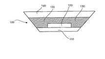
図3は、本発明の実施態様に従った発光装置100の概略図を示している。下から上へ、発光装置100は、基板110と、基板110に取り付けられた底面を有するLED120と、LED120の頂面に配置された封入部材130と、封入部材130上に配置された選択的な補助部材140とを含み、これらの全てはテーパ付き側壁を備えたキャビティ内に置かれている。よって、キャビティは倒立円錐のような形状である。補助部材140は選択的であり、例えば、装置100から放射される光を集束するための光学レンズであり得る。補助部材140は、保護キャップ層としても働き得る。 FIG. 3 shows a schematic diagram of a
明瞭性のために、特定の機能が図3から省略されていることが理解されるであろう。例えば、キャビティの側壁及び基板110は、LED120への電気接続(図示せず)をもたらすより大きなパッケージの一部である。一部の実施態様では、側壁及び基板110を形成するために、キャビティは既存の材料中に定められる。以下により詳細に記載されるように、他の実施態様では、基板110は別個の層であり、キャビティは、基板110の上に結合された1つ又はそれ以上の層内に定められている。 It will be appreciated that certain functions have been omitted from FIG. 3 for clarity. For example, the cavity sidewalls and the
封入部材130は、蛍光材料のような発光材料と、断熱材料とを含む。断熱材料は、発光材料をLED120によって生成される熱から少なくとも部分的に保護し、よって、最適値又はその近傍で、従来技術下よりも一層長く、光変換効率及び出力波長のような熱特性をより良好に維持する。以下に議論されるように、断熱材料は屈折率整合材料でもあることも可能である。 The encapsulating
図3の発光装置100は、封入材料130中の発光材料をLED120によって生成される熱から保護し、且つ、光抽出効率を向上するために、断熱材料を用いることの基本的着想を描写している。先行技術の発光装置(図1及び2)では熱損失が最も重要な関心であったため、それらは蛍光体をLEDによって発生する熱から保護するための断熱を含まないことが理解されよう。言い換えれば、従来技術の発光装置の設計者は、可能な限り多くの熱を蛍光体含有層16,26を通じて放散することを追求した。何故ならば、別なやり方で行うことは、発光装置の残部を通じたより多くの熱損失を必要とするからである。 The
従って、従来技術における焦点は、蛍光体含有層16,26、及び、存在する場合には、スペーサ層15の熱伝導特性を増大することにあり、それはこれらの構造の残余部の限定的な熱伝導特性に起因する。しかしながら、基板110が十分な熱伝導をもたらす場合には、蛍光体含有層16,26を通じて熱を伝導することはもはや不要であり、本発明におけるように、発光材料を保護するために、断熱材を導入し得る。本発明は、そのような可能化基板の実施例を記載するが、本発明は如何なる特定の基板設計又は材料にも限定されないことが理解されよう。 Thus, the focus in the prior art is to increase the heat transfer properties of the phosphor-containing
図3を参照すると、一部の実施態様において、蛍光体材料は断熱材料中に混合されて、混合物を形成し、この混合物は封入材料130を形成する。例えば、多くの一般的に用いられる蛍光体材料は粉末又は顆粒として供給され、これらの粒子は単に断熱材料中に混合或いは分散されて、マトリックスを形成する。このマトリックスで形成された封入部材130は、LED120により接近してというよりも、むしろより離間して位置付けられたこれらの蛍光体粒子のためのより良好な熱保護をもたらすが、一部の用途のために、これは十分であり得る。他の実施態様において、以下に描写されるように、封入部材130は断熱材料及び発光材料の別個の層を含む。 With reference to FIG. 3, in some embodiments, the phosphor material is mixed into a thermal insulating material to form a mixture, which mixture forms an encapsulating
図4は、本発明の他の実施態様に従った発光装置200の概略図である。下から上へ、発光装置200は、基板210と、LED220と、断熱層230と、発光層235と、補助部材240とを含み、これらの全ては倒立円錐の形状を有するテーパ付きキャビティ内に位置付けられている。図3の発光装置100と比べると、発光装置200内の封入部材は、2つの別個の層、即ち、発光材料を含む発光層235と、断熱材料から成る断熱層230とを含む。断熱層230は、発光層235とLED220の頂面との間に配置されている。 FIG. 4 is a schematic diagram of a
図4に示される実施態様は、図3の実施態様に比べ、少なくとも2つの追加的な利益をもたらす。第一に、断熱層230及び発光層235は別々に形成されるので、断熱材料は蛍光体材料のためのホストとして働く適切な特性を有する必要がなく、同様に、発光体材料は断熱材料と適合する必要がない。これは断熱材料及び蛍光体材料の双方のために選択され得る材料の範囲を拡げる。第二に、発光層235は、断熱層230によって、LED220から個別的に分離されているので、発光層235に設けられた熱保護は、発光層235に亘ってより完全であり且つ均一である。 The embodiment shown in FIG. 4 provides at least two additional benefits over the embodiment of FIG. First, since the
発光層235は、断熱層230の外面上に正角に配置されるのが望ましい。これは均一な厚さの発光層235を形成するのに役立つ。発光層235は断熱層230に直接結合されても、或いは、接着剤のような結合剤を用いて断熱層230に結合されてもよい。 The
断熱層230は、LED220から放射される光を通し或いは殆ど通すのが好ましい。従って、断熱材料はLED220によって放射される波長の少なくとも1つを通すのが好ましい。様々な利用可能なLEDによって放射される波長は、LEDの種類に依存して、可視光及び不可視光の双方を含む広域スペクトルに及ぶ。一般的なLEDの波長は概ね約200nm〜2000nmの範囲、即ち、赤外線から紫外線の範囲である。 It is preferable that the
発光層235を効果的に断熱するために、断熱層230の断熱材料は、好ましくは、僅か0.5毎ワット毎メートル毎ケルビン温度(W/m°K)、より望ましくは、僅か0.15毎ワット毎メートル毎ケルビン温度(W/m°K)の低熱伝導率を有するべきである。断熱層230のための断熱材料も、好ましくは、約170℃より高いガラス遷移温度(Tg)、より好ましくは、250℃より高いガラス遷移温度の高熱抵抗を有するのが望ましい。さらに、断熱層230と他の構成部材、特に、典型的には半導体材料であるLED220及び基板210との間の良好な熱適合性及び機械的適合性を有するために、断熱材料は、100ppm/℃程度の熱膨張率を有するのが望ましく、30ppm/℃程度の熱膨張率を有するのがより望ましい。In order to effectively insulate the
さらに、内部全反射を減少するために、断熱層230中の断熱材料は、望ましくは、断熱層230に隣接するLED220の層中の材料の屈折率と類似する屈折率を有するべきである。内部全反射は、LEDの効率に影響を与える重要な要因の1つである。内部全反射の故に、もし入射角がスネルの法則によって決定される臨界角よりも大きいならば、LED220と断熱層230との間の接触面に衝突する光は、LED220内で内部全反射され得る。スネルの法則によれば、2つの隣接する材料の間の屈折率が増大するに応じて臨界角は減少する。従って、屈折率の差が最小限化されるので、臨界角が増大するのに応じて効率が増大する。内部全反射を減少し、従って、LED220の効率を増大するために、断熱材料は1.6よりも大きな屈折率を有するのが望ましく、1.8よりも大きな屈折率を有するのがより望ましく、2.0よりも大きな屈折率をを有するのがより一層望ましい。一部の実施態様において、断熱材料は1.5〜2.1の範囲の屈折率を有する。 Furthermore, in order to reduce total internal reflection, the thermal insulation material in the
本開示に従った断熱層230のための断熱材料として、上記要件を満足する如何なる材料も用い得る。断熱材料は、ポリマー、セラミック、ガラス、及び、これらの混合物、並びに、他の適切な材料を含み得る。具体的な実施例は、Brewer Science,Inc.及びHitachi Chemical Co.,Ltd.によって供給されている高光学品質ポリイミド材料である。これらの商業的に入手可能な高透過性ポリイミド材料の中でも、とりわけ、OptiNDEX B38(Brewer Science)及びPIQ2200(Hitachi Chemical)が、本発明の断熱材料として用いられるのに特に適している。OptiNDEX B38及びPIQ2200は硬化性液体である。硬化後、液状OptiNDEX B38及びPIQ2200は、本発明のために満足できる特性の膜を形成し、本発明の断熱層230を形成するために用い得る。これらのポリイミド材料に関する典型的な特性の一部を表1に列挙する。 Any material that satisfies the above requirements may be used as the thermal insulation material for the

上記のように、一部の実施態様では、断熱材料をスピンコーティングによって塗布し得る。装置を個々に製造するのと対照的に、ウェハレベルで製造するときには、スピンコーティングが望ましい。断熱材料をスピンコーティングによって塗布するとき、断熱材料を4〜40マイクロメートルの範囲内の厚さで蒸着し得る。さらなる処理の後、個々の装置はウェハシンギュレーション(wafer singulation)プロセスによって得られる。 As noted above, in some embodiments, the thermal insulation material may be applied by spin coating. In contrast to manufacturing the devices individually, spin coating is desirable when manufacturing at the wafer level. When the thermal insulation material is applied by spin coating, the thermal insulation material can be deposited at a thickness in the range of 4-40 micrometers. After further processing, the individual devices are obtained by a wafer singulation process.
断熱材料のために上記列挙された特性の多くは、発光層235内又は封入部材130内に発光材料を懸架するために用いられるマトリックスにも当て嵌まることが理解されよう。従って、マトリックス材料は、関連波長で高透過性を有し、且つ、存在するときには、断熱層230の屈折率に密接に適合された、或いは、さもなければ、封入部材130と接触するLED120の層に適合された屈折率を有するのが望ましい。発光層235内で用いられるとき、マトリックス材料は低熱伝導率を有する必要がないのは明らかであるが、断熱層230なしの封入部材130内で用いられるとき、低熱伝導率が必要である。類似の推論がガラス遷移温度に及ぶ。 It will be appreciated that many of the properties listed above for the insulating material also apply to the matrix used to suspend the luminescent material within the
任意の既存のLED及び発光材料を用いて発光装置を作成するために、本発明を用い得る。1つの実施態様において、本発明は単色性のLEDに基づいて白色光を生成し得る光源を提供する。例えば、可視光LED及び補償蛍光体を用いることによって、或いは、RGB蛍光体と一緒に非可視光LEDを用いることによって、これをなし得る。例えば、背景技術の箇所で上記記載されたように、広く用いられている青色LEDに基づく白色光源は、青色光LED、及び、青色光を部分的に吸収した後、黄色光を生成する蛍光体を用いて白色光を生成する。 The present invention can be used to make a light emitting device using any existing LED and light emitting material. In one embodiment, the present invention provides a light source that can generate white light based on a monochromatic LED. This can be done, for example, by using a visible light LED and a compensating phosphor, or by using a non-visible light LED together with an RGB phosphor. For example, as described above in the background section, white light sources based on widely used blue LEDs are blue light LEDs and phosphors that generate yellow light after partially absorbing blue light To generate white light.
本発明に適した発光材料は、蛍光材料(蛍光体)及びリン光性材料の双方を含む。蛍光体はLEDに基づく白色光源のために特に有用である。これらの目的のための一般的な蛍光体は、イットリウムアルミニウムガーネット(YAG)材料、テルビウムアルミニウムガーネット(TAG)材料、ZnSeS+材料、及び、酸窒化ケイ素アルミニウム(SiAlON)材料(例えば、α−SiAlON)を含む。 Luminescent materials suitable for the present invention include both fluorescent materials (phosphors) and phosphorescent materials. Phosphors are particularly useful for white light sources based on LEDs. Common phosphors for these purposes include yttrium aluminum garnet (YAG) material, terbium aluminum garnet (TAG) material, ZnSeS + material, and silicon oxynitride (SiAlON) material (eg, α-SiAlON). Including.
本発明を、図1及び2に関して上述された蛍光層の厚さの均一性を向上するための従来技術の方法を含むLED実装のための様々な方法と組み合わせ得る。一般的に言って、封入材料130は、図1中の層15及び16、並びに、図2中の層26と置換可能である。より具体的には、図1に関して、断熱層230及び発光層235は、それぞれ層15及び16と置換可能であるので、断熱層230は半球形キャップの形状に形成され、且つ、発光層235はそれに合致する。同様に、図2に関して、断熱層230は蛍光体含有層26と置換可能であり、発光層235を断熱層230上に形成し得る。 The present invention may be combined with various methods for LED mounting, including prior art methods for improving the phosphor layer thickness uniformity described above with respect to FIGS. Generally speaking, the encapsulating
具体的には、本発明によれば、高出力LED光源を作成するために、蛍光体をLED発生熱から保護するために断熱材を用いるという着想を、関連出願の箇所で上記列挙された米国仮出願第60/623,266号、第60/623,171号、及び、第60/623,260号に記載されたLEDパッケージと組み合わせ得る。図5乃至7を参照して下述されるように、約1ワット又はそれより高い出力を生成するLED光源を達成し得る。一部の実施態様において、LED光源は約5ワット又はそれより高い出力、約10ワット又はそれより高い出力、及び、約15ワット又はそれより高い出力さえも生成し得る。 Specifically, in accordance with the present invention, the idea of using thermal insulation to protect phosphors from LED generated heat to create a high power LED light source is listed above in the related application section. It can be combined with the LED packages described in provisional applications 60 / 623,266, 60 / 623,171, and 60 / 623,260. As described below with reference to FIGS. 5-7, an LED light source that produces an output of about 1 watt or higher may be achieved. In some embodiments, the LED light source can produce about 5 watts or higher, about 10 watts or higher, and even about 15 watts or higher.
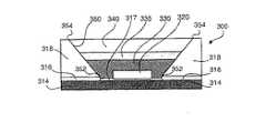
図5及び6は、それぞれ、本発明の実施態様に従った例示的な発光装置300の断面図及び上面図である。図5の断面図から、パッケージの本体が、下から上に指し示された3つの層、即ち、熱伝導層314と、中間本体層316と、上部本体層318とを含むことが分かるであろう。熱伝導層314、中間本体層316、及び、上部本体層318は、全体で、正方形の横断面(図6)と、(内径に対応する)底部リム352から(外径に対応する)頂部リム354へ上方に延在するテーパ付き倒立円錐の形状のキャビティとを備える本体を形成している。キャビティが中間本体層316及び上部本体層318を通じて延在しているのが分かるであろう。LED320、断熱層330、発光層335、及び、選択的な補助部材340を含む他の構成部材もキャビティ内に収容されている。 5 and 6 are a cross-sectional view and a top view, respectively, of an exemplary
図5を参照すると、結合層317がLED320を熱伝導層314の頂面に結合していることが分かる。中間本体層316の厚さは、結合層317の厚さとほぼ同一であるよう設計されている。結合層317は、例えば、導電性エポキシ、はんだ、熱伝導性且つ非導電性エポキシ、又は、ナノカーボン繊維充填接着剤を含み得る。 Referring to FIG. 5, it can be seen that the
本実施態様は、パッケージの4つの隅部のそれぞれに部分ビア(360,362,364,366)も含む。一部の実施態様では、多数の発光装置300が正方形配列で並列に組み立てられ、各部分ビア360,362,364,366は、4つの隣接する発光装置300の間に形成される垂直空孔の4分の1である。垂直空孔の内壁は、メッキ又は他の適切な方法を用いて金属化される。部分ビア360,362,364,366の金属化は電気接続として働く。これらの実施態様では、個々の発光装置300が互いに分離されると、垂直空孔は各個別の発光装置300の部分ビア360,362,364,366になる。 This embodiment also includes partial vias (360, 362, 364, 366) at each of the four corners of the package. In some embodiments, multiple light emitting
図5の実施態様において、キャビティの側壁350は45°の角度で傾斜している。側壁350は、LED320によって放射される波長で極めて反射的な金属化356(図6)のような反射コーティングを有するのが好ましい。例示的な反射コーティングは銀であるが、LED320によって生成される光の波長に依存して、他の材料も用い得る。側壁350は、LED320の端面から放射される光を方向変更する働きをする。LED320の側部から放射される光がLED320の頂面から放射される光を増大するよう、LED320の端面からの光は、LED320の頂面と直交する方向に方向変更される。他の実施態様において、方向変更された光をより良好に集束するよう、側壁350は放物線形状をとる。 In the embodiment of FIG. 5, the
熱伝導層314は高出力LEDから熱を放散するための大幅な利点をもたらすので、発光装置300を過熱させることなく断熱層330を採用し得る。LED320によって発生する熱を効率的に放散するよう、熱伝導層314はLED320の背面に隣接して配置される。熱伝導層314は、以下に記載されるような熱伝導材料から成る。この設計は発光装置300を動作中に多量の熱を発生する高出力LEDに特に適したものにする。 Since the thermally
熱伝導層314が効率的に熱を放散するために、熱伝導層314を作成するために用いられる熱伝導材料は、好ましくは、約200W/m°Kよりも大きな熱伝導率を有するべきである。熱伝導材料は、望ましくは、熱膨張係数及び弾性係数のような適切な熱的及び機械的特性も有するべきである。これらの特性は、望ましくは、発光装置300中の他の構成部材、特に、LED320の半導体材料の特性と適合するべきである。 In order for the thermally
好適実施態様において、熱伝導層314は窒化アルミニウム(AlN)セラミックから成る。1つの実施態様において、熱伝導層314、中間本体層316、及び、上部本体層318は、それぞれAlNセラミックから成る。AlNは高熱伝導率をもたらし、且つ、LED材料の熱膨張係数に近い熱膨張係数を有するので、AlNが望ましい。しかしながら、他の実施態様においては、酸化アルミニウム(Al2O3)をこれらの層のために用い得る。一部の実施態様において、熱伝導層314は、AlN又はAl2O3のいずれかから成るのに対し、中間本体層316及び上部本体層318は、プラスチック、並びに、銅、アルミニウム、Cu/W、及び、合金42を含む他の適切な材料からなる。In the preferred embodiment, the thermally
全ての3つの層がセラミックであるこれらの実施態様において、層を一体に結合するために、一体に積層され且つ共に焼付られた(焼結された)状態で、これらの層を別個に製造し得る。しかしながら、非セラミック材料が中間本体層316及び上部本体層318のために用いられるとき、これらの層を適切な接着剤で一体に結合し得る。 In those embodiments where all three layers are ceramic, these layers are produced separately, laminated together and baked (sintered) together to bond the layers together. obtain. However, when non-ceramic materials are used for the
LED320によって生成される熱は、主として熱伝導層314を通じて、発光装置300のパッケージからヒートシンク(図示せず)に伝達されることが理解されよう。その結果、熱伝導層314は、熱伝導層を通じた熱伝導のために最適化された厚さを有するのが好ましい。もし熱伝導層314が薄過ぎるか或いは厚過ぎるならば熱放散の効率は減少し、従って、最適な熱伝導のための最適な厚さがあることが分かった。これは熱が2つの機構、即ち、面内熱拡散、及び、面を通じた熱転移によって放散されるからである。熱伝導層314が窒化アルミニウム(AlN)から成る実施態様において、推定される最適な厚さは0.2mm〜0.4mmの範囲内である。1つの具体的な実施態様において、厚さは約0.3mmである。 It will be appreciated that the heat generated by the
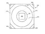
図7は、本発明の他の実施態様に従った発光装置400の上面図である。発光装置400が単一のLEDの代わりに多数のLEDを包含している点を除いて、発光装置400は図6中の発光装置300と類似している。図7に示される具体的な実施態様において、発光装置400は、4つのLED420A,420B,420C,420Dを含む。これらの4つのLEDは、同一であっても相違してもよく、一部の実施態様では、個別に動作可能である。 FIG. 7 is a top view of a
前述の明細書において、本開示は具体的な実施態様を参照して記載されているが、当業者であれば、本開示はそれらに限定されないことを認識するであろう。上記に記載の様々な機能及び特徴を個別に又は一緒に用い得る。さらに、明細書のより広い精神及び範囲から逸脱することなく、ここに記載されたものを超えて、本開示を如何なる数の環境及び用途に利用し得る。従って、明細書及び図面は制限的というよりもむしろ例示的と考えられるべきである。ここで用いられている「含む」、「包含する」、及び、「有する」という用語は、制約のない技術用語として読み取られるべきことが特に意図されている。 In the foregoing specification, the disclosure has been described with reference to specific embodiments, but those skilled in the art will recognize that the disclosure is not limited thereto. The various functions and features described above may be used individually or together. Further, the present disclosure may be utilized in any number of environments and applications beyond what is described herein without departing from the broader spirit and scope of the specification. Accordingly, the specification and drawings are to be regarded as illustrative rather than restrictive. It is specifically intended that the terms “include”, “include” and “have” as used herein should be read as unrestricted technical terms.
10 発光装置
12 LED
14 基板
15 スペーサ層
16 発光体含有層
20 発光装置
22 LED
24 基板
26 発光体含有層
100 発光装置
110 基板
120 LED
130 封入部材
140 補助部材
200 発光装置
210 基板
220 LED
230 断熱層
235 発光層
240 補助部材
300 発光装置
314 熱伝導層
316 中間本体層
317 結合層
318 上部本体層
320 LED
330 断熱層
335 発光層
340 補助部材
350 側壁
352 底部リム
354 頂部リム
356 金属化
360,362,364,366 部分ビア
420A,420B,420C,420D LED10 Light-emitting
14
24
130 Encapsulating
230
330
Claims (45)
Translated fromJapanese該発光ダイオードの頂面を被覆する封入部材とを含み、
該封入部材は、発光材料及び断熱材料を含む、
発光装置。A light emitting diode;
An encapsulating member covering the top surface of the light emitting diode;
The encapsulating member includes a light emitting material and a heat insulating material.
Light emitting device.
該熱伝導層に結合された発光ダイオードと、
該発光ダイオードの上に配置された断熱材料と、
該断熱材料の上に配置された発光材料と、
を含む発光ダイオードパッケージ。A thermally conductive layer made of a thermally conductive material having a thermal conductivity greater than 200 W / m ° K;
A light emitting diode coupled to the thermally conductive layer;
A heat insulating material disposed on the light emitting diode;
A light emitting material disposed on the heat insulating material;
Including light emitting diode package.
該熱伝導層に結合された発光ダイオードと、
該発光ダイオードの頂面を被覆する封入部材とを含み、
該封入部材は、発光材料及び断熱材料を含む、
1ワット又はそれより大きな出力を生成するための発光ダイオードパッケージ。A heat conducting layer comprising a heat conducting ceramic having a thermal conductivity greater than 200 W / m ° K;
A light emitting diode coupled to the thermally conductive layer;
An encapsulating member covering the top surface of the light emitting diode;
The encapsulating member includes a light emitting material and a heat insulating material.
Light emitting diode package for producing 1 watt or greater output.
Applications Claiming Priority (4)
| Application Number | Priority Date | Filing Date | Title |
|---|---|---|---|
| US62326004P | 2004-10-29 | 2004-10-29 | |
| US62317104P | 2004-10-29 | 2004-10-29 | |
| US62326604P | 2004-10-29 | 2004-10-29 | |
| US11/036,559US8134292B2 (en) | 2004-10-29 | 2005-01-13 | Light emitting device with a thermal insulating and refractive index matching material |
Publications (1)
| Publication Number | Publication Date |
|---|---|
| JP2006128700Atrue JP2006128700A (en) | 2006-05-18 |
Family
ID=36261019
Family Applications (1)
| Application Number | Title | Priority Date | Filing Date |
|---|---|---|---|
| JP2005315149APendingJP2006128700A (en) | 2004-10-29 | 2005-10-28 | Light emitting device with thermal insulation and refractive index matching material |
Country Status (3)
| Country | Link |
|---|---|
| US (1) | US8134292B2 (en) |
| JP (1) | JP2006128700A (en) |
| TW (4) | TWI298208B (en) |
Cited By (11)
| Publication number | Priority date | Publication date | Assignee | Title |
|---|---|---|---|---|
| JP2007194525A (en)* | 2006-01-23 | 2007-08-02 | Matsushita Electric Ind Co Ltd | Semiconductor light emitting device |
| JP2008028100A (en)* | 2006-07-20 | 2008-02-07 | Lumi Tech:Kk | Light-emitting device |
| JP2010514187A (en)* | 2006-12-21 | 2010-04-30 | コーニンクレッカ フィリップス エレクトロニクス エヌ ヴィ | Light emitting device having tangible wavelength converter |
| WO2010123059A1 (en)* | 2009-04-22 | 2010-10-28 | シーシーエス株式会社 | Method for manufacturing led light emitting device |
| JP2011503892A (en)* | 2007-11-20 | 2011-01-27 | コーニンクレッカ フィリップス エレクトロニクス エヌ ヴィ | Collimated light emitting device and method |
| KR101308774B1 (en) | 2006-09-20 | 2013-09-17 | 가부시키가이샤 니콘 | Method of manufacturing an optical element and a resin-sealed light emitting element, the optical element, the resin-sealed light emitting element, and a planar light source device |
| KR101396585B1 (en)* | 2007-06-11 | 2014-05-20 | 서울반도체 주식회사 | Light emitting diode package having composite material layer incorporating carbon nano material |
| JP2015015485A (en)* | 2008-11-28 | 2015-01-22 | 株式会社小糸製作所 | Light emitting module, and lighting fixture unit |
| KR101538224B1 (en)* | 2013-10-11 | 2015-07-22 | 이주혁 | Led lamp |
| JP5750538B1 (en)* | 2014-09-03 | 2015-07-22 | 四国計測工業株式会社 | LED light emitting device |
| WO2017221777A1 (en)* | 2016-06-21 | 2017-12-28 | 東レ株式会社 | Light-emitting body, light source unit in which same is used, display, and illumination device |
Families Citing this family (92)
| Publication number | Priority date | Publication date | Assignee | Title |
|---|---|---|---|---|
| US7915085B2 (en) | 2003-09-18 | 2011-03-29 | Cree, Inc. | Molded chip fabrication method |
| US7837348B2 (en) | 2004-05-05 | 2010-11-23 | Rensselaer Polytechnic Institute | Lighting system using multiple colored light emitting sources and diffuser element |
| AU2005240186B2 (en)* | 2004-05-05 | 2011-02-03 | Rensselaer Polytechnic Institute | High efficiency light source using solid-state emitter and down-conversion material |
| US8816369B2 (en) | 2004-10-29 | 2014-08-26 | Led Engin, Inc. | LED packages with mushroom shaped lenses and methods of manufacturing LED light-emitting devices |
| US9929326B2 (en) | 2004-10-29 | 2018-03-27 | Ledengin, Inc. | LED package having mushroom-shaped lens with volume diffuser |
| JP4634810B2 (en)* | 2005-01-20 | 2011-02-16 | 信越化学工業株式会社 | Silicone sealed LED |
| CA2597697C (en)* | 2005-06-23 | 2014-12-02 | Rensselaer Polytechnic Institute | Package design for producing white light with short-wavelength leds and down-conversion materials |
| DE102005034793B3 (en)* | 2005-07-21 | 2007-04-19 | G.L.I. Global Light Industries Gmbh | Light-emitting semiconductor diode of high light output |
| DE102005044347A1 (en)* | 2005-09-16 | 2007-03-22 | BSH Bosch und Siemens Hausgeräte GmbH | Lighting device for ovens and ovens |
| KR20070033801A (en)* | 2005-09-22 | 2007-03-27 | 삼성전기주식회사 | Light emitting diode package and manufacturing method thereof |
| JP4952884B2 (en)* | 2006-01-24 | 2012-06-13 | ソニー株式会社 | Semiconductor light emitting device and semiconductor light emitting device assembly |
| US8969908B2 (en) | 2006-04-04 | 2015-03-03 | Cree, Inc. | Uniform emission LED package |
| US20070241661A1 (en)* | 2006-04-12 | 2007-10-18 | Yin Chua B | High light output lamps having a phosphor embedded glass/ceramic layer |
| US7943952B2 (en) | 2006-07-31 | 2011-05-17 | Cree, Inc. | Method of uniform phosphor chip coating and LED package fabricated using method |
| US7703942B2 (en)* | 2006-08-31 | 2010-04-27 | Rensselaer Polytechnic Institute | High-efficient light engines using light emitting diodes |
| US10295147B2 (en) | 2006-11-09 | 2019-05-21 | Cree, Inc. | LED array and method for fabricating same |
| US7889421B2 (en) | 2006-11-17 | 2011-02-15 | Rensselaer Polytechnic Institute | High-power white LEDs and manufacturing method thereof |
| JP2010512662A (en) | 2006-12-11 | 2010-04-22 | ザ リージェンツ オブ ザ ユニバーシティ オブ カリフォルニア | Transparent light emitting diode |
| US9159888B2 (en) | 2007-01-22 | 2015-10-13 | Cree, Inc. | Wafer level phosphor coating method and devices fabricated utilizing method |
| US9024349B2 (en) | 2007-01-22 | 2015-05-05 | Cree, Inc. | Wafer level phosphor coating method and devices fabricated utilizing method |
| US8232564B2 (en) | 2007-01-22 | 2012-07-31 | Cree, Inc. | Wafer level phosphor coating technique for warm light emitting diodes |
| EP2120271A4 (en)* | 2007-03-01 | 2015-03-25 | Nec Lighting Ltd | LED ARRANGEMENT AND LIGHTING DEVICE |
| TW200837982A (en)* | 2007-03-07 | 2008-09-16 | Everlight Electronics Co Ltd | Semiconductor light emitting apparatus and the manufacturing method thereof |
| KR100883074B1 (en)* | 2007-03-21 | 2009-02-10 | 엘지전자 주식회사 | Electroluminescent element |
| US10505083B2 (en) | 2007-07-11 | 2019-12-10 | Cree, Inc. | Coating method utilizing phosphor containment structure and devices fabricated using same |
| TW200924232A (en)* | 2007-11-26 | 2009-06-01 | Lin Pin Ya | Light emitting diode capable of radiating light and dissipating heat in dual directions |
| US9041285B2 (en) | 2007-12-14 | 2015-05-26 | Cree, Inc. | Phosphor distribution in LED lamps using centrifugal force |
| US8167674B2 (en) | 2007-12-14 | 2012-05-01 | Cree, Inc. | Phosphor distribution in LED lamps using centrifugal force |
| US8878219B2 (en) | 2008-01-11 | 2014-11-04 | Cree, Inc. | Flip-chip phosphor coating method and devices fabricated utilizing method |
| US10008637B2 (en) | 2011-12-06 | 2018-06-26 | Cree, Inc. | Light emitter devices and methods with reduced dimensions and improved light output |
| US8637883B2 (en)* | 2008-03-19 | 2014-01-28 | Cree, Inc. | Low index spacer layer in LED devices |
| DE102009018087A1 (en) | 2008-04-30 | 2009-12-17 | Ledon Lighting Jennersdorf Gmbh | Light-emitting diode with increased color stability |
| US8075165B2 (en)* | 2008-10-14 | 2011-12-13 | Ledengin, Inc. | Total internal reflection lens and mechanical retention and locating device |
| JP5440064B2 (en)* | 2008-10-21 | 2014-03-12 | 東芝ライテック株式会社 | Lighting device |
| US20110257488A1 (en)* | 2008-10-31 | 2011-10-20 | Limited Liability Company Japan Medical Creative | Surgical lighting system |
| US20100117106A1 (en)* | 2008-11-07 | 2010-05-13 | Ledengin, Inc. | Led with light-conversion layer |
| KR20100087851A (en)* | 2009-01-29 | 2010-08-06 | 삼성전자주식회사 | Light-emitting unit, method of manufacturing the same, and light source device having the light-emitting unit |
| US8507300B2 (en)* | 2008-12-24 | 2013-08-13 | Ledengin, Inc. | Light-emitting diode with light-conversion layer |
| TWI573299B (en)* | 2008-12-31 | 2017-03-01 | 榮創能源科技股份有限公司 | Compound semiconductor device package module structure and fabricating method thereof |
| US7985000B2 (en)* | 2009-04-08 | 2011-07-26 | Ledengin, Inc. | Lighting apparatus having multiple light-emitting diodes with individual light-conversion layers |
| US8598793B2 (en) | 2011-05-12 | 2013-12-03 | Ledengin, Inc. | Tuning of emitter with multiple LEDs to a single color bin |
| CN101894901B (en) | 2009-04-08 | 2013-11-20 | 硅谷光擎 | Package for multiple light emitting diodes |
| DE102009053064A1 (en)* | 2009-11-13 | 2011-05-19 | Osram Opto Semiconductors Gmbh | Protective diode structure thin film semiconductor device and method of fabricating a thin film semiconductor device |
| TWI381563B (en)* | 2009-11-20 | 2013-01-01 | Everlight Electronics Co Ltd | Light emitting diode package and manufacturing method thereof |
| TWI398215B (en)* | 2009-12-14 | 2013-06-01 | Pegatron Corp | Casing and manufacturing method thereof |
| US8303141B2 (en)* | 2009-12-17 | 2012-11-06 | Ledengin, Inc. | Total internal reflection lens with integrated lamp cover |
| JP5047264B2 (en) | 2009-12-22 | 2012-10-10 | 株式会社東芝 | Light emitting device |
| US8384105B2 (en)* | 2010-03-19 | 2013-02-26 | Micron Technology, Inc. | Light emitting diodes with enhanced thermal sinking and associated methods of operation |
| US8598612B2 (en) | 2010-03-30 | 2013-12-03 | Micron Technology, Inc. | Light emitting diode thermally enhanced cavity package and method of manufacture |
| US9345095B2 (en) | 2010-04-08 | 2016-05-17 | Ledengin, Inc. | Tunable multi-LED emitter module |
| US8858022B2 (en) | 2011-05-05 | 2014-10-14 | Ledengin, Inc. | Spot TIR lens system for small high-power emitter |
| TWI402460B (en)* | 2010-04-09 | 2013-07-21 | Biao Qin | LED wick and LED chip and manufacturing method |
| DE102010021791A1 (en) | 2010-05-27 | 2011-12-01 | Osram Opto Semiconductors Gmbh | Optoelectronic component and method for producing an optoelectronic component and a composite |
| US10546846B2 (en) | 2010-07-23 | 2020-01-28 | Cree, Inc. | Light transmission control for masking appearance of solid state light sources |
| DE102010042217A1 (en)* | 2010-10-08 | 2012-04-12 | Osram Ag | Optoelectronic semiconductor component and method for its production |
| US9166126B2 (en) | 2011-01-31 | 2015-10-20 | Cree, Inc. | Conformally coated light emitting devices and methods for providing the same |
| TWI473305B (en)* | 2011-03-10 | 2015-02-11 | Formosa Epitaxy Inc | Light emitting diode structure |
| US20120250320A1 (en)* | 2011-03-31 | 2012-10-04 | Xicato, Inc. | Color conversion cavities for led-based illumination modules |
| DE102011016567B4 (en)* | 2011-04-08 | 2023-05-11 | OSRAM Opto Semiconductors Gesellschaft mit beschränkter Haftung | Method for producing an optoelectronic component and component produced in this way |
| US8513900B2 (en) | 2011-05-12 | 2013-08-20 | Ledengin, Inc. | Apparatus for tuning of emitter with multiple LEDs to a single color bin |
| DE102011105010A1 (en)* | 2011-06-20 | 2012-12-20 | Osram Opto Semiconductors Gmbh | Optoelectronic semiconductor component and method for its production |
| US10686107B2 (en) | 2011-07-21 | 2020-06-16 | Cree, Inc. | Light emitter devices and components with improved chemical resistance and related methods |
| JP2014525146A (en) | 2011-07-21 | 2014-09-25 | クリー インコーポレイテッド | Light emitting device, package, component, and method for improved chemical resistance and related methods |
| US10211380B2 (en) | 2011-07-21 | 2019-02-19 | Cree, Inc. | Light emitting devices and components having improved chemical resistance and related methods |
| CN102956761B (en)* | 2011-08-25 | 2015-03-11 | 展晶科技(深圳)有限公司 | Method for packaging light emitting diode |
| EP2786429A4 (en)* | 2011-12-01 | 2015-07-29 | Cree Inc | LIGHT EMITTING DEVICES AND COMPONENTS HAVING ENHANCED CHEMICAL RESISTANCE AND RELATED METHODS |
| US11032884B2 (en) | 2012-03-02 | 2021-06-08 | Ledengin, Inc. | Method for making tunable multi-led emitter module |
| US9897284B2 (en) | 2012-03-28 | 2018-02-20 | Ledengin, Inc. | LED-based MR16 replacement lamp |
| CN102916116B (en)* | 2012-08-14 | 2015-11-25 | 纳晶科技股份有限公司 | LED optical accessory, LED and LED optical accessory preparation method |
| US9557215B2 (en)* | 2012-08-17 | 2017-01-31 | Massachusetts Institute Of Technology | Phonon-recyling light-emitting diodes |
| TWI502733B (en)* | 2012-11-02 | 2015-10-01 | 環旭電子股份有限公司 | Electronic package module and method of manufacturing the same |
| KR102006390B1 (en)* | 2013-03-11 | 2019-08-01 | 삼성전자주식회사 | Method of manufacturing Light Emitting diode package |
| US9234801B2 (en) | 2013-03-15 | 2016-01-12 | Ledengin, Inc. | Manufacturing method for LED emitter with high color consistency |
| US20140367816A1 (en)* | 2013-06-12 | 2014-12-18 | Avago Technologies General Ip (Singapore) Pte.Ltd. | Photodetector device having light-collecting optical microstructure |
| EP3033776A4 (en) | 2013-08-16 | 2017-01-25 | Massachusetts Institute of Technology | Thermo-electrically pumped light-emitting diodes |
| US9406654B2 (en) | 2014-01-27 | 2016-08-02 | Ledengin, Inc. | Package for high-power LED devices |
| JP6252302B2 (en)* | 2014-03-28 | 2017-12-27 | 日亜化学工業株式会社 | Method for manufacturing light emitting device |
| DE102014112883A1 (en)* | 2014-09-08 | 2016-03-10 | Osram Opto Semiconductors Gmbh | Optoelectronic component |
| CN107004677B (en) | 2014-11-26 | 2020-08-25 | 硅谷光擎 | Compact transmitter for warm dimming and color-tunable lamps |
| KR102252994B1 (en)* | 2014-12-18 | 2021-05-20 | 삼성전자주식회사 | Light emitting device package and fluorescent film for the same |
| US9530943B2 (en) | 2015-02-27 | 2016-12-27 | Ledengin, Inc. | LED emitter packages with high CRI |
| CN105226186B (en)* | 2015-10-10 | 2018-06-01 | 深圳市华星光电技术有限公司 | The production method of flexible display apparatus and flexible display apparatus obtained |
| CN106848031A (en) | 2015-12-04 | 2017-06-13 | 财团法人工业技术研究院 | Packaging structure of ultraviolet light emitting diode |
| DE102016203162A1 (en)* | 2016-02-29 | 2017-08-31 | Tridonic Jennersdorf Gmbh | CSP LED module with improved light emission |
| WO2017151730A1 (en)* | 2016-03-01 | 2017-09-08 | Exergy Dynamics, Inc. | Light emitting diode assemblies utilizing heat sharing from light-conditioning structures for enhanced energy efficiency |
| TWI696300B (en) | 2016-03-15 | 2020-06-11 | 晶元光電股份有限公司 | A light-emitting device and the manufacturing method thereof |
| TWI837362B (en)* | 2016-03-15 | 2024-04-01 | 晶元光電股份有限公司 | A light-emitting module |
| DE102016106833A1 (en) | 2016-04-13 | 2017-10-19 | Osram Opto Semiconductors Gmbh | Component with reflector and method for the production of components |
| US10219345B2 (en) | 2016-11-10 | 2019-02-26 | Ledengin, Inc. | Tunable LED emitter with continuous spectrum |
| CN207969020U (en)* | 2018-02-06 | 2018-10-12 | 广东欧曼科技股份有限公司 | Low-pressure lamp band |
| US10575374B2 (en) | 2018-03-09 | 2020-02-25 | Ledengin, Inc. | Package for flip-chip LEDs with close spacing of LED chips |
| CN109301056B (en)* | 2018-09-30 | 2020-05-19 | 京东方科技集团股份有限公司 | A kind of LED light source and preparation method thereof, backlight source, display device |
Citations (5)
| Publication number | Priority date | Publication date | Assignee | Title |
|---|---|---|---|---|
| JP2000349346A (en)* | 1999-06-07 | 2000-12-15 | Sanken Electric Co Ltd | Semiconductor light emitting device |
| JP2000349347A (en)* | 1999-06-08 | 2000-12-15 | Sanken Electric Co Ltd | Semiconductor light emitting element |
| JP2001057445A (en)* | 1999-08-19 | 2001-02-27 | Rohm Co Ltd | Light-emitting diode |
| JP2002185046A (en)* | 2000-12-19 | 2002-06-28 | Sharp Corp | Chip component type LED and method of manufacturing the same |
| JP2004241704A (en)* | 2003-02-07 | 2004-08-26 | Shin Etsu Chem Co Ltd | Light emitting device and manufacturing method thereof |
Family Cites Families (71)
| Publication number | Priority date | Publication date | Assignee | Title |
|---|---|---|---|---|
| US5742120A (en)* | 1996-05-10 | 1998-04-21 | Rebif Corporation | Light-emmiting diode lamp with directional coverage for the emmitted light |
| DE19638667C2 (en)* | 1996-09-20 | 2001-05-17 | Osram Opto Semiconductors Gmbh | Mixed-color light-emitting semiconductor component with luminescence conversion element |
| US6608332B2 (en)* | 1996-07-29 | 2003-08-19 | Nichia Kagaku Kogyo Kabushiki Kaisha | Light emitting device and display |
| TW383508B (en)* | 1996-07-29 | 2000-03-01 | Nichia Kagaku Kogyo Kk | Light emitting device and display |
| DE19748240C2 (en)* | 1997-10-31 | 2001-05-23 | Fraunhofer Ges Forschung | Process for the corrosion-resistant coating of metal substrates by means of plasma polymerization and its application |
| DE19755734A1 (en)* | 1997-12-15 | 1999-06-24 | Siemens Ag | Method for producing a surface-mountable optoelectronic component |
| TW542932B (en)* | 1998-02-09 | 2003-07-21 | Seiko Epson Corp | Liquid crystal panel and electronic appliances |
| US5959316A (en)* | 1998-09-01 | 1999-09-28 | Hewlett-Packard Company | Multiple encapsulation of phosphor-LED devices |
| US6335548B1 (en)* | 1999-03-15 | 2002-01-01 | Gentex Corporation | Semiconductor radiation emitter package |
| US6307160B1 (en)* | 1998-10-29 | 2001-10-23 | Agilent Technologies, Inc. | High-strength solder interconnect for copper/electroless nickel/immersion gold metallization solder pad and method |
| US6351069B1 (en)* | 1999-02-18 | 2002-02-26 | Lumileds Lighting, U.S., Llc | Red-deficiency-compensating phosphor LED |
| US6737801B2 (en)* | 2000-06-28 | 2004-05-18 | The Fox Group, Inc. | Integrated color LED chip |
| AT410266B (en)* | 2000-12-28 | 2003-03-25 | Tridonic Optoelectronics Gmbh | LIGHT SOURCE WITH A LIGHT-EMITTING ELEMENT |
| US6949771B2 (en)* | 2001-04-25 | 2005-09-27 | Agilent Technologies, Inc. | Light source |
| US6642652B2 (en)* | 2001-06-11 | 2003-11-04 | Lumileds Lighting U.S., Llc | Phosphor-converted light emitting device |
| JP4114331B2 (en)* | 2001-06-15 | 2008-07-09 | 豊田合成株式会社 | Light emitting device |
| US20020191885A1 (en)* | 2001-06-18 | 2002-12-19 | Chi Wu | Optical component having improved warping symmetry |
| US20030016899A1 (en)* | 2001-06-18 | 2003-01-23 | Xiantao Yan | Optical components with controlled temperature sensitivity |
| DE10131698A1 (en)* | 2001-06-29 | 2003-01-30 | Osram Opto Semiconductors Gmbh | Surface-mountable radiation-emitting component and method for its production |
| US6680128B2 (en)* | 2001-09-27 | 2004-01-20 | Agilent Technologies, Inc. | Method of making lead-free solder and solder paste with improved wetting and shelf life |
| US20030086674A1 (en)* | 2001-11-05 | 2003-05-08 | Xiantao Yan | Optical components with reduced temperature sensitivity |
| US6948840B2 (en)* | 2001-11-16 | 2005-09-27 | Everbrite, Llc | Light emitting diode light bar |
| KR100439402B1 (en)* | 2001-12-24 | 2004-07-09 | 삼성전기주식회사 | Light emission diode package |
| WO2003065464A1 (en)* | 2002-01-28 | 2003-08-07 | Nichia Corporation | Nitride semiconductor device having support substrate and its manufacturing method |
| US6791116B2 (en)* | 2002-04-30 | 2004-09-14 | Toyoda Gosei Co., Ltd. | Light emitting diode |
| US6870311B2 (en)* | 2002-06-07 | 2005-03-22 | Lumileds Lighting U.S., Llc | Light-emitting devices utilizing nanoparticles |
| US20030230977A1 (en)* | 2002-06-12 | 2003-12-18 | Epstein Howard C. | Semiconductor light emitting device with fluoropolymer lens |
| JP3761501B2 (en)* | 2002-07-31 | 2006-03-29 | 本多通信工業株式会社 | Coaxial connector and ground pad on which it is mounted |
| US7244965B2 (en)* | 2002-09-04 | 2007-07-17 | Cree Inc, | Power surface mount light emitting die package |
| US7264378B2 (en)* | 2002-09-04 | 2007-09-04 | Cree, Inc. | Power surface mount light emitting die package |
| JP2004153241A (en)* | 2002-10-11 | 2004-05-27 | Sharp Corp | Semiconductor light emitting device and method of manufacturing the same |
| JP2004140185A (en)* | 2002-10-17 | 2004-05-13 | Matsushita Electric Ind Co Ltd | Light emitting device |
| US7168608B2 (en)* | 2002-12-24 | 2007-01-30 | Avago Technologies General Ip (Singapore) Pte. Ltd. | System and method for hermetic seal formation |
| JP2004253404A (en) | 2002-12-24 | 2004-09-09 | Kyocera Corp | Light emitting element storage package and light emitting device |
| US7199446B1 (en)* | 2003-02-18 | 2007-04-03 | K2 Optronics, Inc. | Stacked electrical resistor pad for optical fiber attachment |
| US6835960B2 (en)* | 2003-03-03 | 2004-12-28 | Opto Tech Corporation | Light emitting diode package structure |
| JP2004273798A (en)* | 2003-03-10 | 2004-09-30 | Toyoda Gosei Co Ltd | Light emitting device |
| WO2004081140A1 (en)* | 2003-03-13 | 2004-09-23 | Nichia Corporation | Light emitting film, luminescent device, method for manufacturing light emitting film and method for manufacturing luminescent device |
| US6903380B2 (en)* | 2003-04-11 | 2005-06-07 | Weldon Technologies, Inc. | High power light emitting diode |
| US7157745B2 (en)* | 2004-04-09 | 2007-01-02 | Blonder Greg E | Illumination devices comprising white light emitting diodes and diode arrays and method and apparatus for making them |
| WO2004114001A1 (en)* | 2003-06-20 | 2004-12-29 | Casio Computer Co., Ltd. | Display device and manufacturing method of the same |
| DE102004034166B4 (en)* | 2003-07-17 | 2015-08-20 | Toyoda Gosei Co., Ltd. | Light-emitting device |
| US7157744B2 (en)* | 2003-10-29 | 2007-01-02 | M/A-Com, Inc. | Surface mount package for a high power light emitting diode |
| JP4792726B2 (en)* | 2003-10-30 | 2011-10-12 | 日亜化学工業株式会社 | Manufacturing method of support for semiconductor element |
| JP4557542B2 (en)* | 2003-12-24 | 2010-10-06 | ▲さん▼圓光電股▲ふん▼有限公司 | Nitride light emitting device and high luminous efficiency nitride light emitting device |
| US7675231B2 (en)* | 2004-02-13 | 2010-03-09 | Avago Technologies Ecbu Ip (Singapore) Pte. Ltd. | Light emitting diode display device comprising a high temperature resistant overlay |
| TWI240423B (en)* | 2004-03-12 | 2005-09-21 | Opto Tech Corp | Light emitting device with high heat dissipation efficiency |
| US7517728B2 (en)* | 2004-03-31 | 2009-04-14 | Cree, Inc. | Semiconductor light emitting devices including a luminescent conversion element |
| US7868343B2 (en)* | 2004-04-06 | 2011-01-11 | Cree, Inc. | Light-emitting devices having multiple encapsulation layers with at least one of the encapsulation layers including nanoparticles and methods of forming the same |
| US7012328B2 (en)* | 2004-05-14 | 2006-03-14 | Intevac, Inc. | Semiconductor die attachment for high vacuum tubes |
| US7064353B2 (en)* | 2004-05-26 | 2006-06-20 | Philips Lumileds Lighting Company, Llc | LED chip with integrated fast switching diode for ESD protection |
| US7280288B2 (en)* | 2004-06-04 | 2007-10-09 | Cree, Inc. | Composite optical lens with an integrated reflector |
| US7167309B2 (en)* | 2004-06-25 | 2007-01-23 | Northrop Grumman Corporation | Optical compensation of cover glass-air gap-display stack for high ambient lighting |
| KR100674827B1 (en)* | 2004-07-28 | 2007-01-25 | 삼성전기주식회사 | LED package for backlight unit |
| US7405093B2 (en)* | 2004-08-18 | 2008-07-29 | Cree, Inc. | Methods of assembly for a semiconductor light emitting device package |
| US20060082296A1 (en)* | 2004-10-14 | 2006-04-20 | Chua Janet Bee Y | Mixture of alkaline earth metal thiogallate green phosphor and sulfide red phosphor for phosphor-converted LED |
| US7679672B2 (en)* | 2004-10-14 | 2010-03-16 | Avago Technologies Ecbu Ip (Singapore) Pte. Ltd. | Electronic flash, imaging device and method for producing a flash of light having a wavelength spectrum in the visible range and the infrared range using a fluorescent material |
| US20060097385A1 (en)* | 2004-10-25 | 2006-05-11 | Negley Gerald H | Solid metal block semiconductor light emitting device mounting substrates and packages including cavities and heat sinks, and methods of packaging same |
| US7452737B2 (en)* | 2004-11-15 | 2008-11-18 | Philips Lumileds Lighting Company, Llc | Molded lens over LED die |
| US7352011B2 (en)* | 2004-11-15 | 2008-04-01 | Philips Lumileds Lighting Company, Llc | Wide emitting lens for LED useful for backlighting |
| US7858408B2 (en)* | 2004-11-15 | 2010-12-28 | Koninklijke Philips Electronics N.V. | LED with phosphor tile and overmolded phosphor in lens |
| US7344902B2 (en)* | 2004-11-15 | 2008-03-18 | Philips Lumileds Lighting Company, Llc | Overmolded lens over LED die |
| KR20060132298A (en)* | 2005-06-17 | 2006-12-21 | 삼성전기주식회사 | Light emitting device package |
| WO2007002342A2 (en)* | 2005-06-22 | 2007-01-04 | Nextreme Thermal Solutions | Methods of forming thermoelectric devices including electrically insulating matrixes between conductive traces and related structures |
| US7646035B2 (en)* | 2006-05-31 | 2010-01-12 | Cree, Inc. | Packaged light emitting devices including multiple index lenses and multiple index lenses for packaged light emitting devices |
| US7479660B2 (en)* | 2005-10-21 | 2009-01-20 | Perkinelmer Elcos Gmbh | Multichip on-board LED illumination device |
| KR100665375B1 (en)* | 2006-02-22 | 2007-01-09 | 삼성전기주식회사 | LED Package |
| TWI358575B (en)* | 2006-03-17 | 2012-02-21 | Light diffusion reflection sheet with buffering ef | |
| JP2007273562A (en)* | 2006-03-30 | 2007-10-18 | Toshiba Corp | Semiconductor light emitting device |
| US8044418B2 (en)* | 2006-07-13 | 2011-10-25 | Cree, Inc. | Leadframe-based packages for solid state light emitting devices |
| US7999283B2 (en)* | 2007-06-14 | 2011-08-16 | Cree, Inc. | Encapsulant with scatterer to tailor spatial emission pattern and color uniformity in light emitting diodes |
- 2005
- 2005-01-13USUS11/036,559patent/US8134292B2/enactiveActive
- 2005-10-05TWTW094134804Apatent/TWI298208B/enactive
- 2005-10-28TWTW094137992Apatent/TWI373855B/enactive
- 2005-10-28JPJP2005315149Apatent/JP2006128700A/enactivePending
- 2005-10-28TWTW094137990Apatent/TWI277227B/enactive
- 2005-10-28TWTW094137991Apatent/TWI270993B/enactive
Patent Citations (5)
| Publication number | Priority date | Publication date | Assignee | Title |
|---|---|---|---|---|
| JP2000349346A (en)* | 1999-06-07 | 2000-12-15 | Sanken Electric Co Ltd | Semiconductor light emitting device |
| JP2000349347A (en)* | 1999-06-08 | 2000-12-15 | Sanken Electric Co Ltd | Semiconductor light emitting element |
| JP2001057445A (en)* | 1999-08-19 | 2001-02-27 | Rohm Co Ltd | Light-emitting diode |
| JP2002185046A (en)* | 2000-12-19 | 2002-06-28 | Sharp Corp | Chip component type LED and method of manufacturing the same |
| JP2004241704A (en)* | 2003-02-07 | 2004-08-26 | Shin Etsu Chem Co Ltd | Light emitting device and manufacturing method thereof |
Cited By (12)
| Publication number | Priority date | Publication date | Assignee | Title |
|---|---|---|---|---|
| JP2007194525A (en)* | 2006-01-23 | 2007-08-02 | Matsushita Electric Ind Co Ltd | Semiconductor light emitting device |
| JP2008028100A (en)* | 2006-07-20 | 2008-02-07 | Lumi Tech:Kk | Light-emitting device |
| KR101308774B1 (en) | 2006-09-20 | 2013-09-17 | 가부시키가이샤 니콘 | Method of manufacturing an optical element and a resin-sealed light emitting element, the optical element, the resin-sealed light emitting element, and a planar light source device |
| JP2010514187A (en)* | 2006-12-21 | 2010-04-30 | コーニンクレッカ フィリップス エレクトロニクス エヌ ヴィ | Light emitting device having tangible wavelength converter |
| KR101396585B1 (en)* | 2007-06-11 | 2014-05-20 | 서울반도체 주식회사 | Light emitting diode package having composite material layer incorporating carbon nano material |
| JP2011503892A (en)* | 2007-11-20 | 2011-01-27 | コーニンクレッカ フィリップス エレクトロニクス エヌ ヴィ | Collimated light emitting device and method |
| JP2015015485A (en)* | 2008-11-28 | 2015-01-22 | 株式会社小糸製作所 | Light emitting module, and lighting fixture unit |
| WO2010123059A1 (en)* | 2009-04-22 | 2010-10-28 | シーシーエス株式会社 | Method for manufacturing led light emitting device |
| JPWO2010123059A1 (en)* | 2009-04-22 | 2012-10-25 | シーシーエス株式会社 | Manufacturing method of LED light emitting device |
| KR101538224B1 (en)* | 2013-10-11 | 2015-07-22 | 이주혁 | Led lamp |
| JP5750538B1 (en)* | 2014-09-03 | 2015-07-22 | 四国計測工業株式会社 | LED light emitting device |
| WO2017221777A1 (en)* | 2016-06-21 | 2017-12-28 | 東レ株式会社 | Light-emitting body, light source unit in which same is used, display, and illumination device |
Also Published As
| Publication number | Publication date |
|---|---|
| TW200620716A (en) | 2006-06-16 |
| TW200633261A (en) | 2006-09-16 |
| TWI373855B (en) | 2012-10-01 |
| US20060091788A1 (en) | 2006-05-04 |
| TWI277227B (en) | 2007-03-21 |
| US8134292B2 (en) | 2012-03-13 |
| TW200620717A (en) | 2006-06-16 |
| TWI270993B (en) | 2007-01-11 |
| TW200629600A (en) | 2006-08-16 |
| TWI298208B (en) | 2008-06-21 |
Similar Documents
| Publication | Publication Date | Title |
|---|---|---|
| JP2006128700A (en) | Light emitting device with thermal insulation and refractive index matching material | |
| US7772609B2 (en) | LED package with structure and materials for high heat dissipation | |
| US7473933B2 (en) | High power LED package with universal bonding pads and interconnect arrangement | |
| US7670872B2 (en) | Method of manufacturing ceramic LED packages | |
| US8816369B2 (en) | LED packages with mushroom shaped lenses and methods of manufacturing LED light-emitting devices | |
| US7842960B2 (en) | Light emitting packages and methods of making same | |
| US8115217B2 (en) | Systems and methods for packaging light-emitting diode devices | |
| US8324641B2 (en) | Matrix material including an embedded dispersion of beads for a light-emitting device | |
| US20140151734A1 (en) | Light-emitting device and method for manufacturing same | |
| CN103797597B (en) | Light emitting module, lamp, luminaire and display device | |
| US8507300B2 (en) | Light-emitting diode with light-conversion layer | |
| US20110175512A1 (en) | Light emitting diode and light source module having same | |
| CN102569613A (en) | Semiconductor light emitting devices including flexible film having therein an optical element, and methods of assembling same | |
| KR20110019394A (en) | Light emitting device with a transparent thermally conductive layer | |
| KR20130062989A (en) | Encapsulated radiation-emitting component comprising cooled wavelength converter and method for producing it | |
| JP2006054209A (en) | Light emitting device | |
| US9929326B2 (en) | LED package having mushroom-shaped lens with volume diffuser | |
| US20100200887A1 (en) | Light emitting device | |
| JP2016171147A (en) | Light emission device and luminaire | |
| JP2011171504A (en) | Light-emitting device | |
| US20090200567A1 (en) | Chip-type led package and light emitting apparatus having the same | |
| JP2007294867A (en) | Light emitting device | |
| JP2008153466A (en) | Light-emitting device | |
| JP5126127B2 (en) | Method for manufacturing light emitting device | |
| JP2012119544A (en) | Led light emitting body |
Legal Events
| Date | Code | Title | Description |
|---|---|---|---|
| A621 | Written request for application examination | Free format text:JAPANESE INTERMEDIATE CODE: A621 Effective date:20060306 | |
| A131 | Notification of reasons for refusal | Free format text:JAPANESE INTERMEDIATE CODE: A131 Effective date:20090210 | |
| A601 | Written request for extension of time | Free format text:JAPANESE INTERMEDIATE CODE: A601 Effective date:20090511 | |
| A602 | Written permission of extension of time | Free format text:JAPANESE INTERMEDIATE CODE: A602 Effective date:20090514 | |
| A521 | Request for written amendment filed | Free format text:JAPANESE INTERMEDIATE CODE: A523 Effective date:20090529 | |
| A131 | Notification of reasons for refusal | Free format text:JAPANESE INTERMEDIATE CODE: A131 Effective date:20090721 | |
| A521 | Request for written amendment filed | Free format text:JAPANESE INTERMEDIATE CODE: A523 Effective date:20091019 | |
| A02 | Decision of refusal | Free format text:JAPANESE INTERMEDIATE CODE: A02 Effective date:20100105 | |
| A521 | Request for written amendment filed | Free format text:JAPANESE INTERMEDIATE CODE: A523 Effective date:20100506 | |
| A911 | Transfer to examiner for re-examination before appeal (zenchi) | Free format text:JAPANESE INTERMEDIATE CODE: A911 Effective date:20100512 | |
| A912 | Re-examination (zenchi) completed and case transferred to appeal board | Free format text:JAPANESE INTERMEDIATE CODE: A912 Effective date:20100604 |