JP2006127929A - Substrate with transparent conductive film, coating liquid and method for producing the same - Google Patents
Substrate with transparent conductive film, coating liquid and method for producing the sameDownload PDFInfo
- Publication number
- JP2006127929A JP2006127929AJP2004315216AJP2004315216AJP2006127929AJP 2006127929 AJP2006127929 AJP 2006127929AJP 2004315216 AJP2004315216 AJP 2004315216AJP 2004315216 AJP2004315216 AJP 2004315216AJP 2006127929 AJP2006127929 AJP 2006127929A
- Authority
- JP
- Japan
- Prior art keywords
- substrate
- transparent
- conductive film
- transparent conductive
- metal
- Prior art date
- Legal status (The legal status is an assumption and is not a legal conclusion. Google has not performed a legal analysis and makes no representation as to the accuracy of the status listed.)
- Pending
Links
- 239000000758substrateSubstances0.000titleclaimsabstractdescription120
- 239000011248coating agentSubstances0.000titleclaimsabstractdescription43
- 238000000576coating methodMethods0.000titleclaimsabstractdescription43
- 239000007788liquidSubstances0.000titleclaimsabstractdescription24
- 238000004519manufacturing processMethods0.000titleclaimsabstractdescription8
- 239000002184metalSubstances0.000claimsabstractdescription126
- 229910052751metalInorganic materials0.000claimsabstractdescription126
- 150000001875compoundsChemical class0.000claimsabstractdescription93
- 239000000126substanceSubstances0.000claimsabstractdescription53
- 239000000839emulsionSubstances0.000claimsabstractdescription42
- 238000002834transmittanceMethods0.000claimsabstractdescription16
- 229910052709silverInorganic materials0.000claimsdescription20
- 230000015572biosynthetic processEffects0.000claimsdescription11
- 239000000463materialSubstances0.000claimsdescription9
- 230000001788irregularEffects0.000claimsdescription8
- 229910052802copperInorganic materials0.000claimsdescription5
- 229910052782aluminiumInorganic materials0.000claimsdescription4
- 229910052737goldInorganic materials0.000claimsdescription4
- 229910052763palladiumInorganic materials0.000claimsdescription4
- 229910052697platinumInorganic materials0.000claimsdescription4
- 239000010408filmSubstances0.000description93
- 239000010419fine particleSubstances0.000description49
- 239000002904solventSubstances0.000description48
- 229920005989resinPolymers0.000description35
- 239000011347resinSubstances0.000description35
- 239000006185dispersionSubstances0.000description34
- 239000000243solutionSubstances0.000description34
- -1polyethylene terephthalatePolymers0.000description32
- 238000000034methodMethods0.000description31
- 239000012071phaseSubstances0.000description31
- XLYOFNOQVPJJNP-UHFFFAOYSA-NwaterSubstancesOXLYOFNOQVPJJNP-UHFFFAOYSA-N0.000description29
- 229920003171Poly (ethylene oxide)Polymers0.000description24
- 239000002202Polyethylene glycolSubstances0.000description21
- 229920001223polyethylene glycolPolymers0.000description21
- BQCADISMDOOEFD-UHFFFAOYSA-NSilverChemical compound[Ag]BQCADISMDOOEFD-UHFFFAOYSA-N0.000description16
- 239000004332silverSubstances0.000description16
- 239000004793PolystyreneSubstances0.000description14
- 239000003921oilSubstances0.000description14
- 229920002223polystyrenePolymers0.000description14
- 239000000654additiveSubstances0.000description12
- 238000003756stirringMethods0.000description12
- 239000004094surface-active agentSubstances0.000description12
- 239000008346aqueous phaseSubstances0.000description10
- GWHJZXXIDMPWGX-UHFFFAOYSA-N1,2,4-trimethylbenzeneChemical compoundCC1=CC=C(C)C(C)=C1GWHJZXXIDMPWGX-UHFFFAOYSA-N0.000description9
- 239000004372Polyvinyl alcoholSubstances0.000description8
- 230000003287optical effectEffects0.000description8
- 239000002245particleSubstances0.000description8
- 229920002451polyvinyl alcoholPolymers0.000description8
- 238000002360preparation methodMethods0.000description8
- 230000000996additive effectEffects0.000description7
- 229920000139polyethylene terephthalatePolymers0.000description7
- 239000005020polyethylene terephthalateSubstances0.000description7
- RFVNOJDQRGSOEL-UHFFFAOYSA-N2-hydroxyethyl octadecanoateChemical compoundCCCCCCCCCCCCCCCCCC(=O)OCCORFVNOJDQRGSOEL-UHFFFAOYSA-N0.000description6
- 229920002799BoPETPolymers0.000description6
- DGAQECJNVWCQMB-PUAWFVPOSA-MIlexoside XXIXChemical compoundC[C@@H]1CC[C@@]2(CC[C@@]3(C(=CC[C@H]4[C@]3(CC[C@@H]5[C@@]4(CC[C@@H](C5(C)C)OS(=O)(=O)[O-])C)C)[C@@H]2[C@]1(C)O)C)C(=O)O[C@H]6[C@@H]([C@H]([C@@H]([C@H](O6)CO)O)O)O.[Na+]DGAQECJNVWCQMB-PUAWFVPOSA-M0.000description6
- 239000011324beadSubstances0.000description6
- 230000000694effectsEffects0.000description6
- 229910052708sodiumInorganic materials0.000description6
- 239000011734sodiumSubstances0.000description6
- 239000004925Acrylic resinSubstances0.000description5
- 239000003963antioxidant agentSubstances0.000description5
- 230000000052comparative effectEffects0.000description5
- 235000014113dietary fatty acidsNutrition0.000description5
- 238000011156evaluationMethods0.000description5
- 239000000194fatty acidSubstances0.000description5
- 229930195729fatty acidNatural products0.000description5
- 238000002156mixingMethods0.000description5
- 239000000178monomerSubstances0.000description5
- VBICKXHEKHSIBG-UHFFFAOYSA-N1-monostearoylglycerolChemical compoundCCCCCCCCCCCCCCCCCC(=O)OCC(O)COVBICKXHEKHSIBG-UHFFFAOYSA-N0.000description4
- FBPFZTCFMRRESA-JGWLITMVSA-ND-glucitolChemical compoundOC[C@H](O)[C@@H](O)[C@H](O)[C@H](O)COFBPFZTCFMRRESA-JGWLITMVSA-N0.000description4
- MCMNRKCIXSYSNV-UHFFFAOYSA-NZirconium dioxideChemical compoundO=[Zr]=OMCMNRKCIXSYSNV-UHFFFAOYSA-N0.000description4
- 238000010521absorption reactionMethods0.000description4
- 238000000862absorption spectrumMethods0.000description4
- 230000003078antioxidant effectEffects0.000description4
- 239000003054catalystSubstances0.000description4
- 239000001913celluloseSubstances0.000description4
- 229920002678cellulosePolymers0.000description4
- 239000012461cellulose resinSubstances0.000description4
- 239000003795chemical substances by applicationSubstances0.000description4
- 239000010949copperSubstances0.000description4
- MTHSVFCYNBDYFN-UHFFFAOYSA-Ndiethylene glycolChemical compoundOCCOCCOMTHSVFCYNBDYFN-UHFFFAOYSA-N0.000description4
- 239000011521glassSubstances0.000description4
- 238000005259measurementMethods0.000description4
- 229910052757nitrogenInorganic materials0.000description4
- 125000006353oxyethylene groupChemical group0.000description4
- 239000004431polycarbonate resinSubstances0.000description4
- 229920005668polycarbonate resinPolymers0.000description4
- 229920006267polyester filmPolymers0.000description4
- 229920001451polypropylene glycolPolymers0.000description4
- ZWEHNKRNPOVVGH-UHFFFAOYSA-N2-ButanoneChemical compoundCCC(C)=OZWEHNKRNPOVVGH-UHFFFAOYSA-N0.000description3
- KWIUHFFTVRNATP-UHFFFAOYSA-NBetaineNatural productsC[N+](C)(C)CC([O-])=OKWIUHFFTVRNATP-UHFFFAOYSA-N0.000description3
- FBPFZTCFMRRESA-FSIIMWSLSA-ND-GlucitolNatural productsOC[C@H](O)[C@H](O)[C@@H](O)[C@H](O)COFBPFZTCFMRRESA-FSIIMWSLSA-N0.000description3
- XEKOWRVHYACXOJ-UHFFFAOYSA-NEthyl acetateChemical compoundCCOC(C)=OXEKOWRVHYACXOJ-UHFFFAOYSA-N0.000description3
- KWIUHFFTVRNATP-UHFFFAOYSA-ON,N,N-trimethylglyciniumChemical compoundC[N+](C)(C)CC(O)=OKWIUHFFTVRNATP-UHFFFAOYSA-O0.000description3
- PMZURENOXWZQFD-UHFFFAOYSA-LSodium SulfateChemical compound[Na+].[Na+].[O-]S([O-])(=O)=OPMZURENOXWZQFD-UHFFFAOYSA-L0.000description3
- QAOWNCQODCNURD-UHFFFAOYSA-LSulfateChemical compound[O-]S([O-])(=O)=OQAOWNCQODCNURD-UHFFFAOYSA-L0.000description3
- YXFVVABEGXRONW-UHFFFAOYSA-NTolueneChemical compoundCC1=CC=CC=C1YXFVVABEGXRONW-UHFFFAOYSA-N0.000description3
- 125000005037alkyl phenyl groupChemical group0.000description3
- 239000002280amphoteric surfactantSubstances0.000description3
- 229960003237betaineDrugs0.000description3
- 230000005540biological transmissionEffects0.000description3
- KRKNYBCHXYNGOX-UHFFFAOYSA-Ncitric acidChemical compoundOC(=O)CC(O)(C(O)=O)CC(O)=OKRKNYBCHXYNGOX-UHFFFAOYSA-N0.000description3
- 229920001940conductive polymerPolymers0.000description3
- 229920001577copolymerPolymers0.000description3
- RTZKZFJDLAIYFH-UHFFFAOYSA-NetherSubstancesCCOCCRTZKZFJDLAIYFH-UHFFFAOYSA-N0.000description3
- 238000010438heat treatmentMethods0.000description3
- 230000001965increasing effectEffects0.000description3
- 229910003437indium oxideInorganic materials0.000description3
- PJXISJQVUVHSOJ-UHFFFAOYSA-Nindium(iii) oxideChemical compound[O-2].[O-2].[O-2].[In+3].[In+3]PJXISJQVUVHSOJ-UHFFFAOYSA-N0.000description3
- 239000004973liquid crystal related substanceSubstances0.000description3
- 239000002923metal particleSubstances0.000description3
- 239000001788mono and diglycerides of fatty acidsSubstances0.000description3
- VLKZOEOYAKHREP-UHFFFAOYSA-Nn-HexaneChemical compoundCCCCCCVLKZOEOYAKHREP-UHFFFAOYSA-N0.000description3
- IEQIEDJGQAUEQZ-UHFFFAOYSA-NphthalocyanineChemical classN1C(N=C2C3=CC=CC=C3C(N=C3C4=CC=CC=C4C(=N4)N3)=N2)=C(C=CC=C2)C2=C1N=C1C2=CC=CC=C2C4=N1IEQIEDJGQAUEQZ-UHFFFAOYSA-N0.000description3
- 229920003229poly(methyl methacrylate)Polymers0.000description3
- 229920002037poly(vinyl butyral) polymerPolymers0.000description3
- 239000004645polyester resinSubstances0.000description3
- 229920001225polyester resinPolymers0.000description3
- 239000004926polymethyl methacrylateSubstances0.000description3
- 229920005672polyolefin resinPolymers0.000description3
- 229920005990polystyrene resinPolymers0.000description3
- 239000000843powderSubstances0.000description3
- 239000000523sampleSubstances0.000description3
- 239000000600sorbitolSubstances0.000description3
- 238000004381surface treatmentMethods0.000description3
- UBOXGVDOUJQMTN-UHFFFAOYSA-NtrichloroethyleneNatural productsClCC(Cl)ClUBOXGVDOUJQMTN-UHFFFAOYSA-N0.000description3
- ZORQXIQZAOLNGE-UHFFFAOYSA-N1,1-difluorocyclohexaneChemical compoundFC1(F)CCCCC1ZORQXIQZAOLNGE-UHFFFAOYSA-N0.000description2
- FDCJDKXCCYFOCV-UHFFFAOYSA-N1-hexadecoxyhexadecaneChemical compoundCCCCCCCCCCCCCCCCOCCCCCCCCCCCCCCCCFDCJDKXCCYFOCV-UHFFFAOYSA-N0.000description2
- ASKIVFGGGGIGKH-UHFFFAOYSA-N2,3-dihydroxypropyl 16-methylheptadecanoateChemical compoundCC(C)CCCCCCCCCCCCCCC(=O)OCC(O)COASKIVFGGGGIGKH-UHFFFAOYSA-N0.000description2
- HXVNBWAKAOHACI-UHFFFAOYSA-N2,4-dimethyl-3-pentanoneChemical compoundCC(C)C(=O)C(C)CHXVNBWAKAOHACI-UHFFFAOYSA-N0.000description2
- QQZOPKMRPOGIEB-UHFFFAOYSA-N2-OxohexaneChemical compoundCCCCC(C)=OQQZOPKMRPOGIEB-UHFFFAOYSA-N0.000description2
- IZHVBANLECCAGF-UHFFFAOYSA-N2-hydroxy-3-(octadecanoyloxy)propyl octadecanoateChemical compoundCCCCCCCCCCCCCCCCCC(=O)OCC(O)COC(=O)CCCCCCCCCCCCCCCCCIZHVBANLECCAGF-UHFFFAOYSA-N0.000description2
- HCFAJYNVAYBARA-UHFFFAOYSA-N4-heptanoneChemical compoundCCCC(=O)CCCHCFAJYNVAYBARA-UHFFFAOYSA-N0.000description2
- HEDRZPFGACZZDS-UHFFFAOYSA-NChloroformChemical compoundClC(Cl)ClHEDRZPFGACZZDS-UHFFFAOYSA-N0.000description2
- YNQLUTRBYVCPMQ-UHFFFAOYSA-NEthylbenzeneChemical compoundCCC1=CC=CC=C1YNQLUTRBYVCPMQ-UHFFFAOYSA-N0.000description2
- FPVVYTCTZKCSOJ-UHFFFAOYSA-NEthylene glycol distearateChemical compoundCCCCCCCCCCCCCCCCCC(=O)OCCOC(=O)CCCCCCCCCCCCCCCCCFPVVYTCTZKCSOJ-UHFFFAOYSA-N0.000description2
- 229910001111Fine metalInorganic materials0.000description2
- PEDCQBHIVMGVHV-UHFFFAOYSA-NGlycerolNatural productsOCC(O)COPEDCQBHIVMGVHV-UHFFFAOYSA-N0.000description2
- CERQOIWHTDAKMF-UHFFFAOYSA-NMethacrylic acidChemical compoundCC(=C)C(O)=OCERQOIWHTDAKMF-UHFFFAOYSA-N0.000description2
- IMNFDUFMRHMDMM-UHFFFAOYSA-NN-HeptaneChemical compoundCCCCCCCIMNFDUFMRHMDMM-UHFFFAOYSA-N0.000description2
- 229910019142PO4Inorganic materials0.000description2
- ISWSIDIOOBJBQZ-UHFFFAOYSA-NPhenolChemical compoundOC1=CC=CC=C1ISWSIDIOOBJBQZ-UHFFFAOYSA-N0.000description2
- NBIIXXVUZAFLBC-UHFFFAOYSA-NPhosphoric acidChemical compoundOP(O)(O)=ONBIIXXVUZAFLBC-UHFFFAOYSA-N0.000description2
- 229920001609Poly(3,4-ethylenedioxythiophene)Polymers0.000description2
- 229920000285PolydioctylfluorenePolymers0.000description2
- 239000004695Polyether sulfoneSubstances0.000description2
- DBMJMQXJHONAFJ-UHFFFAOYSA-MSodium laurylsulphateChemical compound[Na+].CCCCCCCCCCCCOS([O-])(=O)=ODBMJMQXJHONAFJ-UHFFFAOYSA-M0.000description2
- IYFATESGLOUGBX-YVNJGZBMSA-NSorbitan monopalmitateChemical compoundCCCCCCCCCCCCCCCC(=O)OC[C@@H](O)[C@H]1OC[C@H](O)[C@H]1OIYFATESGLOUGBX-YVNJGZBMSA-N0.000description2
- HVUMOYIDDBPOLL-XWVZOOPGSA-NSorbitan monostearateChemical compoundCCCCCCCCCCCCCCCCCC(=O)OC[C@@H](O)[C@H]1OC[C@H](O)[C@H]1OHVUMOYIDDBPOLL-XWVZOOPGSA-N0.000description2
- 239000004147Sorbitan trioleateSubstances0.000description2
- PRXRUNOAOLTIEF-ADSICKODSA-NSorbitan trioleateChemical compoundCCCCCCCC\C=C/CCCCCCCC(=O)OC[C@@H](OC(=O)CCCCCCC\C=C/CCCCCCCC)[C@H]1OC[C@H](O)[C@H]1OC(=O)CCCCCCC\C=C/CCCCCCCCPRXRUNOAOLTIEF-ADSICKODSA-N0.000description2
- XTXRWKRVRITETP-UHFFFAOYSA-NVinyl acetateChemical compoundCC(=O)OC=CXTXRWKRVRITETP-UHFFFAOYSA-N0.000description2
- IJCWFDPJFXGQBN-RYNSOKOISA-N[(2R)-2-[(2R,3R,4S)-4-hydroxy-3-octadecanoyloxyoxolan-2-yl]-2-octadecanoyloxyethyl] octadecanoateChemical compoundCCCCCCCCCCCCCCCCCC(=O)OC[C@@H](OC(=O)CCCCCCCCCCCCCCCCC)[C@H]1OC[C@H](O)[C@H]1OC(=O)CCCCCCCCCCCCCCCCCIJCWFDPJFXGQBN-RYNSOKOISA-N0.000description2
- 239000000853adhesiveSubstances0.000description2
- 230000001070adhesive effectEffects0.000description2
- 150000005215alkyl ethersChemical class0.000description2
- PNEYBMLMFCGWSK-UHFFFAOYSA-Naluminium oxideInorganic materials[O-2].[O-2].[O-2].[Al+3].[Al+3]PNEYBMLMFCGWSK-UHFFFAOYSA-N0.000description2
- 239000003945anionic surfactantSubstances0.000description2
- 239000002518antifoaming agentSubstances0.000description2
- QUKGYYKBILRGFE-UHFFFAOYSA-Nbenzyl acetateChemical compoundCC(=O)OCC1=CC=CC=C1QUKGYYKBILRGFE-UHFFFAOYSA-N0.000description2
- DKPFZGUDAPQIHT-UHFFFAOYSA-Nbutyl acetateChemical compoundCCCCOC(C)=ODKPFZGUDAPQIHT-UHFFFAOYSA-N0.000description2
- XSIFPSYPOVKYCO-UHFFFAOYSA-Nbutyl benzoateChemical compoundCCCCOC(=O)C1=CC=CC=C1XSIFPSYPOVKYCO-UHFFFAOYSA-N0.000description2
- 239000003093cationic surfactantSubstances0.000description2
- 239000002738chelating agentSubstances0.000description2
- 239000000084colloidal systemSubstances0.000description2
- 238000003851corona treatmentMethods0.000description2
- JHIVVAPYMSGYDF-UHFFFAOYSA-NcyclohexanoneChemical compoundO=C1CCCCC1JHIVVAPYMSGYDF-UHFFFAOYSA-N0.000description2
- BGTOWKSIORTVQH-UHFFFAOYSA-NcyclopentanoneChemical compoundO=C1CCCC1BGTOWKSIORTVQH-UHFFFAOYSA-N0.000description2
- DIOQZVSQGTUSAI-UHFFFAOYSA-NdecaneChemical compoundCCCCCCCCCCDIOQZVSQGTUSAI-UHFFFAOYSA-N0.000description2
- 208000028659dischargeDiseases0.000description2
- 238000004945emulsificationMethods0.000description2
- 238000005516engineering processMethods0.000description2
- 230000002708enhancing effectEffects0.000description2
- MTZQAGJQAFMTAQ-UHFFFAOYSA-Nethyl benzoateChemical compoundCCOC(=O)C1=CC=CC=C1MTZQAGJQAFMTAQ-UHFFFAOYSA-N0.000description2
- 239000003574free electronSubstances0.000description2
- 235000011187glycerolNutrition0.000description2
- 229940075507glyceryl monostearateDrugs0.000description2
- MTNDZQHUAFNZQY-UHFFFAOYSA-NimidazolineChemical classC1CN=CN1MTNDZQHUAFNZQY-UHFFFAOYSA-N0.000description2
- HJOVHMDZYOCNQW-UHFFFAOYSA-NisophoroneChemical compoundCC1=CC(=O)CC(C)(C)C1HJOVHMDZYOCNQW-UHFFFAOYSA-N0.000description2
- 125000001434methanylylidene groupChemical group[H]C#[*]0.000description2
- UAEPNZWRGJTJPN-UHFFFAOYSA-NmethylcyclohexaneChemical compoundCC1CCCCC1UAEPNZWRGJTJPN-UHFFFAOYSA-N0.000description2
- GDOPTJXRTPNYNR-UHFFFAOYSA-NmethylcyclopentaneChemical compoundCC1CCCC1GDOPTJXRTPNYNR-UHFFFAOYSA-N0.000description2
- 239000000203mixtureSubstances0.000description2
- 238000000465mouldingMethods0.000description2
- 239000002736nonionic surfactantSubstances0.000description2
- 239000003002pH adjusting agentSubstances0.000description2
- 239000003973paintSubstances0.000description2
- XNLICIUVMPYHGG-UHFFFAOYSA-Npentan-2-oneChemical compoundCCCC(C)=OXNLICIUVMPYHGG-UHFFFAOYSA-N0.000description2
- 239000003208petroleumSubstances0.000description2
- 229920006287phenoxy resinPolymers0.000description2
- 239000013034phenoxy resinSubstances0.000description2
- 235000021317phosphateNutrition0.000description2
- 238000009832plasma treatmentMethods0.000description2
- 229920000767polyanilinePolymers0.000description2
- 229920001230polyarylatePolymers0.000description2
- 229920006393polyether sulfonePolymers0.000description2
- 229920005749polyurethane resinPolymers0.000description2
- 239000003755preservative agentSubstances0.000description2
- 150000003242quaternary ammonium saltsChemical class0.000description2
- 238000007788rougheningMethods0.000description2
- 239000004576sandSubstances0.000description2
- 239000004065semiconductorSubstances0.000description2
- 235000019333sodium laurylsulphateNutrition0.000description2
- 229910052938sodium sulfateInorganic materials0.000description2
- 235000011152sodium sulphateNutrition0.000description2
- 239000001593sorbitan monooleateSubstances0.000description2
- 235000011069sorbitan monooleateNutrition0.000description2
- 229940035049sorbitan monooleateDrugs0.000description2
- 239000001570sorbitan monopalmitateSubstances0.000description2
- 235000011071sorbitan monopalmitateNutrition0.000description2
- 229940031953sorbitan monopalmitateDrugs0.000description2
- 239000001587sorbitan monostearateSubstances0.000description2
- 235000011076sorbitan monostearateNutrition0.000description2
- 229940035048sorbitan monostearateDrugs0.000description2
- 235000019337sorbitan trioleateNutrition0.000description2
- 229960000391sorbitan trioleateDrugs0.000description2
- 239000001589sorbitan tristearateSubstances0.000description2
- 235000011078sorbitan tristearateNutrition0.000description2
- 229960004129sorbitan tristearateDrugs0.000description2
- 238000001228spectrumMethods0.000description2
- 238000004528spin coatingMethods0.000description2
- 230000002269spontaneous effectEffects0.000description2
- YKENVNAJIQUGKU-UHFFFAOYSA-NtetraazaporphinChemical classC=1C(C=N2)=NC2=NC(NN2)=NC2=CC(C=C2)=NC2=CC2=NC=1C=C2YKENVNAJIQUGKU-UHFFFAOYSA-N0.000description2
- 229920001187thermosetting polymerPolymers0.000description2
- 239000004034viscosity adjusting agentSubstances0.000description2
- DRAWQKGUORNASA-UHFFFAOYSA-N(2-hydroxy-3-octadec-9-enoyloxypropyl) octadec-9-enoateChemical compoundCCCCCCCCC=CCCCCCCCC(=O)OCC(O)COC(=O)CCCCCCCC=CCCCCCCCCDRAWQKGUORNASA-UHFFFAOYSA-N0.000description1
- PSBDWGZCVUAZQS-UHFFFAOYSA-N(dimethylsulfonio)acetateChemical compoundC[S+](C)CC([O-])=OPSBDWGZCVUAZQS-UHFFFAOYSA-N0.000description1
- FFJCNSLCJOQHKM-CLFAGFIQSA-N(z)-1-[(z)-octadec-9-enoxy]octadec-9-eneChemical compoundCCCCCCCC\C=C/CCCCCCCCOCCCCCCCC\C=C/CCCCCCCCFFJCNSLCJOQHKM-CLFAGFIQSA-N0.000description1
- SCYULBFZEHDVBN-UHFFFAOYSA-N1,1-DichloroethaneChemical compoundCC(Cl)ClSCYULBFZEHDVBN-UHFFFAOYSA-N0.000description1
- WSLDOOZREJYCGB-UHFFFAOYSA-N1,2-DichloroethaneChemical compoundClCCClWSLDOOZREJYCGB-UHFFFAOYSA-N0.000description1
- KBPLFHHGFOOTCA-UHFFFAOYSA-N1-OctanolChemical compoundCCCCCCCCOKBPLFHHGFOOTCA-UHFFFAOYSA-N0.000description1
- UYZQWKKNVBJVOF-UHFFFAOYSA-N1-decoxytetradecaneChemical compoundCCCCCCCCCCCCCCOCCCCCCCCCCUYZQWKKNVBJVOF-UHFFFAOYSA-N0.000description1
- JPPRXACMNPYJNK-UHFFFAOYSA-N1-docosoxydocosaneChemical compoundCCCCCCCCCCCCCCCCCCCCCCOCCCCCCCCCCCCCCCCCCCCCCJPPRXACMNPYJNK-UHFFFAOYSA-N0.000description1
- CMCBDXRRFKYBDG-UHFFFAOYSA-N1-dodecoxydodecaneChemical compoundCCCCCCCCCCCCOCCCCCCCCCCCCCMCBDXRRFKYBDG-UHFFFAOYSA-N0.000description1
- UUWJHAWPCRFDHZ-UHFFFAOYSA-N1-dodecoxydodecane;phosphoric acidChemical compoundOP(O)(O)=O.CCCCCCCCCCCCOCCCCCCCCCCCCUUWJHAWPCRFDHZ-UHFFFAOYSA-N0.000description1
- PNXWPUCNFMVBBK-UHFFFAOYSA-M1-dodecylpyridin-1-ium;bromideChemical compound[Br-].CCCCCCCCCCCC[N+]1=CC=CC=C1PNXWPUCNFMVBBK-UHFFFAOYSA-M0.000description1
- GKQHIYSTBXDYNQ-UHFFFAOYSA-M1-dodecylpyridin-1-ium;chlorideChemical compound[Cl-].CCCCCCCCCCCC[N+]1=CC=CC=C1GKQHIYSTBXDYNQ-UHFFFAOYSA-M0.000description1
- HBXWUCXDUUJDRB-UHFFFAOYSA-N1-octadecoxyoctadecaneChemical compoundCCCCCCCCCCCCCCCCCCOCCCCCCCCCCCCCCCCCCHBXWUCXDUUJDRB-UHFFFAOYSA-N0.000description1
- 2390000002632,3-dihydroxypropyl (Z)-octadec-9-enoateSubstances0.000description1
- PWVUXRBUUYZMKM-UHFFFAOYSA-N2-(2-hydroxyethoxy)ethyl octadecanoateChemical compoundCCCCCCCCCCCCCCCCCC(=O)OCCOCCOPWVUXRBUUYZMKM-UHFFFAOYSA-N0.000description1
- IHGSBHASVBPXOD-UHFFFAOYSA-N2-(2-octadecyl-4,5-dihydroimidazol-1-yl)ethanolChemical classCCCCCCCCCCCCCCCCCCC1=NCCN1CCOIHGSBHASVBPXOD-UHFFFAOYSA-N0.000description1
- HIXDQWDOVZUNNA-UHFFFAOYSA-N2-(3,4-dimethoxyphenyl)-5-hydroxy-7-methoxychromen-4-oneChemical compoundC=1C(OC)=CC(O)=C(C(C=2)=O)C=1OC=2C1=CC=C(OC)C(OC)=C1HIXDQWDOVZUNNA-UHFFFAOYSA-N0.000description1
- MXVBVDSNBADJOC-UHFFFAOYSA-N2-(4,5-dihydroimidazol-1-yl)-4-hydroxybutanoic acid;sodiumChemical compound[Na].OCCC(C(O)=O)N1CCN=C1MXVBVDSNBADJOC-UHFFFAOYSA-N0.000description1
- XPALGXXLALUMLE-UHFFFAOYSA-N2-(dimethylamino)tetradecanoic acidChemical compoundCCCCCCCCCCCCC(N(C)C)C(O)=OXPALGXXLALUMLE-UHFFFAOYSA-N0.000description1
- PTTPXKJBFFKCEK-UHFFFAOYSA-N2-Methyl-4-heptanoneChemical compoundCC(C)CC(=O)CC(C)CPTTPXKJBFFKCEK-UHFFFAOYSA-N0.000description1
- GWEBEJYKXBMRJL-UHFFFAOYSA-N2-[bis(2-hydroxyethyl)amino]ethanol;1-dodecoxydodecane;sulfuric acidChemical compoundOS(O)(=O)=O.OCCN(CCO)CCO.CCCCCCCCCCCCOCCCCCCCCCCCCGWEBEJYKXBMRJL-UHFFFAOYSA-N0.000description1
- VRVRGVPWCUEOGV-UHFFFAOYSA-N2-aminothiophenolChemical compoundNC1=CC=CC=C1SVRVRGVPWCUEOGV-UHFFFAOYSA-N0.000description1
- UPZFLZYXYGBAPL-UHFFFAOYSA-N2-ethyl-2-methyl-1,3-dioxolaneChemical compoundCCC1(C)OCCO1UPZFLZYXYGBAPL-UHFFFAOYSA-N0.000description1
- MUHFRORXWCGZGE-KTKRTIGZSA-N2-hydroxyethyl (z)-octadec-9-enoateChemical compoundCCCCCCCC\C=C/CCCCCCCC(=O)OCCOMUHFRORXWCGZGE-KTKRTIGZSA-N0.000description1
- RZRNAYUHWVFMIP-GDCKJWNLSA-N3-oleoyl-sn-glycerolChemical compoundCCCCCCCC\C=C/CCCCCCCC(=O)OC[C@H](O)CORZRNAYUHWVFMIP-GDCKJWNLSA-N0.000description1
- VGVHNLRUAMRIEW-UHFFFAOYSA-N4-methylcyclohexan-1-oneChemical compoundCC1CCC(=O)CC1VGVHNLRUAMRIEW-UHFFFAOYSA-N0.000description1
- QTBSBXVTEAMEQO-UHFFFAOYSA-MAcetateChemical compoundCC([O-])=OQTBSBXVTEAMEQO-UHFFFAOYSA-M0.000description1
- QTBSBXVTEAMEQO-UHFFFAOYSA-NAcetic acidChemical compoundCC(O)=OQTBSBXVTEAMEQO-UHFFFAOYSA-N0.000description1
- 229920000178Acrylic resinPolymers0.000description1
- QGZKDVFQNNGYKY-UHFFFAOYSA-OAmmoniumChemical compound[NH4+]QGZKDVFQNNGYKY-UHFFFAOYSA-O0.000description1
- UHOVQNZJYSORNB-UHFFFAOYSA-NBenzeneChemical compoundC1=CC=CC=C1UHOVQNZJYSORNB-UHFFFAOYSA-N0.000description1
- 239000004215Carbon black (E152)Substances0.000description1
- 229920002134Carboxymethyl cellulosePolymers0.000description1
- 229920002284Cellulose triacetatePolymers0.000description1
- LZZYPRNAOMGNLH-UHFFFAOYSA-MCetrimonium bromideChemical class[Br-].CCCCCCCCCCCCCCCC[N+](C)(C)CLZZYPRNAOMGNLH-UHFFFAOYSA-M0.000description1
- VFQNEQZHVFDYKZ-UHFFFAOYSA-NCl.CN.C(C)C(C(=O)N)(CCCCCCCCCCCCCCCC)CCChemical compoundCl.CN.C(C)C(C(=O)N)(CCCCCCCCCCCCCCCC)CCVFQNEQZHVFDYKZ-UHFFFAOYSA-N0.000description1
- RYGMFSIKBFXOCR-UHFFFAOYSA-NCopperChemical compound[Cu]RYGMFSIKBFXOCR-UHFFFAOYSA-N0.000description1
- 229920000742CottonPolymers0.000description1
- 229920000089Cyclic olefin copolymerPolymers0.000description1
- YYLLIJHXUHJATK-UHFFFAOYSA-NCyclohexyl acetateChemical compoundCC(=O)OC1CCCCC1YYLLIJHXUHJATK-UHFFFAOYSA-N0.000description1
- 229920000219Ethylene vinyl alcoholPolymers0.000description1
- 239000001293FEMA 3089Substances0.000description1
- YCKRFDGAMUMZLT-UHFFFAOYSA-NFluorine atomChemical compound[F]YCKRFDGAMUMZLT-UHFFFAOYSA-N0.000description1
- 229920000663Hydroxyethyl cellulosePolymers0.000description1
- 239000004354Hydroxyethyl celluloseSubstances0.000description1
- 229920002153Hydroxypropyl cellulosePolymers0.000description1
- 235000000177Indigofera tinctoriaNutrition0.000description1
- 239000004166LanolinChemical class0.000description1
- NTIZESTWPVYFNL-UHFFFAOYSA-NMethyl isobutyl ketoneChemical compoundCC(C)CC(C)=ONTIZESTWPVYFNL-UHFFFAOYSA-N0.000description1
- UIHCLUNTQKBZGK-UHFFFAOYSA-NMethyl isobutyl ketoneNatural productsCCC(C)C(C)=OUIHCLUNTQKBZGK-UHFFFAOYSA-N0.000description1
- 239000004677NylonSubstances0.000description1
- CTQNGGLPUBDAKN-UHFFFAOYSA-NO-XyleneChemical compoundCC1=CC=CC=C1CCTQNGGLPUBDAKN-UHFFFAOYSA-N0.000description1
- OAICVXFJPJFONN-UHFFFAOYSA-NPhosphorusChemical compound[P]OAICVXFJPJFONN-UHFFFAOYSA-N0.000description1
- JUJWROOIHBZHMG-UHFFFAOYSA-NPyridineChemical classC1=CC=NC=C1JUJWROOIHBZHMG-UHFFFAOYSA-N0.000description1
- BCKXLBQYZLBQEK-KVVVOXFISA-MSodium oleateChemical compound[Na+].CCCCCCCC\C=C/CCCCCCCC([O-])=OBCKXLBQYZLBQEK-KVVVOXFISA-M0.000description1
- VBIIFPGSPJYLRR-UHFFFAOYSA-MStearyltrimethylammonium chlorideChemical class[Cl-].CCCCCCCCCCCCCCCCCC[N+](C)(C)CVBIIFPGSPJYLRR-UHFFFAOYSA-M0.000description1
- PPBRXRYQALVLMV-UHFFFAOYSA-NStyreneNatural productsC=CC1=CC=CC=C1PPBRXRYQALVLMV-UHFFFAOYSA-N0.000description1
- XSTXAVWGXDQKEL-UHFFFAOYSA-NTrichloroethyleneChemical groupClC=C(Cl)ClXSTXAVWGXDQKEL-UHFFFAOYSA-N0.000description1
- NNLVGZFZQQXQNW-ADJNRHBOSA-N[(2r,3r,4s,5r,6s)-4,5-diacetyloxy-3-[(2s,3r,4s,5r,6r)-3,4,5-triacetyloxy-6-(acetyloxymethyl)oxan-2-yl]oxy-6-[(2r,3r,4s,5r,6s)-4,5,6-triacetyloxy-2-(acetyloxymethyl)oxan-3-yl]oxyoxan-2-yl]methyl acetateChemical compoundO([C@@H]1O[C@@H]([C@H]([C@H](OC(C)=O)[C@H]1OC(C)=O)O[C@H]1[C@@H]([C@@H](OC(C)=O)[C@H](OC(C)=O)[C@@H](COC(C)=O)O1)OC(C)=O)COC(=O)C)[C@@H]1[C@@H](COC(C)=O)O[C@@H](OC(C)=O)[C@H](OC(C)=O)[C@H]1OC(C)=ONNLVGZFZQQXQNW-ADJNRHBOSA-N0.000description1
- 238000002835absorbanceMethods0.000description1
- 239000006096absorbing agentSubstances0.000description1
- 229940022663acetateDrugs0.000description1
- 229920000800acrylic rubberPolymers0.000description1
- 230000002411adverseEffects0.000description1
- 150000008051alkyl sulfatesChemical class0.000description1
- 229910000147aluminium phosphateInorganic materials0.000description1
- 150000001408amidesChemical class0.000description1
- PYKYMHQGRFAEBM-UHFFFAOYSA-NanthraquinoneNatural productsCCC(=O)c1c(O)c2C(=O)C3C(C=CC=C3O)C(=O)c2cc1CC(=O)OCPYKYMHQGRFAEBM-UHFFFAOYSA-N0.000description1
- 230000003712anti-aging effectEffects0.000description1
- 229910052787antimonyInorganic materials0.000description1
- 239000002216antistatic agentSubstances0.000description1
- 238000000149argon plasma sinteringMethods0.000description1
- 125000000751azo groupChemical class[*]N=N[*]0.000description1
- YSJGOMATDFSEED-UHFFFAOYSA-Mbehentrimonium chlorideChemical class[Cl-].CCCCCCCCCCCCCCCCCCCCCC[N+](C)(C)CYSJGOMATDFSEED-UHFFFAOYSA-M0.000description1
- 150000001562benzopyransChemical class0.000description1
- 229940007550benzyl acetateDrugs0.000description1
- 239000004305biphenylSubstances0.000description1
- 235000010290biphenylNutrition0.000description1
- 125000006267biphenyl groupChemical group0.000description1
- 229920001400block copolymerPolymers0.000description1
- UHYPYGJEEGLRJD-UHFFFAOYSA-Ncadmium(2+);selenium(2-)Chemical compound[Se-2].[Cd+2]UHYPYGJEEGLRJD-UHFFFAOYSA-N0.000description1
- 239000001768carboxy methyl celluloseSubstances0.000description1
- 235000010948carboxy methyl celluloseNutrition0.000description1
- 150000001735carboxylic acidsChemical class0.000description1
- 239000008112carboxymethyl-celluloseSubstances0.000description1
- 238000005266castingMethods0.000description1
- 239000004359castor oilSubstances0.000description1
- 235000019438castor oilNutrition0.000description1
- 210000003850cellular structureAnatomy0.000description1
- 229920002301cellulose acetatePolymers0.000description1
- YMKDRGPMQRFJGP-UHFFFAOYSA-Mcetylpyridinium chlorideChemical compound[Cl-].CCCCCCCCCCCCCCCC[N+]1=CC=CC=C1YMKDRGPMQRFJGP-UHFFFAOYSA-M0.000description1
- 229960001927cetylpyridinium chlorideDrugs0.000description1
- WOWHHFRSBJGXCM-UHFFFAOYSA-Mcetyltrimethylammonium chlorideChemical class[Cl-].CCCCCCCCCCCCCCCC[N+](C)(C)CWOWHHFRSBJGXCM-UHFFFAOYSA-M0.000description1
- 229910052804chromiumInorganic materials0.000description1
- 238000000748compression mouldingMethods0.000description1
- 150000004696coordination complexChemical class0.000description1
- 239000011889copper foilSubstances0.000description1
- 239000011258core-shell materialSubstances0.000description1
- 238000005520cutting processMethods0.000description1
- 230000006866deteriorationEffects0.000description1
- 229920005994diacetyl cellulosePolymers0.000description1
- AOLMPVPUFVWGPN-UHFFFAOYSA-Ndiazanium;1-dodecoxydodecane;sulfateChemical compound[NH4+].[NH4+].[O-]S([O-])(=O)=O.CCCCCCCCCCCCOCCCCCCCCCCCCAOLMPVPUFVWGPN-UHFFFAOYSA-N0.000description1
- 238000007607die coating methodMethods0.000description1
- REZZEXDLIUJMMS-UHFFFAOYSA-Mdimethyldioctadecylammonium chlorideChemical class[Cl-].CCCCCCCCCCCCCCCCCC[N+](C)(C)CCCCCCCCCCCCCCCCCCREZZEXDLIUJMMS-UHFFFAOYSA-M0.000description1
- 238000003618dip coatingMethods0.000description1
- 238000007598dipping methodMethods0.000description1
- YVIGPQSYEAOLAD-UHFFFAOYSA-Ldisodium;dodecyl phosphateChemical compound[Na+].[Na+].CCCCCCCCCCCCOP([O-])([O-])=OYVIGPQSYEAOLAD-UHFFFAOYSA-L0.000description1
- MVFPQYVAVMINHP-UHFFFAOYSA-Ldisodium;octadecyl phosphateChemical compound[Na+].[Na+].CCCCCCCCCCCCCCCCCCOP([O-])([O-])=OMVFPQYVAVMINHP-UHFFFAOYSA-L0.000description1
- 239000002270dispersing agentSubstances0.000description1
- 238000010130dispersion processingMethods0.000description1
- 238000004090dissolutionMethods0.000description1
- 239000004664distearyldimethylammonium chloride (DHTDMAC)Chemical class0.000description1
- LQZZUXJYWNFBMV-UHFFFAOYSA-Ndodecan-1-olChemical compoundCCCCCCCCCCCCOLQZZUXJYWNFBMV-UHFFFAOYSA-N0.000description1
- DDXLVDQZPFLQMZ-UHFFFAOYSA-Mdodecyl(trimethyl)azanium;chlorideChemical class[Cl-].CCCCCCCCCCCC[N+](C)(C)CDDXLVDQZPFLQMZ-UHFFFAOYSA-M0.000description1
- SQEDZTDNVYVPQL-UHFFFAOYSA-Ndodecylbenzene;sodiumChemical compound[Na].CCCCCCCCCCCCC1=CC=CC=C1SQEDZTDNVYVPQL-UHFFFAOYSA-N0.000description1
- 238000001035dryingMethods0.000description1
- 239000003995emulsifying agentSubstances0.000description1
- 150000002148estersChemical class0.000description1
- 238000005530etchingMethods0.000description1
- 125000001495ethyl groupChemical group[H]C([H])([H])C([H])([H])*0.000description1
- 239000005038ethylene vinyl acetateSubstances0.000description1
- 230000005496eutecticsEffects0.000description1
- 230000002349favourable effectEffects0.000description1
- 239000003063flame retardantSubstances0.000description1
- 229910052731fluorineInorganic materials0.000description1
- 239000011737fluorineSubstances0.000description1
- ZEMPKEQAKRGZGQ-XOQCFJPHSA-Nglycerol triricinoleateNatural productsCCCCCC[C@@H](O)CC=CCCCCCCCC(=O)OC[C@@H](COC(=O)CCCCCCCC=CC[C@@H](O)CCCCCC)OC(=O)CCCCCCCC=CC[C@H](O)CCCCCCZEMPKEQAKRGZGQ-XOQCFJPHSA-N0.000description1
- 229940074045glyceryl distearateDrugs0.000description1
- 229940100608glycol distearateDrugs0.000description1
- 229910052736halogenInorganic materials0.000description1
- 150000002367halogensChemical class0.000description1
- QKIAYRRGJHLRAQ-UHFFFAOYSA-Nhexadecyl benzenesulfonate;sodiumChemical compound[Na].CCCCCCCCCCCCCCCCOS(=O)(=O)C1=CC=CC=C1QKIAYRRGJHLRAQ-UHFFFAOYSA-N0.000description1
- 229930195733hydrocarbonNatural products0.000description1
- 150000002430hydrocarbonsChemical class0.000description1
- 230000002209hydrophobic effectEffects0.000description1
- 235000019447hydroxyethyl celluloseNutrition0.000description1
- 239000001863hydroxypropyl celluloseSubstances0.000description1
- 235000010977hydroxypropyl celluloseNutrition0.000description1
- 239000001866hydroxypropyl methyl celluloseSubstances0.000description1
- 235000010979hydroxypropyl methyl celluloseNutrition0.000description1
- 229920003088hydroxypropyl methyl cellulosePolymers0.000description1
- UFVKGYZPFZQRLF-UHFFFAOYSA-Nhydroxypropyl methyl celluloseChemical compoundOC1C(O)C(OC)OC(CO)C1OC1C(O)C(O)C(OC2C(C(O)C(OC3C(C(O)C(O)C(CO)O3)O)C(CO)O2)O)C(CO)O1UFVKGYZPFZQRLF-UHFFFAOYSA-N0.000description1
- 230000001771impaired effectEffects0.000description1
- 229940097275indigoDrugs0.000description1
- COHYTHOBJLSHDF-UHFFFAOYSA-Nindigo powderChemical classN1C2=CC=CC=C2C(=O)C1=C1C(=O)C2=CC=CC=C2N1COHYTHOBJLSHDF-UHFFFAOYSA-N0.000description1
- 229910052738indiumInorganic materials0.000description1
- 238000001746injection mouldingMethods0.000description1
- 229910052809inorganic oxideInorganic materials0.000description1
- 238000011835investigationMethods0.000description1
- 238000007733ion platingMethods0.000description1
- 229910052741iridiumInorganic materials0.000description1
- GJRQTCIYDGXPES-UHFFFAOYSA-Niso-butyl acetateNatural productsCC(C)COC(C)=OGJRQTCIYDGXPES-UHFFFAOYSA-N0.000description1
- FGKJLKRYENPLQH-UHFFFAOYSA-MisocaproateChemical compoundCC(C)CCC([O-])=OFGKJLKRYENPLQH-UHFFFAOYSA-M0.000description1
- OQAGVSWESNCJJT-UHFFFAOYSA-Nisovaleric acid methyl esterNatural productsCOC(=O)CC(C)COQAGVSWESNCJJT-UHFFFAOYSA-N0.000description1
- 239000005453ketone based solventSubstances0.000description1
- 229940039717lanolinDrugs0.000description1
- 235000019388lanolinNutrition0.000description1
- 229910052745leadInorganic materials0.000description1
- 230000031700light absorptionEffects0.000description1
- 239000000314lubricantSubstances0.000description1
- 229910044991metal oxideInorganic materials0.000description1
- 150000004706metal oxidesChemical class0.000description1
- 150000002739metalsChemical class0.000description1
- IMXBRVLCKXGWSS-UHFFFAOYSA-Nmethyl 2-cyclohexylacetateChemical compoundCOC(=O)CC1CCCCC1IMXBRVLCKXGWSS-UHFFFAOYSA-N0.000description1
- GYNNXHKOJHMOHS-UHFFFAOYSA-Nmethyl-cycloheptaneNatural productsCC1CCCCCC1GYNNXHKOJHMOHS-UHFFFAOYSA-N0.000description1
- 239000012046mixed solventSubstances0.000description1
- RZRNAYUHWVFMIP-UHFFFAOYSA-NmonoelaidinNatural productsCCCCCCCCC=CCCCCCCCC(=O)OCC(O)CORZRNAYUHWVFMIP-UHFFFAOYSA-N0.000description1
- LKKPNUDVOYAOBB-UHFFFAOYSA-NnaphthalocyanineChemical classN1C(N=C2C3=CC4=CC=CC=C4C=C3C(N=C3C4=CC5=CC=CC=C5C=C4C(=N4)N3)=N2)=C(C=C2C(C=CC=C2)=C2)C2=C1N=C1C2=CC3=CC=CC=C3C=C2C4=N1LKKPNUDVOYAOBB-UHFFFAOYSA-N0.000description1
- 229910052754neonInorganic materials0.000description1
- GKAOGPIIYCISHV-UHFFFAOYSA-Nneon atomChemical compound[Ne]GKAOGPIIYCISHV-UHFFFAOYSA-N0.000description1
- WSGCRAOTEDLMFQ-UHFFFAOYSA-Nnonan-5-oneChemical compoundCCCCC(=O)CCCCWSGCRAOTEDLMFQ-UHFFFAOYSA-N0.000description1
- GSGDTSDELPUTKU-UHFFFAOYSA-NnonoxybenzeneChemical compoundCCCCCCCCCOC1=CC=CC=C1GSGDTSDELPUTKU-UHFFFAOYSA-N0.000description1
- BPTZEQZDELJZTL-UHFFFAOYSA-Nnonoxybenzene;phosphoric acidChemical compoundOP(O)(O)=O.CCCCCCCCCOC1=CC=CC=C1BPTZEQZDELJZTL-UHFFFAOYSA-N0.000description1
- JFNLZVQOOSMTJK-KNVOCYPGSA-NnorborneneChemical compoundC1[C@@H]2CC[C@H]1C=C2JFNLZVQOOSMTJK-KNVOCYPGSA-N0.000description1
- 229920001778nylonPolymers0.000description1
- MXXDSLLVYZMTFA-UHFFFAOYSA-Noctadecyl benzenesulfonate;sodiumChemical compound[Na].CCCCCCCCCCCCCCCCCCOS(=O)(=O)C1=CC=CC=C1MXXDSLLVYZMTFA-UHFFFAOYSA-N0.000description1
- TVMXDCGIABBOFY-UHFFFAOYSA-NoctaneChemical compoundCCCCCCCCTVMXDCGIABBOFY-UHFFFAOYSA-N0.000description1
- ZPIRTVJRHUMMOI-UHFFFAOYSA-NoctoxybenzeneChemical compoundCCCCCCCCOC1=CC=CC=C1ZPIRTVJRHUMMOI-UHFFFAOYSA-N0.000description1
- 125000001117oleyl groupChemical group[H]C([*])([H])C([H])([H])C([H])([H])C([H])([H])C([H])([H])C([H])([H])C([H])([H])C([H])([H])/C([H])=C([H])\C([H])([H])C([H])([H])C([H])([H])C([H])([H])C([H])([H])C([H])([H])C([H])([H])C([H])([H])[H]0.000description1
- 238000000879optical micrographMethods0.000description1
- 239000003960organic solventSubstances0.000description1
- 229910052762osmiumInorganic materials0.000description1
- 239000005011phenolic resinSubstances0.000description1
- ZUOUZKKEUPVFJK-UHFFFAOYSA-NphenylbenzeneNatural productsC1=CC=CC=C1C1=CC=CC=C1ZUOUZKKEUPVFJK-UHFFFAOYSA-N0.000description1
- 229910052698phosphorusInorganic materials0.000description1
- 239000011574phosphorusSubstances0.000description1
- 229920002120photoresistant polymerPolymers0.000description1
- 238000000053physical methodMethods0.000description1
- 230000010287polarizationEffects0.000description1
- 229920003207poly(ethylene-2,6-naphthalate)Polymers0.000description1
- 229920001200poly(ethylene-vinyl acetate)Polymers0.000description1
- 229920001467poly(styrenesulfonates)Polymers0.000description1
- 229920000172poly(styrenesulfonic acid)Polymers0.000description1
- 229920002492poly(sulfone)Polymers0.000description1
- 229920000120polyethyl acrylatePolymers0.000description1
- 239000011112polyethylene naphthalateSubstances0.000description1
- 229920000193polymethacrylatePolymers0.000description1
- 229960002796polystyrene sulfonateDrugs0.000description1
- 239000011970polystyrene sulfonateSubstances0.000description1
- 229940005642polystyrene sulfonic acidDrugs0.000description1
- 239000011118polyvinyl acetateSubstances0.000description1
- 229920002689polyvinyl acetatePolymers0.000description1
- 239000004800polyvinyl chlorideSubstances0.000description1
- 229920000915polyvinyl chloridePolymers0.000description1
- 229920000036polyvinylpyrrolidonePolymers0.000description1
- 239000001267polyvinylpyrrolidoneSubstances0.000description1
- 235000013855polyvinylpyrrolidoneNutrition0.000description1
- 230000002335preservative effectEffects0.000description1
- 238000012545processingMethods0.000description1
- 238000010298pulverizing processMethods0.000description1
- 150000003217pyrazolesChemical class0.000description1
- 125000002943quinolinyl groupChemical classN1=C(C=CC2=CC=CC=C12)*0.000description1
- DCBSHORRWZKAKO-UHFFFAOYSA-Nrac-1-monomyristoylglycerolChemical compoundCCCCCCCCCCCCCC(=O)OCC(O)CODCBSHORRWZKAKO-UHFFFAOYSA-N0.000description1
- 229910052703rhodiumInorganic materials0.000description1
- 229910052707rutheniumInorganic materials0.000description1
- 229940080236sodium cetyl sulfateDrugs0.000description1
- BTURAGWYSMTVOW-UHFFFAOYSA-Msodium dodecanoateChemical compound[Na+].CCCCCCCCCCCC([O-])=OBTURAGWYSMTVOW-UHFFFAOYSA-M0.000description1
- 229940082004sodium laurateDrugs0.000description1
- RYYKJJJTJZKILX-UHFFFAOYSA-Msodium octadecanoateChemical compound[Na+].CCCCCCCCCCCCCCCCCC([O-])=ORYYKJJJTJZKILX-UHFFFAOYSA-M0.000description1
- ZZMDMGNQUXYKQX-UHFFFAOYSA-Lsodium;1-nonyl-2-(2-nonylphenoxy)benzene;sulfateChemical compound[Na+].[O-]S([O-])(=O)=O.CCCCCCCCCC1=CC=CC=C1OC1=CC=CC=C1CCCCCCCCCZZMDMGNQUXYKQX-UHFFFAOYSA-L0.000description1
- FGDMJJQHQDFUCP-UHFFFAOYSA-Msodium;2-propan-2-ylnaphthalene-1-sulfonateChemical compound[Na+].C1=CC=CC2=C(S([O-])(=O)=O)C(C(C)C)=CC=C21FGDMJJQHQDFUCP-UHFFFAOYSA-M0.000description1
- GGHPAKFFUZUEKL-UHFFFAOYSA-Msodium;hexadecyl sulfateChemical compound[Na+].CCCCCCCCCCCCCCCCOS([O-])(=O)=OGGHPAKFFUZUEKL-UHFFFAOYSA-M0.000description1
- NWZBFJYXRGSRGD-UHFFFAOYSA-Msodium;octadecyl sulfateChemical compound[Na+].CCCCCCCCCCCCCCCCCCOS([O-])(=O)=ONWZBFJYXRGSRGD-UHFFFAOYSA-M0.000description1
- 238000003980solgel methodMethods0.000description1
- 239000006104solid solutionSubstances0.000description1
- 239000007921spraySubstances0.000description1
- 238000005507sprayingMethods0.000description1
- 238000004544sputter depositionMethods0.000description1
- 229940117986sulfobetaineDrugs0.000description1
- BDHFUVZGWQCTTF-UHFFFAOYSA-MsulfonateChemical compound[O-]S(=O)=OBDHFUVZGWQCTTF-UHFFFAOYSA-M0.000description1
- 229910052715tantalumInorganic materials0.000description1
- 238000012360testing methodMethods0.000description1
- 229920005992thermoplastic resinPolymers0.000description1
- 239000010409thin filmSubstances0.000description1
- 229910052718tinInorganic materials0.000description1
- XOLBLPGZBRYERU-UHFFFAOYSA-Ntin dioxideChemical compoundO=[Sn]=OXOLBLPGZBRYERU-UHFFFAOYSA-N0.000description1
- 229910001887tin oxideInorganic materials0.000description1
- 229910052719titaniumInorganic materials0.000description1
- FYGHSUNMUKGBRK-UHFFFAOYSA-NtrimethylbenzeneNatural productsCC1=CC=CC(C)=C1CFYGHSUNMUKGBRK-UHFFFAOYSA-N0.000description1
- 239000006097ultraviolet radiation absorberSubstances0.000description1
- 238000007740vapor depositionMethods0.000description1
- 229920006163vinyl copolymerPolymers0.000description1
- 239000003799water insoluble solventSubstances0.000description1
- 239000008096xyleneSubstances0.000description1
- 229910052725zincInorganic materials0.000description1
Images

Landscapes
- Conductive Materials (AREA)
- Non-Insulated Conductors (AREA)
- Manufacturing Of Electric Cables (AREA)
Abstract
Translated fromJapaneseDescription
Translated fromJapanese本発明は、透明導電膜付き基板、透明導電膜付き基板用塗布液及びその製造方法に関する。より詳しくは、金属網目状構造を有する透明導電膜付き基板、透明導電膜付き基板用塗布液及びその製造方法に関する。 The present invention relates to a substrate with a transparent conductive film, a coating liquid for a substrate with a transparent conductive film, and a method for producing the same. More specifically, the present invention relates to a substrate with a transparent conductive film having a metal network structure, a coating liquid for a substrate with a transparent conductive film, and a method for producing the same.
透明導電膜は、プラズマディスプレイパネル(PDP)や液晶ディスプレイ(LCD)パネルなどの表示装置の電磁波遮蔽体、LCD、タッチパネル等の透明電極、自動車のデフロスター等の面状発熱体等として用いられ、近年特に需要が増加して来ている。
従来、透明導電膜は酸化インジウム等の透明導電性酸化物をスパッタリング法、蒸着法、イオンプレーティング法といった物理的プロセスによる製膜方法で作成されたものが一般的であるが、透明導電性酸化物が導電層を形成しているために透明性には優れているものの導電性には限界があり、そのためPDP用電磁波遮蔽用途などの極めて高い電磁波シールド特性が要求される用途には適用できない場合もある。また、より導電性に優れた金属膜を前記方法により作成したものにおいては、導電性は充分であるものの透明性の点で適用できない問題点が存在する。また、前記物理的手法による透明導電膜の形成方法では真空下での成膜を必要とするため、結果として成膜コストが高く、さらに大面積での成膜が困難であるという欠点もある(例えば特許文献1参照)。Transparent conductive films are used as electromagnetic shielding bodies for display devices such as plasma display panels (PDP) and liquid crystal display (LCD) panels, transparent electrodes such as LCDs and touch panels, and planar heating elements such as automobile defrosters. In particular, demand is increasing.
Conventionally, a transparent conductive film is generally made of a transparent conductive oxide such as indium oxide by a film forming method using a physical process such as sputtering, vapor deposition, or ion plating. When a material forms a conductive layer, it has excellent transparency, but there is a limit to its conductivity. Therefore, it cannot be applied to applications that require extremely high electromagnetic shielding properties such as electromagnetic shielding for PDP. There is also. In addition, in the case where a metal film having a higher conductivity is prepared by the above method, there is a problem that the conductivity is sufficient but it cannot be applied in terms of transparency. In addition, since the method for forming a transparent conductive film by the physical method requires film formation under vacuum, there is a disadvantage that film formation cost is high as a result, and film formation over a large area is difficult ( For example, see Patent Document 1).
さらに、高透明性・高導電性の両立が成されておりPDP用電磁波遮蔽用途に用いられている銅メッシュに至っては、銅箔貼り合せ、フォトレジストエッチング処理等の煩雑で高度な微細加工技術により作成されておりコストが高いという問題がある。
一方、成膜コストを低くする目的で、金属微粒子や酸化物微粒子を含む塗布液を基板上にスピンコート、ディップコート、バーコート、ロールコート、ダイコート、スプレーコート等の手段で塗布する方法が検討されているが(例えば特許文献2)、特に、金属微粒子を用いた場合は透明性に、また、酸化物微粒子を用いた場合は導電性に課題が残り、充分な透明性と導電性は両立されていない。Furthermore, both high transparency and high conductivity have been achieved, and the copper mesh used for PDP electromagnetic shielding is complicated and advanced fine processing technology such as copper foil bonding and photoresist etching. There is a problem that the cost is high.
On the other hand, for the purpose of lowering the film formation cost, a method of applying a coating solution containing metal fine particles or oxide fine particles on the substrate by means of spin coating, dip coating, bar coating, roll coating, die coating, spray coating, etc. is examined. (For example, Patent Document 2) In particular, when metal fine particles are used, there remains a problem in transparency, and when oxide fine particles are used, there remains a problem in conductivity, and both sufficient transparency and conductivity are achieved. It has not been.
前記塗布方法の問題を解決する方法として、基板上に金属の網目構造を自発的に形成する方法及び該方法により得られる透明導電膜が提案されている(特許文献3)。該透明導電膜は、基板上に金属網目を有し、該金属網目が導電性を、網目の開口部が透明性を提供するものであるが、この場合、油相に金属粉および/または金属微粒子を分散させ、水を混合することにより、不連続相が水、連続相が金属粉および/または金属微粒子を含む油であるエマルション塗布液を形成し、これを基板上に塗布・乾燥することで金属粉および/または金属微粒子から成る網目状構造が形成される。しかしながら、我々の検討によれば、特許文献3に記載の透明導電膜は、金属網目の開口部の空間には何も充填されておらず、このようにして得られる膜は、基板に対する金属網目の密着性或いは強度に問題があることが判明した。 As a method for solving the problem of the coating method, a method of spontaneously forming a metal network structure on a substrate and a transparent conductive film obtained by the method have been proposed (Patent Document 3). The transparent conductive film has a metal network on the substrate, the metal network provides conductivity, and the openings of the network provide transparency. In this case, metal powder and / or metal is added to the oil phase. Dispersing the fine particles and mixing water to form an emulsion coating solution in which the discontinuous phase is water and the continuous phase is metal powder and / or oil containing metal fine particles, and this is applied to the substrate and dried. Thus, a network structure composed of metal powder and / or metal fine particles is formed. However, according to our study, the transparent conductive film described in Patent Document 3 does not fill anything in the space of the opening of the metal mesh, and the film thus obtained has a metal mesh with respect to the substrate. It was found that there was a problem with the adhesion or strength of the.
一方、PDPの光学フィルターや液晶ディスプレイパネルにおいては、各種機能部材が組み合わされて構成されている。例えばPDPの光学フィルターの場合、支持基板であるガラス、電磁波遮蔽フィルム、近赤外遮蔽フィルム、色調調整フィルム、反射防止フィルムが組み合わされて構成されている。この場合、必要部材数が多くさらに各部材毎に貼り合せるというプロセス的に煩雑な工程が必要とされ、光学フィルターの製造コストが高くなるという重要な課題がある。 On the other hand, an optical filter of a PDP and a liquid crystal display panel are configured by combining various functional members. For example, in the case of a PDP optical filter, a supporting substrate glass, an electromagnetic wave shielding film, a near infrared shielding film, a color tone adjusting film, and an antireflection film are combined. In this case, there is an important problem that a complicated process is required in which the number of necessary members is large and bonding is performed for each member, and the manufacturing cost of the optical filter is increased.
かかる課題に対し、前記の自発的に形成された金属網目を有する基板の上に各種機能部
材を塗布して透明導電性以外の機能を付与し、多機能フィルムさらには光学フィルターとする方法もありえるが、多数回の塗布を必要とするため、結果として多機能フィルム、光学フィルターとしての製膜コストが高くなるため、本質的な解決とならない。更に、このように、金属網目を有する基板の上に各種機能部材を塗布すると、金属網目の開口部とともに金属網目も他の機能部材により覆われてしまうため、金属網目から電極や接地が取り難いという重要な課題が付随する。
本発明は、従来技術におけるこれらの問題点に鑑みてなされたものであって、その解決のための具体的な課題は、金属網目を有する基板が提供する透明性・導電性に加え、金属網目と透明基板との密着性向上および/または金属網目の強度向上をなし、かつ、金属網目から電極や接地が容易に取れる透明導電膜付き基板を提供することにある。さらに本発明の別の課題は、部材の貼り合せ、ないしは、逐次的な塗布を用いることなく上記透明導電膜付き基板を製造するための製造方法ならびにそれにかかわる塗布液を提供することにある。 The present invention has been made in view of these problems in the prior art, and a specific problem to be solved is a metal mesh in addition to the transparency and conductivity provided by a substrate having a metal network. It is an object of the present invention to provide a substrate with a transparent conductive film that can improve the adhesion between the metal mesh and / or the metal substrate and / or improve the strength of the metal mesh and can easily take an electrode or ground from the metal mesh. Still another object of the present invention is to provide a production method for producing the substrate with a transparent conductive film without using bonding of members or sequential application, and a coating liquid related thereto.
本発明者らは、従来技術の問題点に鑑みて、鋭意検討を重ねた結果、連続相に金属層を形成する金属成分を含み、不連続相に膜状態で付いた透明基板の全光線透過率を損ねることのない透明膜状物質を形成する化合物を含むエマルションを透明基板上に塗布することにより自発的に金属成分からなる網目構造が形成され、同時に網目構造の開口部に透明膜状物質が充填されることで該金属網目構造と該透明基板との密着性が向上するおよび/または該金属網目構造の強度が向上し、得られる透明導電膜付き基板が導電性と透明性を兼ね備え、かつ金属網目構造の密着性および/又は強度が良好であることを見出し、本発明を完成するに至った。 As a result of intensive investigations in view of the problems of the prior art, the present inventors have conducted a total light transmission of a transparent substrate containing a metal component that forms a metal layer in the continuous phase and attached to the discontinuous phase in a film state. By applying an emulsion containing a compound that forms a transparent film-like substance that does not impair the rate on the transparent substrate, a network structure consisting of metal components is spontaneously formed, and at the same time, the transparent film-like substance is formed in the openings of the network structure. Is improved in the adhesion between the metal network structure and the transparent substrate and / or the strength of the metal network structure, the resulting substrate with a transparent conductive film has both conductivity and transparency, And it discovered that the adhesiveness and / or intensity | strength of a metal network structure were favorable, and came to complete this invention.
即ち本発明の第1の要旨は、透明基板上に網目状の金属層を有し、全光線透過率が40%以上である透明導電膜付き基板であって、その開口部に透明膜状物質を有し、且つ、該透明膜状物質が該金属層上には存在しないことを特徴とする透明導電膜付き基板に存する。
また本発明の第2の要旨は、上記透明導電膜付き基板における該網目状の金属層が不規則な網目状の金属層であることに存する。That is, the first gist of the present invention is a substrate with a transparent conductive film having a network-like metal layer on a transparent substrate and having a total light transmittance of 40% or more, and a transparent film-like substance in the opening. And the transparent film-like substance does not exist on the metal layer.
The second gist of the present invention resides in that the mesh-like metal layer in the substrate with a transparent conductive film is an irregular mesh-like metal layer.
また本発明の第3の要旨は、上記透明導電膜付き基板における該透明膜状物質が可視域における特定波長域の光を吸収する光吸収性化合物を1種類以上および/または近赤外域の特定波長域の光を吸収する光吸収性化合物を1種類以上含有し、該光吸収性化合物を含有する該透明膜状物質が該金属層上に存在しない透明導電膜付き基板に存する。
また本発明の第4の要旨は、上記透明導電膜付き基板における金属層がAu、Ag、Cu、Pt、Al、Pdから選ばれる一種類以上の元素からなることに存する。The third gist of the present invention is that the transparent film-like substance in the substrate with a transparent conductive film has at least one kind of light-absorbing compound that absorbs light in a specific wavelength region in the visible region and / or a near-infrared region. It exists in the board | substrate with a transparent conductive film which contains 1 or more types of light absorptive compounds which absorb the light of a wavelength range, and this transparent film-like substance containing this light absorptive compound does not exist on this metal layer.
The fourth gist of the present invention resides in that the metal layer in the substrate with a transparent conductive film is composed of one or more elements selected from Au, Ag, Cu, Pt, Al, and Pd.
また本発明の第5の要旨は、金属成分及び全光線透過率が40%以上である透明膜状物質を形成可能な化合物を含むエマルションからなり、連続相に金属成分を含み、不連続相に該透明膜状物質を形成可能な化合物を含むことを特徴とする透明導電膜付き基板形成用塗布液に存する。
また本発明の第6の要旨は、透明導電膜付き基板形成用塗布液において、不連続相に可視波長域の光を吸収する光吸収性化合物の1種類以上および/または近赤外波長域の光を
吸収する光吸収性化合物の1種類以上を含有することに存する。The fifth aspect of the present invention comprises an emulsion comprising a metal component and a compound capable of forming a transparent film-like material having a total light transmittance of 40% or more, comprising a metal component in a continuous phase and a discontinuous phase. It exists in the coating liquid for board | substrate formation with a transparent conductive film characterized by including the compound which can form this transparent film-like substance.
Further, the sixth gist of the present invention is that in the coating liquid for forming a substrate with a transparent conductive film, at least one kind of light absorbing compound that absorbs light in the visible wavelength region and / or in the near infrared wavelength region in the discontinuous phase. It lies in containing one or more light-absorbing compounds that absorb light.
また本発明の第7の要旨は、上記透明導電膜付き基板形成用塗布液を透明基板上に塗布することを特徴とする透明導電膜付き基板の製造方法に存する。 According to a seventh aspect of the present invention, there is provided a method for producing a substrate with a transparent conductive film, characterized in that the coating liquid for forming a substrate with a transparent conductive film is applied onto the transparent substrate.
本発明の透明導電膜付き基板は、金属網目状構造を有することにより導電性を有し、かつ網目の開口部に該金属網目状構造が形成された該透明基板としての全光線透過率が40%以上となる透明膜状物質を有することにより該金属網目状構造と透明基板との密着性および/または該金属網目状構造の強度が向上し、しかも透明性に優れ、金属網目構造上に該透明膜状物質を有しないため、金属網目から電極や接地が容易に取れ、光学フィルター等の透明導電薄膜として有用である。 The substrate with a transparent conductive film of the present invention has conductivity by having a metal network structure, and has a total light transmittance of 40 as the transparent substrate in which the metal network structure is formed in the openings of the mesh. % Or more of the transparent film-like substance improves the adhesion between the metal network structure and the transparent substrate and / or the strength of the metal network structure, and is excellent in transparency. Since it does not have a transparent film-like substance, an electrode and grounding can be easily taken from the metal mesh, and it is useful as a transparent conductive thin film such as an optical filter.
以下、本発明の実施の態様の一例を詳細に説明するが、本発明は以下の態様に限定され
るものではない。
本発明の透明導電膜付き基板は、後述の如き透明基板上に網目状の金属層を有し、全光線透過率が40%以上である透明導電膜付き基板である。全光線透過率は、好ましくは50%以上、更に好ましくは60%以上である。全光線透過率が小さすぎると、透明性が劣るため、実用上問題がある。また、本発明の透明導電膜付き基板は、その開口部に後述の如き透明膜状物質を有する。該透明膜状物質を有しない場合、金属網目状構造と透明基板との密着性および/または該金属網目状構造の強度が不十分で好ましくない。又、本発明の透明導電膜付き基板は該透明膜状物質が該金属層上には存在しない。該透明膜状物質が該金属層上に存在する場合には、金属網目から電極や接地を取る場合に制限があり好ましくない。Hereinafter, an example of an embodiment of the present invention will be described in detail, but the present invention is not limited to the following embodiment.
The substrate with a transparent conductive film of the present invention is a substrate with a transparent conductive film having a network-like metal layer on a transparent substrate as described later and having a total light transmittance of 40% or more. The total light transmittance is preferably 50% or more, more preferably 60% or more. If the total light transmittance is too small, the transparency is inferior, and thus there is a practical problem. Further, the substrate with a transparent conductive film of the present invention has a transparent film-like substance as described later in its opening. The absence of the transparent film-like substance is not preferable because the adhesion between the metal network structure and the transparent substrate and / or the strength of the metal network structure is insufficient. In the substrate with a transparent conductive film of the present invention, the transparent film-like substance does not exist on the metal layer. When the transparent film-like substance is present on the metal layer, there is a limitation in taking an electrode or grounding from the metal mesh, which is not preferable.
本発明に用いる透明基板としては、実質的に透明であって、吸収、散乱が大きくない基板であれば良く、特に制限はない。その具体的な例としては、ガラス、ポリオレフィン系樹脂、非晶質ポリオレフィン系樹脂、ポリエステル系樹脂、ポリカーボネート系樹脂、ポリメチルメタクリレート樹脂等のアクリレート樹脂、ポリスチレン系樹脂、ポリ塩化ビニル、ポリ酢酸ビニル、ポリアリレート系樹脂、ポリエーテルサルホン樹脂等を挙げることができる。これらの中では、特にノルボルネン系樹脂等の環状オレフィン重合体からなる非晶質ポリオレフィン系樹脂、ポリエチレンテレフタレート、ポリエチレンナフタレート等のポリエステル系樹脂、ポリカーボネート系樹脂、ポリ(メタ)アクリル酸エステル系樹脂、ポリアリレート系樹脂、ポリエーテルサルホン樹脂、トリアセチルセルロース、ジアセチルセルロース等のセルロース樹脂等が、良好な透明性及び/又は耐熱性の観点で好ましい。また、係る透明基板は、単一の材料で構成されていても良く、また、複数の材料が混合されることで構成されていても良い。 The transparent substrate used in the present invention is not particularly limited as long as it is substantially transparent and does not significantly absorb and scatter. Specific examples thereof include glass, polyolefin resin, amorphous polyolefin resin, polyester resin, polycarbonate resin, acrylate resin such as polymethyl methacrylate resin, polystyrene resin, polyvinyl chloride, polyvinyl acetate, Examples include polyarylate resins and polyether sulfone resins. Among these, amorphous polyolefin resins composed of cyclic olefin polymers such as norbornene resins, polyester resins such as polyethylene terephthalate and polyethylene naphthalate, polycarbonate resins, poly (meth) acrylate resins, Polyarylate resins, polyether sulfone resins, cellulose resins such as triacetyl cellulose and diacetyl cellulose are preferred from the viewpoint of good transparency and / or heat resistance. The transparent substrate may be composed of a single material, or may be composed of a plurality of materials mixed together.
上記の樹脂には、一般に公知である添加剤、例えばフェノール系、燐系などの酸化防止剤、ハロゲン系、燐酸系等の難燃剤、耐熱老化防止剤、紫外線吸収剤、滑剤、帯電防止剤等を配合することができる。また上記樹脂は、公知の射出成形、Tダイ成形、カレンダー成形、圧縮成形等の方法や、有機溶剤に溶解させてキャスティングする方法などを用い、フィルムまたはシート(板)に成形される。その厚みとしては、目的に応じて10μm〜5mmの範囲が望ましい。かかる透明基板を構成する基材は、未延伸でも延伸されていても良い。また、他の基材と積層されていても良い。 For the above-mentioned resins, generally known additives such as phenol-based and phosphorus-based antioxidants, halogen-based and phosphoric acid-based flame retardants, heat-resistant anti-aging agents, ultraviolet absorbers, lubricants, antistatic agents, etc. Can be blended. The resin is formed into a film or sheet (plate) using a known method such as injection molding, T-die molding, calendar molding, compression molding, or a method of casting by dissolving in an organic solvent. The thickness is preferably in the range of 10 μm to 5 mm depending on the purpose. The base material constituting such a transparent substrate may be unstretched or stretched. Moreover, you may laminate | stack with another base material.
さらに、該透明基板は、コロナ放電処理、火炎処理、プラズマ処理、グロー放電処理、粗面化処理、薬品処理等の従来公知の方法による表面処理や、アンカーコート剤やプライマー等のコーティングを施し、表面の疎水性、親水性の度合いを調節しても良い。
本発明の透明導電膜付き基板において、透明性と導電性は、上記の透明基板上に形成された網目状の金属層によって提供される。ここで、網目状の金属層とは、主に金属で形成された、太さ及び高さを有する不定形の線状部分および、係る線状部分によって囲われた不定形のセル状構造(以下、開口部という)が多数連結したものである。係る線状部分が導電性を担い、一方、開口部が透明性を担う。なお、開口部のサイズは、個々の開口部サイズを平均したものである。また、該金属で形成された線状部分は、電極や接地を取ることを容易とするため、実質的に、他の材料によって被覆されていないことが好ましい。なお、本発明の透明導電膜付き基板の利用にあたっては、電極や接地のために必要な部分を除き、それ以外の部分が他のフィルム、粘着剤、接着剤等によって貼合、別途被覆されても良い。Further, the transparent substrate is subjected to surface treatment by a conventionally known method such as corona discharge treatment, flame treatment, plasma treatment, glow discharge treatment, roughening treatment, chemical treatment, and coating such as an anchor coating agent and a primer, The degree of hydrophobicity and hydrophilicity of the surface may be adjusted.
In the substrate with a transparent conductive film of the present invention, transparency and conductivity are provided by a mesh-like metal layer formed on the transparent substrate. Here, the net-like metal layer is an amorphous linear part having a thickness and a height, which is mainly made of metal, and an amorphous cellular structure surrounded by the linear part (hereinafter referred to as a “line-shaped metal part”). A plurality of openings). Such a linear part bears conductivity, while the opening bears transparency. Note that the size of the opening is an average of the sizes of the individual openings. In addition, it is preferable that the linear portion formed of the metal is not substantially covered with another material in order to easily take an electrode or ground. In using the substrate with a transparent conductive film of the present invention, except for the parts necessary for electrodes and grounding, the other parts are bonded and coated separately with other films, adhesives, adhesives, etc. Also good.
該網目状金属層を形成する金属は、形成された網目状金属層において実質的に高導電性を示すものであれば特に限定されないが、例えばAu、Ag、Cu、Pt、Al、Pd、Ni、Fe、In、Sn、Zn、Cr、Co、Ru、Rh、Sb、Ti、Ta、Pb、Os、Irなどから選ばれる一種類以上の元素からなる金属、またはこれらの混合物などが挙げられる。特にAu、Ag、Cu、Pt、Al、Pdから選ばれる一種類以上の元素からなる金属が好ましい。二種類以上からなる金属の場合は、二種元素の固溶状態、または共晶状態であっても良く、または二種以上の元素が中心と外側に分かれているコアシェル型構造を元にするものでも良い。
該金属で形成された線状部分の幅は0.1μm〜50μmの範囲が好ましく、0.5μm〜30μmの範囲がより好ましく、1μm〜20μmの範囲がさらに好ましい。該金属で形成された線状部分の厚みは、0.1μm〜100μmの範囲が好ましく、0.5μm〜50μmの範囲がより好ましく、
1μm〜10μmの範囲がさらに好ましい。該網目状の開口部における開口部のサイズは、10μm〜1000μmの範囲が好ましく、30μm〜500μmの範囲がより好ましく、50μm〜300μmの範囲がさらに好ましい。かかる幅、厚み及び開口部サイズが首記範囲より逸脱すると、導電性と透明性を両立することができず好ましくない。
本発明において、上記開口部に存在する透明膜状物質は、上記開口部に膜状態で存在し、上記網目状金属層とその透明膜状物質が付いた透明導電膜付き基板としての全光線透過率が40%以上となれば特に限定されず、その全光線透過率が50%以上となるものが好ましい。そのため、該透明膜状物質自体の全光線透過率が40%以上が好ましく、50%以上となるものがより好ましい。The metal forming the network metal layer is not particularly limited as long as it shows substantially high conductivity in the formed network metal layer. For example, Au, Ag, Cu, Pt, Al, Pd, Ni , Fe, In, Sn, Zn, Cr, Co, Ru, Rh, Sb, Ti, Ta, Pb, Os, Ir, a metal composed of one or more elements, or a mixture thereof. In particular, a metal composed of one or more elements selected from Au, Ag, Cu, Pt, Al, and Pd is preferable. In the case of two or more kinds of metals, it may be in the solid solution state or eutectic state of two kinds of elements, or based on a core-shell type structure in which two or more kinds of elements are separated into the center and the outside But it ’s okay.
The width of the linear portion formed of the metal is preferably in the range of 0.1 μm to 50 μm, more preferably in the range of 0.5 μm to 30 μm, and still more preferably in the range of 1 μm to 20 μm. The thickness of the linear portion formed of the metal is preferably in the range of 0.1 μm to 100 μm, more preferably in the range of 0.5 μm to 50 μm,
The range of 1 μm to 10 μm is more preferable. The size of the opening in the mesh-like opening is preferably in the range of 10 μm to 1000 μm, more preferably in the range of 30 μm to 500 μm, and still more preferably in the range of 50 μm to 300 μm. If the width, thickness, and opening size deviate from the above ranges, it is not preferable because both conductivity and transparency cannot be achieved.
In the present invention, the transparent film-like substance present in the opening is present in a film state in the opening, and the total light transmission as the substrate with a transparent conductive film to which the mesh metal layer and the transparent film-like substance are attached. If a rate becomes 40% or more, it will not specifically limit, The thing from which the total light transmittance will be 50% or more is preferable. Therefore, the total light transmittance of the transparent film-like substance itself is preferably 40% or more, more preferably 50% or more.
該透明膜状物質の上記開口部における膜状態での厚みは、通常0.01μm〜50μm、好ましくは0.05μm〜20μm、更に好ましくは0.1μm〜10μmである。薄すぎると上記網目状金属層と上記透明基板との密着性、および上記網目状金属層の強度を充分に強くし難く、厚すぎると上記網目状金属層に対し電極や接地をとり難くなる。
本発明において、該透明膜状物質を形成する化合物は、上記開口部に膜状形態を形成し、前述した特性を満たすものであれば良く、特に制限はない。その具体的な例としては、熱可塑性樹脂、熱硬化性樹脂、紫外線硬化樹脂等、公知の樹脂から適宜選択される。該樹脂の例としては、ポリビニルブチラール樹脂、フェノキシ系樹脂、ポリウレタン樹脂、ポリメチルメタクリレート樹脂、ポリエチルアクリレート樹脂等のアクリレート樹脂、ポリカーボネート樹脂、エチレン−ビニルアルコール共重合体樹脂、ポリビニルアルコール、ポリスチレン系樹脂、エチレン−酢酸ビニル共重合体樹脂、AS樹脂、ポリエステル樹脂、塩酢ビ樹脂、フェノール系樹脂、ポリスルフォン、ナイロン、セルロース系樹脂、酢酸セルロース系樹脂、などが挙げられる。なお、樹脂の他、ゾル−ゲル法で形成される無機酸化物を単独もしくは樹脂と混合して利用してもよい。The film thickness of the transparent film-like substance in the opening is usually 0.01 μm to 50 μm, preferably 0.05 μm to 20 μm, more preferably 0.1 μm to 10 μm. If it is too thin, it is difficult to sufficiently increase the adhesion between the mesh metal layer and the transparent substrate and the strength of the mesh metal layer, and if it is too thick, it is difficult to take an electrode or ground to the mesh metal layer.
In the present invention, the compound that forms the transparent film-like substance is not particularly limited as long as it forms a film-like form in the opening and satisfies the aforementioned characteristics. Specific examples thereof are appropriately selected from known resins such as thermoplastic resins, thermosetting resins, and ultraviolet curable resins. Examples of the resin include polyvinyl butyral resin, phenoxy resin, polyurethane resin, acrylate resin such as polymethyl methacrylate resin, polyethyl acrylate resin, polycarbonate resin, ethylene-vinyl alcohol copolymer resin, polyvinyl alcohol, polystyrene resin. , Ethylene-vinyl acetate copolymer resin, AS resin, polyester resin, vinyl acetate resin, phenol resin, polysulfone, nylon, cellulose resin, cellulose acetate resin, and the like. In addition to the resin, an inorganic oxide formed by a sol-gel method may be used alone or mixed with the resin.
本発明において、該透明膜状物質は、該網目状金属層と該透明膜状物質が付いた該透明基板としての全光線透過率が上記を満足する限り、任意の添加剤を含有しても良い。かかる添加剤として、可視波長域の光を吸収する光吸収性化合物および/または近赤外波長域の光を吸収する光吸収性化合物が挙げられ、かかる光吸収性化合物を含有することで、導
電性と光吸収性を併せ持つ透明導電膜付き基板とすることができるので好ましい。かかる光吸収性色素は、該透明膜状物質中に分子状に分散していても、及び/又は、粒子状に分散していてもよい。該透明膜状物質中、該化合物が占める割合は0.001重量%〜95重量%
が好ましく、さらに好ましくは0.01重量%〜70重量%である。In the present invention, the transparent film-like substance may contain any additive as long as the total light transmittance as the transparent substrate with the network metal layer and the transparent film-like substance satisfies the above. good. Examples of such additives include a light absorbing compound that absorbs light in the visible wavelength region and / or a light absorbing compound that absorbs light in the near-infrared wavelength region. Since it can be set as a board | substrate with a transparent conductive film which has a property and light absorption, it is preferable. Such a light-absorbing dye may be dispersed in the form of molecules in the transparent film-like substance and / or may be dispersed in the form of particles. The proportion of the compound in the transparent film material is 0.001% to 95% by weight.
Is more preferable, and 0.01 to 70% by weight is more preferable.
該透明膜状物質に含有される可視波長域の光を吸収する光吸収性化合物は380nm近辺か
ら780nm近辺の可視域において使用目的に適合した特定波長域の光を実質的に吸収する化
合物であれば良く、特に制限はない。使用目的としては例えばプラズマディスプレイパネルやフィールドエミッションディスプレイパネル、液晶ディスプレイなどの表示パネルにおける色再現性の向上や色調調整などが挙げられる。その具体的な例としては、ポリ(ジアルキルフルオレン)、ポリ(3−アルキルチオフェン)、ジアルキルフルオレン−ジチオフェン共重合体、可溶性ポリパラフェニレンビニレンなどの可溶性導電性高分子、テトラアザポルフィリン系化合物、スクアリリウム系化合物、ジピラゾリルスクアリリウム系化合物、アントラキノン系化合物、ジフェニルスクリリウム系化合物、メチン系化合物、ピラゾール系化合物、ジピラゾリルメチン系化合物、フタロシアニン系化合物、アゾ系化合物、インジゴ系化合物、またはInP、GaPなどのIII-V族化合物半導体微粒子、ZnO、CdSeなどのII-VI族化合物半導体微粒子に代表される無機微粒子等が挙げられる。これらのな
かで、例えばプラズマディスプレイパネルにおけるネオンオレンジ光カットの目的のためにはテトラアザポルフィリン系化合物、スクアリリウム系化合物が好ましい。The light-absorbing compound that absorbs light in the visible wavelength range contained in the transparent film-like substance may be a compound that substantially absorbs light in a specific wavelength range suitable for the intended use in the visible range from about 380 nm to about 780 nm. There is no particular limitation. Examples of the purpose of use include improvement of color reproducibility and color tone adjustment in display panels such as plasma display panels, field emission display panels, and liquid crystal displays. Specific examples thereof include poly (dialkylfluorene), poly (3-alkylthiophene), dialkylfluorene-dithiophene copolymers, soluble conductive polymers such as soluble polyparaphenylene vinylene, tetraazaporphyrin compounds, squarylium. Compounds, dipyrazolyl squarylium compounds, anthraquinone compounds, diphenyl scrilium compounds, methine compounds, pyrazole compounds, dipyrazolyl methine compounds, phthalocyanine compounds, azo compounds, indigo compounds, or InP, GaP, etc. III-V group compound semiconductor fine particles, inorganic fine particles represented by II-VI group compound semiconductor fine particles such as ZnO and CdSe. Among these, for example, a tetraazaporphyrin-based compound and a squarylium-based compound are preferable for the purpose of cutting neon orange light in a plasma display panel.
該透明膜状物質に含有される近赤外波長域の光を吸収する光吸収性化合物は780nm近辺
から3000nm近辺の近赤外域において使用目的に適合した特定波長域の光を実質的に吸収する化合物であれば良く、特に制限はない。使用目的としては例えばプラズマディスプレイパネルなどの表示パネルにおける近赤外遮蔽などが挙げられる。その具体的な例としては、ジインモニウム系化合物、インドアニリン金属錯体系化合物、ジチオレート金属錯体系化合物、含フッ素フタロシアニン系化合物、縮合ベンゾピラン系化合物、縮合キノリン系化合物、インモニウム系化合物、アミニウム塩系化合物、ナフタロシアニン化合物、フタロシアニン化合物、ジオキサジナフトペンタセン系化合物、スクアリリウム系金属錯体化合物、ジチオール金属錯体系化合物、アミノチオフェノレート系金属錯体、金属−芳香族化合物複合体の塩類、ビス(エチレン−1、2−ジチオラト)金属錯体、ポリスチレンスルホン酸ドープ−ポリ(3、4エチレンジオキシチオフェン)、高濃度ドープされたポリアニリン等が挙げられる。高濃度ドープされたポリアニリンやポリスチレンスルホン酸ドープ−ポリ(3、4エチレンジオキシチオフェン)などにおける近赤外域の吸収は、いわゆる色素系化合物とは異なり高濃度ドープされ電気伝導度の高い金属的な性質を持つ導電性高分子の自由電子によるものであるが問題は無い。または、可視域で透明であり、近赤外域に自由電子に由来する吸収を有する酸化物微粒子、例えばスズドープ酸化インジウム(ITO)、亜鉛ドープ酸化インジウム、アンチモンドープ酸化スズ(ATO)等でも良い。さらにこれら微粒子または上記導電性高分子は導電性を有するため、結果として網目状金属層と開口部を等電位にすることも可能である。これらのなかで、例えばプラズマディスプレイパネルにおける近赤外遮蔽の目的のためにはジインモニウム系化合物、インドアニリン金属錯体系化合物、ジチオレート金属錯体系化合物、ジチオール金属錯体系化合物が好ましい。The light-absorbing compound that absorbs light in the near-infrared wavelength region contained in the transparent film-like substance substantially absorbs light in a specific wavelength region suitable for the purpose of use in the near-infrared region around 780 nm to 3000 nm. There is no particular limitation as long as it is a compound. Examples of the purpose of use include near infrared shielding in a display panel such as a plasma display panel. Specific examples thereof include diimmonium compounds, indoaniline metal complex compounds, dithiolate metal complex compounds, fluorine-containing phthalocyanine compounds, condensed benzopyran compounds, condensed quinoline compounds, immonium compounds, aminium salt compounds. , Naphthalocyanine compounds, phthalocyanine compounds, dioxadinaphthopentacene compounds, squarylium metal complex compounds, dithiol metal complex compounds, aminothiophenolate metal complexes, metal-aromatic compound complexes, bis (ethylene- 1,2-dithiolato) metal complex, polystyrene sulfonic acid doped poly (3,4 ethylene dioxythiophene), highly doped polyaniline, and the like. Unlike so-called dye-based compounds, absorption in the near-infrared region of highly doped polyaniline or polystyrene sulfonate doped poly (3,4 ethylenedioxythiophene) is highly metallic and highly metallic. Although it is due to the free electrons of the conductive polymer having properties, there is no problem. Alternatively, oxide fine particles that are transparent in the visible region and have absorption derived from free electrons in the near infrared region, such as tin-doped indium oxide (ITO), zinc-doped indium oxide, and antimony-doped tin oxide (ATO), may be used. Further, since these fine particles or the conductive polymer has conductivity, it is possible to make the mesh metal layer and the opening have the same potential as a result. Among these, for example, a diimmonium compound, an indoaniline metal complex compound, a dithiolate metal complex compound, and a dithiol metal complex compound are preferable for the purpose of shielding near infrared in a plasma display panel.
該可視域における特定波長域の光を吸収する光吸収性化合物あるいは該近赤外域における特定波長域の光を吸収する光吸収性化合物は必要に応じてそれぞれ1種類以上を用いても良く、また必要に応じて、該可視域における特定波長域の光を吸収する光吸収性化合物を1種類以上と該近赤外域における特定波長域の光を吸収する光吸収性化合物を1種類以上共存させて用いても良い。また、該透明膜状物質が充填された、または、該可視域における特定波長域の光を吸収する光吸収性化合物及び/又は該近赤外域における特定波長域の光を吸収する光吸収性化合物が添加された該透明膜状物質が充填された金属網目の開口
部は、公知の添加剤、例えば、酸化防止剤、耐熱老化防止剤、紫外線吸収剤などを含有していてもよい。The light-absorbing compound that absorbs light in a specific wavelength region in the visible region or the light-absorbing compound that absorbs light in a specific wavelength region in the near-infrared region may each be used as needed, If necessary, one or more light absorbing compounds that absorb light in a specific wavelength region in the visible region and one or more light absorbing compounds that absorb light in a specific wavelength region in the near infrared region coexist. It may be used. Further, a light-absorbing compound that is filled with the transparent film-like substance or absorbs light in a specific wavelength region in the visible region and / or a light-absorbing compound that absorbs light in a specific wavelength region in the near-infrared region The opening portion of the metal mesh filled with the transparent film-like substance to which is added may contain a known additive, for example, an antioxidant, a heat-resistant antioxidant, an ultraviolet absorber, and the like.
本発明の透明導電膜付き基板は、以下に述べる塗布液を上記の透明基板の上に塗布することにより製造される。
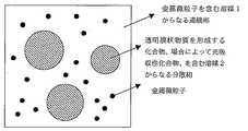
本発明の塗布液は、溶媒1に金属微粒子が分散した金属微粒子分散液と、かかる溶媒1に難溶な溶媒2を用いて上記の透明膜状物質を形成可能な化合物を溶解させた化合物溶液、場合によりかかる化合物溶液に光吸収性化合物等の添加剤を溶解及び/又は分散させた化合物溶液を、必要に応じて界面活性剤の存在のもと混合して得られるエマルションである。なお、溶媒1及び溶媒2は、夫々、単独の溶媒であっても混合溶媒であっても良い。かかるエマルションにおいて、該金属微粒子分散液は連続相を形成し、一方、該化合物溶液は分散相(不連続相)を形成する(図1参照)。溶媒1が水を主体とした溶媒である場合、溶媒2はかかる溶媒に難溶な溶媒から構成され、かかるエマルションは、O/W(oil in water)エマルションとなる。一方、溶媒2が水を主体とした溶媒である場合、溶媒1はかかる溶媒に難溶な溶媒から構成され、かかるエマルションは、W/O(water in oil)エマルションとなる。なお、首記の難溶とは、必要に応じて適切な界面活性剤の選択により、エマルションを形成できる溶媒の組み合わせを指す。The substrate with a transparent conductive film of the present invention is produced by applying a coating solution described below on the transparent substrate.
The coating liquid of the present invention is a compound solution obtained by dissolving a compound capable of forming a transparent film-like substance using a metal fine particle dispersion in which metal fine particles are dispersed in a solvent 1 and a solvent 2 that is hardly soluble in the solvent 1. An emulsion obtained by optionally mixing a compound solution in which an additive such as a light-absorbing compound is dissolved and / or dispersed in such a compound solution in the presence of a surfactant as required. Each of the solvent 1 and the solvent 2 may be a single solvent or a mixed solvent. In such an emulsion, the metal fine particle dispersion forms a continuous phase, while the compound solution forms a dispersed phase (discontinuous phase) (see FIG. 1). When the solvent 1 is a solvent mainly composed of water, the solvent 2 is composed of a solvent that is hardly soluble in the solvent, and the emulsion is an O / W (oil in water) emulsion. On the other hand, when the solvent 2 is a solvent mainly composed of water, the solvent 1 is composed of a solvent that is hardly soluble in the solvent, and the emulsion is a W / O (water in oil) emulsion. In addition, the hardly soluble mentioned above refers to a combination of solvents that can form an emulsion by selecting an appropriate surfactant as required.
O/Wエマルション、W/Oエマルションの選択は任意であり、塗布液の主要成分である該透明膜状物質を形成する化合物の溶解性、場合により該光吸収性化合物等の添加剤の溶解性及び/又は分散性、及び該金属微粒子の分散性を考慮して適宜選択される。
本発明の塗布液を構成する該金属微粒子分散液における該金属微粒子は、本発明の透明導電膜付き基板において導電性を提供する金属網目を形成するためのものであり、金属網目を形成する金属として前述の金属が挙げられる。これらの金属微粒子は、還元法、気相法、粉砕法等の公知の方法により製造される。The selection of O / W emulsion and W / O emulsion is arbitrary, the solubility of the compound that forms the transparent film-like substance that is the main component of the coating liquid, and optionally the solubility of additives such as the light-absorbing compound And / or appropriately selected in consideration of dispersibility and dispersibility of the metal fine particles.
The metal fine particles in the metal fine particle dispersion constituting the coating liquid of the present invention are for forming a metal network providing conductivity in the substrate with a transparent conductive film of the present invention. As mentioned above. These metal fine particles are produced by a known method such as a reduction method, a gas phase method, or a pulverization method.
該金属微粒子の平均粒径(直径)は、0.005μm〜1μm、好ましくは0.01μm〜0.5μ
m、より好ましくは0.01μm〜0.2μmの範囲である。かかる範囲より小さなものは、接
触抵抗が増大し良好な導電性が得られない傾向がある。一方、かかる範囲よりも大きなものは分散不良を起こしやすくなり、また、良好な導電性が得られない傾向がある。なお、金属微粒子の形状は、球状、鱗片状、針状、樹枝状、鎖状など任意の形状のものを用いることができる。また用いる金属微粒子の粒径が、大きい粒子と小さい粒子との混合系であっても構わない。また導電性を向上させる目的で、添加剤として、金属塩化合物、金属錯体化合物、金属酸化物等を加えてもよい。The average particle diameter (diameter) of the metal fine particles is 0.005 μm to 1 μm, preferably 0.01 μm to 0.5 μm.
m, more preferably in the range of 0.01 μm to 0.2 μm. If it is smaller than this range, the contact resistance increases and good conductivity tends not to be obtained. On the other hand, those larger than this range tend to cause poor dispersion, and there is a tendency that good conductivity cannot be obtained. The shape of the metal fine particles may be any shape such as a spherical shape, a scale shape, a needle shape, a dendritic shape, or a chain shape. The metal fine particles used may be a mixed system of large particles and small particles. Further, for the purpose of improving conductivity, a metal salt compound, a metal complex compound, a metal oxide, or the like may be added as an additive.
該金属微粒子分散液に含有される金属粒子の濃度は、該金属微粒子分散液中の重量濃度として、0.1〜80重量%、好ましくは1〜50重量%、より好ましくは3〜30重量%の範囲で
ある。かかる範囲の下限よりも少なくなると、導電性が低下する傾向にあるため好ましくない。一方、かかる範囲の上限よりも多くなると、得られる金属網目構造の開口部面積が減少し、透明性が低下する傾向にあり、また、塗布液の安定性が低下するため好ましくない。The concentration of the metal particles contained in the metal fine particle dispersion is in the range of 0.1 to 80% by weight, preferably 1 to 50% by weight, more preferably 3 to 30% by weight as the weight concentration in the metal fine particle dispersion. It is. If the amount is less than the lower limit of the range, the conductivity tends to decrease, such being undesirable. On the other hand, if the amount exceeds the upper limit of the range, the opening area of the obtained metal network structure tends to be reduced, the transparency tends to be lowered, and the stability of the coating solution is lowered.
該金属微粒子分散液には、更に、金属微粒子の分散安定性を高めるための添加剤や得られる金属網目の強度や透明基板との接着性を更に高めるための樹脂成分を適宜添加してもよい。このような添加成分の例としては、溶媒1が水系の場合、クエン酸等の多価カルボン酸類、ポリビニルアルコール系樹脂、ポリ(メタ)アクリル酸系樹脂、ポリビニルブチラール系樹脂、ポリビニルピロリドン系樹脂、ポリエチレングリコール系樹脂、セルロース系樹脂等が例示され、これらは単独でも、または混合して用いてもよい。一方、溶媒1が水と実質的に非混和な溶媒の場合、ポリビニルブチラール系樹脂、フェノキシ系樹脂、ポリウレタン系樹脂、ポリメチルメタクリレート樹脂等のアクリレート系樹脂、ポリカーボ
ネート樹脂、ポリスチレン系樹脂、エチレン−酢酸ビニル共重合体樹脂、AS樹脂、塩酢ビ樹脂などが挙げられる。これらは単独でも、または混合して用いてもよい。The metal fine particle dispersion may further be appropriately added with an additive for enhancing the dispersion stability of the metal fine particles and a resin component for further enhancing the strength of the resulting metal network and the adhesion to the transparent substrate. . Examples of such additive components include, when the solvent 1 is aqueous, polyvalent carboxylic acids such as citric acid, polyvinyl alcohol resins, poly (meth) acrylic resins, polyvinyl butyral resins, polyvinyl pyrrolidone resins, Examples thereof include polyethylene glycol resins and cellulose resins, which may be used alone or in combination. On the other hand, when the solvent 1 is a solvent substantially immiscible with water, polyvinyl butyral resin, phenoxy resin, polyurethane resin, acrylate resin such as polymethyl methacrylate resin, polycarbonate resin, polystyrene resin, ethylene-acetic acid Examples include vinyl copolymer resins, AS resins, and vinyl acetate resins. These may be used alone or in combination.
通常、該金属微粒子分散液中の添加剤の濃度は、該金属微粒子分散液中の重量濃度として、30重量%以下が好ましい。これを越えると、導電性が悪化するため好ましくない。
該金属微粒子分散液は、必要に応じて分散処理して製造される。かかる分散処理に使用する分散機としては、これに限定されるものではないが、ボールミル、サンドミル、コロイドミル、アトライター、パールミル、コボールミル、ホモミキサー、ホモジナイザー、マグネティックスターラー、ペイントシェーカー、超音波ホモジナイザー等の公知の方法を用いることができる。分散機としてメディアを使うものには、例えば、ガラスビーズ、ジルコニアビーズ、アルミナビーズ等を用いることができる。
なお、該金属微粒子分散液には、本発明の効果を損なわない範囲において、通常、微粒子分散液に添加される各種添加剤、例えば、酸化防止剤、表面張力調整剤、粘度調整剤、pH調整剤、防腐剤、キレート剤、消泡剤等が必要に応じて含まれていても良い。Usually, the concentration of the additive in the fine metal particle dispersion is preferably 30% by weight or less as the weight concentration in the fine metal particle dispersion. Exceeding this is not preferable because the conductivity deteriorates.
The metal fine particle dispersion is produced by a dispersion treatment as necessary. Dispersers used for such dispersion processing are not limited to these, but include ball mills, sand mills, colloid mills, attritors, pearl mills, coball mills, homomixers, homogenizers, magnetic stirrers, paint shakers, ultrasonic homogenizers, etc. These known methods can be used. For example, glass beads, zirconia beads, alumina beads, or the like can be used as the dispersing machine.
In addition, in the metal fine particle dispersion, various additives usually added to the fine particle dispersion, for example, an antioxidant, a surface tension adjuster, a viscosity adjuster, a pH adjuster, as long as the effects of the present invention are not impaired. Agents, preservatives, chelating agents, antifoaming agents and the like may be included as necessary.
本発明の塗布液を構成する化合物溶液に含まれる透明膜状物質を形成する化合物は、本発明の透明導電膜付き基板において金属網目と透明基板との密着性および/または金属網目の強度を向上させるものである。該透明膜状物質を形成する化合物は、前述のとおりであるが、さらに塗布後に重合させる場合であれば、熱硬化性樹脂モノマーや紫外線硬化樹脂モノマー等、公知のモノマーから適宜選択して使用することができる。該透明膜状物質を形成する化合物の濃度は、該化合物溶液中の重量濃度として、0.01重量%〜50重量%の範囲が好ましい。0.01重量%を下回ると、得られる金属網目と透明基板との密着性向上および/または金属網目の強度向上が不十分となる傾向がある。一方、50重量%を越えると、化合物溶液の粘度が上昇したり、透明導電膜が形成不良を起こす怖れがある。 The compound forming the transparent film-like substance contained in the compound solution constituting the coating solution of the present invention improves the adhesion between the metal network and the transparent substrate and / or the strength of the metal network in the substrate with a transparent conductive film of the present invention. It is something to be made. The compound that forms the transparent film-like substance is as described above, and if it is further polymerized after coating, it is appropriately selected from known monomers such as thermosetting resin monomers and ultraviolet curable resin monomers. be able to. The concentration of the compound forming the transparent film-like substance is preferably in the range of 0.01% by weight to 50% by weight as the weight concentration in the compound solution. When it is less than 0.01% by weight, the adhesion between the resulting metal network and the transparent substrate and / or the strength of the metal network tend to be insufficient. On the other hand, if it exceeds 50% by weight, the viscosity of the compound solution may increase or the transparent conductive film may be poorly formed.
該化合物溶液に光吸収性化合物を含有する場合の濃度は、該光吸収性化合物の吸光度及び透明導電膜付き基板に要求される特定波長の光の吸収性によって定まるため、一概にその値を規定することはできないが、通常、該化合物溶液中の重量濃度として、0.0001重量%〜50重量%の範囲が好ましい。0.0001重量%を下回ると、得られる透明導電膜付き基板の特定の光吸収性が十分に発現しないこととなる。一方、50重量%を越えると、該光吸収性化合物の溶解不良や分散不良が起き易くなる傾向にある。 The concentration when the compound solution contains a light-absorbing compound is determined by the absorbance of the light-absorbing compound and the light-absorbing property of the specific wavelength required for the substrate with a transparent conductive film. Usually, the weight concentration in the compound solution is preferably in the range of 0.0001% to 50% by weight. If it is less than 0.0001% by weight, the specific light-absorbing property of the obtained substrate with a transparent conductive film is not sufficiently exhibited. On the other hand, if it exceeds 50% by weight, poor dissolution or dispersion of the light absorbing compound tends to occur.
該化合物溶液における該光吸収性化合物は、上記溶媒2中において、分子状に溶解していても良く、また、会合体を形成して溶解していても良い。更に、粒子状に分散している状態でもよい。かかる粒子状に分散する場合には、透明導電膜付き基板を作製した際に、該粒子に起因する可視光散乱による濁りが発生しやすくなるため、これを抑制するために、通常、0.5μm以下、好ましくは0.3μm以下、より好ましくは0.15μm以下の粒径に分散することが望ましい。 The light-absorbing compound in the compound solution may be dissolved in a molecular form in the solvent 2 or may be dissolved by forming an aggregate. Further, it may be dispersed in the form of particles. When dispersed in such a particle form, when a substrate with a transparent conductive film is produced, turbidity due to visible light scattering due to the particles is likely to occur, and in order to suppress this, usually 0.5 μm or less It is desirable to disperse to a particle size of preferably 0.3 μm or less, more preferably 0.15 μm or less.
該化合物溶液の調製方法は、公知の方法をもってなされ、特に限定されるものではないが、マグネティックスターラーや、通常の羽翼を備えた撹拌機による撹拌の他、高速の分散機、超音波分散機、ホモジナイザー等でおこなうことができる。また、該光吸収性化合物を該化合物溶液に分散する場合は、適宜、公知の分散剤を併用し、公知の分散処理、例えば、ボールミル、サンドミル、コロイドミル、アトライター、パールミル、コボールミル、ホモミキサー、ホモジナイザー、マグネティックスターラー、ペイントシェーカー、超音波ホモジナイザー等の方法を用いて調製することができる。分散機としてメディアを使うものには、例えば、ガラスビーズ、ジルコニアビーズ、アルミナビーズ等を用いることができる。 The method for preparing the compound solution is a known method, and is not particularly limited. In addition to stirring with a magnetic stirrer or a stirrer equipped with a normal blade, a high-speed disperser, an ultrasonic disperser, This can be done with a homogenizer. In addition, when the light absorbing compound is dispersed in the compound solution, a known dispersing agent is appropriately used in combination with a known dispersing treatment such as a ball mill, a sand mill, a colloid mill, an attritor, a pearl mill, a coball mill, a homomixer. It can be prepared by using a method such as a homogenizer, a magnetic stirrer, a paint shaker, or an ultrasonic homogenizer. For example, glass beads, zirconia beads, alumina beads, or the like can be used as the dispersing machine.
なお、該化合物溶液には、本発明の効果を損なわない範囲において、各種添加剤、例え
ば、酸化防止剤、表面張力調整剤、粘度調製剤、pH調整剤、防腐剤、キレート剤、消泡剤等が必要に応じて含まれていても良い。
本発明の塗布液は、上記の金属微粒子分散液と化合物溶液を界面活性剤の存在のもと機械的に混合して得られるエマルションである。かかる化合物溶液に含まれる該透明膜状物質を形成する化合物が水もしくは水を主体とした溶媒に溶解する場合、さらに場合によっては、かかる化合物溶液に含まれても良い該光吸収性化合物が水もしくは水を主体とした溶媒に溶解及び/もしくは分散する場合、溶媒2として水もしくは水を主体とした溶媒を用いた該化合物溶液が、適切な界面活性剤の選択のもと分散相をなすW/Oエマルションを
なすように、金属微粒子分散液の溶媒1を選択する。溶媒2として水もしくは水を主体とした溶媒を用いた場合、溶媒1は、金属微粒子の分散性に応じて選択されることが好ましい。一方、かかる化合物溶液に含まれる該透明膜状物質を形成する化合物が水に難溶な溶媒に溶解する場合、さらに場合によっては、かかる化合物溶液に含まれても良い該光吸収性化合物が、水に難溶な溶媒に溶解及び/もしくは分散する場合、溶媒2としてかかる溶媒を用いた該化合物溶液が、適切な界面活性剤の選択のもと分散相をなすO/Wエマルショ
ンをなすように、金属微粒子分散液の溶媒1を水もしくは水を主体とした溶媒とする。溶媒1として水もしくは水を主体とした溶媒を用いた場合、溶媒2としては、該透明膜状物質を形成する化合物の溶解性、さらに場合によっては光吸収性化合物の溶解性及び/又は分散性に応じて選択されることが好ましい。In the compound solution, various additives such as an antioxidant, a surface tension adjusting agent, a viscosity adjusting agent, a pH adjusting agent, a preservative, a chelating agent, and an antifoaming agent are added within a range not impairing the effects of the present invention. Etc. may be included as necessary.
The coating liquid of the present invention is an emulsion obtained by mechanically mixing the metal fine particle dispersion and the compound solution in the presence of a surfactant. When the compound that forms the transparent film-like substance contained in the compound solution is dissolved in water or a solvent mainly composed of water, the light-absorbing compound that may be contained in the compound solution may be water. Alternatively, when dissolved and / or dispersed in a water-based solvent, the compound solution using water or a water-based solvent as the solvent 2 forms a dispersed phase under the selection of an appropriate surfactant. The solvent 1 of the metal fine particle dispersion is selected so as to form an / O emulsion. When water or a solvent mainly composed of water is used as the solvent 2, the solvent 1 is preferably selected according to the dispersibility of the metal fine particles. On the other hand, when the compound that forms the transparent film-like substance contained in the compound solution is dissolved in a solvent that is hardly soluble in water, the light absorbing compound that may be contained in the compound solution may be When dissolved and / or dispersed in a water-insoluble solvent, the compound solution using such a solvent as solvent 2 forms an O / W emulsion that forms a dispersed phase under the selection of an appropriate surfactant. The solvent 1 of the metal fine particle dispersion is water or a solvent mainly composed of water. When water 1 or a solvent mainly composed of water is used as the solvent 1, the solvent 2 is soluble in the compound that forms the transparent film-like substance, and in some cases, is soluble and / or dispersible in the light-absorbing compound. It is preferable to select according to.
かかる溶媒の組み合わせとしては、金属微粒子の分散性、透明膜状物質を形成する化合物の溶解性、及び場合により含有される光吸収性化合物の溶解性及び/又は分散性に応じて選択されるため、特に限定されるわけではないが、溶媒1(あるいは溶媒2)を水もしくは水を主体とした溶媒とした場合、溶媒2(あるいは溶媒1)としては、例えば、トルエン、キシレン、エチルベンゼン、トリメチルベンゼン、メチルシクロヘキサン、メチルシクロペンタン、ヘキサン、ヘプタン、オクタン、デカン、石油エーテル、石油ベンジン、テレピン油等で例示される炭化水素系溶媒、クロロホルム、1,1−ジクロロエタン、1,2−ジクロロエタン、トリクロロエチレン、1,1,2−トリクロロエタン等で例示されるハロゲン系溶媒、エチル−n−ブチルケトン、ジイソブチルケトン、ジイソプロピルケトン、シクロペンタノン、シクロヘキサノン、ジ−n−プロピルケトン、メチルイソブチルケトン、メチルエチルケトン、メチルシクロヘキサノン、メチル−n−ブチルケトン、メチル−n−プロピルケトン、イソホロン等で例示されるケトン系溶媒、安息香酸エチル、安息香酸ブチル、酢酸エチル、酢酸−n−ブチル、酢酸イソブチル、酢酸シクロヘキシル、酢酸sブチル、酢酸ベンジル、酢酸メチルシクロヘキシル等で例示されるエステ
ル系溶媒などが例示される。なお、これらの溶媒は単独で用いても、あるいは2種以上混合して用いても良い。Such a solvent combination is selected according to the dispersibility of the metal fine particles, the solubility of the compound forming the transparent film-like substance, and the solubility and / or dispersibility of the light-absorbing compound contained in some cases. Although not particularly limited, when the solvent 1 (or solvent 2) is water or a solvent mainly composed of water, examples of the solvent 2 (or solvent 1) include toluene, xylene, ethylbenzene, and trimethylbenzene. , Hydrocarbon solvents exemplified by methylcyclohexane, methylcyclopentane, hexane, heptane, octane, decane, petroleum ether, petroleum benzine, turpentine oil, chloroform, 1,1-dichloroethane, 1,2-dichloroethane, trichloroethylene, A halogenated solvent exemplified by 1,1,2-trichloroethane and the like, ethyl Examples include n-butyl ketone, diisobutyl ketone, diisopropyl ketone, cyclopentanone, cyclohexanone, di-n-propyl ketone, methyl isobutyl ketone, methyl ethyl ketone, methyl cyclohexanone, methyl-n-butyl ketone, methyl-n-propyl ketone, isophorone, etc. Ketone solvents, ethyl benzoate, butyl benzoate, ethyl acetate, n-butyl acetate, isobutyl acetate, cyclohexyl acetate, sbutyl acetate, benzyl acetate, methyl cyclohexyl acetate, and the like. The These solvents may be used alone or in combination of two or more.
なお、光吸収性化合物は、通常、水に対する溶解性が低いことから、水に難溶な溶媒に溶解させた化合物溶液を用い、連続相として水系の金属微粒子分散液を用いるO/Wエマル
ションか、もしくは、水に光吸収性化合物を分散させた化合物溶液を用い、水に難溶な溶媒を用いた金属微粒子分散液を用いるW/Oエマルションが好ましい。あるいは、光吸収性
化合物に化学修飾を施し、水に対する溶解性を高めることによって、W/Oエマルションと
することもできる。The light-absorbing compound usually has a low solubility in water, so a compound solution dissolved in a solvent that is hardly soluble in water is used, and an O / W emulsion using an aqueous metal fine particle dispersion as a continuous phase. Alternatively, a W / O emulsion using a compound solution in which a light-absorbing compound is dispersed in water and a metal fine particle dispersion using a solvent that is hardly soluble in water is preferable. Or it can also be set as a W / O emulsion by chemically modifying a light absorptive compound and improving the solubility with respect to water.
エマルションにおいて連続相をなす金属微粒子分散液Cと分散相をなす化合物溶液Dの比率は、重量にてD/C=1/20〜20/1である。本発明の網目構造を良好に形成させるためには、D/C=1/15〜10/1が好ましく、より好ましくは1/10〜5/1、とりわけ1/5〜3/1の範囲が好適である。分散相の比率がかかる上限を越えると、エマルションの形成に難があり、また、エマルションの分散性が悪化する傾向にある。一方、分散相の比率が下限を下回ると、得られる透明導電膜付き基板の透明性が悪化する傾向にある。 The ratio of the metal fine particle dispersion C forming the continuous phase to the compound solution D forming the dispersion phase in the emulsion is D / C = 1/20 to 20/1 by weight. In order to satisfactorily form the network structure of the present invention, D / C = 1/15 to 10/1 is preferable, more preferably 1/10 to 5/1, especially 1/5 to 3/1. Is preferred. When the ratio of the dispersed phase exceeds the upper limit, it is difficult to form an emulsion, and the dispersibility of the emulsion tends to deteriorate. On the other hand, when the ratio of the dispersed phase is below the lower limit, the transparency of the obtained substrate with a transparent conductive film tends to deteriorate.
かかるエマルションを形成するための界面活性剤としては、特に限定されるものではなく、公知のアニオン性界面活性剤、カチオン性界面活性剤、ノニオン性界面活性剤、両性界面活性剤等の各種界面活性剤を用いることができる。
そのアニオン性界面活性剤としては、具体的には、例えば、ラウリン酸ナトリウム、ステアリン酸ナトリウム、オレイン酸ナトリウム等の高級脂肪酸塩類、ドデシル硫酸ナトリウム、ラウリル硫酸ナトリウム、セチル硫酸ナトリウム、ステアリル硫酸ナトリウム、オレイル硫酸ナトリウム等のアルキル硫酸エステル塩類、オクチルアルコール硫酸エステルナトリウム、ラウリルアルコール硫酸エステルナトリウム、ラウリルアルコール硫酸エステルアンモニウム等の高級アルコール硫酸エステル塩類、アセチルアルコール硫酸エステルナトリウム等の脂肪族アルコール硫酸エステル塩類、ラウリルベンゼンスルホン酸ナトリウム、セチルベンゼンスルホン酸ナトリウム、ステアリルベンゼンスルホン酸ナトリウム、オレイルベンゼンスルホン酸ナトリウム等のアルキルベンゼンスルホン酸塩類、イソプロピルナフタレンスルホン酸ナトリウム等のアルキルナフタレンスルホン酸塩類、アルキルジフェニルエーテルジスルホン酸ナトリウム等のアルキルジフェニルエーテルジスルホン酸塩類、ラウリル燐酸ナトリウム、ステアリル燐酸ナトリウム等のアルキル燐酸エステル塩類、ラウリルエーテル硫酸ナトリウムのポリエチレンオキサイド付加物、ラウリルエーテル硫酸アンモニウムのポリエチレンオキサイド付加物、ラウリルエーテル硫酸トリエタノールアミンのポリエチレンオキサイド付加物等のアルキルエーテル硫酸塩のポリエチレンオキサイド付加物類、ノニルフェニルエーテル硫酸ナトリウムのポリエチレンオキサイド付加物等のアルキルフェニルエーテル硫酸塩のポリエチレンオキサイド付加物類、ラウリルエーテル燐酸ナトリウムのポリエチレンオキサイド付加物等のアルキルエーテル燐酸塩のポリエチレンオキサイド付加物類、ノニルフェニルエーテル燐酸ナトリウムのポリエチレンオキサイド付加物等のアルキルフェニルエーテル燐酸塩のポリエチレンオキサイド付加物類等を挙げることができる。The surfactant for forming such an emulsion is not particularly limited, and various surfactants such as known anionic surfactants, cationic surfactants, nonionic surfactants, and amphoteric surfactants. An agent can be used.
Specific examples of the anionic surfactant include higher fatty acid salts such as sodium laurate, sodium stearate, and sodium oleate, sodium dodecyl sulfate, sodium lauryl sulfate, sodium cetyl sulfate, sodium stearyl sulfate, and oleyl. Alkyl sulfates such as sodium sulfate, higher alcohol sulfates such as sodium octyl alcohol sulfate, sodium lauryl alcohol sulfate, ammonium lauryl alcohol sulfate, aliphatic alcohol sulfates such as sodium acetyl alcohol sulfate, lauryl benzene Sodium sulfonate, sodium cetylbenzenesulfonate, sodium stearylbenzenesulfonate, oleylbenzenesulfone Alkylbenzenesulfonates such as sodium, alkylnaphthalenesulfonates such as sodium isopropylnaphthalenesulfonate, alkyldiphenylether disulfonates such as sodium alkyldiphenyletherdisulfonate, alkylphosphate esters such as sodium lauryl phosphate and sodium stearylphosphate, lauryl ether Polyethylene oxide adducts of alkyl ether sulfate such as polyethylene oxide adduct of sodium sulfate, polyethylene oxide adduct of lauryl ether ammonium sulfate, polyethylene oxide adduct of lauryl ether sulfate triethanolamine, polyethylene oxide addition of sodium nonylphenyl ether sulfate Of alkyl phenyl ether sulfates Polyethylene oxide adducts of alkyl ether phosphates such as polyethylene oxide adducts such as lenoxide oxide adducts, polyethylene oxide adducts of sodium lauryl ether phosphate, polyethylene oxide adducts of alkyl phenyl ether phosphates such as polyethylene oxide adducts of sodium nonylphenyl ether phosphate And the like.
又、カチオン性界面活性剤としては、具体的には、例えば、ラウリルトリメチルアンモニウムクロライド、セチルトリメチルアンモニウムクロライド、セチルトリメチルアンモニウムブロマイド、ステアリルトリメチルアンモニウムクロライド、ベヘニルトリメチルアンモニウムクロライド、ジステアリルジメチルアンモニウムクロライド、ラノリン誘導第4級アンモニウム塩等の第4級アンモニウム塩類、ラウリルピリジニウムクロライド、ラウリルピリジニウムブロマイド、セチルピリジニウムクロライド等のピリジニウム塩類、2−ステアリル−ヒドロキシエチル−2−イミダゾリン誘導体等のイミダゾリニウム塩類、N,N−ジエチル−ステアロアミド−メチルアミン塩酸塩、ポリオキシエチレンステアリルアミン等のアミン塩類等を挙げることができる。 Specific examples of the cationic surfactant include lauryltrimethylammonium chloride, cetyltrimethylammonium chloride, cetyltrimethylammonium bromide, stearyltrimethylammonium chloride, behenyltrimethylammonium chloride, distearyldimethylammonium chloride, lanolin derivative. Quaternary ammonium salts such as quaternary ammonium salts, pyridinium salts such as lauryl pyridinium chloride, lauryl pyridinium bromide, cetyl pyridinium chloride, imidazolinium salts such as 2-stearyl-hydroxyethyl-2-imidazoline derivatives, N, N -Amine salts such as diethyl-stearamide-methylamine hydrochloride, polyoxyethylene stearylamine, etc. It can be mentioned.
又、ノニオン性界面活性剤としては、具体的には、例えば、ポリエチレングリコールセチルエーテル、ポリエチレングリコールステアリルエーテル、ポリエチレングリコールオレイルエーテル、ポリエチレングリコールベヘニルエーテル等のポリエチレングリコールアルキルエーテル類、ポリエチレングリコールポリプロピレングリコールセチルエーテル、ポリエチレングリコールポリプロピレングリコールデシルテトラデシルエーテル等のポリエチレングリコールポリプロピレングリコールアルキルエーテル類、ポリエチレングリコールオクチルフェニルエーテル、ポリエチレングリコールノニルフェニルエーテル等のポリエチレングリコールアルキルフェニルエーテル類、モノステアリン酸エチレングリコール、ジステアリン酸エチレングリコール、ステアリン酸ジエチレングリコール、ジステアリン酸ポリエチレングリコール、モノラウリン酸ポリエチレングリコール、モノステアリン酸ポリエチレングリコール、モノオレイン酸ポリエチレングリコール等のポリエチレングリコール脂肪酸エステル類、モノミリスチン酸グリセリル、モノステアリン酸グリセリル、モノイソステアリン酸グリセリル、ジステアリン酸グリセリル、ジオレイン酸グリセリル等のグリセリン脂肪酸エステル類、モノパルミチン酸ソルビタン、モノステアリン
酸ソルビタン、トリステアリン酸ソルビタン、モノオレイン酸ソルビタン、トリオレイン酸ソルビタン等のソルビタン脂肪酸エステル類、モノステアリン酸グリセリルのポリエチレンオキサイド付加物、モノオレイン酸グリセリルのポリエチレンオキサイド付加物等のグリセリン脂肪酸エステルのポリエチレンオキサイド付加物類、モノパルミチン酸ソルビタンのポリエチレンオキサイド付加物、モノステアリン酸ソルビタンのポリエチレンオキサイド付加物、トリステアリン酸ソルビタンのポリエチレンオキサイド付加物、モノオレイン酸ソルビタンのポリエチレンオキサイド付加物、トリオレイン酸ソルビタンのポリエチレンオキサイド付加物等のソルビタン脂肪酸エステルのポリエチレンオキサイド付加物類、モノラウリン酸ソルビットのポリエチレンオキサイド付加物、テトラステアリン酸ソルビットのポリエチレンオキサイド付加物、ヘキサステアリン酸ソルビットのポリエチレンオキサイド付加物、テトラオレイン酸ソルビットのポリエチレンオキサイド付加物等のソルビット脂肪酸エステルのポリエチレンオキサイド付加物類、ヒマシ油のポリエチレンオキサイド付加物類等を挙げることができる。Specific examples of nonionic surfactants include polyethylene glycol alkyl ethers such as polyethylene glycol cetyl ether, polyethylene glycol stearyl ether, polyethylene glycol oleyl ether, polyethylene glycol behenyl ether, and polyethylene glycol polypropylene glycol cetyl ether. Polyethylene glycol polypropylene glycol alkyl ethers such as polyethylene glycol polypropylene glycol decyl tetradecyl ether, polyethylene glycol alkyl phenyl ethers such as polyethylene glycol octyl phenyl ether and polyethylene glycol nonyl phenyl ether, ethylene glycol monostearate, ethylene distearate Recall, diethylene glycol stearate, polyethylene glycol distearate, polyethylene glycol monolaurate, polyethylene glycol monostearate, polyethylene glycol monooleate, glyceryl monomyristate, glyceryl monostearate, glyceryl monoisostearate, Glycerin fatty acid esters such as glyceryl distearate and glyceryl dioleate, sorbitan monopalmitate, sorbitan monostearate, sorbitan tristearate, sorbitan monooleate, sorbitan trioleate, glyceryl monostearate Polyethylene oxide adduct, glyceryl monooleate Polyethylene oxide adducts of glycerin fatty acid esters such as lenoxide adducts, polyethylene oxide adducts of sorbitan monopalmitate, polyethylene oxide adducts of sorbitan monostearate, polyethylene oxide adducts of sorbitan tristearate, sorbitan monooleate Polyethylene oxide adducts, polyethylene oxide adducts of sorbitan fatty acid esters such as polyethylene oxide adduct of sorbitan trioleate, polyethylene oxide adduct of sorbitol monolaurate, polyethylene oxide adduct of sorbitol tetrastearate, sorbitol hexastearate Polyethylene oxide adducts such as polyethylene oxide adducts of sorbite tetraoleate Examples thereof include polyethylene oxide adducts of rubbit fatty acid esters and polyethylene oxide adducts of castor oil.
また、両性界面活性剤としては、例えば、2−ウンデシル−N,N,N−(ヒドロキシエチルカルボキシルメチル)−2−イミダゾリンナトリウム等のイミダゾリン系両性界面活性剤、ラウリルジメチルアミノ酢酸ベタイン、アルキルベタイン、スルホベタイン、アミドベタイン、等のベタイン系界面活性剤等を挙げることができる。
また、界面活性能を有する樹脂成分を添加しても良く、例えば、ポリビニルアルコール、(メタ)アクリル酸/(メタ)アルキルアクリレート共重合体、(メタ)アクリル酸/スチレン共重合体等の親水性モノマー及び疎水性モノマー共重合体、ヒドロキシプロピルセルロース、ヒドロキシプロピルメチルセルロース、ヒドロキシエチルセルロース、カルボキシメチルセルロース等のセルロース系樹脂、ポリエチレングリコール及びポリプロピレングリコールからなるブロック共重合体等が挙げられる。Examples of the amphoteric surfactant include imidazoline-based amphoteric surfactants such as 2-undecyl-N, N, N- (hydroxyethylcarboxylmethyl) -2-imidazoline sodium, lauryldimethylaminoacetic acid betaine, alkylbetaine, Examples include betaine surfactants such as sulfobetaine and amide betaine.
In addition, a resin component having surface activity may be added. For example, hydrophilic properties such as polyvinyl alcohol, (meth) acrylic acid / (meth) alkyl acrylate copolymer, (meth) acrylic acid / styrene copolymer, etc. Examples thereof include monomers and hydrophobic monomer copolymers, cellulose resins such as hydroxypropylcellulose, hydroxypropylmethylcellulose, hydroxyethylcellulose, and carboxymethylcellulose, and block copolymers composed of polyethylene glycol and polypropylene glycol.
これらの界面活性剤は、1種又は2種以上組み合わせて用いることができ、例えば、HLBの低いものと高いものを2種以上組み合わせて安定したエマルションとすることができる。
界面活性剤の添加量は、金属微粒子分散液及び化合物溶液を合わせた液重量に対し、0 〜 20重量%、好ましくは0.001 〜 10重量%、より好ましくは0.01 〜 5重量%である。
添加量が下限を下回るとエマルションが形成されなかったり、安定なエマルションが得られないため好ましくないが、該金属微粒子分散液および該化合物溶液のみでエマルションが得られる場合は、必ずしも界面活性剤を添加しなくてもよい。また、添加量が上限を上回ると、得られる金属網目の導電性の悪化、塗布膜強度の低下等の悪影響があるため好ましくない。These surfactants can be used singly or in combination of two or more. For example, two or more kinds of low and high HLB can be combined to form a stable emulsion.
The addition amount of the surfactant is 0 to 20% by weight, preferably 0.001 to 10% by weight, more preferably 0.01 to 5% by weight, based on the combined weight of the metal fine particle dispersion and the compound solution.
If the amount added is less than the lower limit, an emulsion is not formed or a stable emulsion cannot be obtained, which is not preferable. However, when an emulsion can be obtained only with the metal fine particle dispersion and the compound solution, a surfactant is not necessarily added. You don't have to. Moreover, when the addition amount exceeds the upper limit, it is not preferable because there are adverse effects such as deterioration of conductivity of the obtained metal network and reduction of coating film strength.
本発明のエマルションは、以上の金属微粒子分散液ならびに化合物溶液を混合し、公知の乳化方法によって調製することができる。この際、上記の界面活性剤は、適宜、金属微粒子分散液もしくは/及び化合物溶液に添加される。乳化の方法は特に限定されることはないが、例えば、羽翼を備えた撹拌機による撹拌、ホモミキサー、オムニミキサー、バブルホモジナイザー、ピストンホモジナイザー、超音波乳化器、マイクロ流動化装置(例えば、マイクロフルーディックス社製「マイクロフルーダイザー」)等の剪断混合装置によって均一に混合し、乳化される。 The emulsion of the present invention can be prepared by a known emulsification method by mixing the above metal fine particle dispersion and the compound solution. At this time, the above surfactant is appropriately added to the metal fine particle dispersion or / and the compound solution. The emulsification method is not particularly limited. For example, stirring with a stirrer equipped with a blade, homomixer, omni mixer, bubble homogenizer, piston homogenizer, ultrasonic emulsifier, microfluidizer (for example, microfluidizer). The mixture is uniformly mixed and emulsified by a shear mixing device such as “Microfluidizer” manufactured by Dix.
本発明の透明導電膜付き基板は、透明基板上に上記塗布液を塗布し、乾燥を経るものであれば限定はなく、公知の塗布方法、例えば、ディッピング法、スピンコート法、ワイヤーバーコート法、スプレー法、ロールコーター法などを用いることができる。なお、塗布液が塗布される透明基板と塗布液との濡れ性が不良な場合には、かかる濡れ性を向上させるために、本発明の効果を損なわない範囲において、透明基板の表面を処理することが好ましい。かかる表面処理については、公知の方法を選択すれば良く、例えば、コロナ放電
処理、火炎処理、プラズマ処理、グロー放電処理、粗面化処理、薬品処理等の方法による表面処理や、アンカーコート剤やプライマー等のコーティングを施し、表面の疎水性、親水性の度合いを調節しても良い。また、本発明の効果を損なわない範囲において、塗布液への粘度調製剤の添加を併用してもよい。
かかる塗布、乾燥された透明導電膜付き基板に対し、導電性を向上させる目的で別途熱処理を施してもよい。熱処理温度は、透明基板の耐熱温度以下であれば特に限定されない。The substrate with a transparent conductive film of the present invention is not limited as long as the coating liquid is applied onto the transparent substrate and dried, and known coating methods such as dipping, spin coating, and wire bar coating are applicable. A spray method, a roll coater method, or the like can be used. In addition, when the wettability between the transparent substrate to which the coating liquid is applied and the coating liquid is poor, the surface of the transparent substrate is treated within a range that does not impair the effects of the present invention in order to improve the wettability. It is preferable. For such surface treatment, a known method may be selected. For example, surface treatment by a method such as corona discharge treatment, flame treatment, plasma treatment, glow discharge treatment, roughening treatment, chemical treatment, anchor coating agent, A primer or the like may be applied to adjust the degree of hydrophobicity or hydrophilicity of the surface. Moreover, you may use together the addition of the viscosity modifier to a coating liquid in the range which does not impair the effect of this invention.
Such a coated and dried substrate with a transparent conductive film may be subjected to a separate heat treatment for the purpose of improving conductivity. The heat treatment temperature is not particularly limited as long as it is not higher than the heat resistant temperature of the transparent substrate.
本発明の、透明導電付き基板の金属網状構造は、透明基板上に上記塗布液を塗布、乾燥、必要により熱処理を行うという単純な方法で、印刷法等の特殊な手法を用いることなく自発的に形成可能であり、その開口部に透明膜状物質を有し、金属層上には透明膜状物質が存在しないこととなる。 The metal network structure of the substrate with transparent conductivity according to the present invention is a simple method in which the above-mentioned coating solution is applied on a transparent substrate, dried, and heat-treated as necessary. It has a transparent film-like substance in the opening, and no transparent film-like substance exists on the metal layer.
以下に実施例及び比較例を挙げて、本発明を更に具体的に説明するが、本発明はその要旨を超えない限り、以下の実施例に限定されるものではない。
(実施例1)
透明導電膜付き基板形成用塗布液の調製
(1)水相
銀微粒子水分散液(触媒化成工業製)をエバポレーターにて減圧濃縮し、濃度13.8重量%に調製した。該銀微粒子水分散液5.45mlに、ポリエチレングリコールモノステアラート(オキシエチレンユニット=40)0.0163gとポリビニルアルコール0.0110g(クラレ株式会社製PVA505)を加え、さらにセルロースヒドロキシエチルエーテル(ポリサイエンス社製)0.0218gを加え、撹拌し、水相を調製した。
(2)油相
1,2,4-トリメチルベンゼン19.2mlにポリスチレン0.01921gを加え、撹拌し、油相を調
製した。
(3)O/Wエマルションの調製
(1)で調製した水相1mlをマグネチックスターラーで攪拌させながら、(2)で調製した油相1mlを徐々に添加し、30分間攪拌を続け、O/Wエマルションを調製した。透明導電膜付き基板の形成
(3)で調製したO/Wエマルションを、ポリエチレンテレフタレートフィルム(三菱化学ポリエステルフィルム社製PET フィルム、厚み100μm )上にギャップ60μmのアプ
リケーターを用いて塗布した。塗布後、室温乾燥しさらに60℃乾燥を行った。またその後、空気中で90℃ 5分間加熱を行い透明導電膜付き基板を得た。
透明導電膜付き基板の評価
得られた透明導電膜付き基板の光学顕微鏡観察結果(Nikon社製偏光顕微鏡OPTIPHOT2−POL、透過モード)を図2示す。写真に示されるように、自発的不規則銀網目構造の形成
が観察され、その不規則銀網目構造の平均開口径は約40μm、平均線幅は約5.0μmであっ
た。EXAMPLES Hereinafter, the present invention will be described more specifically with reference to examples and comparative examples. However, the present invention is not limited to the following examples unless it exceeds the gist.
Example 1
Preparation of coating liquid for forming substrate with transparent conductive film (1) Water phase Silver fine particle aqueous dispersion (manufactured by Catalyst Kasei Kogyo Co., Ltd.) was concentrated under reduced pressure using an evaporator to prepare a concentration of 13.8% by weight. To 5.45 ml of the silver fine particle aqueous dispersion, 0.0163 g of polyethylene glycol monostearate (oxyethylene unit = 40) and 0.0110 g of polyvinyl alcohol (PVA505 manufactured by Kuraray Co., Ltd.) are added, and further, cellulose hydroxyethyl ether (manufactured by Polyscience) 0.0218 g was added and stirred to prepare an aqueous phase.
(2) Oil phase
0.01921 g of polystyrene was added to 19.2 ml of 1,2,4-trimethylbenzene and stirred to prepare an oil phase.
(3) Preparation of O / W emulsion While stirring 1 ml of the aqueous phase prepared in (1) with a magnetic stirrer, 1 ml of the oil phase prepared in (2) was gradually added, and stirring was continued for 30 minutes. A W emulsion was prepared.The O / W emulsion prepared in (3)Formation of substrate with transparent conductive film was applied on a polyethylene terephthalate film (Mitsubishi Chemical Polyester Film PET film, thickness 100 μm) using an applicator with a gap of 60 μm. After coating, it was dried at room temperature and further dried at 60 ° C. Thereafter, the substrate was heated in air at 90 ° C. for 5 minutes to obtain a substrate with a transparent conductive film.
Evaluation of Substrate with Transparent Conductive Film FIG. 2 shows an optical microscope observation result of the obtainedsubstrate with a transparent conductive film (Nikon polarization microscope OPTIPHOT2-POL, transmission mode). As shown in the photograph, the formation of a spontaneous irregular silver network structure was observed, and the average opening diameter of the irregular silver network structure was about 40 μm and the average line width was about 5.0 μm.
四探針法(探針間距離1mm、 ADVANTEST社製 R6144 PROGRAMMABLE DC VOLTAGE/CURRENT GENERATOR, Keithley社製2000 MULTIMETER)による表面抵抗測定より、表面抵抗値は約80Ω/□であった。また、開口部に対してFT−IR−顕微ATR法(Nicolet社製NEXUS670, Nic-Plan社製)によるIR吸収測定を行った。得られたIR吸収スペクトルを図3に示す。比較の
ため、PETフィルムのみ、ポリスチレンフィルムのみに対するスペクトルも示した。開口
部に対するスペクトルが示すように、754cm-1付近および700cm-1付近にポリスチレンにおける一置換ベンゼン環のCH面外変角に由来する吸収スペクトルが観測され、開口部にポリスチレンが充填されていることが確認された。また、得られた透明導電膜付き基板の全光線透過率をヘーズメーター(島津製作所製 HZ-2)により測定したところ、60%であった。
従って、開口部の透明膜状物質の全光線透過率は少なくとも60%であることは明らかである。
(比較例1)
透明導電膜付き基板形成用塗布液の調製
(1)水相
銀微粒子水分散液(触媒化成工業製)をエバポレーターにて減圧濃縮し、濃度13.8重量%に調製した。該銀微粒子水分散液5.45mlに、ポリエチレングリコールモノステアラート(オキシエチレンユニット=40)0.0163gとポリビニルアルコール0.0110g(クラレ株式会社製PVA505)を加え、さらにセルロースヒドロキシエチルエーテル(ポリサイエンス社製)0.0218gを加え、撹拌し、水相を調製した。
(2)O/Wエマルションの調製
1,2,4-トリメチルベンゼン1mlをマグネチックスターラーで攪拌させながら、(1)で調製した水相1mlを徐々に添加し、30分間攪拌を続け、O/Wエマルションを調製した。
透明導電膜付き基板の形成
(2)で調製したO/Wエマルションを、ポリエチレンテレフタレートフィルム(三菱化学ポリエステルフィルム社製PET フィルム、厚み100μm )上にギャップ60μmのアプ
リケーターを用いて塗布した。塗布後、室温乾燥しさらに60℃乾燥を行った。またその後、空気中で90℃ 5分間加熱を行い透明導電膜付き基板を得た。
透明導電膜付き基板の評価
得られた透明導電膜付き基板に対し実施例1と同様に光学顕微鏡観察、四探針法による表面抵抗測定を行ったところ、自発的不規則銀網目構造における平均開口径は約42μm、
平均線幅は約5.3μmであり、表面抵抗値は約80Ω/□であった。
実施例1および比較例1で示されたように、ポリスチレンが開口部に充填された透明導電膜付き基板の表面抵抗値とポリスチレンが開口部に明らかに充填されていない透明導電膜付き基板の表面抵抗値が同じであることから、実施例1においてはポリスチレンは不規則銀網目構造の銀層を覆ってはいない、すなわち銀層上にポリスチレンが存在しないことが示された。
(実施例2、3及び比較例2)
透明導電膜付き基板形成用塗布液の調製
(1)水相
銀微粒子水分散液(触媒化成工業製)をエバポレーターにて減圧濃縮し、濃度14.1重量%に調製した。該銀微粒子水分散液1mlに、ポリエチレングリコールモノステアラート(
オキシエチレンユニット=40)0.00301gとポリビニルアルコール0.00193g(クラレ株式会社製PVA505)を加え、さらにセルロースヒドロキシエチルエーテル(ポリサイエンス社製)0.00406gを加えて撹拌し、水相を調製した。
(2)油相
1,2,4-トリメチルベンゼン1mlに対してポリスチレンをそれぞれ0mg、0.0200g、0.0513g加えて撹拌して溶解し、ポリスチレン0、2、5重量%の油相を調製した。
(3)O/Wエマルションの調製
(2)で調製した油相1mlをマグネチックスターラーで攪拌させながら、(1)で調製した水相1mlを徐々に添加し、30分程度攪拌を続け、O/Wエマルションを調製した。
透明導電膜付き基板の形成
(3)で調製したO/Wエマルションを、ポリエチレンテレフタレートフィルム(三菱化学ポリエステルフィルム社製PET フィルム、厚み100μm)に、アプリケーターを用いて塗布した。この時のアプリケーターのギャップは、60μmであった。塗布後、室温乾燥しさらに60℃乾燥を行った。またその後、空気中で90℃ 5分間加熱を行い透明導電膜付き基板を得た。
透明導電膜の膜強度評価
光学顕微鏡観察の結果、ポリスチレン0、2、5重量%の全ての油相における透明導電膜
付き基板の自発的不規則銀網目構造の平均開口径は約40μm、平均線幅は約5.0μmであっ
た。これら自発的不規則銀網目のPET基板との密着性および強度を綿棒引っかき試験によ
り評価した。評価結果を表1に示す。From the surface resistance measurement by the four-probe method (distance between the probes 1 mm, ADVANTEST R6144 PROGRAMMABLE DC VOLTAGE / CURRENT GENERATOR, Keithley 2000 MULTIMETER), the surface resistance value was about 80Ω / □. In addition, IR absorption measurement was performed on the opening by the FT-IR-microscopic ATR method (NEXUS670 manufactured by Nicolet, manufactured by Nic-Plan). The obtained IR absorption spectrum is shown in FIG. For comparison, spectra for only PET film and polystyrene film are also shown. As shown by the spectrum for the opening, absorption spectra derived from the CH out-of-plane deformation angle of the monosubstituted benzene ring in polystyrene are observed around 754 cm-1 and 700 cm-1, and the opening is filled with polystyrene. Was confirmed. Further, the total light transmittance of the obtained substrate with a transparent conductive film was measured with a haze meter (HZ-2, manufactured by Shimadzu Corporation) and found to be 60%.
Therefore, it is clear that the total light transmittance of the transparent film-like substance in the opening is at least 60%.
(Comparative Example 1)
Preparation of coating liquid for forming substrate with transparent conductive film (1) Water phase Silver fine particle aqueous dispersion (manufactured by Catalyst Kasei Kogyo Co., Ltd.) was concentrated under reduced pressure using an evaporator to prepare a concentration of 13.8% by weight. To 5.45 ml of the silver fine particle aqueous dispersion, 0.0163 g of polyethylene glycol monostearate (oxyethylene unit = 40) and 0.0110 g of polyvinyl alcohol (PVA505 manufactured by Kuraray Co., Ltd.) are added, and further, cellulose hydroxyethyl ether (manufactured by Polyscience) 0.0218 g was added and stirred to prepare an aqueous phase.
(2) Preparation of O / W emulsion
While stirring 1 ml of 1,2,4-trimethylbenzene with a magnetic stirrer, 1 ml of the aqueous phase prepared in (1) was gradually added and stirring was continued for 30 minutes to prepare an O / W emulsion.
The O / W emulsion prepared inthe formation of the substrate with the transparent conductive film (2) was applied on a polyethylene terephthalate film (Mitsubishi Chemical Polyester Film PET film, thickness 100 μm) using an applicator with a gap of 60 μm. After coating, it was dried at room temperature and further dried at 60 ° C. Thereafter, the substrate was heated in air at 90 ° C. for 5 minutes to obtain a substrate with a transparent conductive film.
Evaluation of substrate with transparent conductive film The obtainedsubstrate with transparent conductive film was subjected to optical microscope observation and surface resistance measurement by a four-probe method in the same manner as in Example 1. The diameter is about 42μm,
The average line width was about 5.3 μm, and the surface resistance value was about 80Ω / □.
As shown in Example 1 and Comparative Example 1, the surface resistance value of the substrate with the transparent conductive film in which the opening was filled with polystyrene and the surface of the substrate with the transparent conductive film in which the polystyrene was not clearly filled in the opening Since the resistance values were the same, it was shown in Example 1 that polystyrene did not cover the silver layer of the irregular silver network structure, that is, no polystyrene was present on the silver layer.
(Examples 2 and 3 and Comparative Example 2)
Preparation of coating liquid for forming substrate with transparent conductive film (1) Aqueous phase Silver fine particle aqueous dispersion (manufactured by Catalyst Kasei Kogyo Co., Ltd.) was concentrated under reduced pressure with an evaporator to prepare a concentration of 14.1% by weight. To 1 ml of the silver fine particle aqueous dispersion, polyethylene glycol monostearate (
0.00301 g of oxyethylene unit = 40) and 0.00193 g of polyvinyl alcohol (PVA505 manufactured by Kuraray Co., Ltd.) were added, and 0.00406 g of cellulose hydroxyethyl ether (manufactured by Polysciences) was added and stirred to prepare an aqueous phase.
(2) Oil phase
To 1 ml of 1,2,4-trimethylbenzene, 0 mg, 0.0200 g, and 0.0513 g of polystyrene were added and dissolved by stirring to prepare an oil phase of 0, 2, and 5% by weight of polystyrene.
(3) Preparation of O / W emulsion While stirring 1 ml of the oil phase prepared in (2) with a magnetic stirrer, 1 ml of the aqueous phase prepared in (1) was gradually added and stirring was continued for about 30 minutes. A / W emulsion was prepared.
The O / W emulsion prepared inthe formation of the substrate with the transparent conductive film (3) was applied to a polyethylene terephthalate film (Mitsubishi Chemical Polyester Film, PET film, thickness 100 μm) using an applicator. The gap of the applicator at this time was 60 μm. After coating, it was dried at room temperature and further dried at 60 ° C. Thereafter, the substrate was heated in air at 90 ° C. for 5 minutes to obtain a substrate with a transparent conductive film.
Evaluation of film strength of transparent conductive film As a result of optical microscope observation, the average opening diameter of spontaneous irregular silver network structure of transparent conductive film substrate in all oil phases of polystyrene 0, 2, and 5% by weight is about 40μm, average line The width was about 5.0 μm. The adhesion and strength of these spontaneously irregular silver mesh PET substrates were evaluated by a cotton swab scratch test. The evaluation results are shown in Table 1.

(実施例4)
透明導電膜付き基板形成用塗布液の調製
(1)水相
銀微粒子水分散液(触媒化成工業製)をエバポレーターにて減圧濃縮し、濃度14.6重
量%に調製した。該銀微粒子水分散液2mlに、ポリエチレングリコールモノステアラート(オキシエチレンユニット=40)0.0062gとポリビニルアルコール0.00407g(クラレ株式
会社製PVA505)を加え、さらにセルロースヒドロキシエチルエーテル(ポリサイエンス社
製)0.0083gを加えて撹拌し、水相を調製した。
(2)油相
1,2,4-トリメチルベンゼン1mlに対してポリスチレンをそれぞれ0.0200gと光吸収化合物であるポリジオクチルフルオレン(トスコ社製:Poly(9,9-dioctylfluoren-2,7-diyl)を0.0103g加えて撹拌して溶解させ、油相を調製した。この場合、ポリスチレンの含有量は、2重量%である。
(3)O/Wエマルションの調製
(2)で調製した油相1mlをマグネチックスターラーで攪拌させながら、(1)で調製した水相2mlを徐々に添加し、30分程度攪拌を続け、O/Wエマルションを調製した。
透明導電膜付き基板の形成
(3)で調製したO/Wエマルションを、ポリビニルアルコール(クラレ社製:PVA117)をコートしたポリエチレンテレフタレートフィルム(三菱化学ポリエステルフィルム社製PET フィルム)に、アプリケーターを用いて塗布した。この時のアプリケーターのギャップは、40μmであった。塗布後、室温で乾燥を行った。
多機能化透明導電膜付き基板の評価
上記により得られた透明導電膜付き基板の吸収スペクトル測定(ヒューレッドパッカード社製(現Agilent technologies):8453紫外可視分光高度計)を実施した結果、400nm近傍にポリジオクチルフルオレンに由来する吸収ピークが確認された。この基板の全光線透過率は40%以上である。
Example 4
Preparation of coating liquid for forming substrate with transparent conductive film (1) Aqueous phase An aqueous silver fine particle dispersion (manufactured by Catalyst Kasei Kogyo Co., Ltd.) was concentrated under reduced pressure using an evaporator to prepare a concentration of 14.6% by weight. To 2 ml of the silver fine particle aqueous dispersion, 0.0062 g of polyethylene glycol monostearate (oxyethylene unit = 40) and 0.00407 g of polyvinyl alcohol (PVA505 manufactured by Kuraray Co., Ltd.) are added, and cellulose hydroxyethyl ether (manufactured by Polyscience) 0.0083 g was added and stirred to prepare an aqueous phase.
(2) Oil phase
Add 0.0200 g of polystyrene to 1 ml of 1,2,4-trimethylbenzene and 0.0103 g of polydioctylfluorene (made by Tosco: Poly (9,9-dioctylfluoren-2,7-diyl)) The oil phase was prepared by stirring and dissolving, in which case the polystyrene content is 2% by weight.
(3) Preparation of O / W emulsion While stirring 1 ml of the oil phase prepared in (2) with a magnetic stirrer, 2 ml of the aqueous phase prepared in (1) was gradually added, and stirring was continued for about 30 minutes. A / W emulsion was prepared.
Using an applicator to the polyethylene terephthalate film (Mitsubishi Chemical Polyester Film Co., Ltd. PET film) coated with polyvinyl alcohol (Kuraray Co., Ltd .: PVA117) from the O / W emulsion prepared in (3)Formation of the substrate with a transparent conductive film Applied. The applicator gap at this time was 40 μm. After coating, drying was performed at room temperature.
Evaluation of substrate with multifunctional transparent conductive film As a result of carrying out the absorption spectrum measurement of the substrate with transparent conductive film obtained by the above (Hured Packard (current Agilent technologies): 8453 UV-visible spectrophotometer), An absorption peak derived from polydioctylfluorene was confirmed. The total light transmittance of this substrate is 40% or more.
Claims (7)
Translated fromJapanesePriority Applications (1)
| Application Number | Priority Date | Filing Date | Title |
|---|---|---|---|
| JP2004315216AJP2006127929A (en) | 2004-10-29 | 2004-10-29 | Substrate with transparent conductive film, coating liquid and method for producing the same |
Applications Claiming Priority (1)
| Application Number | Priority Date | Filing Date | Title |
|---|---|---|---|
| JP2004315216AJP2006127929A (en) | 2004-10-29 | 2004-10-29 | Substrate with transparent conductive film, coating liquid and method for producing the same |
Publications (1)
| Publication Number | Publication Date |
|---|---|
| JP2006127929Atrue JP2006127929A (en) | 2006-05-18 |
Family
ID=36722438
Family Applications (1)
| Application Number | Title | Priority Date | Filing Date |
|---|---|---|---|
| JP2004315216APendingJP2006127929A (en) | 2004-10-29 | 2004-10-29 | Substrate with transparent conductive film, coating liquid and method for producing the same |
Country Status (1)
| Country | Link |
|---|---|
| JP (1) | JP2006127929A (en) |
Cited By (16)
| Publication number | Priority date | Publication date | Assignee | Title |
|---|---|---|---|---|
| WO2007043569A1 (en)* | 2005-10-14 | 2007-04-19 | Kyoto University | Transparent conductive film and method for producing same |
| JP2007294355A (en)* | 2006-04-27 | 2007-11-08 | Asahi Glass Co Ltd | Method for producing transparent conductive film and transparent conductive film |
| JP2008243547A (en)* | 2007-02-28 | 2008-10-09 | Mitsuboshi Belting Ltd | Transparent electrode and its manufacturing method |
| WO2008140007A1 (en)* | 2007-05-09 | 2008-11-20 | Toray Industries, Inc. | Conductive board, electromagnetic shielding board for plasma display and method for manufacturing conductive board |
| JP2008546165A (en)* | 2005-06-10 | 2008-12-18 | シーマ ナノ テック イスラエル リミティド | Improved transparent conductive coating and method for producing them |
| JP2009129732A (en)* | 2007-11-26 | 2009-06-11 | Konica Minolta Holdings Inc | Method for producing transparent conductive film using metal nanowire and transparent conductive film produced using the same |
| JP2009199990A (en)* | 2008-02-25 | 2009-09-03 | Toshiba Corp | Light transmitting metal electrode and method of manufacturing the same |
| KR101015330B1 (en)* | 2007-09-21 | 2011-02-15 | 가부시끼가이샤 도시바 | Light-transmitting metal electrode having an extremely fine structure and method of manufacturing the same |
| JP2011513890A (en)* | 2007-12-20 | 2011-04-28 | シーマ ナノ テック イスラエル リミティド | Microstructured material and method for manufacturing the same |
| JP2011515003A (en)* | 2007-12-20 | 2011-05-12 | シーマ ナノ テック イスラエル リミティド | Transparent conductive coating with filler material |
| JP2011253751A (en)* | 2010-06-03 | 2011-12-15 | Kimoto Co Ltd | Transparent conductive film and method for producing transparent conductive film |
| JP2013016314A (en)* | 2011-07-01 | 2013-01-24 | Nissha Printing Co Ltd | Foldable transparent conductive layer |
| JP2014212117A (en)* | 2005-08-12 | 2014-11-13 | カンブリオステクノロジーズ コーポレイション | Nanowire-based transparent conductor |
| JP2015532669A (en)* | 2012-08-16 | 2015-11-12 | シーマ ナノテック イスラエル リミテッド | Emulsions for preparing transparent conductive coatings |
| JP2016207607A (en)* | 2015-04-28 | 2016-12-08 | 日立マクセル株式会社 | Transparent conductive film composition, production method of transparent conductive sheet, and transparent conductive sheet |
| EP2613328B1 (en)* | 2011-02-23 | 2016-12-14 | Dexerials Corporation | Transparent electroconductive film, information input device, and electronic instrument |
- 2004
- 2004-10-29JPJP2004315216Apatent/JP2006127929A/enactivePending
Cited By (24)
| Publication number | Priority date | Publication date | Assignee | Title |
|---|---|---|---|---|
| JP2008546165A (en)* | 2005-06-10 | 2008-12-18 | シーマ ナノ テック イスラエル リミティド | Improved transparent conductive coating and method for producing them |
| KR101300442B1 (en)* | 2005-06-10 | 2013-08-27 | 시마 나노 테크 이스라엘 리미티드 | Enhanced transparent conductive coatings and methods for making them |
| JP2014212117A (en)* | 2005-08-12 | 2014-11-13 | カンブリオステクノロジーズ コーポレイション | Nanowire-based transparent conductor |
| WO2007043569A1 (en)* | 2005-10-14 | 2007-04-19 | Kyoto University | Transparent conductive film and method for producing same |
| JP2007294355A (en)* | 2006-04-27 | 2007-11-08 | Asahi Glass Co Ltd | Method for producing transparent conductive film and transparent conductive film |
| JP2008243547A (en)* | 2007-02-28 | 2008-10-09 | Mitsuboshi Belting Ltd | Transparent electrode and its manufacturing method |
| JP5029609B2 (en)* | 2007-05-09 | 2012-09-19 | 東レ株式会社 | Conductive substrate, electromagnetic wave shielding substrate for plasma display, and method for producing conductive substrate |
| WO2008140007A1 (en)* | 2007-05-09 | 2008-11-20 | Toray Industries, Inc. | Conductive board, electromagnetic shielding board for plasma display and method for manufacturing conductive board |
| KR101015330B1 (en)* | 2007-09-21 | 2011-02-15 | 가부시끼가이샤 도시바 | Light-transmitting metal electrode having an extremely fine structure and method of manufacturing the same |
| JP2009129732A (en)* | 2007-11-26 | 2009-06-11 | Konica Minolta Holdings Inc | Method for producing transparent conductive film using metal nanowire and transparent conductive film produced using the same |
| US8795462B2 (en) | 2007-12-20 | 2014-08-05 | Cima Nanotech Israel Ltd. | Transparent conductive coating with filler material |
| JP2011515003A (en)* | 2007-12-20 | 2011-05-12 | シーマ ナノ テック イスラエル リミティド | Transparent conductive coating with filler material |
| JP2011513890A (en)* | 2007-12-20 | 2011-04-28 | シーマ ナノ テック イスラエル リミティド | Microstructured material and method for manufacturing the same |
| EP2240286A4 (en)* | 2007-12-20 | 2014-05-21 | Cima Nano Tech Israel Ltd | TRANSPARENT CONDUCTIVE COATING HAVING CHARGE MATERIAL |
| JP2014225459A (en)* | 2007-12-20 | 2014-12-04 | シーマ ナノ テック イスラエル リミティド | Transparent conductive coating having filler material |
| JP2009199990A (en)* | 2008-02-25 | 2009-09-03 | Toshiba Corp | Light transmitting metal electrode and method of manufacturing the same |
| JP2011253751A (en)* | 2010-06-03 | 2011-12-15 | Kimoto Co Ltd | Transparent conductive film and method for producing transparent conductive film |
| US9963598B2 (en) | 2011-02-23 | 2018-05-08 | Dexerials Corporation | Transparent conductive film, information input device, and electronic device |
| US10196526B2 (en) | 2011-02-23 | 2019-02-05 | Dexerials Corporation | Transparent conductive film, information input device, and electronic device |
| US10100208B2 (en) | 2011-02-23 | 2018-10-16 | Dexerials Corporation | Method of manufacturing a transparent conductive film |
| EP2613328B1 (en)* | 2011-02-23 | 2016-12-14 | Dexerials Corporation | Transparent electroconductive film, information input device, and electronic instrument |
| JP2013016314A (en)* | 2011-07-01 | 2013-01-24 | Nissha Printing Co Ltd | Foldable transparent conductive layer |
| JP2015532669A (en)* | 2012-08-16 | 2015-11-12 | シーマ ナノテック イスラエル リミテッド | Emulsions for preparing transparent conductive coatings |
| JP2016207607A (en)* | 2015-04-28 | 2016-12-08 | 日立マクセル株式会社 | Transparent conductive film composition, production method of transparent conductive sheet, and transparent conductive sheet |
Similar Documents
| Publication | Publication Date | Title |
|---|---|---|
| JP2006127929A (en) | Substrate with transparent conductive film, coating liquid and method for producing the same | |
| JP4918790B2 (en) | Method for producing transparent conductive film, transparent conductive film and coating solution | |
| EP1521811B1 (en) | A method for the production of conductive and transparent nano-coatings and nano-powder coatings | |
| JP5498937B2 (en) | High contrast transparent conductor and method of forming the same | |
| EP2843667B1 (en) | Transparent conductive ink, and method for producing transparent conductive pattern | |
| EP1896634B1 (en) | Enhanced transparent conductive coatings and methods for making them | |
| JP6755244B2 (en) | Transparent film with bright hues controlled using nanoscale colorants | |
| Dang et al. | Silver nanoparticles ink synthesis for conductive patterns fabrication using inkjet printing technology | |
| EP1154000A1 (en) | Coating material for forming transparent and conductive film | |
| KR20070019713A (en) | Method for producing hollow resin fine particles, organic / inorganic hybrid fine particles and hollow resin fine particles | |
| DE60038401T2 (en) | Transparent, electrically conductive structure, process for its preparation, coating fluid for producing a transparent, electrically conductive layer for the structure, and method for producing the fluid | |
| TW200813493A (en) | Infrared ray absorbing film | |
| TW200939944A (en) | Nano inks for imparting EMI shielding to windows | |
| JP2007294355A (en) | Method for producing transparent conductive film and transparent conductive film | |
| TWI225885B (en) | Transparent conductive layer forming coating liquid | |
| JP2008028164A (en) | Transparent conductive film and manufacturing method thereof, and electromagnetic shielding body and display device using transparent conductive film | |
| JP4332610B2 (en) | Composition containing metal nanorod and metal oxide powder and use thereof | |
| US20240161943A1 (en) | Coatings and processing of transparent conductive films for stabilization of sparse metal conductive layers | |
| JP2006127928A (en) | Multifunctional transparent conductive film-coated substrate, coating liquid and method for producing the same | |
| CN100376906C (en) | Colour optical filter | |
| JP4572023B2 (en) | Colored conductive paste, conductive laminate using the same, and method for producing the same | |
| JP5151229B2 (en) | Composition for forming electrode of solar cell, method for forming the electrode, and method for producing solar cell using the electrode obtained by the forming method | |
| CN210091128U (en) | Conductive film and touch device | |
| JP3520705B2 (en) | Coating liquid for forming conductive film, conductive film and method for manufacturing the same | |
| JPWO2017068788A1 (en) | Antireflection film and method for producing the same |