JP2006121190A - Antenna, manufacturing method thereof, and wireless terminal using the antenna - Google Patents
Antenna, manufacturing method thereof, and wireless terminal using the antennaDownload PDFInfo
- Publication number
- JP2006121190A JP2006121190AJP2004304367AJP2004304367AJP2006121190AJP 2006121190 AJP2006121190 AJP 2006121190AJP 2004304367 AJP2004304367 AJP 2004304367AJP 2004304367 AJP2004304367 AJP 2004304367AJP 2006121190 AJP2006121190 AJP 2006121190A
- Authority
- JP
- Japan
- Prior art keywords
- dimensional
- distribution
- antenna
- conductor
- dimensional conductor
- Prior art date
- Legal status (The legal status is an assumption and is not a legal conclusion. Google has not performed a legal analysis and makes no representation as to the accuracy of the status listed.)
- Granted
Links
- 238000004519manufacturing processMethods0.000titleclaimsabstractdescription16
- 239000004020conductorSubstances0.000claimsabstractdescription262
- 238000009826distributionMethods0.000claimsabstractdescription221
- 238000000034methodMethods0.000claimsdescription44
- 230000005540biological transmissionEffects0.000claimsdescription23
- 238000005530etchingMethods0.000claimsdescription16
- 238000007667floatingMethods0.000claimsdescription14
- 239000000758substrateSubstances0.000claimsdescription14
- 238000007747platingMethods0.000claimsdescription11
- 238000004080punchingMethods0.000claimsdescription10
- 239000002184metalSubstances0.000claimsdescription8
- 229910052751metalInorganic materials0.000claimsdescription8
- 239000004973liquid crystal related substanceSubstances0.000claimsdescription6
- 239000010410layerSubstances0.000description29
- 238000010586diagramMethods0.000description17
- 238000005520cutting processMethods0.000description10
- 230000000694effectsEffects0.000description6
- 230000006866deteriorationEffects0.000description5
- 238000002360preparation methodMethods0.000description5
- 230000008878couplingEffects0.000description3
- 238000010168coupling processMethods0.000description3
- 238000005859coupling reactionMethods0.000description3
- 238000011161developmentMethods0.000description3
- 238000009434installationMethods0.000description3
- 230000000873masking effectEffects0.000description3
- 238000012545processingMethods0.000description3
- 230000015572biosynthetic processEffects0.000description2
- 239000003054catalystSubstances0.000description2
- 230000001413cellular effectEffects0.000description2
- 230000007797corrosionEffects0.000description2
- 238000005260corrosionMethods0.000description2
- 238000013461designMethods0.000description2
- 238000010030laminatingMethods0.000description2
- 238000003825pressingMethods0.000description2
- 238000007788rougheningMethods0.000description2
- 238000004904shorteningMethods0.000description2
- 229910000679solderInorganic materials0.000description2
- 238000005476solderingMethods0.000description2
- RYGMFSIKBFXOCR-UHFFFAOYSA-NCopperChemical compound[Cu]RYGMFSIKBFXOCR-UHFFFAOYSA-N0.000description1
- 239000004642PolyimideSubstances0.000description1
- 238000004140cleaningMethods0.000description1
- 238000004891communicationMethods0.000description1
- 238000007796conventional methodMethods0.000description1
- 229910052802copperInorganic materials0.000description1
- 239000010949copperSubstances0.000description1
- 230000007423decreaseEffects0.000description1
- 238000005516engineering processMethods0.000description1
- 239000011229interlayerSubstances0.000description1
- 239000000463materialSubstances0.000description1
- 238000005555metalworkingMethods0.000description1
- 230000003071parasitic effectEffects0.000description1
- 229920001721polyimidePolymers0.000description1
- 230000005855radiationEffects0.000description1
- 238000005549size reductionMethods0.000description1
- 238000004381surface treatmentMethods0.000description1
Images


Landscapes
- Details Of Aerials (AREA)
- Support Of Aerials (AREA)
- Telephone Set Structure (AREA)
Abstract
Translated fromJapaneseDescription
Translated fromJapanese本発明は、アンテナ、特に複数の周波数の電波を空間に放射するマルチバンドアンテナ、及び同アンテナの製造方法、並びに同アンテナを用いた無線端末に関するものである。 The present invention relates to an antenna, in particular, a multiband antenna that radiates radio waves having a plurality of frequencies to a space, a method of manufacturing the antenna, and a wireless terminal using the antenna.
近年、ユーザの利便性を向上するため、一つの無線端末にて複数の通信規格に対応しようとする動きが盛んである。携帯電話においては、第二世代GSMに用いる900MHz帯と第三世代W−CDMAに用いる2GHz帯への対応、無線LANにおいては、IEEE802.11b/gに用いる2.4GHz帯とIEEE802.11aに用いる5GHz帯への対応等がある。このため、無線端末用のアンテナとして、複数の周波数の電波を空間に放射するマルチバンドアンテナが主流となりつつある。 In recent years, in order to improve user convenience, there is a strong movement to support a plurality of communication standards with one wireless terminal. In cellular phones, it corresponds to the 900 MHz band used for the second generation GSM and the 2 GHz band used for the third generation W-CDMA. In the wireless LAN, it is used for the 2.4 GHz band used for IEEE802.11b / g and IEEE802.11a. Corresponding to 5 GHz band. For this reason, multiband antennas that radiate radio waves of a plurality of frequencies into space are becoming mainstream as antennas for wireless terminals.
一方で、無線端末のデザインや携帯性を向上するため、アンテナ小型化のニーズがある。このような背景から、無線端末用アンテナとして、小型のマルチバンドアンテナが求められている。 On the other hand, there is a need for antenna miniaturization in order to improve the design and portability of wireless terminals. From such a background, a small multiband antenna is required as a radio terminal antenna.
マルチバンドアンテナを小型化する従来技術には、特許文献1、2、3に記載された方法がある。 Conventional techniques for downsizing a multiband antenna include methods described in
特許文献1では、基台に複数のアンテナエレメントをヘリカル形状に設けることで三次元的に集約し小型化を図っている。 In
特許文献2では、複数のアンテナエレメントをメアンダ形状に設けることで二次元的に集約し小型化を図っている。 In
特許文献3では、給電線路、ショートスタブ、及び第一のオープンスタブからなる逆F型アンテナに、第二のオープンスタブを第一のオープンスタブの反対側に接続し、それぞれのオープンスタブを途中で屈曲して小型化を図っている。 In
しかしながら、特許文献1に記載される方法では、アンテナエレメントを三次元的に設けるための高度な技術が必要であり、作製が容易ではなかった。また、それぞれ異なる周波数の電波を放射するアンテナエレメントを近くに配置するため、電磁気的な干渉があり、良好な送受信が難しかった。 However, the method described in
特許文献2に記載される方法では、それぞれ異なる周波数の電波を放射するアンテナエレメントを、電磁気的な干渉がないように離して配置する必要があり、小型化が難しかった。 In the method described in
特許文献3に記載される方法では、第一のオープンスタブと第二のオープンスタブを電磁気的な干渉がないよう、互いに反対側に構成する必要があった。低周波帯にて電波を放射するためには、長いオープンスタブが必要となるが、反対側に構成しなければならないという制約があるために、結果としてアンテナサイズが大きくなるという問題があった。 In the method described in
本発明の目的は、作製が容易で小型のマルチバンドアンテナ及びその製造方法並びに同アンテナを用いた無線端末を提供することにある。 An object of the present invention is to provide a small-sized multiband antenna that is easy to manufacture, a manufacturing method thereof, and a wireless terminal using the antenna.
上記の目的を達成するために、請求項1の発明は、同一曲面構造又は同一平面構造であり、曲面構造又は平面構造の二次元導体分布の一部あるいは全ての周辺に、一次元導体分布と一次元空隙分布が交互に層構造を構成していることを特徴とするアンテナである。 In order to achieve the above object, the invention of
請求項2の発明は、上記層構造がオープンスタブ、ショートスタブ、結合線路等の伝送線路と浮遊線路で構成される請求項1に記載のアンテナである。 The invention according to
請求項3の発明は、上記伝送線路及び上記浮遊線路が、複数の周波数の電波を共通して空間に放射する請求項2に記載のアンテナである。 The invention according to
請求項4の発明は、上記一次元導体分布又は上記二次元導体分布に給電部が接続される請求項1に記載のアンテナである。 The invention according to
請求項5の発明は、上記一次元導体分布及び上記一次元空隙分布が二層から五層の層構造を構成している請求項1に記載のアンテナである。 A fifth aspect of the present invention is the antenna according to the first aspect, wherein the one-dimensional conductor distribution and the one-dimensional air gap distribution form a layer structure of two to five layers.
請求項6の発明は、上記一次元導体分布、上記一次元空隙分布、及び上記二次元導体分布からなるアンテナの外形が概ね四角形である請求項1に記載のアンテナである。 A sixth aspect of the present invention is the antenna according to the first aspect, wherein an outer shape of the antenna composed of the one-dimensional conductor distribution, the one-dimensional gap distribution, and the two-dimensional conductor distribution is substantially rectangular.
請求項7の発明は、上記一次元導体分布及び上記二次元導体分布が一体導体からなる請求項1に記載のアンテナである。 A seventh aspect of the present invention is the antenna according to the first aspect, wherein the one-dimensional conductor distribution and the two-dimensional conductor distribution are made of a single conductor.
請求項8の発明は、上記一次元導体分布、上記一次元空隙分布、及び上記二次元導体分布が打ち抜き工程、又はメッキ工程、又はエッチング工程により製造される請求項1に記載のアンテナである。 The invention according to
請求項9の発明は、上記一次元導体分布、上記一次元空隙分布及び上記二次元導体分布が、リジッド基板、フレキ基板、基台上のいずれかに作製される請求項1に記載のアンテナである。 The invention according to
請求項10の発明は、上記一次元導体分布、上記一次元空隙分布及び上記二次元導体分布が誘電体シートでラミネートされる請求項1に記載のアンテナである。 The invention of
請求項11の発明は、上記二次元導体分布が、回路基板の接地導体又は無線端末の金属部品である請求項1に記載のアンテナである。 An eleventh aspect of the invention is the antenna according to the first aspect, wherein the two-dimensional conductor distribution is a ground conductor of a circuit board or a metal part of a wireless terminal.
請求項12の発明は、上記給電部に同軸ケーブル又はコンタクトピンを用いる請求項1に記載のアンテナである。 The invention of claim 12 is the antenna according to
請求項13の発明は、同一曲面構造又は同一平面構造であり、曲面構造又は平面構造の二次元導体分布の一部あるいは全ての周辺に、一次元導体分布と一次元空隙分布が交互に層構造を構成するに際して、上記一次元導体分布、上記一次元空隙分布及び上記二次元導体分布を打ち抜き工程又はメッキ工程或いはエッチング工程により製造することを特徴とするアンテナの製造方法である。 The invention of
請求項14の発明は、請求項6〜12に記載のアンテナを内蔵したことを特徴とする無線端末である。 A fourteenth aspect of the invention is a wireless terminal including the antenna according to the sixth to twelfth aspects.
請求項15の発明は、請求項6〜12に記載のアンテナを液晶ディスプレイ上部又はキーパッド下部或いはヒンジ部に内蔵したことを特徴とする携帯電話である。 A fifteenth aspect of the present invention is a mobile phone characterized in that the antenna according to any of the sixth to twelfth aspects is built in an upper part of a liquid crystal display, a lower part of a keypad or a hinge part.
本発明によれば、小型のマルチバンドアンテナ及び同アンテナを用いた無線端末を提供できる。 According to the present invention, a small multiband antenna and a wireless terminal using the antenna can be provided.
以下本発明の実施形態を添付図面により説明する。 Embodiments of the present invention will be described below with reference to the accompanying drawings.
本発明のアンテナは、従来技術にある三次元構造や二次元の折りこみ構造ではなく、同一曲面構造又は同一平面構造であり、曲面又は平面からなる二次元導体分布の一部あるいは全ての周辺に、曲線又は直線状の一次元導体分布と一次元空隙分布を交互に層構造に配置して構成される。 The antenna of the present invention is not the three-dimensional structure or the two-dimensional folding structure in the prior art, but has the same curved surface structure or the same planar structure, and a part or all of the periphery of the two-dimensional conductor distribution composed of a curved surface or a plane. A curved or linear one-dimensional conductor distribution and a one-dimensional gap distribution are alternately arranged in a layer structure.
図1は、同一曲面構造のアンテナの実施の形態を示したもので、曲面構造に形成したグランド面となる二次元導体分布1の一部に、一次元導体分布2a,2bと一次元空隙分布3a,3bを交互に層構造に配置してアンテナを構成したものである。 FIG. 1 shows an embodiment of an antenna having the same curved surface structure. One-dimensional conductor distributions 2a and 2b and a one-dimensional air gap distribution are formed on a part of the two-
このアンテナは、図2に示すように、二次元導体分布1と一次元導体分布2aが導体接続部4aを用いて、内側一次元導体分布2aと外側の一次元導体分布2bが導体接続部4bを用いて層間接続され、その導体接続部4a,4bに位置した一次元導体分布2a,2bが導体切断部5a,5bを用いて切断される。給電部6は、二次元導体分布1と一次元導体分布2a間に接続される。この結果として、伝送線路及び浮遊線路で表現されるアンテナエレメントが構成される。 As shown in FIG. 2, this antenna has a two-
図2の構造であれば、伝送線路と浮遊線路を用いて図3のように表現される。すなわち、伝送線路は、一次元導体分布2aで形成されたオープンスタブ7a、一次元導体分布2bで形成されたオープンスタブ7b、二次元導体分布1と内側一次元導体分布2aを接続する導体接続部4aで形成されたショートスタブ8、一次元導体分布2aで形成された結合線路9a、内側一次元導体分布2aと外側一次元導体分布2bを接続する導体接続部4bで形成された結合線路9bであり、一次元導体分布2a,2bで形成された浮遊線路10a,10bは無給電素子である。 The structure of FIG. 2 is expressed as shown in FIG. 3 using transmission lines and floating lines. That is, the transmission line includes an open stub 7a formed by the one-dimensional conductor distribution 2a, an open stub 7b formed by the one-dimensional conductor distribution 2b, and a conductor connecting portion that connects the two-
このように本発明のアンテナは、アンテナエレメントを構成する複数の伝送線路及び浮遊線路が、層構造に集約されており、所望の周波数の電波を放射するために必要なエレメントを小面積に構成することができる。 As described above, in the antenna of the present invention, a plurality of transmission lines and floating lines constituting the antenna element are concentrated in a layer structure, and an element necessary for radiating a radio wave of a desired frequency is configured in a small area. be able to.
さらに、本発明のアンテナは、同一のアンテナエレメントが複数の周波数の電波を共通して空間に放射するため、各々の周波数の電波を放射する複数のアンテナエレメントを電磁気的な干渉がないように離して配置する必要がない。 Further, since the antenna element of the present invention radiates radio waves of a plurality of frequencies in common to the same antenna element, the antenna elements that radiate radio waves of each frequency are separated so as not to cause electromagnetic interference. There is no need to place them.
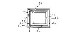
図4は、同一平面構造のアンテナの実施の形態を示したものであり、平面構造(四角形)の二次元導体分布1の全ての周辺に、一次元導体分布2a,2bと一次元空隙分布3a,3bが交互に層構造に配置してアンテナを構成したものである。 FIG. 4 shows an embodiment of an antenna having the same planar structure. One-dimensional conductor distributions 2a and 2b and a one-dimensional gap distribution 3a are formed around all of the two-
このアンテナは、図5に示すように、二次元導体分布1と内側一次元導体分布2aが導体接続部4aを用いて、その導体接続部4aの反対側で内側一次元導体分布2aと外側一次元導体分布2bが導体接続部4bを用いて層間接続され、また、一次元導体分布2a,2bが導体切断部5a,5bを用いて切断される。給電部6は、二次元導体分布1と内側一次元導体分布2a間に接続される。 As shown in FIG. 5, in this antenna, the two-
この結果として、伝送線路及び浮遊線路で表現されるアンテナエレメントが構成される。二次元導体分布1は接地導体と見なすことができ、この図5の構造であれば、伝送線路と浮遊線路を用いて図6のように表現される。すなわち、伝送線路は、導体切断部5aにより内側一次元導体分布2aで形成されるオープンスタブ7a1 ,7a2 、導体切断部5bにより外側一次元導体分布2bで形成されるオープンスタブ7b1 ,7b2 、導体接続部4aで形成されるショートスタブ8、ショートスタブ8と給電部6を結ぶ内側一次元導体分布2aで形成される結合線路9a1 、導体接続部4bで形成される結合線路9b、結合線路9bと給電部6を結ぶ内側一次元導体分布2aで形成される結合線路9a2 である。As a result, an antenna element expressed by a transmission line and a floating line is configured. The two-
この同一平面構造のアンテナもアンテナエレメントを構成する複数の伝送線路及び浮遊線路が、層構造に集約されており、所望の周波数の電波を放射するために必要なエレメントを小面積に構成することができ、また、同一のアンテナエレメントが複数の周波数の電波を共通して空間に放射するため、各々の周波数の電波を放射する複数のアンテナエレメントを電磁気的な干渉がないように離して配置する必要がない。 This coplanar antenna also has a plurality of transmission lines and floating lines that constitute an antenna element, which are aggregated in a layer structure, and it is possible to configure an element necessary for radiating a radio wave of a desired frequency in a small area. In addition, because the same antenna element radiates radio waves of multiple frequencies to the space in common, it is necessary to place multiple antenna elements that radiate radio waves of each frequency apart so as not to cause electromagnetic interference There is no.
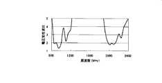
図7は、2.4GHz帯と5.5GHz帯の電波を送受信するアンテナの他の実施形態を示したもので、四角形状に形成した二次元導体分布1の外周に一次元空隙分布3aを介して内側一次元導体分布2aを配置し、その一次元導体分布2aの外周に一次元空隙分布3bを介して一次元導体分布2bを配置して層構造とし、二次元導体分布1と内側一次元導体分布2aを導体接続部4aで接続し、内側一次元導体分布2aと外側一次元導体分布2bを導体接続部4bで接続し、内側一次元導体分布2aに導体切断部5a1 ,5a2 を形成し、外側一次元導体分布2bに導体切断部5bを形成し、外側一次元導体分布2bに給電部6を接続した構成である。FIG. 7 shows another embodiment of an antenna for transmitting and receiving radio waves in the 2.4 GHz band and the 5.5 GHz band, and the outer periphery of the two-
図8は、図7のアンテナの電圧定在波比であり、上記二つの周波数の電波を空間に放射するために、給電部との良好なインピーダンス整合が実現されている。 図9は、図7のアンテナの電流強度分布である。白色の部分が、電流強度が大きく電波の放射に寄与する部分であり、2.4GHz帯では、図9(a)に示すように、導体接続部4bの左右に位置した外側一次元導体分布2bの部分と給電部6の左右に位置した外側一次元導体分布2bの部分に電流強度の大きい部分が存在し、5.5GHz帯では、図9(b)に示すように、導体接続部4bから給電部6を通して導体切断部5bに至る外側一次元導体分布2bの部分に電流強度の大きい部分が存在しており、2.4GHz帯と5.5GHz帯で、共通して電流強度の大きい部分が存在する。 FIG. 8 shows the voltage standing wave ratio of the antenna shown in FIG. 7. In order to radiate radio waves having the above two frequencies to the space, good impedance matching with the power feeding unit is realized. FIG. 9 is a current intensity distribution of the antenna of FIG. The white portion is a portion that has a large current intensity and contributes to the emission of radio waves. In the 2.4 GHz band, as shown in FIG. 9A, the outer one-dimensional conductor distribution 2b positioned on the left and right of the conductor connecting portion 4b. 9 and a portion of the outer one-dimensional conductor distribution 2b located on the left and right of the
これは、同一のアンテナエレメントが共通して複数の周波数の電波を放射することを示す。よって、従来技術とは異なり、各々の周波数の電波を放射する複数のアンテナエレメントを電磁気的な干渉がないように離して配置する必要がなく、アンテナの小型化に関して大きな効果を得ることができる。 This indicates that the same antenna element radiates radio waves having a plurality of frequencies in common. Therefore, unlike the prior art, it is not necessary to dispose a plurality of antenna elements that radiate radio waves of each frequency so as not to cause electromagnetic interference, and a great effect can be obtained with respect to miniaturization of the antenna.
以上のように、本発明のアンテナは、アンテナエレメントが層構造に集約されており、マルチバンドアンテナの小型化に関して大きな効果を得ることができる。さらに、同一のアンテナエレメントが複数の周波数の電波を共通して放射するため、各々の周波数の電波を放射する複数のアンテナエレメントを離して配置する必要がなく、マルチバンドアンテナの小型化に関して大きな効果を得ることができる。 As described above, in the antenna of the present invention, the antenna elements are concentrated in a layer structure, and a great effect can be obtained with respect to downsizing of the multiband antenna. In addition, since the same antenna element radiates radio waves of multiple frequencies in common, it is not necessary to place multiple antenna elements that radiate radio waves of each frequency apart from each other. Can be obtained.
以上、図1〜図9により本発明のアンテナの基本的な構成を説明したが、本発明は、上述の形態に限らず、一次元導体分布2及び一次元空隙分布3が、二層から五層の層構造としても良い。層数を多くすることで、より多くのアンテナエレメントを集約することができ、アンテナの小型化に効果がある。層数が五層を超えると、伝送線路及び浮遊線路と接地導体との距離が大きくなるためにアンテナの設計が難しくなり、さらにアンテナの機械的強度が低下するため、五層以下にすることが望ましい。 As described above, the basic configuration of the antenna of the present invention has been described with reference to FIGS. 1 to 9. However, the present invention is not limited to the above-described form, and the one-
また、導体接続部4及び導体切断部5は、各層ごとに三箇所以下であることが望ましい。導体接続部4及び導体切断部5の数を増やすことで、複雑な構造のアンテナエレメントが得られ、より多くの周波数の電波を放射することが可能となるが、導体接続部4が多すぎると、閉じた電流経路が増えるために電波の放射に必要な共振長が得にくくなり、導体切断部5が多すぎると、浮遊線路が増えるために機械的強度が低下する。 Moreover, as for the
本発明は、一次元導体分布2、一次元空隙分布3、及び二次元導体分布1からなるアンテナの外形が概ね四角形であることが好ましい。アンテナの外形が四角形であることで、アンテナの製造及び無線端末への実装が容易になる。 In the present invention, it is preferable that the outer shape of the antenna composed of the one-
さらに一次元導体分布2及び二次元導体分布1は、一体導体からなることが好ましい。アンテナを一体導体とすることで、低コストで量産性に優れた打ち抜き工程を用いて製造することができる。加えて、アンテナが一体導体からなることで、アンテナを無線端末に実装する際の取り扱いが容易になる。 Furthermore, the one-
一次元導体分布2、一次元空隙分布3、及び二次元導体分布1は、打ち抜き工程、又はメッキ工程、又はエッチング工程により製造されることが好ましい。汎用的な金属加工工程である、打ち抜き工程、メッキ工程、エッチング工程を用いることで、アンテナの製造が容易になり、製造コストを低減することができる。 The one-
一次元導体分布2、一次元空隙分布3、及び二次元導体分布1は、リジッド基板上に作製されることが好ましい。これは、リジッド基板の誘電体による波長短縮効果により、アンテナをより小型化する効果がある。 The one-
一次元導体分布2、一次元空隙分布3、及び二次元導体分布1は、可撓性のあるフレキ基板上に作製されることが好ましい。フレキ基板上に作製することで、アンテナを屈曲させることができ、無線端末への内蔵を容易にすることができる。 The one-
一次元導体分布2、一次元空隙分布3、及び二次元導体分布1が基台上に作製されることが好ましい。機械的強度のある基台上に作製することにより、無線端末への実装を容易にすることができる。 It is preferable that the one-
一次元導体分布2、一次元空隙分布3、及び二次元導体分布1は、誘電体シートでラミネートされることが好ましい。ラミネートすることで、金属腐食などの経年劣化を防ぐことができ、長期間にわたり安定したアンテナ特性を得ることができる。 The one-
二次元導体分布2は、回路基板の接地導体又は無線端末の金属部品であることが好ましい。これにより、二次元導体分布の電気的面積を拡大することができ、より安定した接地導体が得られ、良好なアンテナ特性を得ることができる。 The two-
給電部6には、同軸ケーブル又はコンタクトピンを用いることが好ましい。これにより、高周波電力の低損失な給電が可能となる。 A coaxial cable or a contact pin is preferably used for the
本発明のアンテナは、携帯電話等の無線端末に内蔵させるが、この場合、液晶ディスプレイ上部、又はキーパッド下部、又はヒンジ部に内蔵させる。液晶ディスプレイ上部、キーパッド下部、ヒンジ部にアンテナを内蔵することで、使用者の手の影響によるアンテナ性能劣化を抑えることができ、携帯電話の電波送受信特性を高めることができる。 The antenna of the present invention is built in a wireless terminal such as a mobile phone. In this case, the antenna is built in the upper part of the liquid crystal display, the lower part of the keypad, or the hinge part. By incorporating an antenna in the upper part of the liquid crystal display, the lower part of the keypad, and the hinge part, it is possible to suppress deterioration of the antenna performance due to the influence of the user's hand, and to improve the radio wave transmission / reception characteristics of the mobile phone.
上述した本発明のアンテナのより具体的な実施形態を説明する。 A more specific embodiment of the antenna of the present invention described above will be described.
図10及び図11に、本発明の第1の実施形態を示した。 10 and 11 show a first embodiment of the present invention.
図10は、本発明のアンテナA1であり、無線LANに用いる2.4GHz帯と5.5GHz帯の電波を放射するアンテナである。 FIG. 10 shows the antenna A1 according to the present invention, which radiates radio waves in the 2.4 GHz band and the 5.5 GHz band used for the wireless LAN.
平面構造で四角形の二次元導体分布1が構成され、二次元導体分布1の全ての周辺に、内側一次元空隙分布3aを介して枠状の内側一次元導体分布2aが配置され、内側一次元導体分布2aの周辺に、外側一次元空隙分布3bを介して外側一次元導体分布2bが配置され、一次元導体分布2と一次元空隙分布3が二層構造で構成されている。 A rectangular two-
各層ごとに、すなわち二次元導体分布1と内側一次元導体分布2aが、導体接続部4a1 ,4a2 を用いて、内側一次元導体分布2aと外側一次元導体分布2bが導体接続部4b1 ,4b2 ,4b3 を用いて層間接続されている。内側の導体接続部4a1 と外側の導体接続部4b1 は、四角形の二次元導体分布1の上辺から連続するよう、同じく内側の導体接続部4a2 と外側の導体接続部4b2 は、二次元導体分布1の下辺から連続するように設けられて各層を接続する。For each layer, that is, the two-
また各層ごとに、すなわち、内側一次元導体分布2aが、導体切断部5a1 ,5a2 を用いて切断され、外側一次元導体分布2bが、導体切断部5b1 ,5b2 ,5b3 を用いて切断されている。内側の導体切断部5a1 は、枠状の内側一次元導体分布2aの下辺右隅を、他方の導体切断部5a2 は、内側一次元導体分布2aの上辺左隅を切断するように形成される。外側の導体切断部5b1 は、枠状の外側一次元導体分布2bの上辺右隅を、導体切断部5b2 は、外側一次元導体分布2bの左辺中央部を、導体切断部5b3 は、外側一次元導体分布2bの下辺の中央やや左側を切断するように形成される。Further, for each layer, that is, the inner one-dimensional conductor distribution 2a is cut using the conductor cut portions 5a1 and 5a2 , and the outer one-dimensional conductor distribution 2b uses the conductor cut portions 5b1 , 5b2 , and 5b3 . Disconnected. The inner conductor cut portion 5a1 is formed so as to cut the lower right corner of the frame-shaped inner one-dimensional conductor distribution 2a, and the other conductor cut portion 5a2 is formed so as to cut the upper left corner of the inner one-dimensional conductor distribution 2a. . The outer conductor cut portion 5b1 is the upper right corner of the frame-like outer one-dimensional conductor distribution 2b, the conductor cut portion 5b2 is the center of the left side of the outer one-dimensional conductor distribution 2b, and the conductor cut portion 5b3 is The outer one-dimensional conductor distribution 2b is formed so as to cut the middle and the left side of the lower side.
給電部6は、導体切断部5a1 ,5b1 の位置の内側一次元導体分布2aに給電するように接続され、そのインピーダンスは50Ωである。The
図11に、図10のアンテナの電圧定在波比を示す。 FIG. 11 shows the voltage standing wave ratio of the antenna of FIG.
無線LANでは、電圧定在波比が2以下であれば良好な送受信が可能であるが、図10のアンテナA1は、2.4GHz帯、5.5GHz帯ともに電圧定在波比が2以下であり、良好な送受信が可能である。 In the wireless LAN, good transmission / reception is possible if the voltage standing wave ratio is 2 or less, but the antenna A1 in FIG. 10 has a voltage standing wave ratio of 2 or less in both the 2.4 GHz band and the 5.5 GHz band. Yes, good transmission / reception is possible.
このように、本発明のアンテナは、二つの異なる周波数の電波送受信に用いて好適なアンテナである。 Thus, the antenna of the present invention is a suitable antenna for use in radio wave transmission / reception at two different frequencies.
図12及び図13に、本発明の第2の実施形態を示す。 12 and 13 show a second embodiment of the present invention.
図12は、本発明のアンテナA2であり、携帯電話に用いる900MHz帯と2GHz帯の電波を放射するアンテナである。 FIG. 12 shows the antenna A2 of the present invention, which is an antenna that radiates 900 MHz band and 2 GHz band radio waves used in mobile phones.
回路基板11の接地導体が二次元導体分布1であり、回路基板の一端に、一次元導体分布2a,2b,2c,2dと一次元空隙分布3a,3b,3c,3dが四層構造で構成されている。 The ground conductor of the
各層ごとに、二次元導体分布1及び一次元導体分布2が、導体接続部4を用いて層間接続されている。 For each layer, the two-
すなわち、二次元導体分布1と一番目の一次元導体分布2aが第1の導体接続部4aで、一番目の一次元導体分布2aと二番目の一次元導体分布2bの中央が第2の導体接続部4bで、二番目の一次元導体分布2bと三番目の一次元導体分布2cの両端部が第3の導体接続部4c1 ,4c2 で、三番目の一次元導体分布2cと四番目の一次元導体分布2dの両端部が第4の導体接続部4d1 ,4d2 で、それぞれ接続されている。That is, the two-
また、各層ごとに、一次元導体分布2が、導体切断部5を用いて切断されている。本実施の形態においては、一番目と四番目の一次元導体分布2a,2dを除き、二番目と三番目の一次元導体分布2b,2cの略中央に導体切断部5b、5cが形成されるが、一番目と四番目の一次元導体分布2a,2dに導体切断部5を形成するようにしても良い。 Further, for each layer, the one-
給電部6は、一番目の一次元導体分布2aに接続されており、そのインピーダンスは50Ωである。 The
図13に、図12のアンテナA2の電圧定在波比を示す。 FIG. 13 shows the voltage standing wave ratio of the antenna A2 of FIG.
携帯電話では、電圧定在波比が3以下であれば良好な送受信が可能であるが、図12のアンテナA2は900MHz帯、2GHz帯ともに電圧定在波比が3以下であり、良好な送受信が可能である。このように、二次元導体分布に無線端末の回路基板の接地導体を用いることで、より安定した接地導体となり、良好なアンテナ特性を得ることができる。また、層数を増やすことで、アンテナエレメントをさらに集約する効果がある。 With a cellular phone, good transmission / reception is possible if the voltage standing wave ratio is 3 or less, but the antenna A2 in FIG. 12 has a voltage standing wave ratio of 3 or less in both the 900 MHz band and 2 GHz band, and good transmission / reception. Is possible. Thus, by using the ground conductor of the circuit board of the wireless terminal for the two-dimensional conductor distribution, a more stable ground conductor can be obtained, and good antenna characteristics can be obtained. Further, there is an effect of further collecting the antenna elements by increasing the number of layers.
図14に、本発明の第3の実施形態を示す。 FIG. 14 shows a third embodiment of the present invention.
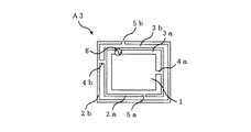
図14は、本発明のアンテナA3であり、アンテナエレメントが一体化した導体で構成されている。 FIG. 14 shows the antenna A3 of the present invention, which is composed of a conductor in which antenna elements are integrated.
このアンテナA3は、図5で説明したアンテナと同じ構成であり、同一部材に同一の符号を付し、その説明は省略する。 The antenna A3 has the same configuration as the antenna described in FIG. 5, and the same reference numerals are given to the same members, and the description thereof is omitted.
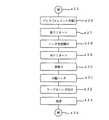
本発明のアンテナA3は、打ち抜き工程を用いて作製される。打ち抜き工程は図15に示す工程からなる。 The antenna A3 of the present invention is manufactured using a punching process. The punching process includes a process shown in FIG.
すなわち、始めs1に、プレス工程s2で導体からアンテナA3の形状に打ち抜き、サビ止め等の表面処理s3を行って終了s4する。 That is, at the beginning s1, the pressing process s2 punches out the conductor into the shape of the antenna A3, performs a surface treatment s3 such as rusting, and ends s4.
このように、アンテナを一体化した導体で構成して打ち抜き工程を用いて作製することで、アンテナの作製を容易にし、アンテナを安価にすることができる。 In this manner, by forming the antenna with an integrated conductor and using a punching process, the antenna can be easily manufactured and the antenna can be inexpensive.
図16に、本発明の第4の実施形態を示す。 FIG. 16 shows a fourth embodiment of the present invention.
図16は、本発明のアンテナA4であり、図14と図5で説明したアンテナA3のアンテナエレメントを誘電体シート12でラミネートしたものである。誘電体シート12はポリイミド系の材料を用いている。 FIG. 16 shows the antenna A4 of the present invention, in which the antenna element of the antenna A3 described with reference to FIGS. 14 and 5 is laminated with the dielectric sheet 12. The dielectric sheet 12 is made of a polyimide material.
このように、アンテナエレメントを誘電体シートでラミネイトすることで、金属腐食などの経年劣化を防ぐことができ、長期間にわたり安定したアンテナ特性を得ることができる。 As described above, by laminating the antenna element with the dielectric sheet, it is possible to prevent deterioration over time such as metal corrosion and to obtain stable antenna characteristics over a long period of time.
図17に、本発明の第5の実施形態を示す。 FIG. 17 shows a fifth embodiment of the present invention.
図17は、本発明のアンテナA5であり、図14と図5で説明したアンテナA3のアンテナエレメントをリジッド基板13上にエッチング工程を用いて作製したものである。 FIG. 17 shows an antenna A5 according to the present invention, in which the antenna element of the antenna A3 described with reference to FIGS. 14 and 5 is formed on a
エッチング工程は図18に示す工程からなる。 The etching process includes the process shown in FIG.
始めs5に、金属張りの基板にレジストを塗布s6し、アンテナ形成用のマスクで、マスキングs7を行い、紫外線露光s8を行って現像処理s9し、エッチングs10を行った後、レジスト膜を剥離s11してエッチング工程を終了s12する。 First, in s5, a resist is applied to a metal-clad substrate s6, masking s7 is performed with a mask for antenna formation, ultraviolet exposure s8 is performed, development processing s9 is performed, etching s10 is performed, and then the resist film is stripped s11. Then, the etching process is terminated s12.
このように、アンテナエレメントを、エッチング工程を用いて作製することで、アンテナの作製を容易にして、アンテナを安価にすることができる。さらに、リジッド基板の誘電体による波長短縮効果により、アンテナをさらに小型化することができる。 Thus, by manufacturing the antenna element using the etching process, the antenna can be easily manufactured and the antenna can be inexpensive. Furthermore, the antenna can be further downsized due to the wavelength shortening effect by the dielectric of the rigid substrate.
図19に、本発明の第6の実施形態を示す。 FIG. 19 shows a sixth embodiment of the present invention.
図19は、本発明のアンテナA6であり、アンテナエレメントがフレキ基板14上にメッキ工程とエッチング工程を用いて作製されている。 FIG. 19 shows an antenna A6 of the present invention, in which an antenna element is formed on a
このアンテナエレメントは図2で説明したアンテナと同じ構成であり、同一部材に同一の符号を付し、その説明は省略する。 This antenna element has the same configuration as the antenna described in FIG. 2, and the same reference numerals are given to the same members, and the description thereof is omitted.
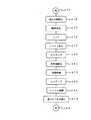
メッキ工程とエッチング工程は図20に示す工程からなる。 The plating process and the etching process consist of the processes shown in FIG.
このメッキ・エッチング工程は、始めs13に誘電体基板の表面粗面化処理s14を行った後、触媒を塗布s15し、表面にメッキs16を行った後、レジストを塗布s17し、アンテナ形成用のマスクで、マスキングs18を行い、紫外線露光s19を行って現像処理s20し、エッチングs21を行った後、レジスト膜を剥離s22して終了s23する。 In this plating / etching process, first, a surface roughening treatment s14 of the dielectric substrate is performed in s13, then a catalyst is applied s15, plating is performed on the surface, s16 is applied, and a resist is applied s17, thereby forming an antenna. Masking s18 is performed with a mask, ultraviolet exposure s19 is performed, development processing s20 is performed, etching s21 is performed, and then the resist film is peeled off s22 to finish s23.
このように、アンテナエレメントを、フレキ基板14上に作製することで、アンテナを屈曲させることができ、無線端末への内蔵を容易にすることができる。 In this manner, by manufacturing the antenna element on the
図21に、本発明の第7の実施形態を示す。 FIG. 21 shows a seventh embodiment of the present invention.
図21は、本発明のアンテナA7であり、曲面構造を持つ基台15の上に、メッキ工程を用いてアンテナ構造を作製している。 FIG. 21 shows an antenna A7 of the present invention, in which an antenna structure is produced on a base 15 having a curved structure using a plating process.
このアンテナA7のアンテナエレメントは、四角形状で基台15の面に沿った二次元導体分布1に一次元空隙分布3aを介して一次元導体分布2aを配置し、一次元導体分布2aに一次元空隙分布3bを介して一次元導体分布2bを配置して層構造とし、二次元導体分布1と一次元導体分布2aの端部を導体接続部4aで接続し、一次元導体分布2aと一次元導体分布2bの中央部を導体接続部4aで接続し、一次元導体分布2bに給電部6を接続したものである。 The antenna element of the antenna A7 has a rectangular shape, and a one-dimensional conductor distribution 2a is arranged in a two-
このように、本発明のアンテナは、曲面構造上にも作製可能であり、多様な形状に実装して好適なアンテナである。また、機械的強度のある基台上に作製することにより、無線端末への実装を容易にすることができる。 As described above, the antenna of the present invention can be manufactured on a curved surface structure, and is suitable for mounting in various shapes. In addition, by manufacturing on a base having mechanical strength, mounting on a wireless terminal can be facilitated.
図22に、本発明の第8の実施形態を示す。 FIG. 22 shows an eighth embodiment of the present invention.
図22は、本発明のアンテナA8であり、図16で説明したようにアンテナが誘電体シート12によってラミネートされ、給電部として、同軸ケーブル16を用いてハンダ接続したものであり、同一部材には同一符号を付し説明は省略するが、同軸ケーブル16は、その中心導体17が内側一次元導体分布2aに接続され、外導体18が二次元導体分布1に接続されている。 FIG. 22 shows the antenna A8 according to the present invention, in which the antenna is laminated by the dielectric sheet 12 as described in FIG. 16, and is soldered using the
以上のアンテナ作製の工程は、図23に示す工程からなる。 The above-described antenna manufacturing process includes the process shown in FIG.
始めs25に、プレス工程s26にてエレメント作製を行い、そのエレメントに誘電体シートを仮ラミネートs27し、その誘電体シートに、同軸ケーブルの接続部に位置した部分にハンダ用窓開けs28を行った後、本ラミネートs29を行い、アンテナのエレメント形状に枠取りs30を行い、ハンダ用窓に予備ハンダ付けs31を行い、しかる後、ケーブルハンダ付けs32を行い、洗浄s33を行って工程を終了s34する。 First, in s25, an element was manufactured in a pressing step s26, a dielectric sheet was temporarily laminated s27 on the element, and a solder window s28 was formed on the dielectric sheet at a portion located at the connection portion of the coaxial cable. Thereafter, this laminate s29 is performed, the frame shape s30 is formed in the antenna element shape, the preliminary soldering s31 is performed on the solder window, and then the cable soldering s32 is performed, the cleaning s33 is performed, and the process is completed s34 .
このように、給電部に同軸ケーブルを用いることで、高周波電力の低損失な給電が可能となる。 Thus, by using a coaxial cable for the power feeding unit, it is possible to feed high-frequency power with low loss.
図24に、本発明の第9の実施形態を示す。 FIG. 24 shows a ninth embodiment of the present invention.
図24は、本発明のアンテナA9であり、図21で説明したアンテナの一次元導体分布2bに給電部6を設けるにおいて、一次元導体分布2bに導体切断部5を形成すると共に導体切断部5の一次元導体分布2bの端部に給電接続部19a,19bが設けられ、コンタクトピン20a,20bを用いて給電している。 FIG. 24 shows the antenna A9 of the present invention. In providing the feeding
基台15は回路基板11にネジ止め(図示せず)で固定される。 The
以上のアンテナ作製と実装は、図25に示す工程からなる。 The antenna fabrication and mounting described above consist of the steps shown in FIG.
始めs35に基台15の表面粗面化処理s36を行った後、触媒を塗布s37し、表面にメッキs38を行った後、レジストを塗布s39し、アンテナ形成用のマスクで、マスキングs40を行い、紫外線露光s41を行って現像処理s42し、エッチングs43を行った後、レジスト膜を剥離s44してアンテナを形成し、その基台を回路基板11にネジ止め固定s45を行って終了s46する。 First, after surface roughening treatment s36 of the
このように、給電部にコンタクトピン20a,20bを用いることで、低損失の給電が可能となり、加えて高密度のアンテナ実装が可能となる。 As described above, by using the contact pins 20a and 20b in the power feeding section, it is possible to feed power with low loss and to mount a high-density antenna.
図26に、本発明の第10の実施形態を示す。 FIG. 26 shows a tenth embodiment of the present invention.
図26は、本発明のアンテナA10であり、二次元導体分布1に一次元空隙分布3aを介して一次元導体分布2aを配置し、一次元導体分布2aに一次元空隙分布3bを介して一次元導体分布2bを配置して層構造とし、二次元導体分布1と一次元導体分布2aの端部を導体接続部4aで接続し、一次元導体分布2aと一次元導体分布2bの略中央部を導体接続部4bで接続し、二次元導体分布1と一次元導体分布2aに給電部6を接続したものである。 FIG. 26 shows an antenna A10 according to the present invention, in which a one-dimensional conductor distribution 2a is arranged in a two-
本実施の形態では、二次元導体分布1に無線端末の金属部品21を用いている。二次元導体分布1と金属部品21は、銅テープ22を用いて導体接続されている。 このように、二次元導体分布の一部に無線端末の金属部品を用いることで、二次元導体分布の電気的面積を拡大することができ、より安定した接地導体が得られ、アンテナ特性を改善することが可能となる。 In the present embodiment, the metal component 21 of the wireless terminal is used for the two-
図27に、本発明の第11の実施形態を示す。 FIG. 27 shows an eleventh embodiment of the present invention.
図27は、本発明のアンテナA11であり、携帯電話23用のアンテナである。回路基板11上のアンテナ設置領域24に、図12で説明したアンテナA2が設けられ、液晶ディスプレイ25の上部に内蔵されている。 FIG. 27 shows the antenna A11 of the present invention, which is an antenna for the
このように、本発明のアンテナを携帯電話の液晶ディスプレイの上部に内蔵することにより、使用者の手の影響によるアンテナ性能劣化を防ぐことができ、携帯電話の電波送受信特性を高めることができる。 As described above, by incorporating the antenna of the present invention in the upper part of the liquid crystal display of the mobile phone, it is possible to prevent deterioration of the antenna performance due to the influence of the user's hand, and to improve the radio wave transmission / reception characteristics of the mobile phone.
図28に、本発明の第12の実施形態を示す。 FIG. 28 shows a twelfth embodiment of the present invention.
図28は、本発明のアンテナA12であり、携帯電話23用のアンテナである。回路基板11上のアンテナ設置領域24に、図12で説明したアンテナA2が設けられ、キーパッド26の下部に内蔵されている。 FIG. 28 shows the antenna A12 of the present invention, which is an antenna for the
このように、本発明のアンテナを携帯電話のキーパッドの下部に内蔵することにより、使用者の手の影響によるアンテナ性能劣化を防ぐことができ、携帯電話の電波送受信特性を高めることができる。 Thus, by incorporating the antenna of the present invention under the keypad of the mobile phone, it is possible to prevent the antenna performance from being deteriorated due to the influence of the user's hand, and to improve the radio wave transmission / reception characteristics of the mobile phone.
図29に、本発明の第13の実施形態を示す。 FIG. 29 shows a thirteenth embodiment of the present invention.
図29は、本発明のアンテナA13であり、携帯電話23用のアンテナである。回路基板11上のアンテナ設置領域24に、図24で説明したアンテナA9が設けられ、ヒンジ27の下部に内蔵されている。 FIG. 29 shows the antenna A13 of the present invention, which is an antenna for the
このように、本発明のアンテナを携帯電話のヒンジ部に内蔵することにより、使用者の手の影響によるアンテナ性能劣化を防ぐことができ、携帯電話の電波送受信特性を高めることができる。 As described above, by incorporating the antenna of the present invention in the hinge portion of the mobile phone, it is possible to prevent deterioration of the antenna performance due to the influence of the user's hand, and to improve the radio wave transmission / reception characteristics of the mobile phone.
1 二次元導体分布
2 一次元導体分布
3 一次元空隙分布
4 導体接続部
5 導体切断部
6 給電部
7 オープンスタブ
8 ショートスタブ
9 結合線路
10 浮遊線路
DESCRIPTION OF
Claims (15)
Translated fromJapaneseA mobile phone comprising the antenna according to claim 6 incorporated in an upper part of a liquid crystal display, a lower part of a keypad or a hinge part.
Priority Applications (1)
| Application Number | Priority Date | Filing Date | Title |
|---|---|---|---|
| JP2004304367AJP4325532B2 (en) | 2004-10-19 | 2004-10-19 | Antenna, manufacturing method thereof, and wireless terminal using the antenna |
Applications Claiming Priority (1)
| Application Number | Priority Date | Filing Date | Title |
|---|---|---|---|
| JP2004304367AJP4325532B2 (en) | 2004-10-19 | 2004-10-19 | Antenna, manufacturing method thereof, and wireless terminal using the antenna |
Publications (2)
| Publication Number | Publication Date |
|---|---|
| JP2006121190Atrue JP2006121190A (en) | 2006-05-11 |
| JP4325532B2 JP4325532B2 (en) | 2009-09-02 |
Family
ID=36538694
Family Applications (1)
| Application Number | Title | Priority Date | Filing Date |
|---|---|---|---|
| JP2004304367AExpired - Fee RelatedJP4325532B2 (en) | 2004-10-19 | 2004-10-19 | Antenna, manufacturing method thereof, and wireless terminal using the antenna |
Country Status (1)
| Country | Link |
|---|---|
| JP (1) | JP4325532B2 (en) |
Cited By (2)
| Publication number | Priority date | Publication date | Assignee | Title |
|---|---|---|---|---|
| JP2010259048A (en)* | 2009-04-02 | 2010-11-11 | Sony Computer Entertainment Inc | Information communication device and antenna |
| JP2011146971A (en)* | 2010-01-15 | 2011-07-28 | Nec Corp | Flexible substrate antenna and portable radio apparatus |
Citations (11)
| Publication number | Priority date | Publication date | Assignee | Title |
|---|---|---|---|---|
| JPH01147905A (en)* | 1987-12-03 | 1989-06-09 | Antenna Giken Kk | Plane antenna |
| JP2000040917A (en)* | 1997-06-18 | 2000-02-08 | Kyocera Corp | Wide-angle circularly polarized antenna |
| JP2002319809A (en)* | 2001-04-24 | 2002-10-31 | Ee C Ii Tec Kk | Antenna device |
| JP3094677U (en)* | 2002-12-16 | 2003-07-04 | アルプス電気株式会社 | Two-band inverted F antenna |
| JP2003198410A (en)* | 2001-12-27 | 2003-07-11 | Matsushita Electric Ind Co Ltd | Antenna for communication terminal equipment |
| WO2003096475A1 (en)* | 2002-05-09 | 2003-11-20 | Koninklijke Philips Electronics N.V. | Antenna arrangement and module including the arrangement |
| JP2004040596A (en)* | 2002-07-05 | 2004-02-05 | Matsushita Electric Ind Co Ltd | Multi-frequency antenna for portable radio |
| JP2004048119A (en)* | 2002-07-09 | 2004-02-12 | Hitachi Cable Ltd | Plate-shaped multiple antenna and electric device having the same |
| JP2004504747A (en)* | 2000-07-13 | 2004-02-12 | トムソン ライセンシング ソシエテ アノニム | Multi-band planar antenna |
| JP2004128660A (en)* | 2002-09-30 | 2004-04-22 | Matsushita Electric Ind Co Ltd | Antenna device |
| JP2004201278A (en)* | 2002-12-06 | 2004-07-15 | Sharp Corp | Pattern antenna |
- 2004
- 2004-10-19JPJP2004304367Apatent/JP4325532B2/ennot_activeExpired - Fee Related
Patent Citations (11)
| Publication number | Priority date | Publication date | Assignee | Title |
|---|---|---|---|---|
| JPH01147905A (en)* | 1987-12-03 | 1989-06-09 | Antenna Giken Kk | Plane antenna |
| JP2000040917A (en)* | 1997-06-18 | 2000-02-08 | Kyocera Corp | Wide-angle circularly polarized antenna |
| JP2004504747A (en)* | 2000-07-13 | 2004-02-12 | トムソン ライセンシング ソシエテ アノニム | Multi-band planar antenna |
| JP2002319809A (en)* | 2001-04-24 | 2002-10-31 | Ee C Ii Tec Kk | Antenna device |
| JP2003198410A (en)* | 2001-12-27 | 2003-07-11 | Matsushita Electric Ind Co Ltd | Antenna for communication terminal equipment |
| WO2003096475A1 (en)* | 2002-05-09 | 2003-11-20 | Koninklijke Philips Electronics N.V. | Antenna arrangement and module including the arrangement |
| JP2004040596A (en)* | 2002-07-05 | 2004-02-05 | Matsushita Electric Ind Co Ltd | Multi-frequency antenna for portable radio |
| JP2004048119A (en)* | 2002-07-09 | 2004-02-12 | Hitachi Cable Ltd | Plate-shaped multiple antenna and electric device having the same |
| JP2004128660A (en)* | 2002-09-30 | 2004-04-22 | Matsushita Electric Ind Co Ltd | Antenna device |
| JP2004201278A (en)* | 2002-12-06 | 2004-07-15 | Sharp Corp | Pattern antenna |
| JP3094677U (en)* | 2002-12-16 | 2003-07-04 | アルプス電気株式会社 | Two-band inverted F antenna |
Cited By (3)
| Publication number | Priority date | Publication date | Assignee | Title |
|---|---|---|---|---|
| JP2010259048A (en)* | 2009-04-02 | 2010-11-11 | Sony Computer Entertainment Inc | Information communication device and antenna |
| US9048531B2 (en) | 2009-04-02 | 2015-06-02 | Sony Corporation | Information communication device and antenna |
| JP2011146971A (en)* | 2010-01-15 | 2011-07-28 | Nec Corp | Flexible substrate antenna and portable radio apparatus |
Also Published As
| Publication number | Publication date |
|---|---|
| JP4325532B2 (en) | 2009-09-02 |
Similar Documents
| Publication | Publication Date | Title |
|---|---|---|
| US11139574B2 (en) | Antennaless wireless device | |
| US20220077581A1 (en) | Antennaless Wireless Device | |
| US7755545B2 (en) | Antenna and method of manufacturing the same, and portable wireless terminal using the same | |
| JP4868128B2 (en) | ANTENNA DEVICE AND RADIO COMMUNICATION DEVICE USING THE SAME | |
| CN102709687B (en) | Antenna device | |
| JP4003077B2 (en) | Antenna and wireless communication device | |
| JP4301034B2 (en) | Wireless device with antenna | |
| CN203747020U (en) | Built-in Antenna for Portable Terminals | |
| US8462056B2 (en) | Built-in antenna for portable terminal | |
| JP4232158B2 (en) | ANTENNA DEVICE AND COMMUNICATION DEVICE USING THE SAME | |
| JP2009021932A (en) | Electronic device and manufacturing method thereof | |
| JP2003101335A (en) | Antenna device and communication device using the same | |
| US20070057849A1 (en) | Antenna for dual band operation | |
| JPH10209738A (en) | Inverted e-type antenna | |
| JP2012518300A (en) | Antenna configuration, printed circuit board, portable electronic device, and conversion kit | |
| CN105075005A (en) | Space saving multiband antenna | |
| JP2005535239A (en) | Dual band antenna system | |
| JP3586915B2 (en) | Vehicle antenna device | |
| JP4073789B2 (en) | Dielectric antenna and mobile communication device incorporating the same | |
| WO2004025781A1 (en) | Loop antenna | |
| JP3467164B2 (en) | Inverted F antenna | |
| JP4325532B2 (en) | Antenna, manufacturing method thereof, and wireless terminal using the antenna | |
| JP2004096314A (en) | Dielectric antenna and mobile communication apparatus with built-in the same | |
| CN114628892B (en) | PCB antenna and electronic equipment | |
| JP4631288B2 (en) | Antenna module |
Legal Events
| Date | Code | Title | Description |
|---|---|---|---|
| A621 | Written request for application examination | Free format text:JAPANESE INTERMEDIATE CODE: A621 Effective date:20070119 | |
| A977 | Report on retrieval | Free format text:JAPANESE INTERMEDIATE CODE: A971007 Effective date:20081030 | |
| A131 | Notification of reasons for refusal | Free format text:JAPANESE INTERMEDIATE CODE: A131 Effective date:20081104 | |
| A521 | Written amendment | Free format text:JAPANESE INTERMEDIATE CODE: A523 Effective date:20081217 | |
| A131 | Notification of reasons for refusal | Free format text:JAPANESE INTERMEDIATE CODE: A131 Effective date:20090414 | |
| A521 | Written amendment | Free format text:JAPANESE INTERMEDIATE CODE: A523 Effective date:20090424 | |
| TRDD | Decision of grant or rejection written | ||
| A01 | Written decision to grant a patent or to grant a registration (utility model) | Free format text:JAPANESE INTERMEDIATE CODE: A01 Effective date:20090519 | |
| A01 | Written decision to grant a patent or to grant a registration (utility model) | Free format text:JAPANESE INTERMEDIATE CODE: A01 | |
| A61 | First payment of annual fees (during grant procedure) | Free format text:JAPANESE INTERMEDIATE CODE: A61 Effective date:20090601 | |
| FPAY | Renewal fee payment (event date is renewal date of database) | Free format text:PAYMENT UNTIL: 20120619 Year of fee payment:3 | |
| R150 | Certificate of patent or registration of utility model | Free format text:JAPANESE INTERMEDIATE CODE: R150 | |
| LAPS | Cancellation because of no payment of annual fees |