JP2006120804A - Imaging apparatus and drive control method - Google Patents
Imaging apparatus and drive control methodDownload PDFInfo
- Publication number
- JP2006120804A JP2006120804AJP2004306144AJP2004306144AJP2006120804AJP 2006120804 AJP2006120804 AJP 2006120804AJP 2004306144 AJP2004306144 AJP 2004306144AJP 2004306144 AJP2004306144 AJP 2004306144AJP 2006120804 AJP2006120804 AJP 2006120804A
- Authority
- JP
- Japan
- Prior art keywords
- potential
- light receiving
- unit
- period
- electrode
- Prior art date
- Legal status (The legal status is an assumption and is not a legal conclusion. Google has not performed a legal analysis and makes no representation as to the accuracy of the status listed.)
- Granted
Links
Images


Landscapes
- Solid State Image Pick-Up Elements (AREA)
- Transforming Light Signals Into Electric Signals (AREA)
- Light Receiving Elements (AREA)
Abstract
Translated fromJapaneseDescription
Translated fromJapanese本発明は、CMOSセンサー等の撮像装置に係り、特に画素間をトレンチ分離した固体撮像装置の駆動制御方法に関する。 The present invention relates to an imaging device such as a CMOS sensor, and more particularly to a drive control method for a solid-state imaging device in which pixels are separated by trenches.
従来からCCD撮像素子においては低暗電流化のためにフォトダイオードとしてP+np型の埋め込みフォトダイオード構造が使われてきた。CMOSセンサーにおいても高S/N、高感度化のためにフォトダイオードとして埋め込み型を採用する場合が多くなっている。このCMOSセンサーでは受光部からの読み出しをCCDなどに比べ低電圧で行う必要があり、そのため埋め込みフォトダイオードのポテンシャルを深く設定することが難しかしく、受光部の取り扱い電荷量が少なくなる。 Conventionally, in a CCD image pickup device, a P + np type embedded photodiode structure has been used as a photodiode in order to reduce a dark current. Also in the CMOS sensor, a buried type is often used as a photodiode for high S / N and high sensitivity. In this CMOS sensor, it is necessary to read out from the light receiving portion at a lower voltage than a CCD or the like, so that it is difficult to set the potential of the embedded photodiode deeply, and the amount of charge handled by the light receiving portion is reduced.
上記受光部から低電圧で読み出すための埋め込みフォトダイオード構造として、フォトダイオードの電子蓄積層であるN層をホール蓄積層よりも読み出し電極側に張り出す構造が採用されている。このような構造にすることで、電子蓄積層の面積や電子蓄積層のトータルドーズが増すために、受光部の静電ポテンシャルをそれほど深くすることなしに、受光部の取り扱い電荷量を増大させることができる。また、読み出し電圧の増大を抑えるためには、受光部の静電ポテンシャルを深くしないことが肝要であるので、受光部の取り扱い電荷量を増大するためには電子蓄積層のN+層の面積や濃度をだけでなく、表面P+層と電子蓄積層の下のP層濃度を高める方法も採られる。 As a buried photodiode structure for reading out from the light receiving portion at a low voltage, a structure is adopted in which an N layer, which is an electron storage layer of the photodiode, is extended from the hole storage layer to the read electrode side. With this structure, the area of the electron storage layer and the total dose of the electron storage layer increase, so that the amount of charge handled by the light receiving unit can be increased without deepening the electrostatic potential of the light receiving unit. Can do. In order to suppress an increase in the read voltage, it is important not to deepen the electrostatic potential of the light receiving portion. Therefore, in order to increase the amount of charge handled by the light receiving portion, the area and concentration of the N + layer of the electron storage layer In addition to the above, a method of increasing the P layer concentration under the surface P + layer and the electron storage layer is also employed.
しかし、このような構造ではP+層とN+層の間の電界が増加し易く、電界の増大は暗電流や白点が増えるというディメリットがあった。またN層の張り出し部分では空乏層がシリコン/シリコン酸化膜界面に触れやすく、そのため暗電流が増大しやすいというディメリットがあった。さらに、CMOSセンサーでは画素のトランジスタエリアの縮小やチップ内周辺回路の小型化のために、素子分離構造としてSTI(浅いトレンチ分離)が用いられてきているが、STI構造ではSTI側面に暗電流抑制のためのP層が必要で、それゆえに電荷蓄積層であるN層の実効的面積を減少させ、受光部の取り扱い電荷量を減らす傾向にあるというディメリットがある。 However, in such a structure, the electric field between the P + layer and the N + layer is likely to increase, and the increase in the electric field has a disadvantage that dark current and white spots increase. In addition, the depletion layer easily touches the silicon / silicon oxide film interface at the overhanging portion of the N layer, so that there is a disadvantage that dark current is likely to increase. Furthermore, in CMOS sensors, STI (shallow trench isolation) has been used as an element isolation structure in order to reduce the pixel transistor area and downsize peripheral circuits in the chip, but in the STI structure, dark current suppression is performed on the side of the STI. Therefore, there is a disadvantage that the P layer for the light receiving portion is necessary, and therefore, the effective area of the N layer as the charge storage layer tends to be reduced and the amount of charge handled by the light receiving portion tends to be reduced.
図6は従来の一般的なCMOSセンサーの構成を示した断面図である。CMOSセンサーは、基板1に形成された画素領域Pウエル2内に、ホール蓄積層3、信号電荷蓄積N層4、読み出し領域5、読み出し部N+(FD)7及び浅いトレンチ分離(STI)のための溝10を形成して構成されている。溝10の内側の側壁はSi酸化膜などの絶縁材が充填され、その外側にSTI側壁P層9が形成されている。さらに読み出し領域5の上部には絶縁膜12を介して読み出しゲート6が、このゲート6に隣接してリセットゲート8が配置されている。このような一般的なCMOSセンサーの受光部は、基板最表面のホール蓄積層3とその下層に形成される信号電荷蓄積N層4から成る埋め込みフォトダイオードで構成されている。また、画素分離にはLOCOSを用いることもよくあるが、この図6ではSTIを用いた構成となっている(例えば特許文献1参照)。
図6に示したCMOSセンサーのタイプの制約はSTI側壁P層9のP層幅を暗電流対策上、或る幅以上(或る濃度以上)に確保する必要があるが、これによりフォトダイオードの信号電荷蓄積N層4の実効面積が減少して取り扱い電荷量が少なくなってしまう。そこで、単位面積あたりのフォトダイオード取り扱い電荷量を増大させるために信号電荷蓄積N層4のドナー濃度を上げると、ホール蓄積層3との電界が高まり、これによって白傷が発生し易くなったり、或いは読み出しゲート6の読み出しに高い電圧値を要するなどのディメリットがある。 The CMOS sensor type restriction shown in FIG. 6 requires that the P layer width of the STI side wall P layer 9 be secured to a certain width or more (a certain concentration or more) in order to prevent dark current. The effective area of the signal charge
本発明は前記事情に鑑み案出されたものであって、本発明の目的は、低暗電流、低読み出し電圧及び高い取り扱い電荷量を得ることができる埋め込みフォトダイオード及びトレンチ分離構造を備えた撮像装置及びこの撮像装置の駆動制御方法を提供することにある。 The present invention has been devised in view of the above circumstances, and an object of the present invention is to provide an imaging device including a buried photodiode and a trench isolation structure capable of obtaining a low dark current, a low readout voltage, and a high handling charge amount. An apparatus and a drive control method for the image pickup apparatus are provided.
本発明は上記目的を達成するため、受光して電荷を生成する受光部を含む複数の画素と、前記受光部に蓄積された電荷量を検出して画素信号を出力する信号検出部と、前記受光部の信号電荷を前記信号検出部に読み出す読み出し部と、前記複数の画素の画素間に設けられたトレンチ分離部と、前記トレンチ分離部の溝内に埋め込まれた埋め込み電極と、
前記埋め込み電極を駆動する駆動制御部とを具備し、前記駆動制御部は、受光蓄積期間の少なくとも一部において前記埋め込み電極を第1の電位とし、蓄積された電荷を前記読み出し部を介して前記信号検出部に読み出す読み出し期間の少なくとも一部において前記埋め込み電極を第2の電位とすることを特徴とする。In order to achieve the above-described object, the present invention provides a plurality of pixels including a light receiving unit that receives light and generates charges, a signal detection unit that detects a charge amount accumulated in the light receiving unit and outputs a pixel signal, A readout unit that reads the signal charge of the light receiving unit to the signal detection unit, a trench isolation unit provided between pixels of the plurality of pixels, a buried electrode embedded in a trench of the trench isolation unit,
A drive control unit that drives the embedded electrode, wherein the drive control unit sets the embedded electrode to a first potential in at least a part of a light receiving and accumulation period, and stores the accumulated charge through the readout unit. The embedded electrode is set to a second potential in at least a part of a reading period read out to the signal detection unit.
また、本発明の駆動制御部は、前記受光蓄積期間及び前記読み出し期間の前半は前記電荷生成部を形成するホール蓄積層を第3の電位とし、前記読み出し期間の後半は同ホール蓄積層を第4の電位とする制御を行うことを特徴とする。 In the drive control unit of the present invention, the hole accumulation layer forming the charge generation unit is set to a third potential in the first half of the light receiving accumulation period and the readout period, and the hole accumulation layer is set in the second half of the readout period. Control with a potential of 4 is performed.
また、本発明は、受光して電荷を生成する受光部を含む複数の画素と、前記受光部に蓄積された電荷量を検出して画素信号を出力する信号検出部と、前記受光部の信号電荷を前記信号検出部に読み出す読み出し部と、前記複数の画素の画素間に設けられたトレンチ分離部と、前記トレンチ分離部の溝内に埋め込まれた埋め込み電極と、前記埋め込み電極を駆動する駆動制御部とを具備する撮像装置の駆動制御方法であって、前記トレンチ分離部溝内に電極を埋め込み、受光蓄積期間の少なくとも一部において前記埋め込み電極を第1の電位とし、蓄積された電荷を前記読み出し部を介して前記信号検出部に読み出す読み出し期間の少なくとも一部において前記埋め込み電極を第2の電位とすることを特徴とする。 In addition, the present invention provides a plurality of pixels including a light receiving unit that receives light to generate a charge, a signal detection unit that detects a charge amount accumulated in the light receiving unit and outputs a pixel signal, and a signal of the light receiving unit A readout unit for reading out charges to the signal detection unit, a trench isolation unit provided between pixels of the plurality of pixels, a buried electrode embedded in a groove of the trench isolation unit, and a drive for driving the buried electrode An image pickup apparatus drive control method comprising a control unit, wherein an electrode is embedded in the trench isolation unit groove, the embedded electrode is set to a first potential in at least a part of a light receiving and accumulation period, and the accumulated charge is The embedded electrode is set to a second potential in at least a part of a reading period read out to the signal detection unit through the reading unit.
このように本発明では、撮像装置を構成する複数の画素間をトレンチ分離で分離し、このトレンチ分離部を形成する溝の内部に電極を埋め込む構成とする。このような撮像装置において、読み出し期間中はゼロ電位である埋め込み電極を受光期間中には負電位にすることで、受光部N層のトレンチ側壁近傍にホール反転層を誘起し(所謂ピニング状態にする)、トレンチ側壁の界面からの暗電流発生を抑制できる。また、受光期間中に受光部上層の電荷生成部(ホール蓄積層)の電位を正(+1Vなど)にすることにより、受光期間中のP+層の電荷蓄積層であるN+の間の電界を減少させることができ、この電界の減少により、受光部(フォトダイオード)で発生する白傷等、暗電流の発生を抑制することができる。また、読み出し時には受光部上部の電荷生成部を負電位にすることで、センサーポテンシャルが浅くなり、これにより受光部からの読み出しにポテンシャル差が大きくとれるため低電圧の電荷転送を可能にすることができる。更に上記の効果により低電圧での受光部からの読み出しが可能なため、センサー部のN層濃度を濃く形成してセンサーポテンシャルが深い構造として、センサー部の取り扱い電荷量を増大させることができ、白傷の発生や暗電流を抑えることができる。 As described above, according to the present invention, a plurality of pixels constituting the imaging device are separated by trench separation, and an electrode is embedded in a groove forming the trench separation portion. In such an imaging device, the hole inversion layer is induced near the trench sidewall of the light receiving portion N layer by setting the buried electrode, which is zero potential during the readout period, to a negative potential during the light receiving period (so-called pinning state). The generation of dark current from the interface of the trench sidewall can be suppressed. In addition, the electric field between the N + and the P + charge storage layer during the light receiving period is reduced by making the potential of the charge generation unit (hole storage layer) in the upper layer of the light receiving part positive (+1 V or the like) during the light receiving period. By reducing the electric field, it is possible to suppress the occurrence of dark current such as white scratches generated in the light receiving portion (photodiode). In addition, when reading, by setting the charge generation unit at the upper part of the light receiving unit to a negative potential, the sensor potential becomes shallow, and thereby a large potential difference can be obtained for reading from the light receiving unit, so that low voltage charge transfer can be performed. it can. Furthermore, since reading from the light receiving unit at a low voltage is possible due to the above effect, the N layer concentration of the sensor unit is formed deep and the sensor potential is deep, thereby increasing the handling charge amount of the sensor unit. Generation of white scratches and dark current can be suppressed.
本発明によれば、複数の画素をトレンチ分離で分離し、半導体基板の最表面に形成され、受光量に応じた電荷を生成する電荷生成部とこの電荷生成部の下層に形成される電荷蓄積部から成る埋め込みフォトダイオードを有する撮像装置において、前記各画素間を分離するためのトレンチ分離部を形成する溝の内部に電極を埋め込み、読み出し期間中はゼロ電位である埋め込み電極を受光期間中には負電位にすることで、受光部N層のトレンチ側壁近傍にホール反転層を誘起し(所謂ピニング状態にする)、トレンチ側壁の界面からの暗電流発生を抑制できる。
受光期間中に受光部上層の電荷生成部(正孔蓄積層)の電位を正(+1Vなど)にすることにより、受光期間中のP+層の電荷蓄積層であるN+の間の電界を減少させることができ、この電界の減少により、受光部(フォトダイオード)で発生する白傷等、暗電流の発生を抑制することができる。
読み出し時には受光部上部の電荷生成部を負電圧にすることで、センサーポテンシャルが浅くなり、これにより受光部からの読み出しにポテンシャル差が大きくとれるため低電圧の電荷転送を可能にすることができる。
上記効果によって、より低電圧での受光部からの読み出しが可能なため、センサー部のN層濃度を濃く形成してセンサーポテンシャルが深い構造として、センサー部の取り扱い電荷量を増大させることができ、白傷の発生や暗電流を抑えることができる。According to the present invention, a plurality of pixels are separated by trench isolation, and are formed on the outermost surface of the semiconductor substrate and generate charge according to the amount of received light, and charge storage formed below the charge generation unit In an imaging device having a buried photodiode composed of a portion, an electrode is buried in a trench forming a trench separation portion for separating each pixel, and a buried electrode having a zero potential during a readout period is provided during a light receiving period. By setting a negative potential, a hole inversion layer is induced in the vicinity of the trench sidewall of the light receiving portion N layer (so-called pinning state), and generation of dark current from the trench sidewall interface can be suppressed.
By making the potential of the charge generation unit (hole accumulation layer) in the upper layer of the light receiving unit positive (+1 V or the like) during the light receiving period, the electric field between N + which is the charge storage layer of the P + layer during the light receiving period is reduced. The reduction of the electric field can suppress the generation of dark current such as white scratches generated in the light receiving portion (photodiode).
At the time of reading, by setting the charge generation unit at the upper part of the light receiving unit to a negative voltage, the sensor potential becomes shallow, and thereby a potential difference can be made large in reading from the light receiving unit, so that low voltage charge transfer can be enabled.
Due to the above effect, it is possible to read from the light receiving unit at a lower voltage, so that the N layer concentration of the sensor unit is formed deep and the sensor potential is deep, and the handling charge amount of the sensor unit can be increased. Generation of white scratches and dark current can be suppressed.
埋め込みフォトダイオード及びトレンチ分離構造を備えたCMOSセンサーにおいて、低暗電流、低読み出し電圧及び高い取り扱い電荷量を得る目的を、複数の画素をトレンチ分離で分離し、受光部を半導体基板の最表面に形成されて受光量に応じた電荷を生成する電荷生成部とこの電荷生成部の下層に形成される電荷蓄積部から成る埋め込みフォトダイオードで構成し、且つ、各画素間を分離するためのトレンチ分離部を形成する溝の内部に電極を埋め込む構成とし、読み出し期間中はゼロ電位である埋め込み電極を受光期間中には負電位とし、また、受光期間中に受光部上層の電荷生成部(正孔蓄積層)の電位を正とし、また、読み出し時には受光部上部の電荷生成部を負電圧にすることによって実現した。 In a CMOS sensor equipped with a buried photodiode and a trench isolation structure, a plurality of pixels are separated by trench isolation for the purpose of obtaining a low dark current, a low readout voltage and a high handling charge amount, and a light receiving portion is formed on the outermost surface of the semiconductor substrate. Trench isolation for separating each pixel from a charge generation unit that is formed and generates a charge corresponding to the amount of received light and a charge storage unit formed below the charge generation unit. The electrode is embedded in the groove forming the portion, and the buried electrode, which is zero potential during the readout period, is set to a negative potential during the light receiving period, and the charge generation part (hole This is realized by setting the potential of the storage layer) to be positive, and at the time of reading by setting the charge generation unit above the light receiving unit to a negative voltage.
図1は、本発明の一実施の形態に係る撮像装置の構成を示した断面図である。但し、従来例と同様の部分には同一符号を付して説明する。撮像装置(この例ではCMOSセンサー)は、基板1に形成された画素領域Pウエル2内に、ホール蓄積層3、信号電荷蓄積N層4、読み出し領域5、読み出し部N+(FD)7及び浅いトレンチ分離(STI)のための溝10を形成して構成されている。溝10の内部には埋め込みポリシリコン電極11が埋め込まれ、また溝10にはSi酸化膜などの絶縁材が充填されているため、その内側壁は当然Si酸化膜で覆われると共に、溝10の外側を覆うようにSTI側壁P層9が形成されている。さらに読み出し領域5の上部にはSi酸化膜などの絶縁膜12を介して読み出しゲート6が配置され、この読み出しゲート6の近辺に読み出し部7をリセットするリセットゲート8が配置されている。また、上記CMOSセンサーの画素部のフォトダイオード周りでは上記埋め込みポリシリコン電極11に印加電圧を可変できる図示されない駆動制御回路が配置され、この駆動制御回路は読み出しゲート6、リセットゲート8、埋め込みポリシリコン電極11及びホール蓄積層3などの印加電圧を所定のタイミングで可変することによってCMOSセンサーを駆動する。また、ホール蓄積層3と信号電荷蓄積N層4が受光部(埋め込みフォトダイオード部)を構成している。 FIG. 1 is a cross-sectional view illustrating a configuration of an imaging apparatus according to an embodiment of the present invention. However, the same parts as those in the conventional example will be described with the same reference numerals. An imaging device (in this example, a CMOS sensor) includes a hole accumulation layer 3, a signal charge
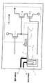
図2は、図1に示したCMOSセンサーの平面図であり、CMOSセンサーの画素部のフォトダイオード周りに、上記埋め込みポリシリコン電極11に負電圧を印加する機構(配線)が形成されている。すなわち、埋め込みポリシリコン電極11の印加電圧を制御するための電極制御配線(破線)40が配設され、また、ホール蓄積層3の印加電圧を制御するための電極制御配線50が配設され、図3のように電極制御配線40は埋め込みポリシリコン電極11に接続され、電極制御配線50はホール蓄積層3に接続されている。 FIG. 2 is a plan view of the CMOS sensor shown in FIG. 1, and a mechanism (wiring) for applying a negative voltage to the buried polysilicon electrode 11 is formed around the photodiode of the pixel portion of the CMOS sensor. That is, an electrode control wiring (broken line) 40 for controlling the applied voltage of the buried polysilicon electrode 11 is disposed, and an
図3は図1に示したCMOSセンサーの配線接続図で、読み出し部N+(FD)7にトランジスタ部のトランジスタTr1のドレイントとトランジスタTr2のゲートが接続され、トランジスタTr1を通してリセット電圧が読み出し部N+(FD)7にパルス的に印加され、また、トランジスタTr2、Tr3により読み出し電圧(光電変換電圧)が増幅され、画素信号が出力されるようになっている。 FIG. 3 is a wiring connection diagram of the CMOS sensor shown in FIG. 1, in which the drain of the transistor Tr1 and the gate of the transistor Tr2 of the transistor unit are connected to the readout unit N + (FD) 7, and the reset voltage is transmitted through the transistor Tr1 to the readout unit N + ( FD) 7 is applied in a pulse manner, and a readout voltage (photoelectric conversion voltage) is amplified by the transistors Tr2 and Tr3 so that a pixel signal is output.
次に本実施の形態の動作について図4、図5を用いて説明する。図4の時刻t0で、CMOSセンサーの受光が開始される。その時、CMOSセンサーの埋め込みポリシリコン電極11には電極制御配線40を介して−3Vが印加されると共に、電極制御配線50を介してホール蓄積層3には正電圧(+1V)が印加される。その時の電位状態は図5(A)に示される。 Next, the operation of this embodiment will be described with reference to FIGS. At time t0 in FIG. 4, light reception by the CMOS sensor is started. At that time, −3 V is applied to the buried polysilicon electrode 11 of the CMOS sensor through the
図4の時刻t0からt1までの受光期間中では、ホール蓄積層3に正電圧(+1V)が継続的に印加される。また、埋め込みポリシリコン電極11に負電圧(−3V)が継続的に印加されることにより、溝10の側面(トレンチ側面)の空乏化を防ぎ、側壁界面からの暗電流抑制を行う。その時の電位状態は図5(B)に示され、信号電荷蓄積N層4に受光量に応じた電荷が蓄積される。なお、図4では、埋め込みポリシリコン電極11の負電圧期間が読み出し期間に入り込んでいるが、これでも支障はない。 A positive voltage (+1 V) is continuously applied to the hole accumulation layer 3 during the light receiving period from time t0 to t1 in FIG. Further, a negative voltage (−3 V) is continuously applied to the buried polysilicon electrode 11 to prevent depletion of the side surface (trench side surface) of the
図4の時刻t1からt1までの読み出し期間では、読み出しゲート6に読み出しパルス(+3V)が印加され、信号電荷蓄積N層4内の信号電荷を読み出してトランジスタ部(図3参照)へ転送する。まず、読み出し期間が開始される時刻t0の直前にリセットゲート8にリセットパルス電圧が印加され、読み出し部N+(FD)7がリセットされる。その後、上記したように時刻t1から時刻t3の間、読み出しゲート6に読み出しパルス電圧(3V)が印加される。時刻t1からt2は読み出し初期期間(前半)で、その時の電位状態は図5(C)に示される。 In the read period from time t1 to time t1 in FIG. 4, a read pulse (+ 3V) is applied to the read
図4の時刻t2からt3までは読み出し期間の後半で、その間はホール蓄積層3の電圧を負電位(−3Vなど)にする。これによって信号電荷蓄積N層4のFD7に対する電位を浅くし、読み出しゲート6との間により大きな電位勾配ができるようにする。この時、ホール蓄積層3がトレンチ側壁P層を通してGndと電気的に接続されるのを防ぐために、埋め込みポリシリコン電極11の印加電圧をー3VからゼロVに戻す制御をして、側壁のピニングをはずす(ホール反転層を無くす)駆動を行う。図5(D)はこの読み出し期間の後半の電位状態図である。その後、時刻t0より受光蓄積期間の開始となり、図5(A)の電位状態に戻る。 From the time t2 to t3 in FIG. 4 is the latter half of the reading period, during which the voltage of the hole accumulation layer 3 is set to a negative potential (such as −3 V). As a result, the potential of the signal charge
本実施形態によれば、CMOSセンサーの画素のトランジスタ分離構造として浅いトレンチ分離を用い、このトレンチ部である溝10をSi酸化膜等の絶縁材で充填し、且つ溝10の内部にポリシリコン電極11を埋め込んだ構造とし、受光期間中には埋め込みポリシリコン電極11を負電圧にすることで、受光部の信号電荷蓄積N層4のトレンチ側壁近傍にホール反転層を誘起し(所謂ピニング状態にする)、トレンチ側壁の界面からの暗電流発生を抑制することができる。 According to this embodiment, shallow trench isolation is used as the transistor isolation structure of the pixel of the CMOS sensor, the
また、受光期間中に受光部上層のホール蓄積層3の電位を正(+1Vなど)にすることにより、受光期間中のP+層と信号電荷蓄積N層4である+Nの間の電界を減少させることができ、この電界の減少により、受光部で発生する白傷等、暗電流の発生を抑制することができる。 Further, the electric field between the P + layer and the signal charge
また、ホール蓄積層3のP+は受光期間中に、受光部が少数キャリアである電子でフルの状態になれば、電子を流すドレインとして機能させることができ、撮像素子のブルーミング抑制機能を持たせることができる。 Further, P + of the hole accumulation layer 3 can function as a drain through which electrons flow when the light receiving portion becomes full of electrons that are minority carriers during the light receiving period, and has a function of suppressing blooming of the image sensor. be able to.
また、受光部ホール蓄積層3に正および負の電圧を印加できる配線50を設けて、受光期間中は正の電圧を印加し、読み出し期間の後半においては負電圧を印加することにより、受光部からの読み出しにポテンシャル差を大きくとれて低電圧の電荷転送を可能にすることができる。 In addition, a
また、本実施の形態では、上記効果により低電圧での受光部からの読み出しが可能なため、センサー部の信号電荷蓄積N層4の濃度を濃く形成してセンサーポテンシャルが深い構造とすることもでき、センサー部の取り扱い電荷量を増大することが可能になる。 Further, in the present embodiment, reading from the light receiving unit at a low voltage is possible due to the above-described effect. Therefore, the signal charge
また、信号電荷を読み出してトランジスタ部へ転送する転送期間内では、上記埋め込みポリシリコン電極11の印加電圧を負電圧から0電圧に制御して側壁のピニングをはずすことによりホール蓄積層3がトレンチ側壁P層を通してGndと電気的に接続されるのを防ぐ駆動を行うことにより取り扱い電荷量を多くできる。 Further, within the transfer period in which the signal charge is read and transferred to the transistor portion, the hole accumulation layer 3 is removed from the trench sidewall by removing the pinning of the sidewall by controlling the applied voltage of the buried polysilicon electrode 11 from the negative voltage to 0 voltage. The amount of charge handled can be increased by driving to prevent electrical connection with Gnd through the P layer.
尚、本発明は上記実施の形態に限定されることなく、その要旨を逸脱しない範囲において、具体的な構成、機能、作用、効果において、他の種々の形態によっても実施することができる。上記実施の形態ではCMOSセンサーに本発明を適用した例について説明しているが、本発明をCCD撮像素子などのその他の撮像素子に適用しても同様の効果を得ることができる。 In addition, this invention is not limited to the said embodiment, In the range which does not deviate from the summary, it can implement also with another various form in a concrete structure, a function, an effect | action, and an effect. In the above embodiment, an example in which the present invention is applied to a CMOS sensor has been described. However, the same effect can be obtained even if the present invention is applied to another image sensor such as a CCD image sensor.
1……基板、2……画素領域Pウエル、3……ホール蓄積層、4……信号電荷蓄積N層、5……読み出し領域、6……読み出しゲート、7……読み出し部N+(FD)、8……リセットゲート、9……STI側壁P層、10……溝、11……埋め込みポリシリコン電極、12……絶縁膜、40、50……電極制御配線。
DESCRIPTION OF
Claims (10)
Translated fromJapanese前記受光部に蓄積された電荷量を検出して画素信号を出力する信号検出部と、
前記受光部の信号電荷を前記信号検出部に読み出す読み出し部と、
前記複数の画素の画素間に設けられたトレンチ分離部と、
前記トレンチ分離部の溝内に埋め込まれた埋め込み電極と、
前記埋め込み電極を駆動する駆動制御部とを具備し、
前記駆動制御部は、受光蓄積期間の少なくとも一部において前記埋め込み電極を第1の電位とし、蓄積された電荷を前記読み出し部を介して前記信号検出部に読み出す読み出し期間の少なくとも一部において前記埋め込み電極を第2の電位とすることを特徴とする撮像装置。A plurality of pixels including a light receiving unit that receives light and generates charges;
A signal detection unit that detects a charge amount accumulated in the light receiving unit and outputs a pixel signal;
A readout unit that reads out the signal charge of the light receiving unit to the signal detection unit;
A trench isolation portion provided between pixels of the plurality of pixels;
Embedded electrodes embedded in the trench isolation trench,
A drive control unit for driving the embedded electrode,
The drive control unit sets the embedded electrode to a first potential in at least a part of a light receiving and accumulating period, and performs the embedding in at least a part of a reading period of reading accumulated charges to the signal detecting unit through the reading unit. An imaging apparatus, wherein an electrode is set to a second potential.
前記トレンチ分離部溝内に電極を埋め込み、受光蓄積期間の少なくとも一部において前記埋め込み電極を第1の電位とし、蓄積された電荷を前記読み出し部を介して前記信号検出部に読み出す読み出し期間の少なくとも一部において前記埋め込み電極を第2の電位とすることを特徴とする駆動制御方法。A plurality of pixels including a light receiving portion that receives light and generates charges, a signal detection portion that detects a charge amount accumulated in the light receiving portion and outputs a pixel signal, and a signal charge of the light receiving portion as the signal detection portion A readout section, a trench isolation section provided between the pixels of the plurality of pixels, a buried electrode embedded in a groove of the trench isolation section, and a drive control section for driving the buried electrode. A drive control method for an imaging apparatus,
An electrode is embedded in the trench isolation part groove, the embedded electrode is set to a first potential in at least a part of a light receiving and accumulating period, and at least a reading period of reading accumulated charge to the signal detecting unit through the reading unit A drive control method characterized in that, in part, the embedded electrode is set to a second potential.
In the entire period of the light receiving and accumulation period and in the first half of the readout period, control is performed such that the upper layer forming the charge generation unit is set to the third potential, and the second half of the readout period is set to the fourth potential. The drive control method according to claim 9.
Priority Applications (1)
| Application Number | Priority Date | Filing Date | Title |
|---|---|---|---|
| JP2004306144AJP4774714B2 (en) | 2004-10-20 | 2004-10-20 | IMAGING DEVICE AND IMAGING DEVICE DRIVE CONTROL METHOD |
Applications Claiming Priority (1)
| Application Number | Priority Date | Filing Date | Title |
|---|---|---|---|
| JP2004306144AJP4774714B2 (en) | 2004-10-20 | 2004-10-20 | IMAGING DEVICE AND IMAGING DEVICE DRIVE CONTROL METHOD |
Publications (2)
| Publication Number | Publication Date |
|---|---|
| JP2006120804Atrue JP2006120804A (en) | 2006-05-11 |
| JP4774714B2 JP4774714B2 (en) | 2011-09-14 |
Family
ID=36538414
Family Applications (1)
| Application Number | Title | Priority Date | Filing Date |
|---|---|---|---|
| JP2004306144AExpired - Fee RelatedJP4774714B2 (en) | 2004-10-20 | 2004-10-20 | IMAGING DEVICE AND IMAGING DEVICE DRIVE CONTROL METHOD |
Country Status (1)
| Country | Link |
|---|---|
| JP (1) | JP4774714B2 (en) |
Cited By (9)
| Publication number | Priority date | Publication date | Assignee | Title |
|---|---|---|---|---|
| JP2011108839A (en)* | 2009-11-17 | 2011-06-02 | Sony Corp | Solid-state imaging device, manufacturing method thereof, and camera |
| CN102132410A (en)* | 2008-08-20 | 2011-07-20 | 科洛司科技有限公司 | Pixel of image sensor with electrically controllable pinning layer |
| JP2012114479A (en)* | 2012-03-19 | 2012-06-14 | Toshiba Corp | Solid state image pickup device |
| US8445950B2 (en) | 2009-12-28 | 2013-05-21 | Kabushiki Kaisha Toshiba | Solid-state imaging device |
| US8872953B2 (en) | 2009-10-30 | 2014-10-28 | Sony Corporation | Solid-state imaging device, manufacturing method thereof, camera, and electronic device |
| CN104377211A (en)* | 2013-08-15 | 2015-02-25 | 全视科技有限公司 | Image sensor pixel cell with switched deep trench isolation structure |
| US9064762B2 (en) | 2008-11-21 | 2015-06-23 | Sony Corporation | Solid-state imaging device, method for manufacturing solid-state imaging device, and imaging apparatus |
| CN114335033A (en)* | 2020-09-30 | 2022-04-12 | 思特威(上海)电子科技股份有限公司 | Ranging pixel structure and TOF image sensor |
| KR20230092888A (en) | 2020-10-29 | 2023-06-26 | 소니 세미컨덕터 솔루션즈 가부시키가이샤 | Solid-state imaging device, manufacturing method therefor, and electronic device |
Citations (3)
| Publication number | Priority date | Publication date | Assignee | Title |
|---|---|---|---|---|
| JPH03273679A (en)* | 1990-03-23 | 1991-12-04 | Matsushita Electron Corp | Solid-state image sensing device |
| JPH04274367A (en)* | 1991-03-01 | 1992-09-30 | Hitachi Ltd | Solid-state image sensing device |
| JP2003234496A (en)* | 2002-02-12 | 2003-08-22 | Sony Corp | Solid-state image pickup device and its manufacturing method |
- 2004
- 2004-10-20JPJP2004306144Apatent/JP4774714B2/ennot_activeExpired - Fee Related
Patent Citations (3)
| Publication number | Priority date | Publication date | Assignee | Title |
|---|---|---|---|---|
| JPH03273679A (en)* | 1990-03-23 | 1991-12-04 | Matsushita Electron Corp | Solid-state image sensing device |
| JPH04274367A (en)* | 1991-03-01 | 1992-09-30 | Hitachi Ltd | Solid-state image sensing device |
| JP2003234496A (en)* | 2002-02-12 | 2003-08-22 | Sony Corp | Solid-state image pickup device and its manufacturing method |
Cited By (15)
| Publication number | Priority date | Publication date | Assignee | Title |
|---|---|---|---|---|
| CN102132410A (en)* | 2008-08-20 | 2011-07-20 | 科洛司科技有限公司 | Pixel of image sensor with electrically controllable pinning layer |
| JP2012500491A (en)* | 2008-08-20 | 2012-01-05 | クロステック・キャピタル,リミテッド・ライアビリティ・カンパニー | Image sensor pixel having an electrically controllable pinning layer |
| JP2013138215A (en)* | 2008-08-20 | 2013-07-11 | Intellectual Venturesii Llc | Pixel of image sensor having electrically controllable pinning layer |
| US8569672B2 (en) | 2008-08-20 | 2013-10-29 | Intellectual Ventures Ii Llc | Pixel of image sensor having electrically controllable pinning layer |
| EP2323165A4 (en)* | 2008-08-20 | 2013-12-25 | Intellectual Ventures Ii Llc | PICTURE SENSOR PIXEL WITH ELECTRICALLY CONTROLLABLE PINNING LAYER |
| US9064762B2 (en) | 2008-11-21 | 2015-06-23 | Sony Corporation | Solid-state imaging device, method for manufacturing solid-state imaging device, and imaging apparatus |
| US8872953B2 (en) | 2009-10-30 | 2014-10-28 | Sony Corporation | Solid-state imaging device, manufacturing method thereof, camera, and electronic device |
| JP2011108839A (en)* | 2009-11-17 | 2011-06-02 | Sony Corp | Solid-state imaging device, manufacturing method thereof, and camera |
| US8445950B2 (en) | 2009-12-28 | 2013-05-21 | Kabushiki Kaisha Toshiba | Solid-state imaging device |
| JP2012114479A (en)* | 2012-03-19 | 2012-06-14 | Toshiba Corp | Solid state image pickup device |
| CN104377211A (en)* | 2013-08-15 | 2015-02-25 | 全视科技有限公司 | Image sensor pixel cell with switched deep trench isolation structure |
| CN104377211B (en)* | 2013-08-15 | 2017-05-31 | 豪威科技股份有限公司 | Image sensor pixel cells with suitching type deep trench isolation structure |
| CN114335033A (en)* | 2020-09-30 | 2022-04-12 | 思特威(上海)电子科技股份有限公司 | Ranging pixel structure and TOF image sensor |
| KR20230092888A (en) | 2020-10-29 | 2023-06-26 | 소니 세미컨덕터 솔루션즈 가부시키가이샤 | Solid-state imaging device, manufacturing method therefor, and electronic device |
| DE112021005749T5 (en) | 2020-10-29 | 2023-08-31 | Sony Semiconductor Solutions Corporation | SOLID STATE IMAGING DEVICE AND MANUFACTURING METHOD THEREOF AND ELECTRONIC DEVICE |
Also Published As
| Publication number | Publication date |
|---|---|
| JP4774714B2 (en) | 2011-09-14 |
Similar Documents
| Publication | Publication Date | Title |
|---|---|---|
| JP4514188B2 (en) | Photoelectric conversion device and imaging device | |
| JP4224036B2 (en) | Image sensor with embedded photodiode region and method of manufacturing the same | |
| JP5335271B2 (en) | Photoelectric conversion device and imaging system using the same | |
| US7217961B2 (en) | Solid-state image pickup device and method for producing the same | |
| US7456888B2 (en) | Photoelectric conversion device and image pick-up system using the photoelectric conversion device | |
| CN1832188B (en) | Solid-state imaging device | |
| KR101272423B1 (en) | Image sensing device and camera | |
| JP5215963B2 (en) | Solid-state imaging device and driving method thereof, manufacturing method of solid-state imaging device, and electronic information device | |
| CN101142681A (en) | Image sensor with embedded photodiode region and method of manufacturing the same | |
| JP2003258232A (en) | Solid-state imaging device | |
| KR101103179B1 (en) | Solid-state imaging device | |
| JP2004055590A (en) | Solid-state imaging device | |
| CN101826539B (en) | Solid-state image capturing device, method of manufacturing solid-state image capturing device, and image capturing apparatus | |
| JP2003234496A (en) | Solid-state image pickup device and its manufacturing method | |
| JP4774714B2 (en) | IMAGING DEVICE AND IMAGING DEVICE DRIVE CONTROL METHOD | |
| JP4241527B2 (en) | Photoelectric conversion element | |
| CN101211840A (en) | CMOS image sensor and manufacturing method thereof | |
| JP2005101864A (en) | Drive method of solid-state image pickup element and solid-state imaging device | |
| JP2002124657A (en) | Cmos image sensor | |
| JP4907941B2 (en) | Solid-state imaging device and driving method thereof | |
| WO2022158236A1 (en) | Light detection device and electronic apparatus | |
| JP2007526638A (en) | Low dark current CMOS image sensor pixel | |
| JP2005311496A (en) | Solid-state imaging apparatus | |
| JP2012084748A (en) | Solid state image sensor and electronic information apparatus | |
| JP2008130795A (en) | Semiconductor device |
Legal Events
| Date | Code | Title | Description |
|---|---|---|---|
| A621 | Written request for application examination | Free format text:JAPANESE INTERMEDIATE CODE: A621 Effective date:20070810 | |
| RD02 | Notification of acceptance of power of attorney | Free format text:JAPANESE INTERMEDIATE CODE: A7422 Effective date:20090817 | |
| RD04 | Notification of resignation of power of attorney | Free format text:JAPANESE INTERMEDIATE CODE: A7424 Effective date:20091013 | |
| A977 | Report on retrieval | Free format text:JAPANESE INTERMEDIATE CODE: A971007 Effective date:20100609 | |
| A131 | Notification of reasons for refusal | Free format text:JAPANESE INTERMEDIATE CODE: A131 Effective date:20100803 | |
| A521 | Request for written amendment filed | Free format text:JAPANESE INTERMEDIATE CODE: A523 Effective date:20100922 | |
| A131 | Notification of reasons for refusal | Free format text:JAPANESE INTERMEDIATE CODE: A131 Effective date:20110308 | |
| A521 | Request for written amendment filed | Free format text:JAPANESE INTERMEDIATE CODE: A523 Effective date:20110509 | |
| TRDD | Decision of grant or rejection written | ||
| A01 | Written decision to grant a patent or to grant a registration (utility model) | Free format text:JAPANESE INTERMEDIATE CODE: A01 Effective date:20110531 | |
| A01 | Written decision to grant a patent or to grant a registration (utility model) | Free format text:JAPANESE INTERMEDIATE CODE: A01 | |
| A61 | First payment of annual fees (during grant procedure) | Free format text:JAPANESE INTERMEDIATE CODE: A61 Effective date:20110613 | |
| FPAY | Renewal fee payment (event date is renewal date of database) | Free format text:PAYMENT UNTIL: 20140708 Year of fee payment:3 | |
| R250 | Receipt of annual fees | Free format text:JAPANESE INTERMEDIATE CODE: R250 | |
| LAPS | Cancellation because of no payment of annual fees |