JP2006114550A - Semiconductor device and its manufacturing method - Google Patents
Semiconductor device and its manufacturing methodDownload PDFInfo
- Publication number
- JP2006114550A JP2006114550AJP2004297652AJP2004297652AJP2006114550AJP 2006114550 AJP2006114550 AJP 2006114550AJP 2004297652 AJP2004297652 AJP 2004297652AJP 2004297652 AJP2004297652 AJP 2004297652AJP 2006114550 AJP2006114550 AJP 2006114550A
- Authority
- JP
- Japan
- Prior art keywords
- insulating film
- gate electrode
- contact plug
- opening
- semiconductor device
- Prior art date
- Legal status (The legal status is an assumption and is not a legal conclusion. Google has not performed a legal analysis and makes no representation as to the accuracy of the status listed.)
- Pending
Links
- 239000004065semiconductorSubstances0.000titleclaimsabstractdescription61
- 238000004519manufacturing processMethods0.000titleclaimsabstractdescription15
- 239000000758substrateSubstances0.000claimsabstractdescription33
- 229910052581Si3N4Inorganic materials0.000claimsabstractdescription17
- HQVNEWCFYHHQES-UHFFFAOYSA-Nsilicon nitrideChemical compoundN12[Si]34N5[Si]62N3[Si]51N64HQVNEWCFYHHQES-UHFFFAOYSA-N0.000claimsabstractdescription17
- 238000000034methodMethods0.000claimsabstractdescription13
- 238000009792diffusion processMethods0.000claimsdescription32
- 238000005530etchingMethods0.000claimsdescription13
- 239000004020conductorSubstances0.000claimsdescription10
- VYPSYNLAJGMNEJ-UHFFFAOYSA-NSilicium dioxideChemical compoundO=[Si]=OVYPSYNLAJGMNEJ-UHFFFAOYSA-N0.000claimsdescription6
- 238000005498polishingMethods0.000claimsdescription6
- 229910052814silicon oxideInorganic materials0.000claimsdescription6
- 239000000126substanceSubstances0.000claimsdescription3
- 238000010030laminatingMethods0.000claimsdescription2
- 239000010410layerSubstances0.000abstractdescription44
- 239000011229interlayerSubstances0.000abstractdescription28
- 230000002950deficientEffects0.000abstractdescription3
- 238000002955isolationMethods0.000description7
- 230000007547defectEffects0.000description4
- 229910052751metalInorganic materials0.000description4
- 239000002184metalSubstances0.000description4
- 229910021332silicideInorganic materials0.000description4
- FVBUAEGBCNSCDD-UHFFFAOYSA-Nsilicide(4-)Chemical compound[Si-4]FVBUAEGBCNSCDD-UHFFFAOYSA-N0.000description4
- WFKWXMTUELFFGS-UHFFFAOYSA-NtungstenChemical compound[W]WFKWXMTUELFFGS-UHFFFAOYSA-N0.000description3
- 229910052721tungstenInorganic materials0.000description3
- 239000010937tungstenSubstances0.000description3
- XUIMIQQOPSSXEZ-UHFFFAOYSA-NSiliconChemical compound[Si]XUIMIQQOPSSXEZ-UHFFFAOYSA-N0.000description2
- 239000000463materialSubstances0.000description2
- 238000000206photolithographyMethods0.000description2
- 229910021420polycrystalline siliconInorganic materials0.000description2
- 229920005591polysiliconPolymers0.000description2
- 229910052710siliconInorganic materials0.000description2
- 239000010703siliconSubstances0.000description2
- 125000006850spacer groupChemical group0.000description2
- 229910004298SiO 2Inorganic materials0.000description1
- 230000015556catabolic processEffects0.000description1
- 230000000052comparative effectEffects0.000description1
- 238000007796conventional methodMethods0.000description1
- 230000000694effectsEffects0.000description1
- 238000005516engineering processMethods0.000description1
- 238000009413insulationMethods0.000description1
- 230000010354integrationEffects0.000description1
- WQJQOUPTWCFRMM-UHFFFAOYSA-Ntungsten disilicideChemical compound[Si]#[W]#[Si]WQJQOUPTWCFRMM-UHFFFAOYSA-N0.000description1
- 229910021342tungsten silicideInorganic materials0.000description1
Images


Classifications
- H—ELECTRICITY
- H01—ELECTRIC ELEMENTS
- H01L—SEMICONDUCTOR DEVICES NOT COVERED BY CLASS H10
- H01L21/00—Processes or apparatus adapted for the manufacture or treatment of semiconductor or solid state devices or of parts thereof
- H01L21/70—Manufacture or treatment of devices consisting of a plurality of solid state components formed in or on a common substrate or of parts thereof; Manufacture of integrated circuit devices or of parts thereof
- H01L21/71—Manufacture of specific parts of devices defined in group H01L21/70
- H01L21/768—Applying interconnections to be used for carrying current between separate components within a device comprising conductors and dielectrics
- H01L21/76897—Formation of self-aligned vias or contact plugs, i.e. involving a lithographically uncritical step
- H—ELECTRICITY
- H10—SEMICONDUCTOR DEVICES; ELECTRIC SOLID-STATE DEVICES NOT OTHERWISE PROVIDED FOR
- H10B—ELECTRONIC MEMORY DEVICES
- H10B41/00—Electrically erasable-and-programmable ROM [EEPROM] devices comprising floating gates
- H10B41/30—Electrically erasable-and-programmable ROM [EEPROM] devices comprising floating gates characterised by the memory core region
- H—ELECTRICITY
- H10—SEMICONDUCTOR DEVICES; ELECTRIC SOLID-STATE DEVICES NOT OTHERWISE PROVIDED FOR
- H10B—ELECTRONIC MEMORY DEVICES
- H10B69/00—Erasable-and-programmable ROM [EPROM] devices not provided for in groups H10B41/00 - H10B63/00, e.g. ultraviolet erasable-and-programmable ROM [UVEPROM] devices
- H—ELECTRICITY
- H01—ELECTRIC ELEMENTS
- H01L—SEMICONDUCTOR DEVICES NOT COVERED BY CLASS H10
- H01L23/00—Details of semiconductor or other solid state devices
- H01L23/48—Arrangements for conducting electric current to or from the solid state body in operation, e.g. leads, terminal arrangements ; Selection of materials therefor
- H01L23/482—Arrangements for conducting electric current to or from the solid state body in operation, e.g. leads, terminal arrangements ; Selection of materials therefor consisting of lead-in layers inseparably applied to the semiconductor body (electrodes)
- H01L23/485—Arrangements for conducting electric current to or from the solid state body in operation, e.g. leads, terminal arrangements ; Selection of materials therefor consisting of lead-in layers inseparably applied to the semiconductor body (electrodes) consisting of layered constructions comprising conductive layers and insulating layers, e.g. planar contacts
- H—ELECTRICITY
- H01—ELECTRIC ELEMENTS
- H01L—SEMICONDUCTOR DEVICES NOT COVERED BY CLASS H10
- H01L2924/00—Indexing scheme for arrangements or methods for connecting or disconnecting semiconductor or solid-state bodies as covered by H01L24/00
- H01L2924/0001—Technical content checked by a classifier
- H01L2924/0002—Not covered by any one of groups H01L24/00, H01L24/00 and H01L2224/00
Landscapes
- Engineering & Computer Science (AREA)
- Physics & Mathematics (AREA)
- Condensed Matter Physics & Semiconductors (AREA)
- General Physics & Mathematics (AREA)
- Manufacturing & Machinery (AREA)
- Computer Hardware Design (AREA)
- Microelectronics & Electronic Packaging (AREA)
- Power Engineering (AREA)
- Internal Circuitry In Semiconductor Integrated Circuit Devices (AREA)
- Semiconductor Memories (AREA)
- Non-Volatile Memory (AREA)
Abstract
Description
Translated fromJapanese本発明は、半導体装置およびその製造方法に関し、より詳しくは、集積度の高い半導体装置およびその製造方法に関する。 The present invention relates to a semiconductor device and a manufacturing method thereof, and more particularly to a highly integrated semiconductor device and a manufacturing method thereof.
近年、半導体装置の集積度の増加に伴い個々の素子の寸法は微小化が進み、各素子を構成する半導体領域の寸法も微細化されている。そして、各半導体領域に接続する配線を埋め込むために絶縁膜に形成するコンタクトホールも微細化され、そのアスペクト比も高くなる傾向にある。 In recent years, with the increase in the degree of integration of semiconductor devices, the dimensions of individual elements have progressed, and the dimensions of semiconductor regions constituting each element have also been reduced. Then, contact holes formed in the insulating film in order to embed wirings connected to the respective semiconductor regions are also miniaturized, and the aspect ratio tends to increase.
コンタクトホールの形成は、従来より、フォトリソグラフィ法を用いて層間絶縁膜を異方性エッチングすることにより行われてきた(例えば、特許文献1および2参照。)。 Conventionally, contact holes have been formed by anisotropic etching of an interlayer insulating film using a photolithography method (see, for example,
例えば、セルフアラインコンタクト(Self Aligned Contact,以下、SACという。)技術によれば、各ゲート電極の上面をシリコン窒化膜で覆い、ゲート電極の両側にシリコン窒化膜スペーサを形成して、コンタクトが形成される部分を予め限定する。その後、シリコン酸化膜からなる層間絶縁膜を形成し、この層間絶縁膜を異方性エッチングすることによってコンタクトホールを形成する。 For example, according to a self-aligned contact (hereinafter referred to as SAC) technique, the upper surface of each gate electrode is covered with a silicon nitride film, and silicon nitride film spacers are formed on both sides of the gate electrode to form a contact. The part to be performed is limited in advance. Thereafter, an interlayer insulating film made of a silicon oxide film is formed, and the interlayer insulating film is anisotropically etched to form a contact hole.
しかしながら、従来のコンタクトホールの形成方法によれば、ホールの側壁は、垂直方向に対して所定のテーパ角を持って形成される。すなわち、底部に行くほどホールの径が縮小するような形状に形成されるので、コンタクトプラグがシリコン基板と接触する部分の面積は小さいものとなる。このため、アスペクト比が高くなると、開口途中でエッチングがストップしてしまい、所望のコンタクトホールを形成できなくなるという問題があった。 However, according to the conventional method for forming a contact hole, the side wall of the hole is formed with a predetermined taper angle with respect to the vertical direction. That is, since the hole diameter is reduced toward the bottom, the area where the contact plug contacts the silicon substrate is small. For this reason, when the aspect ratio becomes high, there is a problem that etching stops in the middle of opening and a desired contact hole cannot be formed.
こうした問題に対しては、コンタクトホールの径を拡大することや、テーパ角を大きくすることによって対処することが考えられる。しかしながら、前者の方法では、狭いピッチでコンタクトホールが配設されるレイアウトの場合に、隣接するコンタクト間で短絡が生じるおそれがある。一方、後者の方法の場合、ホールの側壁を垂直に(すなわち、90度のテーパ角で)形成するのは困難である。特に、SAC技術を用いた場合には、ゲート電極の側壁部上部付近においてゲート−コンタクト間で短絡が起こる原因となる。 It is conceivable to cope with such a problem by increasing the diameter of the contact hole or increasing the taper angle. However, in the former method, in the case of a layout in which contact holes are arranged at a narrow pitch, there is a possibility that a short circuit occurs between adjacent contacts. On the other hand, in the latter method, it is difficult to form the side wall of the hole vertically (that is, with a taper angle of 90 degrees). In particular, when the SAC technique is used, a short circuit occurs between the gate and the contact near the upper portion of the side wall of the gate electrode.
本発明はこのような問題点に鑑みてなされたものである。即ち、本発明の目的は、コンタクトホールの開口不良を改善することのできる半導体装置の製造方法およびこの方法によって形成される半導体装置を提供することにある。 The present invention has been made in view of such problems. That is, an object of the present invention is to provide a method of manufacturing a semiconductor device capable of improving the contact hole opening defect and a semiconductor device formed by this method.
本発明の他の目的および利点は、以下の記載から明らかとなるであろう。 Other objects and advantages of the present invention will become apparent from the following description.
本発明の半導体装置は、半導体基板に形成された拡散層領域と、この半導体基板の上に形成されたゲート絶縁膜と、このゲート絶縁膜の上に形成されたゲート電極と、このゲート電極を被覆する第1の絶縁膜と、この第1の絶縁膜を介しゲート電極の少なくとも一部を被覆するようにして半導体基板の上に形成された第2の絶縁膜と、この第2の絶縁膜の中に形成されて拡散層領域に接続するコンタクトプラグとを有し、このコンタクトプラグが、ゲート電極の幅方向に所定の間隔をおいて並列したストライプ形状を有しており、このストライプ形状がゲート電極によって分断されていることを特徴とするものである。 A semiconductor device according to the present invention includes a diffusion layer region formed on a semiconductor substrate, a gate insulating film formed on the semiconductor substrate, a gate electrode formed on the gate insulating film, and the gate electrode. A first insulating film to be coated; a second insulating film formed on the semiconductor substrate so as to cover at least part of the gate electrode through the first insulating film; and the second insulating film A contact plug formed in the gate electrode and connected to the diffusion layer region, and the contact plug has a stripe shape arranged in parallel at a predetermined interval in the width direction of the gate electrode. It is characterized by being divided by the gate electrode.
また、本発明の半導体装置の製造方法は、半導体基板の上にゲート絶縁膜を形成する工程と、このゲート絶縁膜の上にゲート電極を形成する工程と、このゲート電極を被覆する第1の絶縁膜を形成する工程と、半導体基板にソース拡散層領域およびドレイン拡散層領域を形成する工程と、半導体基板の上に、第1の絶縁膜が形成されたゲート電極を埋め込むようにして第2の絶縁膜を形成する工程と、この第2の絶縁膜をエッチングし、ソース拡散層領域およびドレイン拡散層領域に至り且つゲート電極の幅方向にゲート電極によって分断されるストライプ形状の第1の開口部を形成する工程と、この第1の開口部の内部に導電性材料を埋め込んでコンタクトプラグを形成する工程と、化学的機械研磨法により、第1の絶縁膜が露出するまで第2の絶縁膜および導電性材料を研磨する工程とを有することを特徴とするものである。 The method for manufacturing a semiconductor device according to the present invention includes a step of forming a gate insulating film on a semiconductor substrate, a step of forming a gate electrode on the gate insulating film, and a first covering the gate electrode. A step of forming an insulating film, a step of forming a source diffusion layer region and a drain diffusion layer region on the semiconductor substrate, and a second electrode so as to embed a gate electrode on which the first insulating film is formed on the semiconductor substrate. Forming the first insulating film, and etching the second insulating film to reach the source diffusion layer region and the drain diffusion layer region, and to form a stripe-shaped first opening divided by the gate electrode in the width direction of the gate electrode Forming a contact plug, forming a contact plug by embedding a conductive material in the first opening, and until the first insulating film is exposed by chemical mechanical polishing. It is characterized in that a step of polishing the second insulating film and the conductive material.
この発明は以上説明したように、コンタクトプラグが、ゲート電極の幅方向に所定の間隔をおいて並列したストライプ形状を有しており、また、このストライプ形状がゲート電極によって分断されているので、コンタクトプラグが半導体基板に接触する部分の面積を従来より大きくすることができる。したがって、アスペクト比が高いパターンであっても、コンタクトホールの形成時に開口不良が起こるのを防ぐことが可能となる。 In the present invention, as described above, the contact plug has a stripe shape arranged in parallel at a predetermined interval in the width direction of the gate electrode, and the stripe shape is divided by the gate electrode. The area of the portion where the contact plug contacts the semiconductor substrate can be made larger than before. Therefore, even when the pattern has a high aspect ratio, it is possible to prevent an opening defect from occurring when the contact hole is formed.
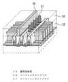
図1は、本発明による半導体装置の斜視図であり、不揮発性メモリの一例としてフラッシュメモリを示している。尚、理解を容易にするために、半導体基板および層間絶縁膜についてはそれぞれ輪郭のみを表している。 FIG. 1 is a perspective view of a semiconductor device according to the present invention, and shows a flash memory as an example of a nonvolatile memory. For ease of understanding, only the contours of the semiconductor substrate and the interlayer insulating film are shown.
図1において、半導体基板(図の破線部)1には、素子分離領域2がストライプ状に配設されている。また、半導体基板1の主面1a上で素子分離領域2と直交する方向には、ゲート絶縁膜3を介して複数のゲート電極4が設けられている。 In FIG. 1,
ゲート電極4は、第1の電極層からなる浮遊ゲート電極層5と、浮遊ゲート電極層5の上に形成された電極間絶縁膜6と、電極間絶縁膜6の上に形成された第2の電極層からなる制御ゲート電極層7とを備え、さらに制御ゲート電極層7の上に金属シリサイド層8が形成された構造を有している。 The
また、ゲート電極4の両側にはソース拡散層領域9およびドレイン拡散層領域10が形成されている。そして、ゲート電極4の上面および側面には、第1の絶縁膜としてのシリコン窒化膜11が形成されている。 A source
半導体基板1の上には、シリコン窒化膜11を介しゲート電極4の少なくとも一部(図では、ゲート電極4の上面を除いた部分)を被覆するようにして、第2の絶縁膜としての層間絶縁膜(図の点線部)12が形成されている。そして、層間絶縁膜12の中には、ソース拡散層領域9およびドレイン拡散層領域10に接続するコンタクトプラグ13が設けられている。 An interlayer as a second insulating film is formed on the
本発明においては、コンタクトプラグ13が、ゲート電極4の幅方向(図の横方向)に所定の間隔をおいて並列したストライプ形状を有しており、このストライプ形状がゲート電極4によって分断されていることを特徴としている。このようにすることによって、コンタクトプラグ13が半導体基板1に接触する部分の面積を従来より大きくすることができる。したがって、アスペクト比が高いパターンであっても、コンタクトホールの形成時に開口不良が起こるのを防ぐことが可能となる。また、ゲート電極との耐圧を確保できるという効果も得られる。 In the present invention, the
比較のために、SAC技術により形成された従来の半導体装置の斜視図を図2に示す。但し、理解を容易にするために、半導体基板および層間絶縁膜については省略している。 For comparison, a perspective view of a conventional semiconductor device formed by SAC technology is shown in FIG. However, the semiconductor substrate and the interlayer insulating film are omitted for easy understanding.
図2において、素子分離領域22が形成された半導体基板(図示せず)の上には、図1と同様のゲート絶縁膜23およびゲート電極24が設けられている。尚、25は浮遊ゲート電極層、26は電極間絶縁膜、27は制御ゲート電極層、28は金属シリサイド層である。また、ゲート電極24の上面および側面には、図1と同様にシリコン窒化膜31が形成されている。 In FIG. 2, a gate
また、層間絶縁膜(図示せず)の中に形成された33はドレインコンタクトプラグであり、半導体基板内のドレイン拡散層領域30に接続している。一方、34はソースコンタクトプラグであり、半導体基板内のソース拡散層領域29に接続している。この構造によれば、コンタクトプラグ(33,34)が拡散層領域(29,30)に接触する部分の面積は小さいものとなる。したがって、アスペクト比が高くなると、コンタクトホールの開口途中でエッチングがストップする不良が起こりやすい。 A
一方、本発明によれば、図1に示すように、ソース拡散層領域9およびドレイン拡散層領域10に接続するコンタクトプラグ13をいずれもストライプ状に形成する。したがって、図2のドレインコンタクトプラグ33のように円柱状に形成した場合に比較して、拡散層領域(9,10)との接触面積を大きくすることができる。よって、アスペクト比が高い場合であっても、エッチングの際に開口不良が起こるのを防いで、所望のコンタクトプラグを形成することが可能となる。 On the other hand, according to the present invention, as shown in FIG. 1, the
次に、図3〜図7を用いて、本発明による半導体装置の製造方法について説明する。尚、理解を容易にするために、半導体基板および層間絶縁膜についてはそれぞれ輪郭を破線または点線で表している。 Next, a method for manufacturing a semiconductor device according to the present invention will be described with reference to FIGS. For easy understanding, the outlines of the semiconductor substrate and the interlayer insulating film are indicated by broken lines or dotted lines, respectively.
まず、半導体基板(図の破線部)41に素子分離領域42を形成した後、その主面41a上にゲート絶縁膜43、ゲート電極44およびシリコン窒化膜45を順に形成する(図3)。 First, an
例えば、半導体基板41としてシリコン基板を用い、所定領域にシリコン酸化膜を埋め込むことによって、STI(Shallow Trench Isolation)構造の素子分離領域42を形成する。次に、半導体基板41の上にゲート絶縁膜43を形成してから、ゲート絶縁膜43を介してゲート電極44を形成する。次いで、絶縁のためにゲート電極44の上面および側面をシリコン窒化膜45で覆う。ゲート電極44の側壁部に形成されたシリコン窒化膜45はサイドウォールスペーサである。 For example, a silicon substrate is used as the semiconductor substrate 41, and a silicon oxide film is embedded in a predetermined region, thereby forming an
次いで、ゲート電極44の両側にソース拡散層領域46およびドレイン拡散層領域47を形成する(図3)。 Next, a source
本発明においては、ゲート絶縁膜43やゲート電極44を構成する材料に特に制限はない。例えば、ゲート絶縁膜43として、シリコン酸化膜(SiO2膜)を用いることができる。また、ゲート電極44は、例えば、第1の電極層としてのポリシリコン膜48、電極間絶縁膜としてのシリコン酸化膜49、第2の電極層としてのポリシリコン膜50をこの順に積層した後、さらに、金属シリサイド層としてのタングステンシリサイド層(WSi層)51を設けることによって形成することができる。In the present invention, the material constituting the
また、本発明においては、シリコン窒化膜45以外の他の膜を用いてゲート電極44を覆ってもよい。但し、後述する層間絶縁膜52とのエッチング選択比が大きい材料からなる膜であることを要する。 In the present invention, the
次に、シリコン窒化膜45の形成されたゲート電極44を埋め込むようにして、半導体基板41の上に層間絶縁膜(図3の点線部)52を形成する。本実施の形態においては、シリコン窒化膜45とのエッチング選択比が大きいシリコン酸化膜を層間絶縁膜52として用いることができる。 Next, an interlayer insulating film (dotted line portion in FIG. 3) 52 is formed on the semiconductor substrate 41 so as to bury the
次いで、フォトリソグラフィ法を用いて、層間絶縁膜52の主面52a上に所定のパターンを有するレジスト膜53を形成する(図4)。レジスト膜53のパターンは、ゲート電極44の幅方向に所定の間隔をおいて並列したストライプ形状のパターンであるとする。そして、レジスト膜53をマスクとして層間絶縁膜52をドライエッチングした後、不要となったレジスト膜53を除去する。このとき、層間絶縁膜52のエッチングは、シリコン窒化膜45とのエッチング選択比が大きくなる条件で行う。これにより、ゲート電極44をエッチングすることなしに、ソース拡散層領域46およびドレイン拡散層領域47に至る第1の開口部(図示せず)を層間絶縁膜52に形成することができる。 Next, a resist
次に、第1の開口部の内部にタングステン(W)などの導電性材料を埋め込み、コンタクトプラグ54を形成する。その後、CMP(Chemical Mechanical Polishing)法を用いて、窒化シリコン膜45の表面が露出するまで層間絶縁膜52を研磨する。これにより、図5の構造が得られる。 Next, a conductive material such as tungsten (W) is embedded in the first opening to form a
コンタクトプラグ54から電気的ノードを取り出すためには、図5の構造で層間絶縁膜52の上に、第3の絶縁膜としての層間絶縁膜(図6の点線部)55を形成する。次いで、層間絶縁膜55に、コンタクトプラグ54に至る第2の開口部および第3の開口部(図示せず)を形成する。ここで、第2の開口部は、ソース拡散層領域46に接続するコンタクトプラグ54に至る開口部である。また、第3の開口部は、ドレイン拡散層領域47に接続するコンタクトプラグ54に至る開口部である。ここで、層間絶縁膜55の膜厚は、層間絶縁膜52の膜厚に比較して薄くすることができるので、第2の開口部および第3の開口部の形状はライン状に限らず円筒状であってもよい。続いて、これらの開口部の内部にタングステン(W)などの導電性材料を埋め込み、ソースコンタクトプラグ56およびドレインコンタクトプラグ57を形成する。これにより、図6の構造が得られる。図6では、ソースコンタクトプラグ56がライン状に形成されており、ドレインコンタクトプラグ57が円筒状に形成されている。 In order to take out an electrical node from the
さらに、図6の構造の上に、第4の絶縁膜としての層間絶縁膜(図7の点線部)58を形成する。次いで、層間絶縁膜58に、ドレインコンタクトプラグ57に至る第4の開口部(図示せず)を設ける。第4の開口部の形状は、ドレインコンタクトプラグ57の形状と同じ(すなわち、円筒状)とする。そして、この第4の開口部の内部にタングステン(W)などの導電性材料を埋め込む。これにより、積層されたドレインコンタクトプラグ57´が得られる。その後、ドレインコンタクトプラグ57´に接続するビット線59を形成することによって、図7に示す構造とすることができる。 Further, an interlayer insulating film (dotted line portion in FIG. 7) 58 as a fourth insulating film is formed on the structure of FIG. Next, a fourth opening (not shown) reaching the
尚、層間絶縁膜58に、ソースコンタクトプラグ56に至る開口部を設け、これに導電性材料を埋め込むことによって、積層されたソースコンタクトプラグを形成してもよい。この場合、開口部は、ソースコンタクトプラグ56の形状と同じ(すなわち、ライン状)に形成する。 Note that a stacked source contact plug may be formed by providing an opening reaching the source contact plug 56 in the
また、本実施の形態において開口部を円筒状に形成する場合、その平面形状は円に限らず楕円であってもよい。楕円状に開口することによって、円状に開口した場合に比較して開口不良を一層低減することが可能となる。 Further, when the opening is formed in a cylindrical shape in the present embodiment, the planar shape is not limited to a circle and may be an ellipse. By opening in an elliptical shape, it becomes possible to further reduce defective openings as compared to the case of opening in a circular shape.
1,41 半導体基板
2,22,42 素子分離領域
3,23,43 ゲート絶縁膜
4,24,44 ゲート電極
5,25,48 浮遊ゲート電極層
6,26,49 電極間絶縁膜
7,27,50 制御ゲート電極層
8,28,51 金属シリサイド層
9,29,46 ソース拡散層領域
10,30,47 ドレイン拡散層領域
11,31,45 シリコン窒化膜
12,52,55,58 層間絶縁膜
13,54 コンタクトプラグ
33,57 ドレインコンタクトプラグ
34,56 ソースコンタクトプラグ
53 レジスト膜
59 ビット線1, 41
Claims (8)
Translated fromJapanese前記半導体基板の上に形成されたゲート絶縁膜と、
前記ゲート絶縁膜の上に形成されたゲート電極と、
前記ゲート電極を被覆する第1の絶縁膜と、
前記第1の絶縁膜を介し前記ゲート電極の少なくとも一部を被覆するようにして前記半導体基板の上に形成された第2の絶縁膜と、
前記第2の絶縁膜の中に形成されて前記拡散層領域に接続するコンタクトプラグとを有し、
前記コンタクトプラグは、前記ゲート電極の幅方向に所定の間隔をおいて並列したストライプ形状を有しており、該ストライプ形状が前記ゲート電極によって分断されていることを特徴とする半導体装置。A diffusion layer region formed in a semiconductor substrate;
A gate insulating film formed on the semiconductor substrate;
A gate electrode formed on the gate insulating film;
A first insulating film covering the gate electrode;
A second insulating film formed on the semiconductor substrate so as to cover at least a part of the gate electrode via the first insulating film;
A contact plug formed in the second insulating film and connected to the diffusion layer region;
The semiconductor device according to claim 1, wherein the contact plug has a stripe shape arranged in parallel at a predetermined interval in the width direction of the gate electrode, and the stripe shape is divided by the gate electrode.
前記浮遊ゲート電極層の上に形成された電極間絶縁膜と、
前記電極間絶縁膜の上に形成された第2の電極層からなる制御ゲート電極層とを有する請求項1に記載の半導体装置。The gate electrode includes a floating gate electrode layer made of a first electrode layer;
An interelectrode insulating film formed on the floating gate electrode layer;
The semiconductor device according to claim 1, further comprising: a control gate electrode layer made of a second electrode layer formed on the interelectrode insulating film.
前記ゲート絶縁膜の上にゲート電極を形成する工程と、
前記ゲート電極を被覆する第1の絶縁膜を形成する工程と、
前記半導体基板にソース拡散層領域およびドレイン拡散層領域を形成する工程と、
前記半導体基板の上に、前記第1の絶縁膜が形成された前記ゲート電極を埋め込むようにして第2の絶縁膜を形成する工程と、
前記第2の絶縁膜をエッチングし、前記ソース拡散層領域および前記ドレイン拡散層領域に至り且つ前記ゲート電極の幅方向に前記ゲート電極によって分断されるストライプ形状の第1の開口部を形成する工程と、
前記第1の開口部の内部に導電性材料を埋め込んでコンタクトプラグを形成する工程と、
化学的機械研磨法により、前記第1の絶縁膜が露出するまで前記第2の絶縁膜および前記導電性材料を研磨する工程とを有することを特徴とする半導体装置の製造方法。Forming a gate insulating film on the semiconductor substrate;
Forming a gate electrode on the gate insulating film;
Forming a first insulating film covering the gate electrode;
Forming a source diffusion layer region and a drain diffusion layer region in the semiconductor substrate;
Forming a second insulating film on the semiconductor substrate so as to bury the gate electrode on which the first insulating film is formed;
Etching the second insulating film to form a stripe-shaped first opening that reaches the source diffusion layer region and the drain diffusion layer region and is divided by the gate electrode in the width direction of the gate electrode. When,
Forming a contact plug by embedding a conductive material in the first opening;
And a step of polishing the second insulating film and the conductive material until the first insulating film is exposed by a chemical mechanical polishing method.
前記第3の絶縁膜をエッチングし、前記ソース拡散層領域に接続する前記コンタクトプラグに至る第2の開口部と、前記ドレイン拡散層領域に接続する前記コンタクトプラグに至る第3の開口部とを形成する工程と、
前記第2の開口部および前記第3の開口部に導電性材料を埋め込んで、ソースコンタクトプラグおよびドレインコンタクトプラグを形成する工程と、
前記第3の絶縁膜の上に第4の絶縁膜を形成する工程と、
前記第4の絶縁膜をエッチングし、前記ソースコンタクトプラグおよび前記ドレインコンタクトプラグのいずれか一方に至る第4の開口部を形成する工程と、
前記第4の開口部に導電性材料を埋め込んで、前記ソースコンタクトプラグおよび前記ドレインコンタクトプラグのいずれか一方にさらにコンタクトプラグを積層する工程と、
前記積層したコンタクトプラグに接続する配線層を形成する工程とを有する請求項5に記載の半導体装置の製造方法。Forming a third insulating film on the first insulating film, the second insulating film and the contact plug after finishing the polishing;
Etching the third insulating film to form a second opening reaching the contact plug connected to the source diffusion layer region and a third opening reaching the contact plug connected to the drain diffusion layer region Forming, and
Burying a conductive material in the second opening and the third opening to form a source contact plug and a drain contact plug;
Forming a fourth insulating film on the third insulating film;
Etching the fourth insulating film to form a fourth opening reaching one of the source contact plug and the drain contact plug;
Burying a conductive material in the fourth opening, and further laminating a contact plug on either the source contact plug or the drain contact plug;
6. The method of manufacturing a semiconductor device according to claim 5, further comprising a step of forming a wiring layer connected to the stacked contact plugs.
Priority Applications (2)
| Application Number | Priority Date | Filing Date | Title |
|---|---|---|---|
| JP2004297652AJP2006114550A (en) | 2004-10-12 | 2004-10-12 | Semiconductor device and its manufacturing method |
| US11/245,046US20060081909A1 (en) | 2004-10-12 | 2005-10-07 | Semiconductor device and manufacturing method therefor |
Applications Claiming Priority (1)
| Application Number | Priority Date | Filing Date | Title |
|---|---|---|---|
| JP2004297652AJP2006114550A (en) | 2004-10-12 | 2004-10-12 | Semiconductor device and its manufacturing method |
Publications (1)
| Publication Number | Publication Date |
|---|---|
| JP2006114550Atrue JP2006114550A (en) | 2006-04-27 |
Family
ID=36179836
Family Applications (1)
| Application Number | Title | Priority Date | Filing Date |
|---|---|---|---|
| JP2004297652APendingJP2006114550A (en) | 2004-10-12 | 2004-10-12 | Semiconductor device and its manufacturing method |
Country Status (2)
| Country | Link |
|---|---|
| US (1) | US20060081909A1 (en) |
| JP (1) | JP2006114550A (en) |
Families Citing this family (3)
| Publication number | Priority date | Publication date | Assignee | Title |
|---|---|---|---|---|
| US10672708B2 (en) | 2015-11-30 | 2020-06-02 | Taiwan Semiconductor Manufacturing Co., Ltd. | Standard-cell layout structure with horn power and smart metal cut |
| CN113078165B (en)* | 2020-01-03 | 2023-07-25 | 联华电子股份有限公司 | Non-volatile memory and method of forming same |
| CN113078164B (en)* | 2021-03-26 | 2022-04-15 | 长江存储科技有限责任公司 | a semiconductor device |
Family Cites Families (4)
| Publication number | Priority date | Publication date | Assignee | Title |
|---|---|---|---|---|
| IT1243303B (en)* | 1990-07-24 | 1994-05-26 | Sgs Thomson Microelectronics | DEPLOYING OF MEMORY CELLS WITH METAL LINES OF SOURCE AND DRAIN CONNECTION FORMED ON THE SUBSTRATE AND ORTHOGONALLY OVERLAYED BY LINES OF GATE CONNECTION AND PROCEDURE FOR ITS MANUFACTURE |
| US6008516A (en)* | 1997-07-23 | 1999-12-28 | Texas Instruments Incorporated | Non-volatile flash layout |
| JP4586219B2 (en)* | 1999-09-17 | 2010-11-24 | ソニー株式会社 | Erase method for nonvolatile semiconductor memory device |
| JP2003188252A (en)* | 2001-12-13 | 2003-07-04 | Toshiba Corp | Semiconductor device and manufacturing method thereof |
- 2004
- 2004-10-12JPJP2004297652Apatent/JP2006114550A/enactivePending
- 2005
- 2005-10-07USUS11/245,046patent/US20060081909A1/ennot_activeAbandoned
Also Published As
| Publication number | Publication date |
|---|---|
| US20060081909A1 (en) | 2006-04-20 |
Similar Documents
| Publication | Publication Date | Title |
|---|---|---|
| JP5348372B2 (en) | Semiconductor device, method for manufacturing the same, and method for manufacturing DRAM | |
| JP2006351861A (en) | Manufacturing method of semiconductor device | |
| KR20110028971A (en) | A manufacturing method of a semiconductor device in which two kinds of contact holes of different sizes are formed by one photo process | |
| JP4901898B2 (en) | Manufacturing method of semiconductor device | |
| JP2009044004A (en) | Semiconductor device and manufacturing method thereof | |
| JP2012199381A (en) | Semiconductor device and manufacturing method thereof | |
| JP2013051415A (en) | Semiconductor element and method of manufacturing the same | |
| JP2009152361A (en) | Semiconductor device and manufacturing method thereof | |
| KR100583964B1 (en) | Semiconductor device having raised cell landing pad and manufacturing method thereof | |
| KR100924007B1 (en) | Method of forming vertical channel transistor of semiconductor device | |
| JP2008205379A (en) | Nonvolatile semiconductor memory and manufacturing method thereof | |
| US7615818B2 (en) | Semiconductor device and method of manufacturing the same | |
| KR100827509B1 (en) | Method of forming a semiconductor device | |
| JP2007281200A (en) | Manufacturing method of semiconductor device | |
| KR20110113372A (en) | Semiconductor device and manufacturing method thereof | |
| JP2006114550A (en) | Semiconductor device and its manufacturing method | |
| KR20140028906A (en) | Semiconductor device and method for manufacturing the same | |
| US20070196983A1 (en) | Method of manufacturing non-volatile memory device | |
| JP2010109183A (en) | Semiconductor device and manufacturing method | |
| JP5100981B2 (en) | Landing plug contact hole mask and plug forming method using the same | |
| JP2010080602A (en) | Semiconductor apparatus and method of manufacturing the same | |
| KR101149053B1 (en) | Method of forming a storage node contact of a semiconductor device | |
| JP2008218638A (en) | Semiconductor device and manufacturing method thereof | |
| US20120220115A1 (en) | Method for fabricating semiconductor device | |
| JP2016039303A (en) | Semiconductor device and method of manufacturing the same |