JP2006100752A - Circuit arrangement and its manufacturing method - Google Patents
Circuit arrangement and its manufacturing methodDownload PDFInfo
- Publication number
- JP2006100752A JP2006100752AJP2004288213AJP2004288213AJP2006100752AJP 2006100752 AJP2006100752 AJP 2006100752AJP 2004288213 AJP2004288213 AJP 2004288213AJP 2004288213 AJP2004288213 AJP 2004288213AJP 2006100752 AJP2006100752 AJP 2006100752A
- Authority
- JP
- Japan
- Prior art keywords
- sealing resin
- circuit board
- circuit
- circuit device
- thermal expansion
- Prior art date
- Legal status (The legal status is an assumption and is not a legal conclusion. Google has not performed a legal analysis and makes no representation as to the accuracy of the status listed.)
- Pending
Links
- 238000004519manufacturing processMethods0.000titleclaimsdescription25
- 229920005989resinPolymers0.000claimsabstractdescription116
- 239000011347resinSubstances0.000claimsabstractdescription116
- 238000007789sealingMethods0.000claimsabstractdescription89
- 238000000034methodMethods0.000claimsabstractdescription23
- 229920001187thermosetting polymerPolymers0.000claimsabstractdescription16
- 239000011248coating agentSubstances0.000claimsabstractdescription7
- 238000000576coating methodMethods0.000claimsabstractdescription7
- 239000000758substrateSubstances0.000claimsdescription54
- 239000000945fillerSubstances0.000claimsdescription32
- 229910000679solderInorganic materials0.000claimsdescription20
- 229910052782aluminiumInorganic materials0.000claimsdescription16
- XAGFODPZIPBFFR-UHFFFAOYSA-NaluminiumChemical compound[Al]XAGFODPZIPBFFR-UHFFFAOYSA-N0.000claimsdescription16
- 238000001721transfer mouldingMethods0.000claimsdescription9
- 239000010949copperSubstances0.000claimsdescription8
- RYGMFSIKBFXOCR-UHFFFAOYSA-NCopperChemical compound[Cu]RYGMFSIKBFXOCR-UHFFFAOYSA-N0.000claimsdescription7
- 229910052802copperInorganic materials0.000claimsdescription7
- 238000010438heat treatmentMethods0.000claimsdescription2
- 238000000465mouldingMethods0.000claimsdescription2
- 229910052751metalInorganic materials0.000abstractdescription24
- 239000002184metalSubstances0.000abstractdescription24
- 230000008602contractionEffects0.000abstractdescription12
- 238000001723curingMethods0.000description21
- 239000000463materialSubstances0.000description17
- 239000004065semiconductorSubstances0.000description13
- 230000005855radiationEffects0.000description12
- 230000035882stressEffects0.000description10
- 238000005452bendingMethods0.000description7
- 239000004519greaseSubstances0.000description5
- 230000002093peripheral effectEffects0.000description5
- 238000003825pressingMethods0.000description5
- 239000011888foilSubstances0.000description4
- 230000017525heat dissipationEffects0.000description4
- 238000005520cutting processMethods0.000description3
- 239000012530fluidSubstances0.000description3
- 239000007788liquidSubstances0.000description3
- 239000007787solidSubstances0.000description3
- 230000008646thermal stressEffects0.000description3
- 229910018072Al 2 O 3Inorganic materials0.000description2
- 238000005219brazingMethods0.000description2
- 239000003990capacitorSubstances0.000description2
- 239000000428dustSubstances0.000description2
- 230000005496eutecticsEffects0.000description2
- 238000001039wet etchingMethods0.000description2
- 229910017944Ag—CuInorganic materials0.000description1
- 229910001111Fine metalInorganic materials0.000description1
- 229910020836Sn-AgInorganic materials0.000description1
- 229910020888Sn-CuInorganic materials0.000description1
- 229910020994Sn-ZnInorganic materials0.000description1
- 229910020988Sn—AgInorganic materials0.000description1
- 229910019204Sn—CuInorganic materials0.000description1
- 229910009069Sn—ZnInorganic materials0.000description1
- 230000001154acute effectEffects0.000description1
- 229910052797bismuthInorganic materials0.000description1
- 238000005336crackingMethods0.000description1
- 230000007423decreaseEffects0.000description1
- 239000003822epoxy resinSubstances0.000description1
- 238000005530etchingMethods0.000description1
- 238000002474experimental methodMethods0.000description1
- 238000013007heat curingMethods0.000description1
- 229910052738indiumInorganic materials0.000description1
- 239000011159matrix materialSubstances0.000description1
- 238000010397one-hybrid screeningMethods0.000description1
- TWNQGVIAIRXVLR-UHFFFAOYSA-Noxo(oxoalumanyloxy)alumaneChemical compoundO=[Al]O[Al]=OTWNQGVIAIRXVLR-UHFFFAOYSA-N0.000description1
- 238000000059patterningMethods0.000description1
- 229920000647polyepoxidePolymers0.000description1
- 238000004080punchingMethods0.000description1
- 238000000926separation methodMethods0.000description1
- 238000010008shearingMethods0.000description1
Images


Classifications
- A—HUMAN NECESSITIES
- A47—FURNITURE; DOMESTIC ARTICLES OR APPLIANCES; COFFEE MILLS; SPICE MILLS; SUCTION CLEANERS IN GENERAL
- A47J—KITCHEN EQUIPMENT; COFFEE MILLS; SPICE MILLS; APPARATUS FOR MAKING BEVERAGES
- A47J27/00—Cooking-vessels
- A47J27/02—Cooking-vessels with enlarged heating surfaces
- H—ELECTRICITY
- H01—ELECTRIC ELEMENTS
- H01L—SEMICONDUCTOR DEVICES NOT COVERED BY CLASS H10
- H01L21/00—Processes or apparatus adapted for the manufacture or treatment of semiconductor or solid state devices or of parts thereof
- H01L21/02—Manufacture or treatment of semiconductor devices or of parts thereof
- H01L21/04—Manufacture or treatment of semiconductor devices or of parts thereof the devices having potential barriers, e.g. a PN junction, depletion layer or carrier concentration layer
- H01L21/50—Assembly of semiconductor devices using processes or apparatus not provided for in a single one of the groups H01L21/18 - H01L21/326 or H10D48/04 - H10D48/07 e.g. sealing of a cap to a base of a container
- H01L21/56—Encapsulations, e.g. encapsulation layers, coatings
- H01L21/565—Moulds
- H—ELECTRICITY
- H01—ELECTRIC ELEMENTS
- H01L—SEMICONDUCTOR DEVICES NOT COVERED BY CLASS H10
- H01L23/00—Details of semiconductor or other solid state devices
- H01L23/28—Encapsulations, e.g. encapsulating layers, coatings, e.g. for protection
- H01L23/29—Encapsulations, e.g. encapsulating layers, coatings, e.g. for protection characterised by the material, e.g. carbon
- H01L23/293—Organic, e.g. plastic
- H—ELECTRICITY
- H01—ELECTRIC ELEMENTS
- H01L—SEMICONDUCTOR DEVICES NOT COVERED BY CLASS H10
- H01L23/00—Details of semiconductor or other solid state devices
- H01L23/28—Encapsulations, e.g. encapsulating layers, coatings, e.g. for protection
- H01L23/31—Encapsulations, e.g. encapsulating layers, coatings, e.g. for protection characterised by the arrangement or shape
- H01L23/3107—Encapsulations, e.g. encapsulating layers, coatings, e.g. for protection characterised by the arrangement or shape the device being completely enclosed
- H01L23/3121—Encapsulations, e.g. encapsulating layers, coatings, e.g. for protection characterised by the arrangement or shape the device being completely enclosed a substrate forming part of the encapsulation
- H—ELECTRICITY
- H01—ELECTRIC ELEMENTS
- H01L—SEMICONDUCTOR DEVICES NOT COVERED BY CLASS H10
- H01L23/00—Details of semiconductor or other solid state devices
- H01L23/48—Arrangements for conducting electric current to or from the solid state body in operation, e.g. leads, terminal arrangements ; Selection of materials therefor
- H01L23/488—Arrangements for conducting electric current to or from the solid state body in operation, e.g. leads, terminal arrangements ; Selection of materials therefor consisting of soldered or bonded constructions
- H01L23/495—Lead-frames or other flat leads
- H01L23/49517—Additional leads
- H01L23/49531—Additional leads the additional leads being a wiring board
- H—ELECTRICITY
- H01—ELECTRIC ELEMENTS
- H01L—SEMICONDUCTOR DEVICES NOT COVERED BY CLASS H10
- H01L24/00—Arrangements for connecting or disconnecting semiconductor or solid-state bodies; Methods or apparatus related thereto
- H01L24/93—Batch processes
- H01L24/95—Batch processes at chip-level, i.e. with connecting carried out on a plurality of singulated devices, i.e. on diced chips
- H01L24/97—Batch processes at chip-level, i.e. with connecting carried out on a plurality of singulated devices, i.e. on diced chips the devices being connected to a common substrate, e.g. interposer, said common substrate being separable into individual assemblies after connecting
- H—ELECTRICITY
- H05—ELECTRIC TECHNIQUES NOT OTHERWISE PROVIDED FOR
- H05K—PRINTED CIRCUITS; CASINGS OR CONSTRUCTIONAL DETAILS OF ELECTRIC APPARATUS; MANUFACTURE OF ASSEMBLAGES OF ELECTRICAL COMPONENTS
- H05K3/00—Apparatus or processes for manufacturing printed circuits
- H05K3/22—Secondary treatment of printed circuits
- H05K3/28—Applying non-metallic protective coatings
- H05K3/285—Permanent coating compositions
- A—HUMAN NECESSITIES
- A47—FURNITURE; DOMESTIC ARTICLES OR APPLIANCES; COFFEE MILLS; SPICE MILLS; SUCTION CLEANERS IN GENERAL
- A47J—KITCHEN EQUIPMENT; COFFEE MILLS; SPICE MILLS; APPARATUS FOR MAKING BEVERAGES
- A47J27/00—Cooking-vessels
- A47J27/002—Construction of cooking-vessels; Methods or processes of manufacturing specially adapted for cooking-vessels
- A—HUMAN NECESSITIES
- A47—FURNITURE; DOMESTIC ARTICLES OR APPLIANCES; COFFEE MILLS; SPICE MILLS; SUCTION CLEANERS IN GENERAL
- A47J—KITCHEN EQUIPMENT; COFFEE MILLS; SPICE MILLS; APPARATUS FOR MAKING BEVERAGES
- A47J36/00—Parts, details or accessories of cooking-vessels
- A47J36/02—Selection of specific materials, e.g. heavy bottoms with copper inlay or with insulating inlay
- H—ELECTRICITY
- H01—ELECTRIC ELEMENTS
- H01L—SEMICONDUCTOR DEVICES NOT COVERED BY CLASS H10
- H01L2224/00—Indexing scheme for arrangements for connecting or disconnecting semiconductor or solid-state bodies and methods related thereto as covered by H01L24/00
- H01L2224/01—Means for bonding being attached to, or being formed on, the surface to be connected, e.g. chip-to-package, die-attach, "first-level" interconnects; Manufacturing methods related thereto
- H01L2224/42—Wire connectors; Manufacturing methods related thereto
- H01L2224/44—Structure, shape, material or disposition of the wire connectors prior to the connecting process
- H01L2224/45—Structure, shape, material or disposition of the wire connectors prior to the connecting process of an individual wire connector
- H01L2224/45001—Core members of the connector
- H01L2224/45099—Material
- H01L2224/451—Material with a principal constituent of the material being a metal or a metalloid, e.g. boron (B), silicon (Si), germanium (Ge), arsenic (As), antimony (Sb), tellurium (Te) and polonium (Po), and alloys thereof
- H—ELECTRICITY
- H01—ELECTRIC ELEMENTS
- H01L—SEMICONDUCTOR DEVICES NOT COVERED BY CLASS H10
- H01L2224/00—Indexing scheme for arrangements for connecting or disconnecting semiconductor or solid-state bodies and methods related thereto as covered by H01L24/00
- H01L2224/01—Means for bonding being attached to, or being formed on, the surface to be connected, e.g. chip-to-package, die-attach, "first-level" interconnects; Manufacturing methods related thereto
- H01L2224/42—Wire connectors; Manufacturing methods related thereto
- H01L2224/47—Structure, shape, material or disposition of the wire connectors after the connecting process
- H01L2224/48—Structure, shape, material or disposition of the wire connectors after the connecting process of an individual wire connector
- H01L2224/4805—Shape
- H01L2224/4809—Loop shape
- H01L2224/48091—Arched
- H—ELECTRICITY
- H01—ELECTRIC ELEMENTS
- H01L—SEMICONDUCTOR DEVICES NOT COVERED BY CLASS H10
- H01L2224/00—Indexing scheme for arrangements for connecting or disconnecting semiconductor or solid-state bodies and methods related thereto as covered by H01L24/00
- H01L2224/73—Means for bonding being of different types provided for in two or more of groups H01L2224/10, H01L2224/18, H01L2224/26, H01L2224/34, H01L2224/42, H01L2224/50, H01L2224/63, H01L2224/71
- H01L2224/732—Location after the connecting process
- H01L2224/73251—Location after the connecting process on different surfaces
- H01L2224/73265—Layer and wire connectors
- H—ELECTRICITY
- H01—ELECTRIC ELEMENTS
- H01L—SEMICONDUCTOR DEVICES NOT COVERED BY CLASS H10
- H01L2224/00—Indexing scheme for arrangements for connecting or disconnecting semiconductor or solid-state bodies and methods related thereto as covered by H01L24/00
- H01L2224/93—Batch processes
- H01L2224/95—Batch processes at chip-level, i.e. with connecting carried out on a plurality of singulated devices, i.e. on diced chips
- H01L2224/97—Batch processes at chip-level, i.e. with connecting carried out on a plurality of singulated devices, i.e. on diced chips the devices being connected to a common substrate, e.g. interposer, said common substrate being separable into individual assemblies after connecting
- H—ELECTRICITY
- H01—ELECTRIC ELEMENTS
- H01L—SEMICONDUCTOR DEVICES NOT COVERED BY CLASS H10
- H01L23/00—Details of semiconductor or other solid state devices
- H01L23/28—Encapsulations, e.g. encapsulating layers, coatings, e.g. for protection
- H01L23/31—Encapsulations, e.g. encapsulating layers, coatings, e.g. for protection characterised by the arrangement or shape
- H01L23/3107—Encapsulations, e.g. encapsulating layers, coatings, e.g. for protection characterised by the arrangement or shape the device being completely enclosed
- H01L23/3135—Double encapsulation or coating and encapsulation
- H—ELECTRICITY
- H01—ELECTRIC ELEMENTS
- H01L—SEMICONDUCTOR DEVICES NOT COVERED BY CLASS H10
- H01L24/00—Arrangements for connecting or disconnecting semiconductor or solid-state bodies; Methods or apparatus related thereto
- H01L24/01—Means for bonding being attached to, or being formed on, the surface to be connected, e.g. chip-to-package, die-attach, "first-level" interconnects; Manufacturing methods related thereto
- H01L24/42—Wire connectors; Manufacturing methods related thereto
- H01L24/44—Structure, shape, material or disposition of the wire connectors prior to the connecting process
- H01L24/45—Structure, shape, material or disposition of the wire connectors prior to the connecting process of an individual wire connector
- H—ELECTRICITY
- H01—ELECTRIC ELEMENTS
- H01L—SEMICONDUCTOR DEVICES NOT COVERED BY CLASS H10
- H01L24/00—Arrangements for connecting or disconnecting semiconductor or solid-state bodies; Methods or apparatus related thereto
- H01L24/01—Means for bonding being attached to, or being formed on, the surface to be connected, e.g. chip-to-package, die-attach, "first-level" interconnects; Manufacturing methods related thereto
- H01L24/42—Wire connectors; Manufacturing methods related thereto
- H01L24/47—Structure, shape, material or disposition of the wire connectors after the connecting process
- H01L24/48—Structure, shape, material or disposition of the wire connectors after the connecting process of an individual wire connector
- H—ELECTRICITY
- H01—ELECTRIC ELEMENTS
- H01L—SEMICONDUCTOR DEVICES NOT COVERED BY CLASS H10
- H01L2924/00—Indexing scheme for arrangements or methods for connecting or disconnecting semiconductor or solid-state bodies as covered by H01L24/00
- H01L2924/0001—Technical content checked by a classifier
- H01L2924/00014—Technical content checked by a classifier the subject-matter covered by the group, the symbol of which is combined with the symbol of this group, being disclosed without further technical details
- H—ELECTRICITY
- H01—ELECTRIC ELEMENTS
- H01L—SEMICONDUCTOR DEVICES NOT COVERED BY CLASS H10
- H01L2924/00—Indexing scheme for arrangements or methods for connecting or disconnecting semiconductor or solid-state bodies as covered by H01L24/00
- H01L2924/01—Chemical elements
- H01L2924/01005—Boron [B]
- H—ELECTRICITY
- H01—ELECTRIC ELEMENTS
- H01L—SEMICONDUCTOR DEVICES NOT COVERED BY CLASS H10
- H01L2924/00—Indexing scheme for arrangements or methods for connecting or disconnecting semiconductor or solid-state bodies as covered by H01L24/00
- H01L2924/01—Chemical elements
- H01L2924/01006—Carbon [C]
- H—ELECTRICITY
- H01—ELECTRIC ELEMENTS
- H01L—SEMICONDUCTOR DEVICES NOT COVERED BY CLASS H10
- H01L2924/00—Indexing scheme for arrangements or methods for connecting or disconnecting semiconductor or solid-state bodies as covered by H01L24/00
- H01L2924/01—Chemical elements
- H01L2924/01013—Aluminum [Al]
- H—ELECTRICITY
- H01—ELECTRIC ELEMENTS
- H01L—SEMICONDUCTOR DEVICES NOT COVERED BY CLASS H10
- H01L2924/00—Indexing scheme for arrangements or methods for connecting or disconnecting semiconductor or solid-state bodies as covered by H01L24/00
- H01L2924/01—Chemical elements
- H01L2924/01029—Copper [Cu]
- H—ELECTRICITY
- H01—ELECTRIC ELEMENTS
- H01L—SEMICONDUCTOR DEVICES NOT COVERED BY CLASS H10
- H01L2924/00—Indexing scheme for arrangements or methods for connecting or disconnecting semiconductor or solid-state bodies as covered by H01L24/00
- H01L2924/01—Chemical elements
- H01L2924/0103—Zinc [Zn]
- H—ELECTRICITY
- H01—ELECTRIC ELEMENTS
- H01L—SEMICONDUCTOR DEVICES NOT COVERED BY CLASS H10
- H01L2924/00—Indexing scheme for arrangements or methods for connecting or disconnecting semiconductor or solid-state bodies as covered by H01L24/00
- H01L2924/01—Chemical elements
- H01L2924/01033—Arsenic [As]
- H—ELECTRICITY
- H01—ELECTRIC ELEMENTS
- H01L—SEMICONDUCTOR DEVICES NOT COVERED BY CLASS H10
- H01L2924/00—Indexing scheme for arrangements or methods for connecting or disconnecting semiconductor or solid-state bodies as covered by H01L24/00
- H01L2924/01—Chemical elements
- H01L2924/01047—Silver [Ag]
- H—ELECTRICITY
- H01—ELECTRIC ELEMENTS
- H01L—SEMICONDUCTOR DEVICES NOT COVERED BY CLASS H10
- H01L2924/00—Indexing scheme for arrangements or methods for connecting or disconnecting semiconductor or solid-state bodies as covered by H01L24/00
- H01L2924/01—Chemical elements
- H01L2924/01082—Lead [Pb]
- H—ELECTRICITY
- H01—ELECTRIC ELEMENTS
- H01L—SEMICONDUCTOR DEVICES NOT COVERED BY CLASS H10
- H01L2924/00—Indexing scheme for arrangements or methods for connecting or disconnecting semiconductor or solid-state bodies as covered by H01L24/00
- H01L2924/013—Alloys
- H01L2924/0132—Binary Alloys
- H01L2924/01322—Eutectic Alloys, i.e. obtained by a liquid transforming into two solid phases
- H—ELECTRICITY
- H01—ELECTRIC ELEMENTS
- H01L—SEMICONDUCTOR DEVICES NOT COVERED BY CLASS H10
- H01L2924/00—Indexing scheme for arrangements or methods for connecting or disconnecting semiconductor or solid-state bodies as covered by H01L24/00
- H01L2924/10—Details of semiconductor or other solid state devices to be connected
- H01L2924/11—Device type
- H01L2924/14—Integrated circuits
- H—ELECTRICITY
- H01—ELECTRIC ELEMENTS
- H01L—SEMICONDUCTOR DEVICES NOT COVERED BY CLASS H10
- H01L2924/00—Indexing scheme for arrangements or methods for connecting or disconnecting semiconductor or solid-state bodies as covered by H01L24/00
- H01L2924/15—Details of package parts other than the semiconductor or other solid state devices to be connected
- H01L2924/151—Die mounting substrate
- H01L2924/156—Material
- H01L2924/157—Material with a principal constituent of the material being a metal or a metalloid, e.g. boron [B], silicon [Si], germanium [Ge], arsenic [As], antimony [Sb], tellurium [Te] and polonium [Po], and alloys thereof
- H01L2924/15738—Material with a principal constituent of the material being a metal or a metalloid, e.g. boron [B], silicon [Si], germanium [Ge], arsenic [As], antimony [Sb], tellurium [Te] and polonium [Po], and alloys thereof the principal constituent melting at a temperature of greater than or equal to 950 C and less than 1550 C
- H01L2924/15747—Copper [Cu] as principal constituent
- H—ELECTRICITY
- H01—ELECTRIC ELEMENTS
- H01L—SEMICONDUCTOR DEVICES NOT COVERED BY CLASS H10
- H01L2924/00—Indexing scheme for arrangements or methods for connecting or disconnecting semiconductor or solid-state bodies as covered by H01L24/00
- H01L2924/15—Details of package parts other than the semiconductor or other solid state devices to be connected
- H01L2924/181—Encapsulation
- H—ELECTRICITY
- H01—ELECTRIC ELEMENTS
- H01L—SEMICONDUCTOR DEVICES NOT COVERED BY CLASS H10
- H01L2924/00—Indexing scheme for arrangements or methods for connecting or disconnecting semiconductor or solid-state bodies as covered by H01L24/00
- H01L2924/19—Details of hybrid assemblies other than the semiconductor or other solid state devices to be connected
- H01L2924/1901—Structure
- H01L2924/1904—Component type
- H01L2924/19041—Component type being a capacitor
- H—ELECTRICITY
- H01—ELECTRIC ELEMENTS
- H01L—SEMICONDUCTOR DEVICES NOT COVERED BY CLASS H10
- H01L2924/00—Indexing scheme for arrangements or methods for connecting or disconnecting semiconductor or solid-state bodies as covered by H01L24/00
- H01L2924/19—Details of hybrid assemblies other than the semiconductor or other solid state devices to be connected
- H01L2924/191—Disposition
- H01L2924/19101—Disposition of discrete passive components
- H01L2924/19105—Disposition of discrete passive components in a side-by-side arrangement on a common die mounting substrate
- H—ELECTRICITY
- H01—ELECTRIC ELEMENTS
- H01L—SEMICONDUCTOR DEVICES NOT COVERED BY CLASS H10
- H01L2924/00—Indexing scheme for arrangements or methods for connecting or disconnecting semiconductor or solid-state bodies as covered by H01L24/00
- H01L2924/30—Technical effects
- H01L2924/301—Electrical effects
- H01L2924/30107—Inductance
- H—ELECTRICITY
- H01—ELECTRIC ELEMENTS
- H01L—SEMICONDUCTOR DEVICES NOT COVERED BY CLASS H10
- H01L2924/00—Indexing scheme for arrangements or methods for connecting or disconnecting semiconductor or solid-state bodies as covered by H01L24/00
- H01L2924/30—Technical effects
- H01L2924/301—Electrical effects
- H01L2924/3011—Impedance
- H—ELECTRICITY
- H01—ELECTRIC ELEMENTS
- H01L—SEMICONDUCTOR DEVICES NOT COVERED BY CLASS H10
- H01L2924/00—Indexing scheme for arrangements or methods for connecting or disconnecting semiconductor or solid-state bodies as covered by H01L24/00
- H01L2924/30—Technical effects
- H01L2924/35—Mechanical effects
- H01L2924/351—Thermal stress
- H01L2924/3511—Warping
- H—ELECTRICITY
- H05—ELECTRIC TECHNIQUES NOT OTHERWISE PROVIDED FOR
- H05K—PRINTED CIRCUITS; CASINGS OR CONSTRUCTIONAL DETAILS OF ELECTRIC APPARATUS; MANUFACTURE OF ASSEMBLAGES OF ELECTRICAL COMPONENTS
- H05K1/00—Printed circuits
- H05K1/02—Details
- H05K1/0271—Arrangements for reducing stress or warp in rigid printed circuit boards, e.g. caused by loads, vibrations or differences in thermal expansion
- H—ELECTRICITY
- H05—ELECTRIC TECHNIQUES NOT OTHERWISE PROVIDED FOR
- H05K—PRINTED CIRCUITS; CASINGS OR CONSTRUCTIONAL DETAILS OF ELECTRIC APPARATUS; MANUFACTURE OF ASSEMBLAGES OF ELECTRICAL COMPONENTS
- H05K1/00—Printed circuits
- H05K1/02—Details
- H05K1/03—Use of materials for the substrate
- H05K1/05—Insulated conductive substrates, e.g. insulated metal substrate
- H05K1/056—Insulated conductive substrates, e.g. insulated metal substrate the metal substrate being covered by an organic insulating layer
- H—ELECTRICITY
- H05—ELECTRIC TECHNIQUES NOT OTHERWISE PROVIDED FOR
- H05K—PRINTED CIRCUITS; CASINGS OR CONSTRUCTIONAL DETAILS OF ELECTRIC APPARATUS; MANUFACTURE OF ASSEMBLAGES OF ELECTRICAL COMPONENTS
- H05K2201/00—Indexing scheme relating to printed circuits covered by H05K1/00
- H05K2201/02—Fillers; Particles; Fibers; Reinforcement materials
- H05K2201/0203—Fillers and particles
- H05K2201/0206—Materials
- H05K2201/0209—Inorganic, non-metallic particles
- H—ELECTRICITY
- H05—ELECTRIC TECHNIQUES NOT OTHERWISE PROVIDED FOR
- H05K—PRINTED CIRCUITS; CASINGS OR CONSTRUCTIONAL DETAILS OF ELECTRIC APPARATUS; MANUFACTURE OF ASSEMBLAGES OF ELECTRICAL COMPONENTS
- H05K2201/00—Indexing scheme relating to printed circuits covered by H05K1/00
- H05K2201/06—Thermal details
- H05K2201/068—Thermal details wherein the coefficient of thermal expansion is important
- H—ELECTRICITY
- H05—ELECTRIC TECHNIQUES NOT OTHERWISE PROVIDED FOR
- H05K—PRINTED CIRCUITS; CASINGS OR CONSTRUCTIONAL DETAILS OF ELECTRIC APPARATUS; MANUFACTURE OF ASSEMBLAGES OF ELECTRICAL COMPONENTS
- H05K2203/00—Indexing scheme relating to apparatus or processes for manufacturing printed circuits covered by H05K3/00
- H05K2203/03—Metal processing
- H05K2203/0315—Oxidising metal
- H—ELECTRICITY
- H05—ELECTRIC TECHNIQUES NOT OTHERWISE PROVIDED FOR
- H05K—PRINTED CIRCUITS; CASINGS OR CONSTRUCTIONAL DETAILS OF ELECTRIC APPARATUS; MANUFACTURE OF ASSEMBLAGES OF ELECTRICAL COMPONENTS
- H05K3/00—Apparatus or processes for manufacturing printed circuits
- H05K3/22—Secondary treatment of printed circuits
- H05K3/28—Applying non-metallic protective coatings
- H05K3/284—Applying non-metallic protective coatings for encapsulating mounted components
- Y—GENERAL TAGGING OF NEW TECHNOLOGICAL DEVELOPMENTS; GENERAL TAGGING OF CROSS-SECTIONAL TECHNOLOGIES SPANNING OVER SEVERAL SECTIONS OF THE IPC; TECHNICAL SUBJECTS COVERED BY FORMER USPC CROSS-REFERENCE ART COLLECTIONS [XRACs] AND DIGESTS
- Y10—TECHNICAL SUBJECTS COVERED BY FORMER USPC
- Y10S—TECHNICAL SUBJECTS COVERED BY FORMER USPC CROSS-REFERENCE ART COLLECTIONS [XRACs] AND DIGESTS
- Y10S220/00—Receptacles
- Y10S220/912—Cookware, i.e. pots and pans
Landscapes
- Engineering & Computer Science (AREA)
- Microelectronics & Electronic Packaging (AREA)
- Computer Hardware Design (AREA)
- Power Engineering (AREA)
- Physics & Mathematics (AREA)
- Condensed Matter Physics & Semiconductors (AREA)
- General Physics & Mathematics (AREA)
- Manufacturing & Machinery (AREA)
- Food Science & Technology (AREA)
- Structures Or Materials For Encapsulating Or Coating Semiconductor Devices Or Solid State Devices (AREA)
- Cooling Or The Like Of Semiconductors Or Solid State Devices (AREA)
- Electric Connection Of Electric Components To Printed Circuits (AREA)
Abstract
Description
Translated fromJapanese本発明は回路装置およびその製造方法に関し、特に、封止樹脂の熱硬化による基板の反りが低減された回路装置およびその製造方法に関するものである。 The present invention relates to a circuit device and a manufacturing method thereof, and more particularly to a circuit device in which warpage of a substrate due to thermosetting of a sealing resin is reduced and a manufacturing method thereof.
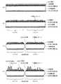
図7を参照して、従来の混成集積回路装置100の構成を説明する。 With reference to FIG. 7, the configuration of a conventional hybrid integrated circuit device 100 will be described.
図7(A)を参照して、従来の混成集積回路装置100Aの構成を説明する。矩形の基板101の表面には、絶縁層102を介して導電パターン103が形成されている。そして、導電パターン103の所望の箇所に回路素子が固着されることで、所定の電気回路が形成される。ここでは、回路素子として半導体素子105Aおよびチップ素子105Bが、導電パターン103に接続されている。半導体素子105Aの裏面は、半田等の接合材106を介して導電パターン103に固着されている。チップ素子105Bの両端の電極は、接合材106を介して導電パターン103に固着されている。リード104は、基板101の周辺部に形成された導電パターン103に接続され、外部端子として機能している。 A configuration of a conventional hybrid integrated circuit device 100A will be described with reference to FIG. A conductive pattern 103 is formed on the surface of the rectangular substrate 101 through an insulating layer 102. And a predetermined electric circuit is formed by fixing a circuit element to the desired location of the conductive pattern 103. Here, the semiconductor element 105 </ b> A and the chip element 105 </ b> B are connected to the conductive pattern 103 as circuit elements. The back surface of the semiconductor element 105A is fixed to the conductive pattern 103 via a bonding material 106 such as solder. The electrodes at both ends of the chip element 105 </ b> B are fixed to the conductive pattern 103 through the bonding material 106. The
しかしながら、上述した混成集積回路装置100Aでは、温度変化による応力により、接合材106にクラックが入る問題があった。チップ素子105Bを例にこの問題を説明すると、アルミニウムを基板101の材料とした場合、基板101の熱膨張係数は、23×10−6/℃である。それに対して、チップ素子105の熱膨張係数は小さい。具体的には、チップ抵抗の熱膨張係数は7×10−6/℃であり、チップコンデンサの熱膨張係数は、10×10−6/℃である。従って、チップ素子105Bと基板101との熱膨張係数が大きく相違するために、温度変化の際には、両者を結合する接合材106に大きな応力が作用する。従って、接合材106にクラックが発生して、接続不良の問題が起こる。However, the above-described hybrid integrated circuit device 100A has a problem that the bonding material 106 cracks due to stress due to temperature change. This problem will be described taking the chip element 105B as an example. When aluminum is used as the material of the substrate 101, the thermal expansion coefficient of the substrate 101 is 23 × 10−6 / ° C. In contrast, the thermal expansion coefficient of the chip element 105 is small. Specifically, the thermal expansion coefficient of the chip resistor is 7 × 10⁻⁶ / ° C., and the thermal expansion coefficient of the chip capacitor is 10 × 10−6 / ° C. Accordingly, since the thermal expansion coefficients of the chip element 105B and the substrate 101 are greatly different, a large stress acts on the bonding material 106 that couples the two when the temperature changes. Therefore, a crack occurs in the bonding material 106, causing a problem of poor connection.
図7(B)を参照して、接合材106のクラックを抑止する構造を説明する(下記特許文献1を参照)。ここでは、チップ素子105Bおよび接合材106が被覆樹脂108により被覆されている。ここで、被覆樹脂108の熱膨張係数は、アルミから成る基板101の熱膨張係数(23×10−6/℃)とほぼ等しくなっている。このことにより、熱膨張係数の小さいチップ素子105Bが、アルミニウム基板101と実質熱膨張係数が等しい被覆樹脂108により囲まれることで、温度変化の際に接合材106に加わる応力を低減させることができる。With reference to FIG. 7 (B), the structure which suppresses the crack of the joining material 106 is demonstrated (refer the following patent document 1). Here, the chip element 105 </ b> B and the bonding material 106 are covered with the covering resin 108. Here, the thermal expansion coefficient of the coating resin 108 is substantially equal to the thermal expansion coefficient (23 × 10−6 / ° C.) of the substrate 101 made of aluminum. As a result, the chip element 105B having a small thermal expansion coefficient is surrounded by the coating resin 108 having substantially the same thermal expansion coefficient as that of the aluminum substrate 101, so that the stress applied to the bonding material 106 when the temperature changes can be reduced. .
図7(C)に示す混成集積回路装置100Cでは、基板101に近似した熱膨張係数を有する封止樹脂109により、基板101の表面および側面を全面的に被覆している。ここで、封止樹脂109はトランスファーモールドにより形成される。
しかしながら、基板101に近似した熱膨張係数の封止樹脂109を用いて、基板101の表面を全面的に封止した場合、封止樹脂109の硬化収縮により、基板101が反る問題が発生する。これは、封止樹脂109の熱膨張係数を大きくすると、熱硬化時の硬化収縮の量も大きくなることが原因である。特に、基板101の平面的な大きさが6cm×4cm程度以上に大きい場合、この反りの問題が顕著に発生する。更に、図7(C)に示すように、基板101の裏面が封止樹脂109から露出する場合は、基板101の上方に大きな収縮応力が作用するので、基板101に対して強い曲げ応力が作用する。また、装置全体が大きく反ることにより、放熱フィン等の放熱体に装置を当接させることができない問題もあった。 However, when the sealing resin 109 having a thermal expansion coefficient approximate to that of the substrate 101 is used to completely seal the surface of the substrate 101, there is a problem that the substrate 101 warps due to curing shrinkage of the sealing resin 109. . This is because when the thermal expansion coefficient of the sealing resin 109 is increased, the amount of cure shrinkage during thermosetting is also increased. In particular, when the planar size of the substrate 101 is larger than about 6 cm × 4 cm, the problem of warpage is remarkably generated. Further, as shown in FIG. 7C, when the back surface of the substrate 101 is exposed from the sealing resin 109, a large contraction stress acts on the substrate 101, so that a strong bending stress acts on the substrate 101. To do. In addition, there is a problem that the apparatus cannot be brought into contact with a heat radiating body such as a heat radiating fin due to a large warpage of the entire apparatus.
本発明の回路装置では、回路基板の表面に設けられた導電パターンと、前記導電パターンに電気的に接続された回路素子と、少なくとも前記回路基板の表面を被覆して前記回路素子を封止する封止樹脂とを具備する回路装置に於いて、前記封止樹脂の熱膨張係数を、フィラーが入った状態で、前記回路基板の熱膨張係数よりも小さくすることを特徴とする。 In the circuit device of the present invention, the conductive pattern provided on the surface of the circuit board, the circuit element electrically connected to the conductive pattern, and at least the surface of the circuit board are covered to seal the circuit element. In a circuit device comprising a sealing resin, the thermal expansion coefficient of the sealing resin is made smaller than the thermal expansion coefficient of the circuit board in a state where a filler is contained.
更に本発明の回路装置では、前記回路基板の裏面は、前記封止樹脂から露出することを特徴とする。 Furthermore, in the circuit device of the present invention, the back surface of the circuit board is exposed from the sealing resin.
更に本発明の回路装置では、前記封止樹脂は、トランスファーモールドにより形成されることを特徴とする。 Furthermore, in the circuit device of the present invention, the sealing resin is formed by transfer molding.
更に本発明の回路装置では、前記回路基板は、アルミニウムから成る基板であり、前記封止樹脂の熱膨張係数は、フィラーが入った状態で15×10−6/℃から23×10−6/℃までの範囲であることを特徴とする。Furthermore, in the circuit device according to the present invention, the circuit board is a board made of aluminum, and the thermal expansion coefficient of the sealing resin is 15 × 10−6 / ° C. to 23 × 10−6 / in a state where a filler is contained. It is characterized by being in the range up to ° C.
更に本発明の回路装置では、前記回路素子は、鉛フリー半田を介して前記導電パターンに固着されることを特徴とする。 Furthermore, in the circuit device of the present invention, the circuit element is fixed to the conductive pattern via lead-free solder.
本発明の回路装置の製造方法は、導電パターンおよび回路素子から成る電気回路を回路基板の表面に形成する工程と、前記回路素子が被覆されるように少なくとも前記回路基板の表面をフィラー入り封止樹脂で被覆する工程とを具備し、前記回路基板よりも熱膨張係数の小さい前記封止樹脂を用いることを特徴とする。 The method for manufacturing a circuit device according to the present invention includes a step of forming an electric circuit comprising a conductive pattern and a circuit element on the surface of the circuit board, and at least the surface of the circuit board is sealed with a filler so as to cover the circuit element. And the step of coating with resin, wherein the sealing resin having a smaller coefficient of thermal expansion than that of the circuit board is used.
更に本発明の回路装置の製造方法は、導電パターンおよび回路素子から成る電気回路を回路基板の表面に形成する工程と、前記回路素子が被覆されるように少なくとも前記回路基板の表面をフィラー入り封止樹脂で被覆する工程と、前記封止樹脂を加熱することにより、前記回路基板が裏面の方向に湾曲した状態で、前記封止樹脂を硬化させる工程と、前記回路基板の湾曲を低減させた状態で、前記封止樹脂または前記回路基板の裏面を、放熱体の表面に当接させる工程とを具備することを特徴とする。 The circuit device manufacturing method of the present invention further includes a step of forming an electric circuit comprising a conductive pattern and a circuit element on the surface of the circuit board, and at least the surface of the circuit board is sealed with a filler so as to cover the circuit element. The step of coating with a stop resin, the step of curing the sealing resin in a state where the circuit board is curved in the direction of the back surface by heating the sealing resin, and the bending of the circuit board are reduced. And a step of bringing the sealing resin or the back surface of the circuit board into contact with the surface of the radiator in a state.
更に本発明の回路装置の製造方法では、前記封止樹脂は、トランスファーモールドにより形成される熱硬化性樹脂であることを特徴とする。 Furthermore, in the method for manufacturing a circuit device according to the present invention, the sealing resin is a thermosetting resin formed by transfer molding.
更に本発明の回路装置の製造方法では、前記封止樹脂の熱膨張係数を、前記回路基板よりも小さくすることを特徴とする。 Furthermore, in the method for manufacturing a circuit device of the present invention, the thermal expansion coefficient of the sealing resin is made smaller than that of the circuit board.
更に本発明の回路装置の製造方法では、前記回路基板はアルミニウムから成り、前記封止樹脂の熱膨張係数を、15×10−6/℃から23×10−6/℃の範囲にすることを特徴とする。Furthermore, in the circuit device manufacturing method of the present invention, the circuit board is made of aluminum, and the thermal expansion coefficient of the sealing resin is in the range of 15 × 10−6 / ° C. to 23 × 10−6 / ° C. Features.
更に、本発明の回路装置の製造方法は、銅を主材料とする導電パターンが形成されたアルミニウムまたは銅の基板を用意し、前記基板に回路素子を実装し、前記基板の少なくとも表面を実質カバーするように、樹脂をトランスファーモールドして製造する回路装置の製造方法であり、前記モールド時の前記樹脂の硬化収縮が抑制され、硬化した後の基板裏面が若干下に凸に成るように、フィラーが混入された樹脂の熱膨張係数が15×10−6/℃から23×10−6/℃の範囲で選択することを特徴とする。Furthermore, in the method for manufacturing a circuit device of the present invention, an aluminum or copper substrate on which a conductive pattern mainly composed of copper is formed is prepared, a circuit element is mounted on the substrate, and at least a surface of the substrate is substantially covered. And a method of manufacturing a circuit device by manufacturing a resin by transfer molding, wherein the resin shrinkage during the molding is suppressed, and the back surface of the substrate after curing is slightly convex downward The thermal expansion coefficient of the resin mixed with is selected from the range of 15 × 10−6 / ° C. to 23 × 10−6 / ° C.
一般に、応力を考える場合、液状または流動状の封止樹脂が硬化して固体になる場合の収縮と、硬化後の樹脂の熱による膨張収縮は、別に考える必要がある。 In general, when considering the stress, it is necessary to consider separately the contraction when the liquid or fluid sealing resin is cured to become a solid and the expansion and contraction due to the heat of the resin after curing.
図7(B)の様に、硬化した後は、基板101と被覆樹脂108は、実質熱膨張係数が等しいことが好ましい。つまり樹脂自体は、常に圧縮力が半田に加わり、また基板の伸び縮みと封止樹脂の伸び縮みが一致するため、半田に応力が加わりにくい。また液状または流動状の封止樹脂が図7Bの様に、部分的に塗布されて硬化して固体になる場合、この収縮力に対して、十分に基板が強いため、反りの問題は考える必要が無かった。 As shown in FIG. 7B, it is preferable that the substrate 101 and the coating resin 108 have substantially the same thermal expansion coefficient after being cured. That is, in the resin itself, a compressive force is always applied to the solder, and since the expansion / contraction of the substrate and the expansion / contraction of the sealing resin coincide with each other, it is difficult to apply stress to the solder. In addition, when the liquid or fluid sealing resin is partially applied and cured as shown in FIG. 7B to become a solid, the substrate is sufficiently strong against this contraction force, so the problem of warpage needs to be considered. There was no.
しかし図7Cの様に、被覆される樹脂の量(体積)が多くなればなるほど、液状または流動状の封止樹脂の硬化収縮は、大きくなる。そしてこの収縮力が大きいために、基板の反りが発生する。 However, as shown in FIG. 7C, the curing shrinkage of the liquid or fluid sealing resin increases as the amount (volume) of the resin to be coated increases. And since this contraction force is large, the curvature of a board | substrate generate | occur | produces.
この反りを抑止するために、本願では、樹脂の熱膨張係数は、実質アルミニウム基板と同じ材料を選択し、収縮を抑止するために、フィラーを約80%程度混入させている。このフィラーは、もともと固体であり、硬化収縮が無いため、封止樹脂全体の硬化時の収縮が小さくなる。そして硬化後のフィラー入り樹脂で考えると、熱膨張係数が約15×10−6/℃から23×10−6/℃の範囲であることが好ましい。In order to suppress this warpage, in the present application, a material having substantially the same thermal expansion coefficient as that of the aluminum substrate is selected, and about 80% of filler is mixed to suppress shrinkage. Since this filler is originally solid and has no curing shrinkage, the shrinkage at the time of curing of the entire sealing resin is reduced. And considering the resin containing filler after curing, the thermal expansion coefficient is preferably in the range of about 15 × 10−6 / ° C. to 23 × 10−6 / ° C.
つまり、硬化時の収縮を抑止するには、フィラーを入れればよく、また硬化後のフィラー入り封止樹脂の熱膨張係数ができる限り、アルミ基板に近いことが好ましいが、硬化収縮分を考慮すると、アルミより若干熱膨張係数が小さいほうが基板の膨張収縮とのバランスがとれる。 In other words, in order to suppress shrinkage at the time of curing, it is sufficient to add a filler, and as long as the thermal expansion coefficient of the sealing resin with filler after curing is as close as possible, it is preferable to be close to an aluminum substrate, but considering the amount of curing shrinkage When the coefficient of thermal expansion is slightly smaller than that of aluminum, a balance with expansion and contraction of the substrate can be obtained.
回路基板よりも若干熱膨張係数が小さいフィラー入りの封止樹脂を用いるので、封止樹脂を形成する際に生じる硬化収縮を低減させることができる。従って、封止樹脂の硬化収縮による剥離等を防止することができる。更に、装置全体の反りも抑制されている。 Since a sealing resin containing a filler having a slightly smaller thermal expansion coefficient than that of the circuit board is used, curing shrinkage that occurs when the sealing resin is formed can be reduced. Therefore, peeling due to curing shrinkage of the sealing resin can be prevented. Further, the warpage of the entire apparatus is also suppressed.
更に、本発明の回路装置の製造方法によれば、封止樹脂の硬化収縮により回路基板を裏面方向に若干湾曲させ、封止樹脂または回路基板を放熱体に当接させることにより、封止樹脂または回路基板の裏面を、放熱体に密着させることができ、放熱性を向上させることができる。 Furthermore, according to the method for manufacturing a circuit device of the present invention, the sealing resin is obtained by slightly curving the circuit board in the back surface direction by curing shrinkage of the sealing resin, and bringing the sealing resin or the circuit board into contact with the radiator. Or the back surface of a circuit board can be stuck to a heat radiator, and heat dissipation can be improved.
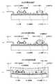
<混成集積回路装置10の構成>
図1を参照して、本発明の混成集積回路装置10の構成を説明する。先ず、矩形の回路基板11の表面には、絶縁層18が形成されている。そして、所定の形状の導電パターン13が、絶縁層18の表面に形成されている。更に、導電パターン13の所定の箇所には、半導体素子15Aおよびチップ素子15Bが電気的に接続されている。回路基板11の表面に形成された導電パターン13、半導体素子15Aおよびチップ素子15Bは、封止樹脂14により被覆されている。<Configuration of Hybrid Integrated Circuit Device 10>
The configuration of the hybrid integrated circuit device 10 of the present invention will be described with reference to FIG. First, an insulating
回路基板11は、アルミニウムや銅等の金属から成る基板である。回路基板11の材料としてアルミニウムを採用した場合、回路基板11の熱膨張係数は、23×10−6/℃程度である。回路基板11の具体的な大きさは、例えば縦×横×厚さ=61mm×42.5mm×1.5mm程度である。The circuit board 11 is a board made of a metal such as aluminum or copper. When aluminum is adopted as the material of the circuit board 11, the thermal expansion coefficient of the circuit board 11 is about 23 × 10−6 / ° C. The specific size of the circuit board 11 is, for example, about vertical × horizontal × thickness = 61 mm × 42.5 mm × 1.5 mm.
回路基板11の側面は、第1の傾斜部S1および第2の傾斜部S2からなり外部に突出している。第1の傾斜部S1は、回路基板11の上面から連続して斜め下方に延在している。第2の傾斜部S2は、回路基板11の下面から連続して斜め上方に延在している。この構成により、回路基板11の側面と封止樹脂との密着を強固にすることができる。尚、回路基板11の側面は、平坦面でも良い。 The side surface of the circuit board 11 includes a first inclined portion S1 and a second inclined portion S2, and protrudes to the outside. The first inclined portion S <b> 1 extends obliquely downward continuously from the upper surface of the circuit board 11. The second inclined portion S <b> 2 extends obliquely upward continuously from the lower surface of the circuit board 11. With this configuration, the adhesion between the side surface of the circuit board 11 and the sealing resin can be strengthened. The side surface of the circuit board 11 may be a flat surface.
回路基板11の表面および裏面には、第1の酸化膜12Aおよび第2の酸化膜12Bが形成されている。 A first oxide film 12A and a second oxide film 12B are formed on the front surface and the back surface of the circuit board 11.
第1の酸化膜12Aは、回路基板11の表面全域を覆うように形成されている。具体的には、第1の酸化膜12Aの組成式はAl2O3であり、厚みは1μmから5μmの範囲である。回路基板11の表面に第1の酸化膜12Aを形成することにより、絶縁層18の密着性を向上させることができる。本形態では、第1の酸化膜12Aが非常に薄く形成される。従って、半導体素子15A等から発生した熱を、効率よく外部に放出することができる。また、第1の酸化膜12Aの厚みは、絶縁層18と回路基板11との密着性が確保できれば、1μm以下でも良い。The
第2の酸化膜12Bは、回路基板11の裏面全域を覆うように形成されている。第2の酸化膜12Bは、第1の酸化膜12Aと同様にAl2O3から成り、厚みは7μmから13μm程度の範囲である。第2の酸化膜12Bは、各製造工程にて、回路基板11の裏面を機械的に保護する役割を有する。更に、第2の酸化膜12Bは、ウェットエッチングにより導電パターン13をパターニングする工程にて、回路基板11の裏面をエッチャントから保護する役割を有する。従って、第2の酸化膜12Bは、第1の酸化膜12Aよりも厚く形成される。また、第2の酸化膜12Bを厚くすることにより、封止樹脂14の硬化収縮による回路素子15の反りを低減させることもできる。The
絶縁層18は、回路基板11の表面全域を覆うように形成されている。絶縁層18は、AL2O3等のフィラーが高充填されたエポキシ樹脂から成る。フィラーが充填されることにより、絶縁層18の熱抵抗が低減されている。従って、内蔵される回路素子から発生した熱は、回路基板11を介して良好に外部に放出される。The insulating
導電パターン13は銅等の金属から成り、所定の電気回路が実現されるように絶縁層18の表面に形成される。また、リード16が導出する辺に、導電パターン13からなるパッドが形成される。 The
半導体素子15Aおよびチップ素子15Bの回路素子は、半田等の接合材を介して、導電パターン13の所定の箇所に固着されている。半導体素子15Aとしては、トランジスタ、LSIチップ、ダイオード等が採用される。ここでは、半導体素子15Aと導電パターン13とは、金属細線17を介して接続される。チップ素子15Bとしては、チップ抵抗やチップコンデンサ等が採用される。チップ素子15Bの両端の電極は、半田等の接合材を介して導電パターン13に固着されている。更に、チップ素子15Bとしては、インダクタンス、サーミスタ、アンテナ、発振器など、両端に電極部を有する素子が採用される。更にまた、樹脂封止型のパッケージ等も、回路素子として導電パターン13に固着することができる。 The circuit elements of the semiconductor element 15A and the chip element 15B are fixed to predetermined portions of the
回路素子を接合させる接合材としては、半田または導電性ペースト等が採用される。ここで、半田としては、鉛共晶半田または鉛フリー半田を用いることができる。導電性ペーストとしては、Agペースト、Cuペースト等が採用される。 As a bonding material for bonding circuit elements, solder, conductive paste, or the like is employed. Here, as the solder, lead eutectic solder or lead-free solder can be used. As the conductive paste, Ag paste, Cu paste or the like is employed.
鉛フリー半田を用いて回路素子を固着する場合は、熱応力によるクラックの発生に留意する必要がある。その理由は、鉛フリー半田はヤング率が大きく、クラックが生じやすい材料であるからである。一例として、鉛共晶半田のヤング率が25.8GPaであるのに対して、Sn−3.0Ag−0.5Cuの組成を有する鉛フリー半田のヤング率は41.6GPaである。鉛フリー半田としては、具体的には、Sn−Ag系、Sn−Ag−Cu系、Sn−Cu系、Sn−Zn系、または、これらにBiやInを添加した組成のものを採用することができる。 When fixing circuit elements using lead-free solder, it is necessary to pay attention to the occurrence of cracks due to thermal stress. This is because lead-free solder has a high Young's modulus and is prone to cracking. As an example, the Young's modulus of lead eutectic solder is 25.8 GPa, while the Young's modulus of lead-free solder having a composition of Sn-3.0Ag-0.5Cu is 41.6 GPa. Specifically, as the lead-free solder, Sn-Ag, Sn-Ag-Cu, Sn-Cu, Sn-Zn, or a composition in which Bi or In is added to these is adopted. Can do.
リード16は、回路基板11の周辺部に設けられたパッドに固着され、外部との入力・出力を行う働きを有する。ここでは、1つの辺に多数個のリード16が設けられている。リード16は回路基板11の4辺から導出させることも可能であり、対向する2つの辺から導出させることも可能である。 The
封止樹脂14は、熱硬化性樹脂を用いるトランスファーモールドにより形成される。図1(B)では、封止樹脂14により、導電パターン13、半導体素子15A、チップ素子15B、金属細線17が封止されている。そして、回路基板11の表面および側面が封止樹脂14により被覆されている。回路基板11の裏面は、封止樹脂14から外部に露出している。更に、図1(C)に示すように、裏面も含めた回路基板11の全体が封止樹脂14により被覆されても良い。また、熱硬化性樹脂から成る封止樹脂14は、硬化する際に収縮するので、回路素子や半田等に圧縮応力を与え続ける。 The sealing
本形態では、回路基板11の熱膨張係数と実質同じ封止樹脂を選択し、この中に酸化アルミニウムフィラーを入れることにより、樹脂自体の体積を減らし、これにより樹脂の硬化時の収縮を抑制している。例えばフィラーは、約80%混入している。 In this embodiment, a sealing resin that has substantially the same thermal expansion coefficient as that of the circuit board 11 is selected, and an aluminum oxide filler is placed therein, thereby reducing the volume of the resin itself, thereby suppressing shrinkage when the resin is cured. ing. For example, about 80% of filler is mixed.
また、基板が両サイドでネジ等で加圧されて実装されるので、硬化後、常温で、図2Bの如く、若干下に凸の形状である必要がある。 Further, since the substrate is mounted by being pressed with screws or the like on both sides, it needs to have a slightly downward convex shape at room temperature after curing as shown in FIG. 2B.
つまりフィラー入りの封止樹脂14の熱膨張係数を、回路基板11の熱膨張係数よりも小さくしている。このことにより、封止樹脂14の熱収縮による回路基板11の反りを防止することができ、更には硬化後の基板を若干下に凸とでき、しかも実装時の熱による伸び縮みをアルミ基板にできる限り近づけているため、ロウ材等のクラックも抑止できる特徴がある。 That is, the thermal expansion coefficient of the sealing
背景技術の欄にて説明したように、アルミ基板を回路基板11として採用した場合は、回路基板11とチップ素子15Bとの熱膨張係数が大きく相違する。従って、両者を接続する半田には、大きな熱応力が作用する。このことから、封止樹脂14の熱膨張係数を、回路基板11と同等に23×10−6/℃程度にすることで、熱応力を低減していた。As described in the Background Art section, when an aluminum substrate is employed as the circuit board 11, the thermal expansion coefficients of the circuit board 11 and the chip element 15B are greatly different. Therefore, a large thermal stress acts on the solder connecting the two. From this, the thermal stress was reduced by setting the thermal expansion coefficient of the sealing
しかしながら、熱硬化性樹脂は、熱硬化する際、収縮が働く。従って、23×10−6/℃程度以上の熱膨張係数を有する封止樹脂14を用いた場合、熱硬化による収縮の量が大きくなり、回路基板11が過度に反ってしまう問題が発生する場合がある。However, the thermosetting resin contracts when it is thermoset. Therefore, when the sealing
このことから、本形態では、フィラーを入れて硬化時の収縮を抑止し、フィラーも含めた封止樹脂14の熱膨張係数を15×10−6/℃〜23×10−6/℃の間に設定している。このことにより、回路素子の接続信頼性を確保しつつ、熱硬化時の回路基板11の反りを防止できる。実験によると、フィラー入り樹脂の熱膨張係数を上記範囲で用いると、封止樹脂14の熱膨張係数が23×10−6/℃である場合と比較して、回路素子15の接続信頼性を同程度にすることができる。更に、本装置の反りを低減することができる。Therefore, in this embodiment, a filler is added to suppress shrinkage at the time of curing, and the thermal expansion coefficient of the sealing
図2を参照して、封止樹脂14の熱膨張係数と、混成集積回路装置10の反りとの関係を説明する。図2(A)は、両者の関係を示すグラフである。図2(B)および図2(C)は、反った状態の混成集積回路装置10の断面図である。 The relationship between the thermal expansion coefficient of the sealing
図2(A)に示すグラフの横軸は、フィラー入りの封止樹脂14の熱膨張係数を示している。縦軸は、混成集積回路装置10の反りの量を示している。ここでは、フィラーの混入量を調整し、熱膨張係数の異なる封止樹脂14を用いて複数個の混成集積回路装置10の樹脂封止および加熱硬化を行い、各混成集積回路装置10に発生する反りの量を測定した。具体的な反りの量の計測方法は、先ず、加熱硬化を終えた混成集積回路装置10を、平坦面に載置する。そして、混成集積回路装置10の上面の高さを計測して、その高低差を混成集積回路装置10の反りの量とした。白抜きの円で示す各点は、実験結果を示している。そして、点線の曲線は、これらの実験結果から算出した近似曲線Lである。 The horizontal axis of the graph shown in FIG. 2A indicates the thermal expansion coefficient of the sealing
グラフに示す実験結果から、熱膨張係数が大きい封止樹脂(フィラーの少ないもの)を用いると、混成集積回路装置10の反りの量が大きくなることが理解できる。例えば、熱膨張係数が15×10−6/℃程度の封止樹脂(フィラーが多いもの)14を用いると、反りが発生していない平坦な混成集積回路装置10を得ることができる。また、封止樹脂14の熱膨張係数の増加に伴って、装置に発生する反りの量も増加する。From the experimental results shown in the graph, it can be understood that the amount of warpage of the hybrid integrated circuit device 10 increases when a sealing resin having a large thermal expansion coefficient (a material having a small amount of filler) is used. For example, when a sealing resin (having a large amount of filler) 14 having a thermal expansion coefficient of about 15 × 10−6 / ° C. is used, a flat hybrid integrated circuit device 10 with no warpage can be obtained. Further, as the thermal expansion coefficient of the sealing
封止樹脂14の熱膨張係数が15×10−6/℃程度以上では、反りの量がプラスの値になっており、熱膨張係数の増加に伴い、混成集積回路装置10の反りは大きくなる。反りの量がプラスの値のときは、図2(B)に示すような断面形状となる。即ち、混成集積回路装置10に内蔵された回路基板11が裏面の方向に湾曲されている。そして、装置全体は、下方に凸状になるように湾曲している。この断面形状であれば、装置の両端を下方に押圧することにより、装置全体を平坦にすることができる。When the thermal expansion coefficient of the sealing
フィラー入りの封止樹脂14の熱膨張係数が15×10−6/℃未満では、反りの量がマイナスの値になっている。反りの量がマイナスの場合は、混成集積回路装置10の断面形状は図2(C)に示すような状態になる。即ち、装置全体が上方に対して凸状に湾曲している。この状態では、装置の両端を下方に押圧しても、装置全体が平坦にならない。混成集積回路装置10の裏面を放熱フィン等に当接させても、両者の間に間隙が形成される。従って、混成集積回路装置10の放熱性が低下してしまう。When the thermal expansion coefficient of the sealing
本形態では、フィラー入りの封止樹脂14の熱膨張係数を、15×10−6/℃から23×10−6/℃の範囲に設定している。In this embodiment, the thermal expansion coefficient of the filler-containing
封止樹脂14の熱膨張係数を23×10−6/℃以下にすることにより、混成集積回路装置10の反りの量を一定以下にすることができる。具体的には、この反りの量を50μm以下にすることができる。更に、硬化収縮による応力をフィラーが入ることで小さくすることができる。従って、装置内部の電気回路が硬化収縮により破壊されるのを抑止することができる。しかも硬化後の温度の上下による装置の伸び縮みは、ある程度同等で働く範囲にすることにより、信頼性の向上を実現できる。特に、半田等のロウ材から成る接続部には、常に圧縮応力が働くので、クラックが入るのを抑止することができる。By setting the thermal expansion coefficient of the sealing
更に、フィラー入りの封止樹脂14の熱膨張係数を15×10−6/℃以上にすることで、混成集積回路装置10が上方向に凸状に反るのを抑止することができる。即ち、混成集積回路装置10の断面形状が図2(C)にように成るのを抑止することができる。図2(C)に示すような反りが発生すると、装置の裏面が放熱体に密着せず、放熱性が低下してしまう。Furthermore, by making the thermal expansion coefficient of the sealing
<混成集積回路装置10の製造方法>
図3から図6を参照して、混成集積回路装置の製造方法を説明する。<Method for Manufacturing Hybrid Integrated Circuit Device 10>
A method for manufacturing a hybrid integrated circuit device will be described with reference to FIGS.
図3(A)を参照して、先ず、絶縁層18を介して導電箔20を金属基板19の表面に貼着する。金属基板19の表面には第1の酸化膜12Aが全面的に形成されている。従って、第1の酸化膜12Aと絶縁層18とが電気的に結合することにより、絶縁層18と金属基板19とは接着している。更に、ウエットエッチングを行うことにより、導電箔20をパターニングして、導電パターン13が形成される。導電箔20のエッチングは、金属基板19全体をエッチャントに浸漬して行われる。 Referring to FIG. 3A, first,
図3(B)に導電パターン13が形成された後の金属基板19の断面を示す。ここでは、金属基板19の表面には、導電パターン13から成るユニット21が複数個形成される。ここで、ユニットとは、1つの混成集積回路装置を構成する部位である。ユニット21は、マトリックス状に複数個が形成されても良い。 FIG. 3B shows a cross section of the
図3(C)を参照して、次に、金属基板19の表面および裏面に、第1の溝22Aおよび第2の溝22Bを形成する。第1の溝22Aおよび第2の溝22Bは、高速で回転するカットソーを用いて形成される。 Referring to FIG. 3C, next, first groove 22A and second groove 22B are formed on the front surface and the back surface of
図3(D)を参照して、次に、回路素子を導電パターン13に電気的に接続する。ここでは、半導体素子15Aやチップ素子15B等の回路素子が、半田等を介して導電パターン13に固着されている。更に、半導体素子15Aの表面の電極は、金属細線を介して導電パターン13と電気的に接続されている。更に、半導体素子15Aは、導電パターン13に固着されたヒートシンク25の上面に載置されても良い。 Next, referring to FIG. 3D, the circuit element is electrically connected to the
図4を参照して、次に、金属基板19を分離する工程を説明する。金属基板19を分離する方法としては、「折り曲げ」による分割方法と、「切断」による分割方法の2つの方法が採用できる。 Next, a process of separating the
図4(A)を参照して、「折り曲げ」により金属基板19を分離する方法を説明する。ここでは、第1の溝22Aおよび第2の溝22Bが形成された箇所を支点にして、金属基板19を曲折させている。この図では、紙面上で右側に位置するユニット21が固定され、左側に位置するユニット21が曲折されている。この曲折を上下方向に複数回行うことで、ユニット21どうしは分離される。本形態では、ユニット21どうしの境界には、第1および第2の溝22A、22Bが形成されている。従って、各ユニット21は、溝が形成されていない厚み部分のみで連結されている。このことから、上述した「折り曲げ」による分離は容易に行うことができる。 With reference to FIG. 4A, a method of separating the
図4(B)を参照して、切断による金属基板19の分離方法を説明する。ここでは、カッター23を、第1の溝22Aに押しつけながら回転させることで、金属基板19を分割している。カッター23は円板状の形状を有しており、その周端部は鋭角に形成してある。カッター23の中心部は、カッター23が自在に回転できるように支持部24に固定してある。即ち、カッター23は駆動力を有さない。カッター23を第1の溝22Aの底部に押し当てながら移動させることで、カッター23は回転し、金属基板19が分離される。この方法によると、切断を行うことによる導電性の粉塵が発生しない。従って、この粉塵によるショートを防止することができる。 With reference to FIG. 4B, a method of separating the
尚、上述以外の方法でも金属基板19を分離することができる。具体的には、プレス機を用いたパンチング、シャーリング等により金属基板19を分離することができる。 Note that the
図5を参照して、次に、少なくとも回路基板11の表面が被覆されるように封止樹脂14を形成する。ここでは、金型31を用いたトランスファーモールドにより、フィラー入りの熱硬化性樹脂から成る封止樹脂14を形成している。具体的には、金型31のキャビティ33に回路基板11を収納し、ゲート32からキャビティ33の内部に封止樹脂14を注入する。 Referring to FIG. 5, next, a sealing
封止樹脂14が封入されるとき、金型31は170℃程度に加熱されている。従って、熱硬化性樹脂から成る封止樹脂14は、キャビティ33に注入されると同時に、熱硬化が進行する。この熱硬化は、数十秒から百秒程度で行われる。熱硬化が行われることで封止樹脂14は硬化収縮するが、封止樹脂14の熱膨張係数は23×10−6/℃以下である。このことから、硬化収縮よる回路基板11の過度の反りは抑制されている。When the sealing
図6を参照して、次に、混成集積回路装置10を放熱フィンに当接させる。先ず、図6(A)に示すように、平坦面に形成された放熱フィン28の上面にグリス29を塗布する。放熱フィン28は、銅などの金属から成り、混成集積回路装置10から発生した熱を外部に放出させる機能を有する。また、グリス29は、混成集積回路装置10の裏面と放熱フィン28の上面との間に介在して、放熱性を向上させる働きを有する。グリス29は、混成集積回路装置10の中央部に対応する箇所に塗布される。 Next, referring to FIG. 6, the hybrid integrated circuit device 10 is brought into contact with the heat radiating fins. First, as shown in FIG. 6A, grease 29 is applied to the upper surface of the radiation fin 28 formed on the flat surface. The radiation fin 28 is made of a metal such as copper and has a function of releasing heat generated from the hybrid integrated circuit device 10 to the outside. The grease 29 is interposed between the rear surface of the hybrid integrated circuit device 10 and the upper surface of the heat radiation fin 28 and has a function of improving heat dissipation. The grease 29 is applied to a location corresponding to the central portion of the hybrid integrated circuit device 10.
次に、放熱フィン28の上部に混成集積回路装置10を載置した後に、その裏面を放熱フィン28の上面に当接させる。具体的には、混成集積回路装置10の両端に設けた固定部26を、ビス30により下方に押圧することで、混成集積回路装置10の裏面を放熱フィン28の上部に密着させる。混成集積回路装置10は、封止樹脂14の熱硬化により、下方に突出するように湾曲している。従って、ビス30の押圧力により、湾曲した混成集積回路装置10を平坦化させることにより、中央部に塗布されたグリス29を、周辺部に行き渡らせることができる。また、ビス30の押圧力により、混成集積回路装置10の湾曲は低減された状態で固定される。このことにより、混成集積回路装置10の裏面は放熱フィン28の上面に密着している。 Next, after the hybrid integrated circuit device 10 is placed on the upper portion of the heat radiation fin 28, the back surface thereof is brought into contact with the upper surface of the heat radiation fin 28. Specifically, the fixing portions 26 provided at both ends of the hybrid integrated circuit device 10 are pressed downward with screws 30, thereby bringing the back surface of the hybrid integrated circuit device 10 into close contact with the upper portion of the heat radiation fin 28. The hybrid integrated circuit device 10 is curved so as to protrude downward due to the thermosetting of the sealing
図6(B)を参照して、ビス30を用いて混成集積回路装置10の周辺部を押圧することにより、混成集積回路装置10の裏面は放熱フィン28の上面に密着されている。従って、混成集積回路装置10に内蔵された回路素子か発生した熱は、放熱フィン28を介して外部に放出される。この図では、封止樹脂14から露出する回路基板11の裏面が、放熱フィン28の上面に当接している。しかしながら、図1(C)に示すように、回路基板11の裏面が被覆されるように封止樹脂14が形成される場合もある。この場合は、封止樹脂14から成る混成集積回路装置10の裏面が、放熱フィン28の上面に当接する。 With reference to FIG. 6B, the back surface of the hybrid integrated circuit device 10 is brought into close contact with the upper surface of the radiation fin 28 by pressing the peripheral portion of the hybrid integrated circuit device 10 using the screws 30. Accordingly, the heat generated by the circuit elements incorporated in the hybrid integrated circuit device 10 is released to the outside through the heat radiation fins 28. In this figure, the back surface of the circuit board 11 exposed from the sealing
10 混成集積回路装置
11 回路基板
12A 第1の酸化膜
12B 第2の酸化膜
13 導電パターン
14 封止樹脂
15 回路素子
15A 半導体素子
15B チップ素子
16 リード
17 金属細線
18 絶縁層
19 金属基板
20 導電箔
21 ユニット
22A 第1の溝
22B 第2の溝
23 カッター
24 支持部
27 ビス
25 ヒートシンク
28 放熱フィン
29 グリス
30 ビス
31 金型
32 ゲート
DESCRIPTION OF SYMBOLS 10 Hybrid integrated circuit device 11 Circuit board 12A 1st oxide film 12B
Claims (11)
Translated fromJapanese前記導電パターンに電気的に接続された回路素子と、
少なくとも前記回路基板の表面を被覆して前記回路素子を封止する封止樹脂とを具備する回路装置に於いて、
前記封止樹脂の熱膨張係数を、フィラーが入った状態で、前記回路基板の熱膨張係数よりも小さくすることを特徴とする回路装置。A conductive pattern provided on the surface of the circuit board;
A circuit element electrically connected to the conductive pattern;
In a circuit device comprising a sealing resin that covers at least the surface of the circuit board and seals the circuit element,
A circuit device, wherein a thermal expansion coefficient of the sealing resin is made smaller than a thermal expansion coefficient of the circuit board in a state where a filler is contained.
前記封止樹脂の熱膨張係数は、フィラーが入った状態で15×10−6/℃から23×10−6/℃までの範囲であることを特徴とする請求項1記載の回路装置。The circuit board is a board made of aluminum,
2. The circuit device according to claim 1, wherein a thermal expansion coefficient of the sealing resin is in a range from 15 × 10−6 / ° C. to 23 × 10−6 / ° C. in a state where a filler is contained.
前記回路素子が被覆されるように少なくとも前記回路基板の表面をフィラー入り封止樹脂で被覆する工程とを具備し、
前記回路基板よりも熱膨張係数の小さい前記封止樹脂を用いることを特徴とする回路装置の製造方法。Forming an electrical circuit comprising a conductive pattern and circuit elements on the surface of the circuit board;
Covering at least the surface of the circuit board with a sealing resin containing a filler so that the circuit element is covered,
A method for manufacturing a circuit device, comprising using the sealing resin having a smaller thermal expansion coefficient than the circuit board.
前記回路素子が被覆されるように少なくとも前記回路基板の表面をフィラー入り封止樹脂で被覆する工程と、
前記封止樹脂を加熱することにより、前記回路基板が裏面の方向に湾曲した状態で、前記封止樹脂を硬化させる工程と、
前記回路基板の湾曲を低減させた状態で、前記封止樹脂または前記回路基板の裏面を、放熱体の表面に当接させる工程とを具備することを特徴とする回路装置の製造方法。Forming an electrical circuit comprising a conductive pattern and circuit elements on the surface of the circuit board;
Coating at least the surface of the circuit board with a sealing resin containing filler so that the circuit element is coated;
Curing the sealing resin in a state where the circuit board is curved in the direction of the back surface by heating the sealing resin;
And a step of bringing the sealing resin or the back surface of the circuit board into contact with the surface of the heat radiating body in a state in which the curvature of the circuit board is reduced.
前記封止樹脂の熱膨張係数を、15×10−6/℃から23×10−6/℃の範囲にすることを特徴とする請求項6または請求項7記載の回路装置の製造方法。The circuit board is made of aluminum;
8. The method of manufacturing a circuit device according to claim 6, wherein a thermal expansion coefficient of the sealing resin is in a range of 15 × 10−6 / ° C. to 23 × 10−6 / ° C.
前記基板に回路素子を実装し、
前記基板の少なくとも表面を実質カバーするように、樹脂をトランスファーモールドして製造する回路装置の製造方法であり、
前記モールド時の前記樹脂の硬化収縮が抑制され、硬化した後の基板裏面が若干下に凸に成るように、フィラーが混入された樹脂の熱膨張係数が15×10−6/℃から23×10−6/℃の範囲で選択することを特徴とした回路装置の製造方法。
Prepare an aluminum or copper substrate on which a conductive pattern mainly made of copper is formed,
A circuit element is mounted on the substrate,
A method of manufacturing a circuit device that is manufactured by transfer molding a resin so as to substantially cover at least the surface of the substrate,
Curing shrinkage of the resin during the molding is suppressed, and the thermal expansion coefficient of the resin mixed with the filler is 15 × 10−6 / ° C. to 23 × so that the back surface of the substrate after curing is slightly convex. A method for manufacturing a circuit device, wherein the selection is made in the range of 10−6 / ° C.
Priority Applications (5)
| Application Number | Priority Date | Filing Date | Title |
|---|---|---|---|
| JP2004288213AJP2006100752A (en) | 2004-09-30 | 2004-09-30 | Circuit arrangement and its manufacturing method |
| TW94102426ATWI271130B (en) | 2004-09-30 | 2005-01-27 | Circuit device and method of producing the same |
| KR20050013995AKR100726902B1 (en) | 2004-09-30 | 2005-02-21 | Circuit device and manufacturing method thereof |
| CNB2005100525405ACN100397627C (en) | 2004-09-30 | 2005-02-28 | Circuit device and manufacturing method thereof |
| US11/237,856US20060065421A1 (en) | 2004-09-30 | 2005-09-29 | Circuit device and manufacturing method thereof |
Applications Claiming Priority (1)
| Application Number | Priority Date | Filing Date | Title |
|---|---|---|---|
| JP2004288213AJP2006100752A (en) | 2004-09-30 | 2004-09-30 | Circuit arrangement and its manufacturing method |
Publications (1)
| Publication Number | Publication Date |
|---|---|
| JP2006100752Atrue JP2006100752A (en) | 2006-04-13 |
Family
ID=36097706
Family Applications (1)
| Application Number | Title | Priority Date | Filing Date |
|---|---|---|---|
| JP2004288213APendingJP2006100752A (en) | 2004-09-30 | 2004-09-30 | Circuit arrangement and its manufacturing method |
Country Status (5)
| Country | Link |
|---|---|
| US (1) | US20060065421A1 (en) |
| JP (1) | JP2006100752A (en) |
| KR (1) | KR100726902B1 (en) |
| CN (1) | CN100397627C (en) |
| TW (1) | TWI271130B (en) |
Cited By (6)
| Publication number | Priority date | Publication date | Assignee | Title |
|---|---|---|---|---|
| JP2007324274A (en)* | 2006-05-31 | 2007-12-13 | Sanyo Electric Co Ltd | Method of manufacturing circuit device |
| JP2007324394A (en)* | 2006-06-01 | 2007-12-13 | Denso Corp | Mold package and its manufacturing method |
| JP2011003680A (en)* | 2009-06-18 | 2011-01-06 | Hitachi Automotive Systems Ltd | Electronic circuit sealing device |
| US8219997B2 (en) | 2006-11-10 | 2012-07-10 | International Business Machines Corporation | Execution the job that is divided into job tasks based on the estimated completion time |
| US8383946B2 (en) | 2010-05-18 | 2013-02-26 | Joinset, Co., Ltd. | Heat sink |
| JP2016115810A (en)* | 2014-12-15 | 2016-06-23 | 株式会社デンソー | Electronic apparatus |
Families Citing this family (13)
| Publication number | Priority date | Publication date | Assignee | Title |
|---|---|---|---|---|
| WO2008120280A1 (en)* | 2007-03-29 | 2008-10-09 | Fujitsu Limited | Distortion reduction fixing structure |
| KR101011199B1 (en)* | 2007-11-01 | 2011-01-26 | 파나소닉 주식회사 | Mount structure |
| TWI322652B (en)* | 2007-11-06 | 2010-03-21 | Yu Hsueh Lin | Structure and manufacturing method of circuit substrate board |
| CN101944489B (en)* | 2009-07-07 | 2012-06-20 | 株式会社村田制作所 | Manufacturing method of composite substrate |
| JP2011100718A (en)* | 2009-10-05 | 2011-05-19 | Yazaki Corp | Connector |
| JP5774292B2 (en)* | 2010-11-04 | 2015-09-09 | セミコンダクター・コンポーネンツ・インダストリーズ・リミテッド・ライアビリティ・カンパニー | Circuit device and manufacturing method thereof |
| JP5796956B2 (en)* | 2010-12-24 | 2015-10-21 | セミコンダクター・コンポーネンツ・インダストリーズ・リミテッド・ライアビリティ・カンパニー | Circuit device and manufacturing method thereof |
| JP2013069748A (en)* | 2011-09-21 | 2013-04-18 | Toshiba Corp | Base plate and semiconductor device |
| JP2015018979A (en)* | 2013-07-12 | 2015-01-29 | イビデン株式会社 | Printed wiring board |
| DE102013219992A1 (en)* | 2013-10-02 | 2015-04-02 | Conti Temic Microelectronic Gmbh | Circuit device and method for its production |
| JP6483498B2 (en) | 2014-07-07 | 2019-03-13 | ローム株式会社 | Electronic device and its mounting structure |
| JP6693441B2 (en)* | 2017-02-27 | 2020-05-13 | オムロン株式会社 | Electronic device and manufacturing method thereof |
| DE102020204941A1 (en)* | 2020-04-20 | 2020-10-29 | Robert Bosch Gesellschaft mit beschränkter Haftung | Method and device for producing a substrate provided with a hardenable potting compound |
Citations (6)
| Publication number | Priority date | Publication date | Assignee | Title |
|---|---|---|---|---|
| JPH08298299A (en)* | 1995-04-27 | 1996-11-12 | Hitachi Ltd | Semiconductor device |
| JPH1079453A (en)* | 1996-09-05 | 1998-03-24 | Hitachi Ltd | Molded electronic component and manufacturing method thereof |
| JPH10135377A (en)* | 1996-11-01 | 1998-05-22 | Hitachi Ltd | Mold type semiconductor device |
| JPH1117071A (en)* | 1997-06-23 | 1999-01-22 | Hitachi Ltd | Semiconductor device |
| JP2003318312A (en)* | 2002-04-24 | 2003-11-07 | Sanyo Electric Co Ltd | Hybrid integrated circuit device |
| JP2004095735A (en)* | 2002-08-30 | 2004-03-25 | Kyocera Corp | Semiconductor device |
Family Cites Families (28)
| Publication number | Priority date | Publication date | Assignee | Title |
|---|---|---|---|---|
| US3658750A (en)* | 1969-02-13 | 1972-04-25 | Hitachi Ltd | Thermosetting resin composition and electrical appliances using the same |
| US4720424A (en)* | 1984-06-18 | 1988-01-19 | Hoebbst Celanese Corporation | Electronic component encapsulated with a composition comprising a polymer which is capable of forming an anisotropic melt phase and substantially incapable of further chain growth upon heating |
| US4754101A (en)* | 1986-10-23 | 1988-06-28 | Instrument Specialties Co., Inc. | Electromagnetic shield for printed circuit board |
| JP3163622B2 (en)* | 1990-07-05 | 2001-05-08 | 日産自動車株式会社 | Electric car |
| US5136366A (en)* | 1990-11-05 | 1992-08-04 | Motorola, Inc. | Overmolded semiconductor package with anchoring means |
| JP2951102B2 (en)* | 1991-05-23 | 1999-09-20 | 三洋電機株式会社 | Hybrid integrated circuit |
| US5369056A (en)* | 1993-03-29 | 1994-11-29 | Staktek Corporation | Warp-resistent ultra-thin integrated circuit package fabrication method |
| KR970011623B1 (en)* | 1994-01-13 | 1997-07-12 | Samsung Electronics Co Ltd | Lead frame of semiconductor package |
| US5773895A (en)* | 1996-04-03 | 1998-06-30 | Intel Corporation | Anchor provisions to prevent mold delamination in an overmolded plastic array package |
| JP3398004B2 (en)* | 1997-03-24 | 2003-04-21 | ローム株式会社 | Package type semiconductor device structure |
| US6011301A (en)* | 1998-06-09 | 2000-01-04 | Stmicroelectronics, Inc. | Stress reduction for flip chip package |
| US6143981A (en)* | 1998-06-24 | 2000-11-07 | Amkor Technology, Inc. | Plastic integrated circuit package and method and leadframe for making the package |
| US6448633B1 (en)* | 1998-11-20 | 2002-09-10 | Amkor Technology, Inc. | Semiconductor package and method of making using leadframe having lead locks to secure leads to encapsulant |
| FI982586L (en)* | 1998-11-30 | 2000-05-31 | Nokia Mobile Phones Ltd | Electronic device |
| US6178097B1 (en)* | 1999-01-22 | 2001-01-23 | Dial Tool Industries, Inc. | RF shield having removable cover |
| WO2000049652A1 (en)* | 1999-02-18 | 2000-08-24 | Seiko Epson Corporation | Bonding material, semiconductor device, method of manufacturing semiconductor device, circuit board and electronic device |
| US6320762B1 (en)* | 1999-04-09 | 2001-11-20 | Shiaw-Jong S. Chen | Fixed conductive pin for printed wiring substrate electronics case and method of manufacture therefor |
| US6274808B1 (en)* | 1999-05-06 | 2001-08-14 | Lucent Technologies, Inc. | EMI shielding enclosure |
| KR20010037247A (en)* | 1999-10-15 | 2001-05-07 | 마이클 디. 오브라이언 | Semiconductor package |
| EP1121009A3 (en)* | 2000-01-28 | 2004-06-16 | Kabushiki Kaisha Toshiba | Power semiconductor module for use in power conversion units with downsizing requirements |
| US7042068B2 (en)* | 2000-04-27 | 2006-05-09 | Amkor Technology, Inc. | Leadframe and semiconductor package made using the leadframe |
| US7064009B1 (en)* | 2001-04-04 | 2006-06-20 | Amkor Technology, Inc. | Thermally enhanced chip scale lead on chip semiconductor package and method of making same |
| US6552261B2 (en)* | 2001-04-27 | 2003-04-22 | Bmi, Inc. | Push-fit shield |
| CN1327516C (en)* | 2001-05-30 | 2007-07-18 | 株式会社萌利克 | Semiconductor device |
| JP3541831B2 (en)* | 2001-10-26 | 2004-07-14 | 日産自動車株式会社 | Vehicle driving force control device |
| JP3585121B2 (en)* | 2002-02-20 | 2004-11-04 | トヨタ自動車株式会社 | Power output device and automobile equipped with the same |
| US20040018260A1 (en)* | 2002-06-19 | 2004-01-29 | Novemed Group Limited | Novel botanical extract of Tripterygium Wilfordii Hook F. |
| JP2004179313A (en)* | 2002-11-26 | 2004-06-24 | Fujitsu Ten Ltd | Circuit wiring board |
- 2004
- 2004-09-30JPJP2004288213Apatent/JP2006100752A/enactivePending
- 2005
- 2005-01-27TWTW94102426Apatent/TWI271130B/ennot_activeIP Right Cessation
- 2005-02-21KRKR20050013995Apatent/KR100726902B1/ennot_activeExpired - Fee Related
- 2005-02-28CNCNB2005100525405Apatent/CN100397627C/ennot_activeExpired - Fee Related
- 2005-09-29USUS11/237,856patent/US20060065421A1/ennot_activeAbandoned
Patent Citations (6)
| Publication number | Priority date | Publication date | Assignee | Title |
|---|---|---|---|---|
| JPH08298299A (en)* | 1995-04-27 | 1996-11-12 | Hitachi Ltd | Semiconductor device |
| JPH1079453A (en)* | 1996-09-05 | 1998-03-24 | Hitachi Ltd | Molded electronic component and manufacturing method thereof |
| JPH10135377A (en)* | 1996-11-01 | 1998-05-22 | Hitachi Ltd | Mold type semiconductor device |
| JPH1117071A (en)* | 1997-06-23 | 1999-01-22 | Hitachi Ltd | Semiconductor device |
| JP2003318312A (en)* | 2002-04-24 | 2003-11-07 | Sanyo Electric Co Ltd | Hybrid integrated circuit device |
| JP2004095735A (en)* | 2002-08-30 | 2004-03-25 | Kyocera Corp | Semiconductor device |
Cited By (7)
| Publication number | Priority date | Publication date | Assignee | Title |
|---|---|---|---|---|
| JP2007324274A (en)* | 2006-05-31 | 2007-12-13 | Sanyo Electric Co Ltd | Method of manufacturing circuit device |
| JP2007324394A (en)* | 2006-06-01 | 2007-12-13 | Denso Corp | Mold package and its manufacturing method |
| US8219997B2 (en) | 2006-11-10 | 2012-07-10 | International Business Machines Corporation | Execution the job that is divided into job tasks based on the estimated completion time |
| JP2011003680A (en)* | 2009-06-18 | 2011-01-06 | Hitachi Automotive Systems Ltd | Electronic circuit sealing device |
| US8383946B2 (en) | 2010-05-18 | 2013-02-26 | Joinset, Co., Ltd. | Heat sink |
| JP2016115810A (en)* | 2014-12-15 | 2016-06-23 | 株式会社デンソー | Electronic apparatus |
| WO2016098332A1 (en)* | 2014-12-15 | 2016-06-23 | 株式会社デンソー | Electronic device |
Also Published As
| Publication number | Publication date |
|---|---|
| TW200611614A (en) | 2006-04-01 |
| CN100397627C (en) | 2008-06-25 |
| US20060065421A1 (en) | 2006-03-30 |
| CN1755919A (en) | 2006-04-05 |
| TWI271130B (en) | 2007-01-11 |
| KR100726902B1 (en) | 2007-06-11 |
| KR20060043018A (en) | 2006-05-15 |
Similar Documents
| Publication | Publication Date | Title |
|---|---|---|
| JP2006100752A (en) | Circuit arrangement and its manufacturing method | |
| JP5387685B2 (en) | Manufacturing method of semiconductor device | |
| CN1143374C (en) | Semiconductor device and manufacturing method thereof, circuit substrate and electronic device | |
| US20090152714A1 (en) | Semiconductor device and method for manufacturing the same | |
| CN205609512U (en) | Semiconductor package | |
| CN1909216A (en) | Semiconductor package featuring metal lid member | |
| US20060209514A1 (en) | Semiconductor device and manufacturing method therefor | |
| JP2006100759A (en) | Circuit device and its manufacturing method | |
| CN114144876A (en) | Plate assembly with Chemical Vapor Deposition Diamond (CVDD) window for heat transfer | |
| JP4545022B2 (en) | Circuit device and manufacturing method thereof | |
| JP2001257291A (en) | Circuit device | |
| JP4591362B2 (en) | Manufacturing method of electronic device | |
| JP7152544B2 (en) | Semiconductor heat dissipation package structure | |
| CN115241138A (en) | Chip heat dissipation package structure and manufacturing method thereof | |
| CN112185908B (en) | Semiconductor packaging structure and preparation method thereof | |
| JP4667154B2 (en) | Wiring board, electrical element device and composite board | |
| JP4398223B2 (en) | Semiconductor device | |
| CN116072628B (en) | Heat dissipation cover plate for enhancing chip package reliability, package structure and method | |
| TWM545363U (en) | Chip package structure | |
| TWI607540B (en) | Chip package structure and manufacturing method thereof | |
| JPH11274360A (en) | Semiconductor device and manufacturing method thereof | |
| CN108878383B (en) | High-performance IPM packaging module and preparation method thereof | |
| CN205211735U (en) | Packaging components for power management integrated circuits | |
| JPH0582060B2 (en) | ||
| KR20050051806A (en) | Semiconductor package improved in heat sink property and method for manufacturing thereof |
Legal Events
| Date | Code | Title | Description |
|---|---|---|---|
| A621 | Written request for application examination | Free format text:JAPANESE INTERMEDIATE CODE: A621 Effective date:20070905 | |
| A977 | Report on retrieval | Free format text:JAPANESE INTERMEDIATE CODE: A971007 Effective date:20091117 | |
| A131 | Notification of reasons for refusal | Free format text:JAPANESE INTERMEDIATE CODE: A131 Effective date:20091215 | |
| A521 | Written amendment | Free format text:JAPANESE INTERMEDIATE CODE: A523 Effective date:20100215 | |
| A131 | Notification of reasons for refusal | Free format text:JAPANESE INTERMEDIATE CODE: A131 Effective date:20100323 | |
| A02 | Decision of refusal | Free format text:JAPANESE INTERMEDIATE CODE: A02 Effective date:20100720 |