JP2006100456A - Method and apparatus for measuring surface step - Google Patents
Method and apparatus for measuring surface stepDownload PDFInfo
- Publication number
- JP2006100456A JP2006100456AJP2004282961AJP2004282961AJP2006100456AJP 2006100456 AJP2006100456 AJP 2006100456AJP 2004282961 AJP2004282961 AJP 2004282961AJP 2004282961 AJP2004282961 AJP 2004282961AJP 2006100456 AJP2006100456 AJP 2006100456A
- Authority
- JP
- Japan
- Prior art keywords
- surface level
- area ratio
- mesh
- difference measuring
- level difference
- Prior art date
- Legal status (The legal status is an assumption and is not a legal conclusion. Google has not performed a legal analysis and makes no representation as to the accuracy of the status listed.)
- Pending
Links
- 238000000034methodMethods0.000titleclaimsabstractdescription59
- 238000005259measurementMethods0.000claimsabstractdescription64
- 238000009826distributionMethods0.000claimsabstractdescription36
- 239000000758substrateSubstances0.000claimsabstractdescription14
- 238000004364calculation methodMethods0.000claimsdescription12
- 238000013461designMethods0.000claimsdescription4
- 238000012937correctionMethods0.000claimsdescription3
- 238000004441surface measurementMethods0.000abstract1
- 239000004065semiconductorSubstances0.000description14
- 238000007689inspectionMethods0.000description9
- 239000000523sampleSubstances0.000description9
- 230000003287optical effectEffects0.000description5
- 238000011161developmentMethods0.000description4
- 230000018109developmental processEffects0.000description4
- 239000000463materialSubstances0.000description4
- 238000012545processingMethods0.000description3
- 238000010586diagramMethods0.000description2
- 238000006073displacement reactionMethods0.000description2
- 239000011229interlayerSubstances0.000description2
- 238000004519manufacturing processMethods0.000description2
- 238000000691measurement methodMethods0.000description2
- 238000012360testing methodMethods0.000description2
- VYPSYNLAJGMNEJ-UHFFFAOYSA-NSilicium dioxideChemical compoundO=[Si]=OVYPSYNLAJGMNEJ-UHFFFAOYSA-N0.000description1
- 230000015572biosynthetic processEffects0.000description1
- 238000005229chemical vapour depositionMethods0.000description1
- 238000000151depositionMethods0.000description1
- 230000008021depositionEffects0.000description1
- 239000006185dispersionSubstances0.000description1
- 238000005516engineering processMethods0.000description1
- 238000005530etchingMethods0.000description1
- 239000011810insulating materialSubstances0.000description1
- 230000001678irradiating effectEffects0.000description1
- 239000010410layerSubstances0.000description1
- 238000001459lithographyMethods0.000description1
- 239000012528membraneSubstances0.000description1
- 238000005498polishingMethods0.000description1
- 230000007261regionalizationEffects0.000description1
- 229910052814silicon oxideInorganic materials0.000description1
- 239000000126substanceSubstances0.000description1
- 238000004381surface treatmentMethods0.000description1
Images


Landscapes
- Testing Or Measuring Of Semiconductors Or The Like (AREA)
Abstract
Description
Translated fromJapanese本発明は表面段差測定方法および表面段差測定装置に関し、特には半導体装置の製造工程において平坦化処理が施された処理表面のグローバル段差の測定に好適な表面段差測定方法およびこの方法に用いる表面段差測定装置に関する。 The present invention relates to a surface level difference measuring method and a surface level difference measuring apparatus, and more particularly to a surface level difference measuring method suitable for measuring a global level difference on a processed surface that has been flattened in a manufacturing process of a semiconductor device, and a surface level difference used in this method. It relates to a measuring device.
高集積化および高機能化が進展した半導体装置においては、素子が形成された半導体基板の上部に複数の配線層を積層してなる多層配線構造とすることが一般的である。このような半導体装置の製造工程では、先ず、例えばゲート電極を備えた素子を半導体基板の表面側に形成した後、ゲート電極を十分に埋め込む膜厚で層間絶縁膜を形成する。次に、化学機械研磨法(chemical mechanical polishing:以下CMPと記す)により、層間絶縁膜の表面に生じた凹凸を平坦化する平坦化処理を行う。 2. Description of the Related Art In a semiconductor device that has been highly integrated and highly functional, it is common to have a multilayer wiring structure in which a plurality of wiring layers are stacked on a semiconductor substrate on which elements are formed. In the manufacturing process of such a semiconductor device, first, for example, after an element having a gate electrode is formed on the surface side of the semiconductor substrate, an interlayer insulating film is formed with a film thickness that sufficiently embeds the gate electrode. Next, a flattening process is performed to flatten the unevenness generated on the surface of the interlayer insulating film by chemical mechanical polishing (hereinafter referred to as CMP).
このような平坦化処理を伴う工程においては、処理表面の平坦性が要求レベルを満たしているか否かを確認する必要がある。このため、平坦化処理工程においては、その工程中や工程後に、例えば原子間力顕微鏡(Atomic Force Microscope:AFM)のような測定装置を用いて処理表面の表面段差分布の測定を行っている。この場合、AFMの探針を、測定領域の表面においてX方向およびY方向にスキャンさせ、測定領域内の表面段差(凹凸の段差量であり凸部と凹部の最大差)を得ている(以上、下記特許文献1参照)。 In a process involving such a flattening process, it is necessary to confirm whether or not the flatness of the processing surface satisfies a required level. For this reason, in the flattening process, during the process or after the process, the surface step distribution on the processing surface is measured using a measuring device such as an atomic force microscope (AFM). In this case, the AFM probe is scanned in the X direction and the Y direction on the surface of the measurement region to obtain a surface step in the measurement region (the uneven step amount, which is the maximum difference between the protrusion and the recess). , See
近年、さらなる素子構造の微細化および高精度化にともない、上述した表面段差の測定にも高い精度が求められている。ところが、例えば上述したAFMを用いた表面段差分布の測定において、測定精度の向上を図るためには、測定領域内における測定ポイントを増加させて解像度の高める必要がある。このたため、例えば20mm×20mmの1チップ分の測定領域について、精度の高い表面段差分布の測定を行うべく、探針を29ライン分だけスキャンさせた場合、8〜9時間もの測定時間が必要になる。In recent years, with further miniaturization and higher precision of the element structure, high accuracy is also required for the measurement of the surface step described above. However, for example, in the measurement of the surface step distribution using the above-described AFM, in order to improve the measurement accuracy, it is necessary to increase the resolution by increasing the number of measurement points in the measurement region. For this reason, for example, the measurement area of one chip of 20 mm × 20 mm, to perform the measurement with high precision surface difference distribution, when the probe is scanned by twonine lines, required measurement time even 8-9 hours become.
これは、表面処理工程におけるスループットの低下を招くばかりではなく、半導体プロセスの開発時間を長期化させる要因にもなっている。 This not only causes a reduction in throughput in the surface treatment process, but also increases the development time of the semiconductor process.
そこで本発明は、測定精度を確保しつつも、スループットを大幅に向上することが可能な表面段差測定方法、およびこの方法を行うための表面段差測定装置を提供することを目的とする。 Accordingly, an object of the present invention is to provide a surface level difference measuring method capable of significantly improving throughput while ensuring measurement accuracy, and a surface level difference measuring apparatus for performing this method.
このような目的を達成するための本発明は、基板上に形成された下地パターン間を埋め込む状態で当該基板上を平坦化膜で覆ってなる平坦化表面の表面段差を測定する表面段差測定方法と、この測定方法を行う測定装置に関する。 In order to achieve such an object, the present invention provides a surface step measuring method for measuring a surface step on a flattened surface in which the substrate is covered with a flattened film in a state in which a space between base patterns formed on the substrate is embedded. And a measuring apparatus for performing this measuring method.
そして、本発明の表面段差測定方法は次の手順で行うことを特徴としている。先ず、平坦化表面における測定領域内を所定面積にメッシュ分割してなるメッシュ領域毎に前記下地パターンの専有面積率を算出する。その後、算出された専有面積率に基づき、専有面積率の高い側から所定数分のメッシュ領域と専有面積率の低い側から所定数分のメッシュ領域とを選択する。そして、選択されたメッシュ領域の表面段差分布のみを測定する。 And the surface level | step difference measuring method of this invention is characterized by performing with the following procedure. First, the exclusive area ratio of the base pattern is calculated for each mesh area obtained by dividing the measurement area on the flattened surface into a predetermined area. Thereafter, based on the calculated exclusive area ratio, a predetermined number of mesh areas are selected from the side with a high exclusive area ratio and a predetermined number of mesh areas are selected from the side with a low exclusive area ratio. Then, only the surface step distribution of the selected mesh region is measured.
通常、平坦化膜で覆われた平坦化表面は、下地パターンなどによる下地段差の影響を受けた凹凸形状を備えている。特にCMP等の平坦化処理が施された平坦化表面は、下地パターンの配置密度(専有面積率)に依存した段差形状(いわゆるグローバル段差)が生じることが知られている。すなわち、平坦化処理された表面の高さ位置は、凸状の下地パターンの専有面積率が大きい部分ほど高く、反対に下地パターンの専有面積率が小さい部分ほど低くなるのである。 Usually, the flattened surface covered with the flattening film has a concavo-convex shape affected by a base step due to a base pattern or the like. In particular, it is known that a flattened surface subjected to a flattening process such as CMP has a step shape (so-called global step) depending on the arrangement density (exclusive area ratio) of the base pattern. In other words, the height position of the planarized surface is higher as the area of the convex base pattern is larger, and conversely, it is lower as the area of the base pattern is smaller.
そして、上述した本発明構成の表面段差測定方法では、下地パターンの専有面積率が高い側と低い側のメッシュ領域のみで、表面段差分布を測定する構成である。このため、測定領域の全領域について表面段差分布を測定することなく、平坦化表面の最も高い部分と最も低い部分とを含むメッシュ領域の段差分布を高解像度で測定することで、精度良好に測定領域における表面段差(例えば凸部と凹部の最大差)を得ることができる。 And in the surface level | step difference measuring method of this invention structure mentioned above, it is the structure which measures a surface level | step difference distribution only in the mesh area | region of the side with a high exclusive area rate of a base pattern, and a low side. Therefore, it is possible to measure with high accuracy by measuring the step distribution of the mesh area including the highest and lowest parts of the flattened surface with high resolution without measuring the surface step distribution for the entire measurement area. A surface step (for example, the maximum difference between the convex portion and the concave portion) in the region can be obtained.
また、本発明の表面段差測定装置は、以上の手順を実行する各部として、演算部、選択部、段差測定部を備えている。演算部では、平坦化表面における測定領域内を所定面積にメッシュ分割してなるメッシュ領域毎に前記下地パターンの専有面積率を算出する。選択部では、演算部で算出された専有面積率に基づき、専有面積率の高い側から所定数分のメッシュ領域と専有面積率の低い側から所定数分のメッシュ領域とを選択する。段差測定部では、選択部で選択されたメッシュ領域の表面段差分布のみを測定する。 Moreover, the surface level | step difference measuring apparatus of this invention is provided with the calculating part, the selection part, and the level | step difference measuring part as each part which performs the above procedure. The calculation unit calculates the exclusive area ratio of the ground pattern for each mesh region obtained by dividing the measurement region on the flattened surface into a predetermined area. The selection unit selects a predetermined number of mesh regions from the side with a high exclusive area rate and a predetermined number of mesh regions from the side with a low exclusive area rate based on the exclusive area rate calculated by the calculation unit. The step measurement unit measures only the surface step distribution in the mesh region selected by the selection unit.
以上説明したように本発明の表面段差測定方法によれば、測定領域の全領域について表面段差分布を測定することなく、精度良好に測定領域における表面段差(例えば凸部と凹部の最大差)を得ることができる。このため、表面段差の測定において、測定精度を確保しつつも、大幅にスループットの向上を図ることが可能になる。またこれにより、半導体プロセスの開発時間の短縮を図ることも可能になる。 As described above, according to the surface level difference measuring method of the present invention, the surface level difference in the measurement region (for example, the maximum difference between the convex portion and the concave portion) can be accurately obtained without measuring the surface level difference distribution over the entire measurement region. Obtainable. For this reason, in the measurement of the surface level difference, it is possible to significantly improve the throughput while ensuring the measurement accuracy. This also makes it possible to shorten the development time of the semiconductor process.
そして本発明の表面段差測定装置によれば、上述した測定方法を実行することが可能になる。 And according to the surface level | step difference measuring apparatus of this invention, it becomes possible to perform the measuring method mentioned above.
以下、本発明の表面段差測定方法および表面段差測定装置に関する実施形態を図面に基づいて詳細に説明する。 DESCRIPTION OF EMBODIMENTS Embodiments relating to a surface level difference measuring method and a surface level difference measuring apparatus according to the present invention will be described below in detail with reference to the drawings.
尚、本実施形態では、一例として図1に示す構成の検査体1における表面段差を測定する方法を説明する。すなわち、この検査体1は半導体ウェハであり、半導体からなる基板2上に、ゲート電極が下地パターン3として設けられている。そして、この下地パターン3間を埋め込む状態で、酸化シリコンなどの絶縁性材料からなる平坦化膜4が設けられた構成となっている。 In this embodiment, as an example, a method for measuring a surface step in the
このうち、下地パターン3は、基板2上に形成された材料膜を、リソグラフィー法によって形成されたレジストパターンをマスクに用いてエッチング加工してなるものである。また、平坦化膜4は、例えばCVD法やその他の成膜法によって下地パターン3を十分に埋め込む所定の成膜膜厚tで形成された材料膜4aを、CMP法等によって平坦化処理してなる膜である。 Among these, the
以上のような構成の検査体1の表面(すなわち平坦化膜4の表面であり平坦化表面A)には、下地パターン3の配置密度(専有面積率)に依存したグローバル段差が生じることが知られている。そこで、本実施形態においては、このような検査体1における平坦化表面Aの表面段差を測定するための表面段差測定方法、およびこの方法に用いる表面段差測定装置の詳細な構成を説明する。 It is known that a global level difference depending on the arrangement density (exclusive area ratio) of the
<表面段差測定方法>
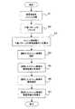
図2は、実施形態の表面段差測定方法を示すフローチャートであり、次にこの図の各ステップS1〜S7の順に従って、その他の図を参照しつつ実施形態の表面段差測定方法を説明する。<Surface step measurement method>
FIG. 2 is a flowchart showing the surface level difference measuring method according to the embodiment. Next, the surface level difference measuring method according to the embodiment will be described according to the order of steps S1 to S7 in this figure with reference to other figures.
先ず、ステップS1では、表面段差を測定する検査体における測定領域をメッシュ分割する。ここでは、図3に示すように、半導体ウェハからなる検査体1に設けられた複数チップのうちの所定のチップ領域を測定領域6とする。そして、図中矢印で引き出した拡大図に示すように、この測定領域6をメッシュ分割する。図示した例においては、2mm×2mmの測定領域(チップ領域)6を、0.1mm×0.1mmの各メッシュ領域7,7,…に400分割する。 First, in step S1, the measurement region in the inspection object for measuring the surface level difference is divided into meshes. Here, as shown in FIG. 3, a predetermined chip region of a plurality of chips provided on the
次に、ステップS2では、検査体における下地パターンのリサイズを行う。ここでは、図4に示すように、下地パターン3の平面形状を全周方向に拡大するようにリサイズを行う。この際、平坦化処理前における平坦化膜(つまり図1に示した材料膜4a)の成膜膜厚tの分だけ、下地パターン3の平面形状を全周方向に拡大する。例えば、平坦化膜(材料膜)の成膜膜厚t=450nmであれば、下地パターン3の平面形状を全周方向に450nm分だけ拡大する。 Next, in step S2, the base pattern on the inspection body is resized. Here, as shown in FIG. 4, resizing is performed so that the planar shape of the
また、このリサイズによって拡大した複数の下地パターン3a同士が重なりを持つ場合には、これらの重なりを持った複数の下地パターン3a,3aを1つの下地パターン3aとする処理を行うこととする。 In addition, when a plurality of
以上のような下地パターン3のリサイズは、下地パターン3の設計データ、例えば下地パターン形成で用いた露光マスクのマスクデータに対して演算処理を加えることで行われる。 The resize of the
尚、図面においては、1つのメッシュ領域7のみを図示したが、このリサイズは測定領域6内に配置される全ての下地パターン3に対して実行される。また、以上のステップS1とステップS2とは、逆の順に実行しても良く、平行して実行しても良い。 Although only one
そして、以上のステップS1およびステップS2が終了した後のステップS3では、ステップS1でメッシュ分割した各メッシュ領域について、ステップS2でリサイズした下地パターン3aの専有面積率σを算出する。ここでは、図5に示すように、各メッシュ領域7の面積(0.1mm×0.1mm)に占める、下地パターン3aの総面積S(3a)の割合を専有面積率σとして算出する。これは、測定領域における全てのメッシュ領域7で同様に行う。この際、先のステップS2においてリサイズした下地パターン3aの専有面積率σを算出するようにしたことで、平坦化処理に与える影響をより正確に数値化した値として専有面積率σの算出を行うことができる。 Then, in step S3 after step S1 and step S2 are completed, the exclusive area ratio σ of the
次いで、ステップS4では、ステップS3で算出された各メッシュ領域7の専有面積率σに基づき、表面段差分布を測定するメッシュ領域を選択する。ここでは、図6に示すように、専有面積率σの高い側から所定数分の高密度メッシュ領域7a,7a,…、および専有面積率σの低い側から所定数分の低密度メッシュ領域7b,7b,…とを選択する。 Next, in step S4, based on the exclusive area ratio σ of each
この際、例えば専有面積率σの高い側から所定割合(例えば上位20%)の数の高密度メッシュ領域7a,7a,…と、専有面積率σの低い側から所定割合(例えば下位20%)の数の低密度メッシュ領域7b,7b,…を選択するようにしても良い。この場合、全メッシュ領域7が400個であるとすると、高密度メッシュ領域7aとして40箇所、低密度メッシュ領域7bとして40箇所のメッシュ領域がそれぞれ選択される。また、専有面積率σが所定値以上(例えば80%以上)の高密度メッシュ領域7a,7a,…と、専有面積率σが所定値以下(例えば25%以下)の高密度メッシュ領域7b,7b,…とを選択するようにしても良い。ただしこの場合、高密度メッシュ領域7aと低密度メッシュ領域7bとが、それぞれ1つ以上選択されるように設定する。 In this case, for example, a predetermined ratio (for example, the upper 20%) of the high
その後、ステップS5では、先のステップS4で選択した各メッシュ領域7a,…,7b,…の表面段差分布を測定する。ここでは、例えばAFMを用い、選択した各メッシュ領域7a,…,7b,…の全面をスキャニング測定し、それぞれの領域における表面段差分布を測定する。この際、表面段差分布の測定精度(解像度)を上げるためには、x方向へのスキャニング測定をy方向にずらす間隔を狭くし、1つのメッシュ領域におけるスキャニング測定の本数を増加させる。尚、測定機器の一例として用いられるAFMによる表面段差分布の測定の詳細については、表面段差測定装置の構成として以降に詳細に説明する。 Thereafter, in step S5, the surface level difference distribution of each
また、ステップS6では、選択された先のステップS4で選択されたメッシュ領域7a,…,7b,…のそれぞれにおいて、平坦化膜の膜厚を測定する。ここでは、図1に示すように、下地パターン3の下部における基板2上の平坦化膜4の膜厚t1を、各メッシュ領域7a,…,7b,…の1箇所で測定する。この際、例えばエリプソメータを用いた膜厚測定を行う。 In step S6, the film thickness of the planarizing film is measured in each of the
尚、以上のステプS5とステップS6とは、逆の順に実行しても良く、平行して実行しても良い。 The above step S5 and step S6 may be executed in the reverse order or may be executed in parallel.
そして、以上のステップS5およびステップS6を行った後のステップS7では、ステップS5で測定した各メッシュ領域7a,…,7b,…の表面段差分布を、ステップS6で測定した各メッシュ領域7a,…,7b,…における平坦化膜の膜厚t1に基づいて補正する。この際、各メッシュ領域7a,…,7b,…が分散配置されることで生じる表面段差分布の測定ばらつき(測定機器による測定ばらつき)を、各メッシュ領域7a,…,7b,…で測定された平坦化膜の膜厚t1の差に基づいて補正する。 Then, in step S7 after performing the above steps S5 and S6, the surface step distribution of each
以上により得られた各メッシュ領域7a,…,7b,…の表面段差分布を、測定領域6の中の全体を代表する表面段差分布とする。また必要に応じて、得られた表面段差分布から、例えば精度良好に測定領域における段差ばらつき(例えば凸部と凹部の最大差)を得る。 The surface step distribution of each
尚、各メッシュ領域7a,…,7b,…が測定領域6内に分散配置されることで生じる表面段差分布の測定ばらつき(測定機器による測定ばらつき)を考慮する必要のない場合には、ステップS6,S7を行う必要はない。 If it is not necessary to take into account the measurement variation of the surface step distribution (measurement variation due to the measuring device) caused by the
以上説明した表面段差測定方法によれば、測定領域6を分割した各メッシュ領域7のうちから選択された高密度メッシュ領域7a,7a,…と低密度メッシュ領域7b,7b,…とについてのみ、表面段差分布を測定する構成である。これらの選択されたメッシュ領域7a,…,7b,…のうち、高密度メッシュ領域7a,7a,…は、下地パターン3の専有面積率が高い領域であるため、平坦化膜4に施されるCMPのような平坦化処理が進み難く表面位置が高めになる。一方、低密度メッシュ領域7b,7b,…は、下地パターン3の専有面積率が低い領域であるため、平坦化処理が進み易く表面位置が低めになる。 According to the surface level difference measuring method described above, only the high
このため、測定領域6の全領域について表面段差分布を測定することなく、平坦化表面Aにおける最も高い位置部分と平坦化表面Aにおける最も低い位置部分とを確実に含む領域で、表面段差分布の測定が成されることになる。したがって、これらの選択されたメッシュ領域7a,…,7b,…について、高解像度で表面段差分布を測定することで、測定時間を大幅に削減しつつも、精度良好に測定領域における表面段差(凸部と凹部の最大差)を得ることができる。 For this reason, the surface level difference distribution of the entire region of the
これにより、表面段差の測定において、測定精度を確保しつつも、大幅にスループットの向上を図ることが可能になる。またこの結果、半導体プロセスの開発時間の短縮を図り、半導体プロセス技術の向上を図ることができる。そして特に、ゲート線幅65nm世代以降の半導体プロセス開発においては、本発明の表面段差測定方法による測定時間の削減が必要不可欠となる。 Thereby, in the measurement of the surface level difference, it is possible to greatly improve the throughput while ensuring the measurement accuracy. As a result, the development time of the semiconductor process can be shortened and the semiconductor process technology can be improved. In particular, in the development of a semiconductor process with a gate line width of 65 nm or later, it is indispensable to reduce the measuring time by the surface step measuring method of the present invention.
<表面段差測定装置>
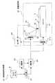
図7は、実施形態の表面段差測定装置の構成図である。以下、この図7と先の図2のフローチャートに基づいて、本実施形態の表面段差測定装置の構成を説明する。<Surface level difference measuring device>
FIG. 7 is a configuration diagram of the surface level difference measuring apparatus according to the embodiment. Hereinafter, the configuration of the surface level difference measuring apparatus according to the present embodiment will be described with reference to FIG. 7 and the flowchart of FIG.
この図に示す表面段差測定装置20は、先に図1〜図6を用いて説明した表面段差測定方法を実行するための装置であり、入力部21、演算部23、選択部25、段差測定部27、および出力部29を備えている。 A surface level difference measuring apparatus 20 shown in this figure is an apparatus for executing the surface level difference measuring method described above with reference to FIGS. 1 to 6, and includes an
このうち、入力部21は、上述した表面段差測定方法に必要な下地パターンに関する設計データ(マスクデータD)、測定条件などの情報を入力する部分である。この入力部21から入力される測定条件としては、ステップS1で行うメッシュ分割の分割数や、ステップS2で行う下地パターンのリサイズの量(平坦化膜の成膜膜厚t)や、さらにはステップS4で行うメッシュ領域の選択条件等である。 Among these, the
そして、演算部23は、入力部21から入力された情報に基づいて、上述したステップS1からステップS3までを行う部分である。すなわち、この演算部23では、入力部21から入力された情報に基づいて、表面段差測定方法の平坦化表面における測定領域内を所定面積にメッシュ分割してなるメッシュ領域毎に下地パターンの専有面積率σを算出するまでを行う。 And the calculating
また、選択部25は、入力部21から入力された情報と、演算部23で算出された各メッシュ領域における下地パターンの専有面積率σとに基づき、上述したステップS4を行う部分である。このため、この選択部25では、入力部21から入力された情報と、演算部23で算出された専有面積率σとに基づき、次に説明する段差測定部27において表面段差分布の測定を行うメッシュ領域を選択する。 The
そして段差測定部27は、上述したステップS5を測定する部分であり、選択部25で選択されたメッシュ領域のみについて表面段差分布を測定する。 The level difference measuring unit 27 measures the above-described step S5, and measures the surface level difference distribution only for the mesh region selected by the
この段差測定部27は、例えばAFMであり、図1に示した測定対象である検査体(半導体ウェハ)1を載置するステージ31を備えている。このステージ31には、ステージ31を水平面内においてX−Y方向に駆動する駆動部31aが備えられている。 The step measurement unit 27 is, for example, an AFM, and includes a
そして、ステージ31上には、このステージ31上に載置保持された検査体1の平坦化表面Aにおいて自在にスキャニングされる探針32が設けられている。この探針32は、平坦化表面Aと探針63との間に掛かる力が数nmNの一定に制御される。 On the
また、探針32の上端にはカンチレバー33が接続されている。このカンチレバー33の上方には、カンチレバー33にレーザ光を照射するレーザ発信器34と、カンチレバー33で反射したレーザ光を検出する光学顕微鏡35とが設けられている。これらのレーザ発信器34と光学顕微鏡35とは、平坦化表面Aにおいて探針32をスキャンさせることで、平坦化表面Aの表面段差によってカンチレバー33が変位した場合、この変位量がレーザ光の検出によって連続的に測定される構成となっている。そして、これらの探針32、カンチレバー33、レーザ発信器34、光学顕微鏡35には、これらを一体にX−Y方向に駆動する駆動部37が設けられている。 A
各駆動部31a,37には、上述した選択部25が接続されている。これにより、選択部25で選択されたメッシュ領域のみの平坦化表面A上において、探針32がスキャニングされる構成となっている。 The
さらにこれらの駆動部31a,37および光学顕微鏡35は、出力部29に接続されており、駆動部31a,37から得られる測定部の位置と、光学顕微鏡35から得られるカンチレバー33の変位量とを関係づけた情報が、測定されたメッシュ領域における表面段差分布として出力される。また必要に応じて、この出力部29が演算部を有しており、表面段差分布が測定された全てのメッシュ領域のうちの凸部と凹部の最大差を出力させるようにしても良い。 Furthermore, these
またここでの図示は省略したが、以上説明した構成の他にも、選択されたメッシュ領域について前記平坦化膜の膜厚を測定する膜厚測定部と、膜厚測定部で測定された各メッシュ領域の膜厚に基づいて段差測定部27で測定された各メッシュ領域の表面段差分布を補正する補正部とをさらに備えても良い。 Although illustration is omitted here, in addition to the configuration described above, the film thickness measurement unit that measures the film thickness of the planarization film for the selected mesh region, and each of the film thickness measurement units measured by the film thickness measurement unit You may further provide the correction | amendment part which correct | amends the surface level | step difference distribution of each mesh area | region measured by the level | step difference measurement part 27 based on the film thickness of a mesh area | region.
以上説明した構成の表面段差測定装置20は、通常の段差測定機器で構成される段差測定部27に対して、さらに上述したステップS1〜ステップS3を実行する演算部23、およびステップS4を実行する選択部25を設け、この選択部25で選択されたメッシュ領域のみにおいて表面段差分布が測定される構成となっている。したがって、上述したように、測定精度を確保しつつも、大幅にスループットの向上を図ることが可能な表面段差測定を実行することが可能である。 The surface level difference measuring apparatus 20 having the configuration described above further executes the
尚、本発明で表面段差を測定する平坦化膜としては、成膜後に平坦化処理が施されたものに限定されることはない。例えば、フロー性を有する成膜条件で成膜されることで成膜した時点である程度の平坦性を有する膜であっても良い。また、このような平坦性を備えず下地パターンに追従した表面形状を有する膜であっても良い。 Note that the planarization film for measuring the surface level difference in the present invention is not limited to a film that has been planarized after the film formation. For example, a film having a certain degree of flatness may be used when the film is formed under film forming conditions having flow properties. Moreover, the film | membrane which does not have such flatness but has the surface shape which followed the base pattern may be sufficient.
1…基板、3…下地パターン、3a…下地パターン(リサイズ後)、4…平坦化膜、7…メッシュ領域、7a…高密度メッシュ領域、7b…低密度メッシュ領域、20…表面段差測定装置、23…演算部、25…選択部、27…段差測定部、A…平坦化表面 DESCRIPTION OF
Claims (10)
Translated fromJapanese前記平坦化表面における測定領域内を所定面積にメッシュ分割してなるメッシュ領域毎に前記下地パターンの専有面積率を算出し、
前記算出された専有面積率に基づき、専有面積率の高い側から所定数分のメッシュ領域と専有面積率の低い側から所定数分のメッシュ領域とを選択し、
前記選択されたメッシュ領域の表面段差分布のみを測定する
ことを特徴とする表面段差測定方法。A surface level difference measuring method for measuring a level difference of a flattened surface formed by covering the substrate with a leveling film in a state of being embedded between base patterns formed on the substrate,
Calculate the exclusive area ratio of the ground pattern for each mesh region obtained by dividing the measurement region in the planarized surface into a predetermined area,
Based on the calculated exclusive area ratio, select a predetermined number of mesh areas from the high exclusive area ratio side and a predetermined number of mesh areas from the low exclusive area ratio side,
Only the surface level difference distribution of the selected mesh region is measured.
前記下地パターンの専有面積率として、平坦化処理前における前記平坦化膜の成膜膜厚分だけ平面形状を全周方向に拡大するように当該下地パターンをリサイズし、当該リサイズした下地パターンの専有面積率を算出する
ことを特徴とする表面段差測定方法。In the surface level | step difference measuring method of Claim 1,
As the exclusive area ratio of the base pattern, the base pattern is resized so that the planar shape is enlarged in the entire circumferential direction by the film thickness of the planarizing film before the flattening process, and the resized base pattern is exclusively used. A method for measuring a surface level difference, comprising calculating an area ratio.
前記リサイズした複数の下地パターン同士が重なりを持つ場合には、当該複数の下地パターンを1つの下地パターンとして前記専有面積率を算出する
ことを特徴とする表面段差測定方法。In the surface level | step difference measuring method of Claim 2,
When the plurality of resized base patterns overlap each other, the exclusive area ratio is calculated using the plurality of base patterns as one base pattern.
前記下地パターンの専有面積率は、当該下地パターンの設計データに基づいて算出される
ことを特徴とする表面段差測定方法。In the surface level | step difference measuring method of Claim 1,
The surface level difference measuring method, wherein the exclusive area ratio of the base pattern is calculated based on design data of the base pattern.
前記選択されたメッシュ領域について、前記平坦化膜の膜厚を測定し、
前記測定された各メッシュ領域の膜厚に基づいて、当該各メッシュ領域の表面段差分布を補正する
ことをと特徴とする表面段差測定方法。In the surface level | step difference measuring method of Claim 1,
For the selected mesh region, measure the thickness of the planarization film,
Based on the measured film thickness of each mesh region, the surface step distribution of each mesh region is corrected.
前記平坦化表面における測定領域内を所定面積にメッシュ分割してなるメッシュ領域毎に前記下地パターンの専有面積率を算出する演算部と、
前記演算部で算出された専有面積率に基づき、専有面積率の高い側から所定数分のメッシュ領域と専有面積率の低い側から所定数分のメッシュ領域とを選択する選択部と、
前記選択部で選択されたメッシュ領域の表面段差分布のみを測定する段差測定部とを備えた
ことを特徴とする表面段差測定装置。A surface level difference measuring apparatus for measuring a level difference of a flattened surface formed by covering the substrate with a flattened film in a state of being embedded between base patterns formed on the substrate,
A calculation unit that calculates a dedicated area ratio of the ground pattern for each mesh region obtained by dividing the measurement region in the planarized surface into a predetermined area;
Based on the exclusive area ratio calculated by the calculation unit, a selection unit that selects a predetermined number of mesh regions from the side with a high exclusive area rate and a predetermined number of mesh regions from the side with a low exclusive area rate;
A surface level difference measuring device comprising: a level difference measuring unit that measures only the surface level difference distribution of the mesh region selected by the selection unit.
前記演算部では、平坦化処理前における前記平坦化膜の成膜膜厚分だけ平面形状を全周方向に拡大するように当該下地パターンをリサイズし、当該リサイズした下地パターンの専有面積率を、前記下地パターンの専有面積率として算出する
ことを特徴とする表面段差測定装置。In the surface level | step difference measuring apparatus of Claim 6,
In the arithmetic unit, the base pattern is resized so as to enlarge the planar shape in the entire circumferential direction by the film thickness of the flattening film before the flattening process, and the exclusive area ratio of the resized base pattern is The surface level difference measuring device, which is calculated as an area ratio occupied by the base pattern.
前記演算部では、前記リサイズした複数の下地パターン同士が重なりを持つ場合には、当該複数の下地パターンを1つの下地パターンとして前記専有面積率を算出する
ことを特徴とする表面段差測定装置。In the surface level | step difference measuring apparatus of Claim 7,
When the plurality of resized base patterns overlap each other, the arithmetic unit calculates the exclusive area ratio using the plurality of base patterns as one base pattern.
前記演算部では、前記下地パターンの設計データに基づいて当該下地パターンの専有面積率を算出する
ことを特徴とする表面段差測定装置。In the surface level | step difference measuring apparatus of Claim 6,
The surface level difference measuring apparatus characterized in that the calculation unit calculates a dedicated area ratio of the base pattern based on the design data of the base pattern.
前記選択されたメッシュ領域について前記平坦化膜の膜厚を測定する膜厚測定部と、
前記膜厚測定部で測定された前記各メッシュ領域の膜厚に基づいて、前記段差測定部で測定された前記各メッシュ領域の表面段差分布を補正する補正部とをさらに備えた
ことをと特徴とする表面段差測定装置。
In the surface level | step difference measuring apparatus of Claim 6,
A film thickness measurement unit for measuring the film thickness of the planarization film for the selected mesh region;
And a correction unit that corrects the surface step distribution of each mesh region measured by the step measurement unit based on the film thickness of each mesh region measured by the film thickness measurement unit. A surface level difference measuring device.
Priority Applications (1)
| Application Number | Priority Date | Filing Date | Title |
|---|---|---|---|
| JP2004282961AJP2006100456A (en) | 2004-09-29 | 2004-09-29 | Method and apparatus for measuring surface step |
Applications Claiming Priority (1)
| Application Number | Priority Date | Filing Date | Title |
|---|---|---|---|
| JP2004282961AJP2006100456A (en) | 2004-09-29 | 2004-09-29 | Method and apparatus for measuring surface step |
Publications (1)
| Publication Number | Publication Date |
|---|---|
| JP2006100456Atrue JP2006100456A (en) | 2006-04-13 |
Family
ID=36239993
Family Applications (1)
| Application Number | Title | Priority Date | Filing Date |
|---|---|---|---|
| JP2004282961APendingJP2006100456A (en) | 2004-09-29 | 2004-09-29 | Method and apparatus for measuring surface step |
Country Status (1)
| Country | Link |
|---|---|
| JP (1) | JP2006100456A (en) |
Cited By (2)
| Publication number | Priority date | Publication date | Assignee | Title |
|---|---|---|---|---|
| JP2013520422A (en)* | 2010-02-18 | 2013-06-06 | アンパック バイオ−メディカル サイエンス カンパニー リミテッド | Microdevice manufacturing method |
| JP7545001B2 (en) | 2020-06-01 | 2024-09-03 | 株式会社日立ハイテクサイエンス | Microscope system and method for observing a sample using the microscope system |
- 2004
- 2004-09-29JPJP2004282961Apatent/JP2006100456A/enactivePending
Cited By (3)
| Publication number | Priority date | Publication date | Assignee | Title |
|---|---|---|---|---|
| JP2013520422A (en)* | 2010-02-18 | 2013-06-06 | アンパック バイオ−メディカル サイエンス カンパニー リミテッド | Microdevice manufacturing method |
| US9487394B2 (en) | 2010-02-18 | 2016-11-08 | Shanghai Xinshenpai Technology Co., Ltd. | Methods for fabricating micro-devices |
| JP7545001B2 (en) | 2020-06-01 | 2024-09-03 | 株式会社日立ハイテクサイエンス | Microscope system and method for observing a sample using the microscope system |
Similar Documents
| Publication | Publication Date | Title |
|---|---|---|
| US10249523B2 (en) | Overlay and semiconductor process control using a wafer geometry metric | |
| JP4990548B2 (en) | Manufacturing method of semiconductor device | |
| US7720632B2 (en) | Dimension measuring apparatus and dimension measuring method for semiconductor device | |
| KR102532467B1 (en) | Method for producing a mask for the extreme ultraviolet wavelength range, mask and device | |
| TWI493373B (en) | Method for manufacturing integrated circuit design layout, integrated circuit design layout, and method for positioning pattern in integrated circuit layout | |
| JP2017122716A (en) | System and method for characterizing process guided wafer shapes for process control using CGS interferometry | |
| JP6570010B2 (en) | Method, system, and computer program product for generating a high-density registration map for a mask | |
| KR20210028091A (en) | Method for semiconductor wafer inspection and system thereof | |
| KR20170091721A (en) | Predicting and controlling critical dimension issues and pattern defectivity in wafers using interferometry | |
| US20060160037A1 (en) | Automated sub-field blading for leveling optimization in lithography exposure tool | |
| JP2008098588A (en) | Method of extracting hot spot in layout designing/verification of semiconductor device | |
| JP2006100456A (en) | Method and apparatus for measuring surface step | |
| CN112213922B (en) | Method for setting photoetching exposure conditions | |
| CN109917615A (en) | Method for generating photomask using optical proximity correction model | |
| US6806098B2 (en) | Method and device for assessing surface uniformity of semiconductor device treated by CMP | |
| TW202407742A (en) | 3d volume inspection of semiconductor wafers with increased throughput and accuracy | |
| US11776112B2 (en) | Misalignment measuring apparatus and misalignment measuring method | |
| JP2006100619A (en) | Semiconductor device and manufacturing method therefor | |
| JP2006098150A (en) | Surface level difference measuring method and surface level difference measuring device | |
| JP2006318955A (en) | Pattern dimension measuring method and apparatus | |
| US8014587B2 (en) | Pattern test method of testing, in only specific region, defect of pattern on sample formed by charged beam lithography apparatus | |
| JP2004273962A (en) | Method for designing and method for manufacturing thin film device, and semiconductor manufacturing apparatus | |
| JP4131728B2 (en) | Image creation method, image creation apparatus, and pattern inspection apparatus | |
| CN100481317C (en) | Sample structure of scanning electron microscope made by IC and manufacturing method thereof | |
| KR100687398B1 (en) | Overlay Measurement Method for Semiconductor Devices |