JP2006093588A - Identifying method of semiconductor device and semiconductor package having protruding portion on surface - Google Patents
Identifying method of semiconductor device and semiconductor package having protruding portion on surfaceDownload PDFInfo
- Publication number
- JP2006093588A JP2006093588AJP2004279821AJP2004279821AJP2006093588AJP 2006093588 AJP2006093588 AJP 2006093588AJP 2004279821 AJP2004279821 AJP 2004279821AJP 2004279821 AJP2004279821 AJP 2004279821AJP 2006093588 AJP2006093588 AJP 2006093588A
- Authority
- JP
- Japan
- Prior art keywords
- semiconductor device
- package
- protrusion
- identifying
- shape
- Prior art date
- Legal status (The legal status is an assumption and is not a legal conclusion. Google has not performed a legal analysis and makes no representation as to the accuracy of the status listed.)
- Pending
Links
- 239000004065semiconductorSubstances0.000titleclaimsabstractdescription73
- 238000000034methodMethods0.000titleclaimsabstractdescription28
- 238000012545processingMethods0.000claimsdescription44
- 238000004519manufacturing processMethods0.000claimsdescription5
- 238000007789sealingMethods0.000description21
- 239000011347resinSubstances0.000description8
- 229920005989resinPolymers0.000description8
- 239000003990capacitorSubstances0.000description5
- 229910002056binary alloyInorganic materials0.000description2
- 238000005516engineering processMethods0.000description2
- 239000002184metalSubstances0.000description2
- 230000037303wrinklesEffects0.000description2
- 238000011109contaminationMethods0.000description1
- 238000007796conventional methodMethods0.000description1
- 238000010586diagramMethods0.000description1
- 238000007599dischargingMethods0.000description1
- 230000010365information processingEffects0.000description1
- 238000011835investigationMethods0.000description1
- 239000007787solidSubstances0.000description1
- 230000006641stabilisationEffects0.000description1
- 238000011105stabilizationMethods0.000description1
- 239000000758substrateSubstances0.000description1
- 229920001187thermosetting polymerPolymers0.000description1
- 238000012546transferMethods0.000description1
Images


Classifications
- H—ELECTRICITY
- H01—ELECTRIC ELEMENTS
- H01L—SEMICONDUCTOR DEVICES NOT COVERED BY CLASS H10
- H01L23/00—Details of semiconductor or other solid state devices
- H01L23/544—Marks applied to semiconductor devices or parts, e.g. registration marks, alignment structures, wafer maps
- H—ELECTRICITY
- H01—ELECTRIC ELEMENTS
- H01L—SEMICONDUCTOR DEVICES NOT COVERED BY CLASS H10
- H01L21/00—Processes or apparatus adapted for the manufacture or treatment of semiconductor or solid state devices or of parts thereof
- H01L21/02—Manufacture or treatment of semiconductor devices or of parts thereof
- H01L21/04—Manufacture or treatment of semiconductor devices or of parts thereof the devices having potential barriers, e.g. a PN junction, depletion layer or carrier concentration layer
- H01L21/50—Assembly of semiconductor devices using processes or apparatus not provided for in a single one of the groups H01L21/18 - H01L21/326 or H10D48/04 - H10D48/07 e.g. sealing of a cap to a base of a container
- H01L21/56—Encapsulations, e.g. encapsulation layers, coatings
- H01L21/565—Moulds
- H—ELECTRICITY
- H01—ELECTRIC ELEMENTS
- H01L—SEMICONDUCTOR DEVICES NOT COVERED BY CLASS H10
- H01L23/00—Details of semiconductor or other solid state devices
- H01L23/28—Encapsulations, e.g. encapsulating layers, coatings, e.g. for protection
- H01L23/31—Encapsulations, e.g. encapsulating layers, coatings, e.g. for protection characterised by the arrangement or shape
- H01L23/3107—Encapsulations, e.g. encapsulating layers, coatings, e.g. for protection characterised by the arrangement or shape the device being completely enclosed
- H—ELECTRICITY
- H01—ELECTRIC ELEMENTS
- H01L—SEMICONDUCTOR DEVICES NOT COVERED BY CLASS H10
- H01L2223/00—Details relating to semiconductor or other solid state devices covered by the group H01L23/00
- H01L2223/544—Marks applied to semiconductor devices or parts
- H01L2223/54413—Marks applied to semiconductor devices or parts comprising digital information, e.g. bar codes, data matrix
- H—ELECTRICITY
- H01—ELECTRIC ELEMENTS
- H01L—SEMICONDUCTOR DEVICES NOT COVERED BY CLASS H10
- H01L2223/00—Details relating to semiconductor or other solid state devices covered by the group H01L23/00
- H01L2223/544—Marks applied to semiconductor devices or parts
- H01L2223/5442—Marks applied to semiconductor devices or parts comprising non digital, non alphanumeric information, e.g. symbols
- H—ELECTRICITY
- H01—ELECTRIC ELEMENTS
- H01L—SEMICONDUCTOR DEVICES NOT COVERED BY CLASS H10
- H01L2223/00—Details relating to semiconductor or other solid state devices covered by the group H01L23/00
- H01L2223/544—Marks applied to semiconductor devices or parts
- H01L2223/54473—Marks applied to semiconductor devices or parts for use after dicing
- H01L2223/54486—Located on package parts, e.g. encapsulation, leads, package substrate
- H—ELECTRICITY
- H01—ELECTRIC ELEMENTS
- H01L—SEMICONDUCTOR DEVICES NOT COVERED BY CLASS H10
- H01L2924/00—Indexing scheme for arrangements or methods for connecting or disconnecting semiconductor or solid-state bodies as covered by H01L24/00
- H01L2924/0001—Technical content checked by a classifier
- H01L2924/0002—Not covered by any one of groups H01L24/00, H01L24/00 and H01L2224/00
- H—ELECTRICITY
- H01—ELECTRIC ELEMENTS
- H01L—SEMICONDUCTOR DEVICES NOT COVERED BY CLASS H10
- H01L2924/00—Indexing scheme for arrangements or methods for connecting or disconnecting semiconductor or solid-state bodies as covered by H01L24/00
- H01L2924/15—Details of package parts other than the semiconductor or other solid state devices to be connected
- H01L2924/181—Encapsulation
- H01L2924/1815—Shape
- H—ELECTRICITY
- H01—ELECTRIC ELEMENTS
- H01L—SEMICONDUCTOR DEVICES NOT COVERED BY CLASS H10
- H01L2924/00—Indexing scheme for arrangements or methods for connecting or disconnecting semiconductor or solid-state bodies as covered by H01L24/00
- H01L2924/19—Details of hybrid assemblies other than the semiconductor or other solid state devices to be connected
- H01L2924/1901—Structure
- H01L2924/1904—Component type
- H01L2924/19041—Component type being a capacitor
Landscapes
- Engineering & Computer Science (AREA)
- Physics & Mathematics (AREA)
- Condensed Matter Physics & Semiconductors (AREA)
- General Physics & Mathematics (AREA)
- Computer Hardware Design (AREA)
- Microelectronics & Electronic Packaging (AREA)
- Power Engineering (AREA)
- Manufacturing & Machinery (AREA)
- Structures Or Materials For Encapsulating Or Coating Semiconductor Devices Or Solid State Devices (AREA)
- Encapsulation Of And Coatings For Semiconductor Or Solid State Devices (AREA)
Abstract
Description
Translated fromJapanese本発明は、表面に突起部を有する半導体装置および半導体パッケージの識別方法に関する。 The present invention relates to a semiconductor device having a protrusion on the surface and a method for identifying a semiconductor package.
従来のパッケージ表面に突起を有する半導体装置としては、例えば特許文献1に記載されたものがある。同文献に記載された半導体装置を図9に示す。 As a conventional semiconductor device having a protrusion on the surface of a package, for example, there is one described in
この半導体装置において、先端面に、深さ約0.05mmで、文字、マ−クの刻印が施されたエジェクタピン5は、その先端面が下金型4の底面から0.05〜0.1mm突き出るように設定されている。コンデンサ本体1を電極引出し部2に接合し、その電極引出し部2を下金型4に位置決めし、上金型3により挟みこみ、コンデンサ本体1を密閉する。密閉されたコンデンサ本体1の周囲の空間6に樹脂を加圧注入し、金型内で硬化させ、文字及びマ−クを刻印したモ−ルド外装積層フイルムコンデンサを形成する。エジェクタピン5の先端面に文字及びマ−ク等の刻印が施された封止金型を用いて電子部品を封止することで、完成された製品の状態で、どのキャビティで封止された製品かを知り、製品の品質を追跡できるようになっている。 In this semiconductor device, the tip of the ejector pin 5 having a depth of about 0.05 mm and engraved characters and marks on the front end surface is 0.05 to 0. 0 mm from the bottom surface of the lower mold 4. It is set to protrude 1 mm. The capacitor
しかしながら、上記半導体装置の製造工程における連続加工において、その1個1個について、加工条件を変更する必要が生じることがある。 However, in the continuous processing in the manufacturing process of the semiconductor device, it may be necessary to change the processing conditions for each one.
そのうち、半導体装置の封止工程以降の後工程における加工において、封止金型内の複数キャビティの1個毎に後工程の加工条件を変える必要がある場合には、連続作業のなかで、個々の半導体装置のキャビティ刻印など、個々のキャビティを特定できる部分を読み取って、すぐに加工条件を変更することが求められる。そのために、キャビティ刻印を読み取ることが必要になるが、誤認識してしまうと、間違った加工をしてしまうので、刻印読取の精度を上げる必要がある。したがって、画像処理装置などの自動認識装置を用いる必要がある。 Among them, in the processing in the subsequent process after the sealing process of the semiconductor device, if it is necessary to change the processing conditions in the subsequent process for each of the plurality of cavities in the sealing mold, It is required to immediately change the processing conditions by reading a part where each cavity can be specified, such as cavity marking of the semiconductor device. For this reason, it is necessary to read the cavity stamp, but if it is misrecognized, it will be processed incorrectly, so that it is necessary to increase the accuracy of the stamp reading. Therefore, it is necessary to use an automatic recognition device such as an image processing device.
また、従来の技術におけるキャビティ刻印は、人間の目による調査のために設けられていたので、読み取ることができればよく、文字やマークの刻印とされていた。そのため、キズや汚れがあると、画像処理装置などの自動認識装置が違う文字として読み取ってしまう、いわゆる誤認識を起こしてしまい、間違った加工をしてしまうことがあった。 In addition, since the cavity stamp in the conventional technique is provided for the investigation by the human eye, it is sufficient that it can be read, and it has been used as a stamp of characters and marks. For this reason, if there are scratches or dirt, an automatic recognition device such as an image processing device may read as a different character, so-called misrecognition, resulting in incorrect processing.
上述の誤認識が発生するメカニズムは以下の通りである。 The mechanism by which the above-described misrecognition occurs is as follows.
文字やマークの刻印の場合、同色であるために、画像処理装置は、その立体形状を光で反射させることで認識する方法をとる。この場合、キズや汚れがあると、刻印以外にキズや汚れも光を反射して、画像処理装置に映る。そして、文字、マークの形状に余計な線分が入ったり、途切れたりした画像データをとりこんでしまう。その結果、別の文字として認識してしまい、誤認識が発生することがあった。 In the case of imprinting of characters and marks, since they are the same color, the image processing apparatus takes a method of recognizing the solid shape by reflecting it with light. In this case, if there is a flaw or dirt, the flaw or dirt in addition to the stamp reflects light and is reflected on the image processing apparatus. Then, image data that includes extra line segments or breaks in the shape of characters and marks is captured. As a result, it may be recognized as another character, and erroneous recognition may occur.
たとえば、図10(a)のように、アルファベットの「O」が途切れて、図10(b)のような形状になると、画像処理装置がアルファベットの「C」と誤認識することがあった。また、たとえば、図10(c)のようにアルファベットの「I」に横線状のキズが入って、図10(d)のような形状になると、画像処理装置が「J」と誤認識することがあった。 For example, as illustrated in FIG. 10A, when the alphabet “O” is interrupted and the shape is as illustrated in FIG. 10B, the image processing apparatus may erroneously recognize the alphabet “C”. Further, for example, if the alphabet “I” has a horizontal line-like scratch as shown in FIG. 10C and the shape as shown in FIG. 10D is obtained, the image processing apparatus erroneously recognizes “J”. was there.
本発明は上記事情に鑑みてなされたものであり、半導体装置を正確に認識して、当該半導体装置のパッケージの種別を特定する技術を提供する。 The present invention has been made in view of the above circumstances, and provides a technique for accurately recognizing a semiconductor device and specifying the type of package of the semiconductor device.
本発明によれば、半導体装置であって、前記半導体装置の表面に突起部が形成される領域が設けられ、前記領域内の前記突起部の有無を識別することにより当該半導体装置のパッケージの種別を特定できるように構成された半導体装置が提供される。 According to the present invention, a semiconductor device is provided with a region where a protrusion is formed on the surface of the semiconductor device, and by identifying the presence or absence of the protrusion in the region, the type of the package of the semiconductor device A semiconductor device configured to be able to specify is provided.
この発明に係る半導体装置は、表面に突起部が形成される領域が設けられた半導体装置である。そのため、上記突起部の有無を識別することによって、半導体装置を正確に認識して、当該半導体装置のパッケージの種別を特定する技術を提供することができる。 The semiconductor device according to the present invention is a semiconductor device provided with a region where a protrusion is formed on the surface. Therefore, by identifying the presence or absence of the protruding portion, it is possible to provide a technology for accurately recognizing the semiconductor device and specifying the package type of the semiconductor device.
本発明によれば、半導体パッケージの識別方法であって、半導体装置表面の所定の領域の画像情報を画像処理装置に取り込む工程と、前記画像処理装置において、前記画像情報から前記所定の領域の突起部の有無を判定する工程と、前記判定結果に基づいて、半導体パッケージの識別を行う工程と、を含むことを特徴とする半導体パッケージの識別方法が提供される。 According to the present invention, there is provided a method for identifying a semiconductor package, the step of capturing image information of a predetermined area on the surface of a semiconductor device into an image processing apparatus, and a protrusion of the predetermined area from the image information in the image processing apparatus. There is provided a method for identifying a semiconductor package, comprising: a step of determining presence / absence of a portion; and a step of identifying a semiconductor package based on the determination result.
この発明によれば、半導体装置表面の画像情報が取り込まれた画像処理装置において所定の領域の突起部の有無を判定し、その判定結果に基づいて半導体パッケージの識別を行うことができる。そのため、半導体装置を正確に認識して、当該半導体装置のパッケージの種別を特定する技術を提供することができる。 According to the present invention, it is possible to determine the presence / absence of a protrusion in a predetermined region in an image processing apparatus in which image information on the surface of a semiconductor device is captured, and to identify a semiconductor package based on the determination result. Therefore, it is possible to provide a technique for accurately recognizing a semiconductor device and specifying the type of package of the semiconductor device.
本発明によれば、半導体装置の表面に突起部が形成される領域を設け、上記突起部の有無を判別することによって、半導体装置を正確に認識して、当該半導体装置のパッケージの種別を特定する技術が提供される。 According to the present invention, by providing a region where a protrusion is formed on the surface of a semiconductor device, and determining the presence or absence of the protrusion, the semiconductor device is accurately recognized and the package type of the semiconductor device is specified. Technology is provided.
以下、本発明の実施の形態について、図面を用いて説明する。尚、すべての図面において、同様な構成要素には同様の符号を付し、適宜説明を省略する。 Hereinafter, embodiments of the present invention will be described with reference to the drawings. In all the drawings, the same reference numerals are given to the same components, and the description will be omitted as appropriate.
第1の実施の形態
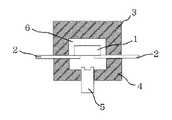
本実施形態の封止金型100の構成図を図1に示す。ここで、封止金型100は、後述するパッケージ20を製造する工程において用いられる。1st Embodiment The block diagram of the sealing metal mold | die 100 of this embodiment is shown in FIG. Here, the sealing
上金型9および下金型10が組み合わされることで、空間12が形成される。 A
チップ7は、空間12内に置かれ、後述する封止樹脂19により封止される。チップ7としては、たとえば半導体チップが用いられる。 The
リード8は、チップ7を載置する基板であり、リードフレームの一部分をなす。 The
エジェクタピン11は、パッケージの製造工程において、チップ7が封止樹脂19により封止された後に、上金型9および下金型10からパッケージ20を排出させるために封止金型100に設けられる。先端面に丸形状の刻印(突起)が施されたエジェクタピン11は、先端面が下金型10の底面から0.05〜0.3mm突き出るよう設定されている。 The
封止樹脂19としては、たとえば、熱硬化性樹脂などが用いられる。 As the
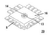
封止金型100を用いて封止されたチップ7のパッケージ20の外観を図2に示す。 An appearance of the
チップ7(図1)はリード8に接合され、リード8は下金型10(図1)に位置決めされ、上金型9(図1)により挟み込まれ、チップ7が密閉される。密閉されたチップ7の周囲の空間12に封止樹脂19が注入・硬化され、先端面に刻印を備えるエジェクタピン11により、封止金型100から排出されることで、表面に丸形状が刻印されたパッケージ20となる。このとき、エジェクタピン部13は、円状のくぼみとなり、刻印部14は丸形状の突起部となる。 The chip 7 (FIG. 1) is joined to the
刻印部14は、たとえば、直径1mm程度の丸形状の集合体であり、所定の箇所に丸形状の突起部が設けられている。刻印部14のそれぞれの部分は、キャビティ毎に規則性を有しており、各部分には、パッケージの種別によって、突起が設けられたり、設けられなかったりする。つまり、刻印部14は、複数のサブエリアである丸形状の突起部が設けられる領域であり、丸形状の突起部は、パッケージの種別に応じて、上記領域内の特定位置に設けられる。本実施形態においては、上記4ヶ所の位置をそれぞれ4ビット、3ビット、2ビット、1ビットと割り付けてあり、封止金型内の各キャビティナンバーが2進法に変換されて、「1」のビットの位置には丸形状の突起が設けられ、「0」のビットの位置には丸形状の突起が設けられないといった規則性を有する。4個の丸形状の「有り」、「無し」の組み合わせは、1つのキャビティにおいては、1つの組み合わせしかないようにする。 The marking
図3に示すようにパッケージ表面を押し出す側のエジェクタピンに刻印をつけることでパッケージ20の表面側に丸形状を設けることもできるし、キャビティを構成する金型の内側の面に刻印(突起)を設けることによって、図4に示すように、パッケージ20の表面側のエジェクタピン部13以外の場所に丸形状を設けることもできる。 As shown in FIG. 3, it is possible to provide a round shape on the surface side of the
以下に、丸形状の突起部の読み取り方法の一例を示す。 Below, an example of the reading method of a round-shaped projection part is shown.
図5に、形状読み取り装置の構成を示す。 FIG. 5 shows the configuration of the shape reading device.
まず、カメラ16を用いて、パッケージ20の表面の所定の領域の画像情報を画像処理装置17に取り込む。画像処理装置17は、パッケージ20の表面の決められた丸形状の突起部の位置に、それぞれウインドウ15を設ける。すなわち、複数のサブエリアのそれぞれにウインドウ15を設ける。画像処理装置17においては、個々のウインドウ15内に映る丸形状の突起部の有無をそれぞれ判定する処理が行なわれる。 First, using the
次に、各ウインドウ15内に丸形状の突起部がある場合は「1」を、ない場合は「0」と、画像処理装置17における判定結果を2進数に変換して加工装置18に転送する。このとき、各ウインドウ15を順番に4ビット、3ビット、2ビット、1ビットと位置付けしておく。画像処理装置17から、丸形状の突起部の有無の情報が、4ビットの「1」「0」の2進法の情報として加工装置18に転送されるので、加工装置18に設けられたコンピュータでは、そのまま、2進数に変換された情報に基づいてパッケージ20の識別を行うことができる。 Next, if there is a round-shaped protrusion in each
図5に示すように、キャビティが11番のとき、2進法では「1011」となる。各ビットで「1」に対応するウインドウには丸形状の突起部があり、「0」に対応するウインドウには丸形状の突起部がないとすると、画像処理装置17は「1011」の情報を読み取り、加工装置18にその情報を転送する。加工装置18に設けられたコンピュータは、「1011」の情報をそのまま用い、10進法の11番の加工条件に変更することができる。 As shown in FIG. 5, when the cavity is No. 11, it is “1011” in the binary system. If the window corresponding to “1” in each bit has a round-shaped protrusion, and the window corresponding to “0” does not have a round-shaped protrusion, the
また、ウインドウの設定方法として、全体を1ウインドウとし、ウインドウ内の幾何学形状の数をカウントする方式でもよいし、基準画像を登録しておこなうパターンマッチングの方法でもよい。ここで、幾何学形状とは、四角形、三角形、星形など丸形状以外の形状でもよいが、「あ」、「C」などの文字は含まれないものとする。 Further, as a window setting method, there may be a method in which the whole is one window and the number of geometric shapes in the window is counted, or a pattern matching method in which a reference image is registered may be used. Here, the geometric shape may be a shape other than a round shape such as a quadrangle, a triangle, or a star, but does not include characters such as “A” and “C”.
以下、本実施形態の効果について説明する。 Hereinafter, the effect of this embodiment will be described.
本実施形態においては、エジェクタピン11を用いてパッケージ表面に設ける形状を丸形状などの幾何学形状とし、画像処理装置では、丸形状の突起部の有無のみを判断する方法を用いることで、当該形状の線が途中で切れたり、瑕疵が生じて新たな線が付加された場合であっても、形状誤認識発生の可能性を低減することができる。たとえば、図6(a)のように、パッケージ表面に丸形状の突起部が設けられているので、図6(b)のように、線が途中で切れたり、図6(c)のように、パッケージ表面に瑕疵が生じて新たな線が付加されたとしても、画像処理装置17においては、丸形状の突起部の有無を読み取るだけである。そのため、丸形状の突起部を「ある」と読み取ることが可能となるからである。したがって、チップ7のパッケージ20の種別を特定することができる。 In the present embodiment, the shape provided on the surface of the package using the ejector pins 11 is a geometric shape such as a round shape, and the image processing apparatus uses a method of determining only the presence or absence of a round-shaped protrusion. Even if the shape line is cut off in the middle or a new line is added due to wrinkles, the possibility of occurrence of shape error recognition can be reduced. For example, as shown in FIG. 6 (a), a round-shaped protrusion is provided on the surface of the package, so that the line may be cut halfway as shown in FIG. 6 (b) or as shown in FIG. 6 (c). Even if wrinkles occur on the package surface and a new line is added, the
また、カメラ15を介して、パッケージ20の表面に設けられた刻印部14の画像情報が取り込まれた画像処理装置17において、刻印部14に設けられた丸形状などの幾何学形状の突起部の有無に関する情報が2進数に変換される。そのため、2進数に変換された情報を加工装置18にリアルタイムに送信することができ、その情報に基づいてコンピューターで刻印部14における丸形状の突起部の有無を判定することができる。そのため、その判定結果に基づいてパッケージ20の識別を正確に行うことができる。 Further, in the
第2の実施の形態
本実施の形態は、エジェクタピンの先端面に設けられた突起の形状がバーコード状になっている点で、第1の実施の形態と異なる。Second Embodiment This embodiment is different from the first embodiment in that the shape of the protrusion provided on the tip surface of the ejector pin is a bar code.
封止金型は、第1の実施の形態と同じものを用いることができる。 The same sealing mold as that in the first embodiment can be used.
図1に示すとおり、先端面にバーコードで刻印を施したエジェクタピン11は、エジェクタピン11の先端面が、下金型10の底面から0.05〜0.3mm程度突き出るように設定されている。チップ7はリード8に接合され、リード8は下金型10に位置決めされ、上金型9を用いて挟みこみ、チップ7が密閉される。密閉されたチップ7の周囲の空間12に封止樹脂19が注入・硬化される。そして、バーコードが刻印されたパッケージ20の外形となる。このときエジェクタピン部13は、円状のくぼみとなり、刻印部14はバーコードの突起(凹凸部)となる。 As shown in FIG. 1, the
一次元バーコードを刻印した場合、図7のような半導体装置外観図(裏面斜視図)となる。 When a one-dimensional barcode is engraved, the semiconductor device external view (back perspective view) as shown in FIG. 7 is obtained.
二次元バーコードを刻印した場合、図8のような半導体装置外観図(裏面斜視図)となる。ここで、第1の実施の形態と同様、表面側のエジェクタピン11に刻印をつけることもできるし、キャビティ自体に刻印をつけることもできる。 When the two-dimensional barcode is engraved, the semiconductor device external view (back perspective view) as shown in FIG. 8 is obtained. Here, as in the first embodiment, the front-
本実施形態に係るバーコード状刻印の場合、たとえば、以下のような方法で形状の読み取りをすることができる。 In the case of the bar code-shaped inscription according to the present embodiment, for example, the shape can be read by the following method.
まず、バーコードリーダでバーコード情報を取り込む。 First, barcode information is captured by a barcode reader.
次に、取り込んだバーコード情報を転送し、加工装置18のコンピュータではそのまま情報処理をおこない、加工条件を変更できる。 Next, the captured bar code information is transferred, and the computer of the
以下、本実施形態の効果について説明する。 Hereinafter, the effect of this embodiment will be described.
バーコードも幾何学形状の集合体であるので、線の途切れ、新たな線、および線の汚れの存在に対して、第1の実施の形態で説明した丸形状の突起部と同様に誤認識発生の抑制効果を発揮することができる。また、バーコードも、線の途切れ、新たな線、および線の汚れに対しての読取安定化対策をとっているので、さらに安定した形状の読み取りをすることができる。 Since the barcode is also an aggregate of geometric shapes, the presence of the discontinuity of the line, the new line, and the contamination of the line is erroneously recognized in the same manner as the round-shaped protrusion described in the first embodiment. The effect of suppressing the generation can be exhibited. In addition, since the bar code is also provided with a reading stabilization measure against line breaks, new lines, and dirt on the lines, it is possible to read a more stable shape.
本実施形態に係るエジェクタピン11に刻印されたバーコードは標準化されているので、特別な読取システムを構築する必要がなく、容易に読み取りを実施することができる。そのため、パッケージの種別を特定することができ、チップ7を封止するために用いられた封止金型100のキャビティナンバーの情報を安定して読み取ることができる。 Since the barcode engraved on the
また、第1の実施の形態と同様、画像処理装置17において、カメラを介して取り込まれた形状に関する情報を2進法の情報として取り出すことで、リアルタイムに加工装置18に送信することができ、そのままコンピュータで処理することができる。 Similarly to the first embodiment, in the
以上、図面を参照して本発明の実施形態について述べたが、これらは本発明の例示であり、上記以外の様々な構成を採用することもできる。 As mentioned above, although embodiment of this invention was described with reference to drawings, these are the illustrations of this invention, Various structures other than the above are also employable.
たとえば、上記実施形態においては、エジェクタピンやキャビティに設けられる突起の形状を、丸形状などの幾何学形状やバーコード形状の刻印としたが、それ以外の形状の刻印やマークであっても、突起を有する形状であり、画像処理装置で正確に認識することができる形状であればよい。 For example, in the above-described embodiment, the shape of the protrusion provided on the ejector pin or the cavity is a geometric shape such as a round shape or an inscription of a barcode shape. Any shape that has a protrusion and can be accurately recognized by the image processing apparatus may be used.
また、上記実施形態においては、チップ7として半導体チップを用いた形態について説明したが、他の能動素子を用いてもよいし、抵抗、コンデンサなどの受動素子を用いてもよい。 In the above embodiment, the semiconductor chip is used as the
また、上記実施形態においては、パッケージ表面に突起部を4ヶ所設けた形態について説明したが、2ヶ所や5ヶ所以上といった複数の突起部が設けられ得る形態でもよいし、1ヶ所に突起部が設けられ得る形態でもよい。 Further, in the above embodiment, the form in which four protrusions are provided on the package surface has been described. However, a form in which a plurality of protrusions such as two places or five or more places may be provided may be provided. The form which can be provided may be sufficient.
7 チップ
8 リード
9 上金型
10 下金型
11 エジェクタピン
12 空間
13 エジェクタピン部
14 刻印部
15 ウインドウ
16 カメラ
17 画像処理装置
18 加工装置
19 封止樹脂
20 パッケージ
100 封止金型7
Claims (14)
Translated fromJapanese前記半導体装置の表面に突起部が形成される領域が設けられ、
前記領域内の前記突起部の有無を識別することにより当該半導体装置のパッケージの種別を特定できるように構成された半導体装置。A semiconductor device,
A region where a protrusion is formed on the surface of the semiconductor device is provided,
A semiconductor device configured to be able to specify a package type of the semiconductor device by identifying the presence or absence of the protrusion in the region.
前記パッケージの製造工程において、金型に設けられたエジェクタピンにより、前記突起部が設けられることを特徴とする半導体装置。The semiconductor device according to claim 1,
In the manufacturing process of the package, the protrusion is provided by an ejector pin provided in a mold.
前記パッケージの製造工程において、金型に設けられた突起により、前記突起部が設けられることを特徴とする半導体装置。The semiconductor device according to claim 1,
In the manufacturing process of the package, the protrusion is provided by a protrusion provided on a mold.
前記突起部は、前記パッケージの種別に応じて、前記領域内の特定位置に設けられることを特徴とする半導体装置。The semiconductor device according to claim 1,
The protrusion is provided at a specific position in the region according to the type of the package.
前記領域は、複数の特定位置を有することを特徴とする半導体装置。The semiconductor device according to claim 1,
The semiconductor device, wherein the region has a plurality of specific positions.
前記突起部の形状は、幾何学形状であることを特徴とする半導体装置。The semiconductor device according to claim 1,
The semiconductor device according to claim 1, wherein the protrusion has a geometric shape.
前記突起部の形状は、バーコード形状であることを特徴とする半導体装置。The semiconductor device according to claim 1,
The semiconductor device according to claim 1, wherein the protrusion has a bar code shape.
前記バーコード形状は、1次元バーコード形状であることを特徴とする半導体装置。The semiconductor device according to claim 7,
The semiconductor device according to claim 1, wherein the barcode shape is a one-dimensional barcode shape.
前記バーコード形状は、2次元バーコード形状であることを特徴とする半導体装置。The semiconductor device according to claim 7,
The semiconductor device according to claim 1, wherein the barcode shape is a two-dimensional barcode shape.
半導体装置表面の所定の領域の画像情報を画像処理装置に取り込む工程と、
前記画像処理装置において、前記画像情報から前記所定の領域の突起部の有無を判定する工程と、
前記判定結果に基づいて、半導体パッケージの識別を行う工程と、
を含むことを特徴とする半導体パッケージの識別方法。A method for identifying a semiconductor package, comprising:
Capturing image information of a predetermined region on the surface of the semiconductor device into the image processing device;
In the image processing apparatus, a step of determining the presence or absence of a protrusion in the predetermined area from the image information;
A step of identifying a semiconductor package based on the determination result;
A method for identifying a semiconductor package, comprising:
前記画像情報を画像処理装置に取り込む工程は、カメラを介して画像情報を画像処理装置に取り込む工程を含むことを特徴とする半導体パッケージの識別方法。The method for identifying a semiconductor package according to claim 10,
The method for identifying a semiconductor package, wherein the step of taking the image information into the image processing device includes a step of taking the image information into the image processing device via a camera.
前記所定の領域は、複数のサブエリアからなり、
前記突起部の有無を判定する工程は、前記複数のサブエリアのそれぞれについて、突起部の有無を判定する工程を含むことを特徴とする半導体パッケージの識別方法。The method of identifying a semiconductor package according to claim 10 or 11,
The predetermined area is composed of a plurality of sub areas.
The step of determining the presence / absence of the protrusion includes a step of determining the presence / absence of a protrusion for each of the plurality of sub-areas.
前記半導体パッケージの識別を行う工程が、
前記画像処理装置において前記判定結果を2進数に変換する工程と、
前記2進数に基づいて半導体パッケージの識別を行う工程と、
を含むことを特徴とする半導体パッケージの識別方法。The method for identifying a semiconductor package according to any one of claims 10 to 12,
The step of identifying the semiconductor package comprises:
Converting the determination result into a binary number in the image processing apparatus;
Identifying a semiconductor package based on the binary number;
A method for identifying a semiconductor package, comprising:
前記画像情報が、バーコード情報であることを特徴とする半導体パッケージの識別方法。The method for identifying a semiconductor package according to claim 10,
A method of identifying a semiconductor package, wherein the image information is barcode information.
Priority Applications (2)
| Application Number | Priority Date | Filing Date | Title |
|---|---|---|---|
| JP2004279821AJP2006093588A (en) | 2004-09-27 | 2004-09-27 | Identifying method of semiconductor device and semiconductor package having protruding portion on surface |
| US11/234,281US7482700B2 (en) | 2004-09-27 | 2005-09-26 | Semiconductor device having projection on surface thereof, and method of identifying semiconductor package |
Applications Claiming Priority (1)
| Application Number | Priority Date | Filing Date | Title |
|---|---|---|---|
| JP2004279821AJP2006093588A (en) | 2004-09-27 | 2004-09-27 | Identifying method of semiconductor device and semiconductor package having protruding portion on surface |
Publications (1)
| Publication Number | Publication Date |
|---|---|
| JP2006093588Atrue JP2006093588A (en) | 2006-04-06 |
Family
ID=36144444
Family Applications (1)
| Application Number | Title | Priority Date | Filing Date |
|---|---|---|---|
| JP2004279821APendingJP2006093588A (en) | 2004-09-27 | 2004-09-27 | Identifying method of semiconductor device and semiconductor package having protruding portion on surface |
Country Status (2)
| Country | Link |
|---|---|
| US (1) | US7482700B2 (en) |
| JP (1) | JP2006093588A (en) |
Cited By (2)
| Publication number | Priority date | Publication date | Assignee | Title |
|---|---|---|---|---|
| JP2009141126A (en)* | 2007-12-06 | 2009-06-25 | Elpida Memory Inc | Semiconductor device and method of manufacturing the same |
| WO2009116158A1 (en)* | 2008-03-21 | 2009-09-24 | 株式会社ルネサステクノロジ | Method for manufacturing semiconductor device |
Families Citing this family (3)
| Publication number | Priority date | Publication date | Assignee | Title |
|---|---|---|---|---|
| TWI464857B (en)* | 2011-05-20 | 2014-12-11 | Xintec Inc | Chip package, method for forming the same, and package wafer |
| CN117577551A (en)* | 2015-06-05 | 2024-02-20 | 科磊股份有限公司 | Apparatus, method and computer program product for inspecting at least a side surface of a semiconductor device |
| US10535812B2 (en)* | 2017-09-04 | 2020-01-14 | Rohm Co., Ltd. | Semiconductor device |
Family Cites Families (6)
| Publication number | Priority date | Publication date | Assignee | Title |
|---|---|---|---|---|
| US4641418A (en)* | 1982-08-30 | 1987-02-10 | International Rectifier Corporation | Molding process for semiconductor devices and lead frame structure therefor |
| JPS62238616A (en) | 1986-04-09 | 1987-10-19 | 松下電器産業株式会社 | Packaging of electronic parts |
| KR100241175B1 (en)* | 1997-12-16 | 2000-02-01 | 윤종용 | Transfer molding apparatus provided with a cull-block having projection part |
| US6191359B1 (en)* | 1998-10-13 | 2001-02-20 | Intel Corporation | Mass reflowable windowed package |
| US6753922B1 (en)* | 1998-10-13 | 2004-06-22 | Intel Corporation | Image sensor mounted by mass reflow |
| TWI221325B (en)* | 2003-10-24 | 2004-09-21 | Advanced Semiconductor Eng | Molding apparatus with a pressure sensor for semiconductor package |
- 2004
- 2004-09-27JPJP2004279821Apatent/JP2006093588A/enactivePending
- 2005
- 2005-09-26USUS11/234,281patent/US7482700B2/ennot_activeExpired - Fee Related
Cited By (2)
| Publication number | Priority date | Publication date | Assignee | Title |
|---|---|---|---|---|
| JP2009141126A (en)* | 2007-12-06 | 2009-06-25 | Elpida Memory Inc | Semiconductor device and method of manufacturing the same |
| WO2009116158A1 (en)* | 2008-03-21 | 2009-09-24 | 株式会社ルネサステクノロジ | Method for manufacturing semiconductor device |
Also Published As
| Publication number | Publication date |
|---|---|
| US20060076675A1 (en) | 2006-04-13 |
| US7482700B2 (en) | 2009-01-27 |
Similar Documents
| Publication | Publication Date | Title |
|---|---|---|
| CN103675588A (en) | Printed circuit element polarity machine vision detection method and device | |
| EP1697880B1 (en) | Method, apparatus, computer program and storage medium for recording a movement of a user unit | |
| US6941026B1 (en) | Method and apparatus using intensity gradients for visual identification of 2D matrix symbols | |
| JP6856956B2 (en) | How to detect and recognize long-range high-density visual markers | |
| JP2009295145A (en) | Two-dimensional code reading device, two-dimensional code creating device, and two-dimensional code | |
| JP2006093588A (en) | Identifying method of semiconductor device and semiconductor package having protruding portion on surface | |
| JP4460903B2 (en) | ID mark recognition method for semiconductor wafer | |
| JP4738668B2 (en) | Document management apparatus, document management method, and storage medium storing program for causing computer to perform processing in document management apparatus | |
| US6726102B2 (en) | Data recording medium and code reader | |
| JP4581800B2 (en) | Mark recognition system | |
| JP5034693B2 (en) | Code reading apparatus and method | |
| KR100648510B1 (en) | Semiconductor package with marked registration point and marking inspection method using the registration point | |
| JPH1145951A (en) | Semiconductor package and method of identifying semiconductor package | |
| KR20030018905A (en) | Method of identifying body information for vehicles using a bar code | |
| CN111473783B (en) | Production line code processing system and method | |
| JP2002143367A5 (en) | Code reader and its card | |
| JP2017107303A (en) | Two-dimensional code, printed object printed with the same, semiconductor device, and two-dimensional code detection method | |
| CN103425954B (en) | scanning calculation method | |
| JP2000098037A (en) | Identification code for glass, and apparatus and method for reading code | |
| KR200168486Y1 (en) | CD structure for image and embossed text reader | |
| JPH06301814A (en) | Character reader | |
| JP2002216073A (en) | Device for reading readable character or the like and method for the same | |
| JPS6371793A (en) | Displaying section reading method | |
| Martin | Unique symbol for marking and tracking very small semiconductor products | |
| CN110059509A (en) | Optics code-reading apparatus and its optical identification module |
Legal Events
| Date | Code | Title | Description |
|---|---|---|---|
| A621 | Written request for application examination | Free format text:JAPANESE INTERMEDIATE CODE: A621 Effective date:20070817 | |
| A977 | Report on retrieval | Free format text:JAPANESE INTERMEDIATE CODE: A971007 Effective date:20090806 | |
| A131 | Notification of reasons for refusal | Free format text:JAPANESE INTERMEDIATE CODE: A131 Effective date:20090818 | |
| A02 | Decision of refusal | Free format text:JAPANESE INTERMEDIATE CODE: A02 Effective date:20100119 |