JP2006086469A - Semiconductor light emitting device, illumination module, illumination device, and method for manufacturing semiconductor light emitting device - Google Patents
Semiconductor light emitting device, illumination module, illumination device, and method for manufacturing semiconductor light emitting deviceDownload PDFInfo
- Publication number
- JP2006086469A JP2006086469AJP2004272249AJP2004272249AJP2006086469AJP 2006086469 AJP2006086469 AJP 2006086469AJP 2004272249 AJP2004272249 AJP 2004272249AJP 2004272249 AJP2004272249 AJP 2004272249AJP 2006086469 AJP2006086469 AJP 2006086469A
- Authority
- JP
- Japan
- Prior art keywords
- substrate
- light emitting
- emitting device
- multilayer film
- semiconductor
- Prior art date
- Legal status (The legal status is an assumption and is not a legal conclusion. Google has not performed a legal analysis and makes no representation as to the accuracy of the status listed.)
- Pending
Links
Images


Classifications
- H—ELECTRICITY
- H10—SEMICONDUCTOR DEVICES; ELECTRIC SOLID-STATE DEVICES NOT OTHERWISE PROVIDED FOR
- H10H—INORGANIC LIGHT-EMITTING SEMICONDUCTOR DEVICES HAVING POTENTIAL BARRIERS
- H10H20/00—Individual inorganic light-emitting semiconductor devices having potential barriers, e.g. light-emitting diodes [LED]
- H10H20/80—Constructional details
- H10H20/85—Packages
- H10H20/851—Wavelength conversion means
- H10H20/8514—Wavelength conversion means characterised by their shape, e.g. plate or foil
- H—ELECTRICITY
- H01—ELECTRIC ELEMENTS
- H01L—SEMICONDUCTOR DEVICES NOT COVERED BY CLASS H10
- H01L24/00—Arrangements for connecting or disconnecting semiconductor or solid-state bodies; Methods or apparatus related thereto
- H01L24/01—Means for bonding being attached to, or being formed on, the surface to be connected, e.g. chip-to-package, die-attach, "first-level" interconnects; Manufacturing methods related thereto
- H01L24/18—High density interconnect [HDI] connectors; Manufacturing methods related thereto
- H01L24/23—Structure, shape, material or disposition of the high density interconnect connectors after the connecting process
- H01L24/24—Structure, shape, material or disposition of the high density interconnect connectors after the connecting process of an individual high density interconnect connector
- H—ELECTRICITY
- H01—ELECTRIC ELEMENTS
- H01L—SEMICONDUCTOR DEVICES NOT COVERED BY CLASS H10
- H01L24/00—Arrangements for connecting or disconnecting semiconductor or solid-state bodies; Methods or apparatus related thereto
- H01L24/93—Batch processes
- H01L24/95—Batch processes at chip-level, i.e. with connecting carried out on a plurality of singulated devices, i.e. on diced chips
- H01L24/97—Batch processes at chip-level, i.e. with connecting carried out on a plurality of singulated devices, i.e. on diced chips the devices being connected to a common substrate, e.g. interposer, said common substrate being separable into individual assemblies after connecting
- H—ELECTRICITY
- H10—SEMICONDUCTOR DEVICES; ELECTRIC SOLID-STATE DEVICES NOT OTHERWISE PROVIDED FOR
- H10H—INORGANIC LIGHT-EMITTING SEMICONDUCTOR DEVICES HAVING POTENTIAL BARRIERS
- H10H20/00—Individual inorganic light-emitting semiconductor devices having potential barriers, e.g. light-emitting diodes [LED]
- H10H20/80—Constructional details
- H10H20/81—Bodies
- H10H20/819—Bodies characterised by their shape, e.g. curved or truncated substrates
- H10H20/82—Roughened surfaces, e.g. at the interface between epitaxial layers
- H—ELECTRICITY
- H10—SEMICONDUCTOR DEVICES; ELECTRIC SOLID-STATE DEVICES NOT OTHERWISE PROVIDED FOR
- H10H—INORGANIC LIGHT-EMITTING SEMICONDUCTOR DEVICES HAVING POTENTIAL BARRIERS
- H10H20/00—Individual inorganic light-emitting semiconductor devices having potential barriers, e.g. light-emitting diodes [LED]
- H10H20/80—Constructional details
- H10H20/85—Packages
- H10H20/852—Encapsulations
- H10H20/854—Encapsulations characterised by their material, e.g. epoxy or silicone resins
- H—ELECTRICITY
- H01—ELECTRIC ELEMENTS
- H01L—SEMICONDUCTOR DEVICES NOT COVERED BY CLASS H10
- H01L2224/00—Indexing scheme for arrangements for connecting or disconnecting semiconductor or solid-state bodies and methods related thereto as covered by H01L24/00
- H01L2224/01—Means for bonding being attached to, or being formed on, the surface to be connected, e.g. chip-to-package, die-attach, "first-level" interconnects; Manufacturing methods related thereto
- H01L2224/02—Bonding areas; Manufacturing methods related thereto
- H01L2224/04—Structure, shape, material or disposition of the bonding areas prior to the connecting process
- H01L2224/05—Structure, shape, material or disposition of the bonding areas prior to the connecting process of an individual bonding area
- H01L2224/0554—External layer
- H01L2224/0556—Disposition
- H01L2224/05568—Disposition the whole external layer protruding from the surface
- H—ELECTRICITY
- H01—ELECTRIC ELEMENTS
- H01L—SEMICONDUCTOR DEVICES NOT COVERED BY CLASS H10
- H01L2224/00—Indexing scheme for arrangements for connecting or disconnecting semiconductor or solid-state bodies and methods related thereto as covered by H01L24/00
- H01L2224/01—Means for bonding being attached to, or being formed on, the surface to be connected, e.g. chip-to-package, die-attach, "first-level" interconnects; Manufacturing methods related thereto
- H01L2224/02—Bonding areas; Manufacturing methods related thereto
- H01L2224/04—Structure, shape, material or disposition of the bonding areas prior to the connecting process
- H01L2224/05—Structure, shape, material or disposition of the bonding areas prior to the connecting process of an individual bonding area
- H01L2224/0554—External layer
- H01L2224/05573—Single external layer
- H—ELECTRICITY
- H01—ELECTRIC ELEMENTS
- H01L—SEMICONDUCTOR DEVICES NOT COVERED BY CLASS H10
- H01L2224/00—Indexing scheme for arrangements for connecting or disconnecting semiconductor or solid-state bodies and methods related thereto as covered by H01L24/00
- H01L2224/01—Means for bonding being attached to, or being formed on, the surface to be connected, e.g. chip-to-package, die-attach, "first-level" interconnects; Manufacturing methods related thereto
- H01L2224/02—Bonding areas; Manufacturing methods related thereto
- H01L2224/04—Structure, shape, material or disposition of the bonding areas prior to the connecting process
- H01L2224/05—Structure, shape, material or disposition of the bonding areas prior to the connecting process of an individual bonding area
- H01L2224/0554—External layer
- H01L2224/05599—Material
- H01L2224/056—Material with a principal constituent of the material being a metal or a metalloid, e.g. boron [B], silicon [Si], germanium [Ge], arsenic [As], antimony [Sb], tellurium [Te] and polonium [Po], and alloys thereof
- H01L2224/05617—Material with a principal constituent of the material being a metal or a metalloid, e.g. boron [B], silicon [Si], germanium [Ge], arsenic [As], antimony [Sb], tellurium [Te] and polonium [Po], and alloys thereof the principal constituent melting at a temperature of greater than or equal to 400°C and less than 950°C
- H01L2224/05624—Aluminium [Al] as principal constituent
- H—ELECTRICITY
- H01—ELECTRIC ELEMENTS
- H01L—SEMICONDUCTOR DEVICES NOT COVERED BY CLASS H10
- H01L2224/00—Indexing scheme for arrangements for connecting or disconnecting semiconductor or solid-state bodies and methods related thereto as covered by H01L24/00
- H01L2224/01—Means for bonding being attached to, or being formed on, the surface to be connected, e.g. chip-to-package, die-attach, "first-level" interconnects; Manufacturing methods related thereto
- H01L2224/02—Bonding areas; Manufacturing methods related thereto
- H01L2224/04—Structure, shape, material or disposition of the bonding areas prior to the connecting process
- H01L2224/05—Structure, shape, material or disposition of the bonding areas prior to the connecting process of an individual bonding area
- H01L2224/0554—External layer
- H01L2224/05599—Material
- H01L2224/056—Material with a principal constituent of the material being a metal or a metalloid, e.g. boron [B], silicon [Si], germanium [Ge], arsenic [As], antimony [Sb], tellurium [Te] and polonium [Po], and alloys thereof
- H01L2224/05663—Material with a principal constituent of the material being a metal or a metalloid, e.g. boron [B], silicon [Si], germanium [Ge], arsenic [As], antimony [Sb], tellurium [Te] and polonium [Po], and alloys thereof the principal constituent melting at a temperature of greater than 1550°C
- H01L2224/05666—Titanium [Ti] as principal constituent
- H—ELECTRICITY
- H01—ELECTRIC ELEMENTS
- H01L—SEMICONDUCTOR DEVICES NOT COVERED BY CLASS H10
- H01L2224/00—Indexing scheme for arrangements for connecting or disconnecting semiconductor or solid-state bodies and methods related thereto as covered by H01L24/00
- H01L2224/01—Means for bonding being attached to, or being formed on, the surface to be connected, e.g. chip-to-package, die-attach, "first-level" interconnects; Manufacturing methods related thereto
- H01L2224/02—Bonding areas; Manufacturing methods related thereto
- H01L2224/04—Structure, shape, material or disposition of the bonding areas prior to the connecting process
- H01L2224/05—Structure, shape, material or disposition of the bonding areas prior to the connecting process of an individual bonding area
- H01L2224/0554—External layer
- H01L2224/05599—Material
- H01L2224/056—Material with a principal constituent of the material being a metal or a metalloid, e.g. boron [B], silicon [Si], germanium [Ge], arsenic [As], antimony [Sb], tellurium [Te] and polonium [Po], and alloys thereof
- H01L2224/05663—Material with a principal constituent of the material being a metal or a metalloid, e.g. boron [B], silicon [Si], germanium [Ge], arsenic [As], antimony [Sb], tellurium [Te] and polonium [Po], and alloys thereof the principal constituent melting at a temperature of greater than 1550°C
- H01L2224/05669—Platinum [Pt] as principal constituent
- H—ELECTRICITY
- H01—ELECTRIC ELEMENTS
- H01L—SEMICONDUCTOR DEVICES NOT COVERED BY CLASS H10
- H01L2224/00—Indexing scheme for arrangements for connecting or disconnecting semiconductor or solid-state bodies and methods related thereto as covered by H01L24/00
- H01L2224/01—Means for bonding being attached to, or being formed on, the surface to be connected, e.g. chip-to-package, die-attach, "first-level" interconnects; Manufacturing methods related thereto
- H01L2224/10—Bump connectors; Manufacturing methods related thereto
- H01L2224/15—Structure, shape, material or disposition of the bump connectors after the connecting process
- H01L2224/16—Structure, shape, material or disposition of the bump connectors after the connecting process of an individual bump connector
- H01L2224/161—Disposition
- H01L2224/16151—Disposition the bump connector connecting between a semiconductor or solid-state body and an item not being a semiconductor or solid-state body, e.g. chip-to-substrate, chip-to-passive
- H01L2224/16221—Disposition the bump connector connecting between a semiconductor or solid-state body and an item not being a semiconductor or solid-state body, e.g. chip-to-substrate, chip-to-passive the body and the item being stacked
- H01L2224/16225—Disposition the bump connector connecting between a semiconductor or solid-state body and an item not being a semiconductor or solid-state body, e.g. chip-to-substrate, chip-to-passive the body and the item being stacked the item being non-metallic, e.g. insulating substrate with or without metallisation
- H—ELECTRICITY
- H01—ELECTRIC ELEMENTS
- H01L—SEMICONDUCTOR DEVICES NOT COVERED BY CLASS H10
- H01L2924/00—Indexing scheme for arrangements or methods for connecting or disconnecting semiconductor or solid-state bodies as covered by H01L24/00
- H01L2924/0001—Technical content checked by a classifier
- H01L2924/00014—Technical content checked by a classifier the subject-matter covered by the group, the symbol of which is combined with the symbol of this group, being disclosed without further technical details
- H—ELECTRICITY
- H01—ELECTRIC ELEMENTS
- H01L—SEMICONDUCTOR DEVICES NOT COVERED BY CLASS H10
- H01L2924/00—Indexing scheme for arrangements or methods for connecting or disconnecting semiconductor or solid-state bodies as covered by H01L24/00
- H01L2924/10—Details of semiconductor or other solid state devices to be connected
- H01L2924/11—Device type
- H01L2924/12—Passive devices, e.g. 2 terminal devices
- H01L2924/1204—Optical Diode
- H01L2924/12041—LED
- H—ELECTRICITY
- H01—ELECTRIC ELEMENTS
- H01L—SEMICONDUCTOR DEVICES NOT COVERED BY CLASS H10
- H01L2924/00—Indexing scheme for arrangements or methods for connecting or disconnecting semiconductor or solid-state bodies as covered by H01L24/00
- H01L2924/10—Details of semiconductor or other solid state devices to be connected
- H01L2924/11—Device type
- H01L2924/12—Passive devices, e.g. 2 terminal devices
- H01L2924/1204—Optical Diode
- H01L2924/12042—LASER
- H—ELECTRICITY
- H10—SEMICONDUCTOR DEVICES; ELECTRIC SOLID-STATE DEVICES NOT OTHERWISE PROVIDED FOR
- H10H—INORGANIC LIGHT-EMITTING SEMICONDUCTOR DEVICES HAVING POTENTIAL BARRIERS
- H10H20/00—Individual inorganic light-emitting semiconductor devices having potential barriers, e.g. light-emitting diodes [LED]
- H10H20/80—Constructional details
- H10H20/81—Bodies
- H10H20/819—Bodies characterised by their shape, e.g. curved or truncated substrates
- H—ELECTRICITY
- H10—SEMICONDUCTOR DEVICES; ELECTRIC SOLID-STATE DEVICES NOT OTHERWISE PROVIDED FOR
- H10H—INORGANIC LIGHT-EMITTING SEMICONDUCTOR DEVICES HAVING POTENTIAL BARRIERS
- H10H20/00—Individual inorganic light-emitting semiconductor devices having potential barriers, e.g. light-emitting diodes [LED]
- H10H20/80—Constructional details
- H10H20/83—Electrodes
- H10H20/831—Electrodes characterised by their shape
- H10H20/8314—Electrodes characterised by their shape extending at least partially onto an outer side surface of the bodies
- H—ELECTRICITY
- H10—SEMICONDUCTOR DEVICES; ELECTRIC SOLID-STATE DEVICES NOT OTHERWISE PROVIDED FOR
- H10H—INORGANIC LIGHT-EMITTING SEMICONDUCTOR DEVICES HAVING POTENTIAL BARRIERS
- H10H20/00—Individual inorganic light-emitting semiconductor devices having potential barriers, e.g. light-emitting diodes [LED]
- H10H20/80—Constructional details
- H10H20/84—Coatings, e.g. passivation layers or antireflective coatings
- H—ELECTRICITY
- H10—SEMICONDUCTOR DEVICES; ELECTRIC SOLID-STATE DEVICES NOT OTHERWISE PROVIDED FOR
- H10H—INORGANIC LIGHT-EMITTING SEMICONDUCTOR DEVICES HAVING POTENTIAL BARRIERS
- H10H20/00—Individual inorganic light-emitting semiconductor devices having potential barriers, e.g. light-emitting diodes [LED]
- H10H20/80—Constructional details
- H10H20/85—Packages
- H10H20/8506—Containers
- H—ELECTRICITY
- H10—SEMICONDUCTOR DEVICES; ELECTRIC SOLID-STATE DEVICES NOT OTHERWISE PROVIDED FOR
- H10H—INORGANIC LIGHT-EMITTING SEMICONDUCTOR DEVICES HAVING POTENTIAL BARRIERS
- H10H20/00—Individual inorganic light-emitting semiconductor devices having potential barriers, e.g. light-emitting diodes [LED]
- H10H20/80—Constructional details
- H10H20/85—Packages
- H10H20/857—Interconnections, e.g. lead-frames, bond wires or solder balls
- H—ELECTRICITY
- H10—SEMICONDUCTOR DEVICES; ELECTRIC SOLID-STATE DEVICES NOT OTHERWISE PROVIDED FOR
- H10H—INORGANIC LIGHT-EMITTING SEMICONDUCTOR DEVICES HAVING POTENTIAL BARRIERS
- H10H20/00—Individual inorganic light-emitting semiconductor devices having potential barriers, e.g. light-emitting diodes [LED]
- H10H20/80—Constructional details
- H10H20/882—Scattering means
Landscapes
- Engineering & Computer Science (AREA)
- Computer Hardware Design (AREA)
- Microelectronics & Electronic Packaging (AREA)
- Power Engineering (AREA)
- Led Device Packages (AREA)
- Led Devices (AREA)
Abstract
Translated fromJapaneseDescription
Translated fromJapanese本発明は、半導体発光装置、これを用いた照明モジュール及び照明装置、並びに半導体発光装置の製造方法に関する。 The present invention relates to a semiconductor light emitting device, an illumination module and an illumination device using the same, and a method for manufacturing the semiconductor light emitting device.
一般にGaN系の発光ダイオード(Light Emitting Diode、以下「LED」と称する)は、サファイア基板等の単結晶基板上に、一般式BzAlxGa1-x-y-zInyN1-v-wAsvPw(0≦x≦1、0≦y≦1、0≦z≦1、0≦x+y+z≦1、0≦v≦1、0≦w≦1、0≦v+w≦1)で表されるIII−V族窒化物半導体を結晶成長させた半導体多層膜で構成され、この半導体多層膜に電流を流すことにより、紫外域から赤外域(例えば200〜1700nm)の広範囲に亘る光を発光することができる。特に、現時点では青緑色より短波長域の光を発光するLEDの開発が進められている。In general, a GaN-based light emitting diode (Light Emitting Diode, hereinafter referred to as “LED”) is formed on a single crystal substrate such as a sapphire substrate by a general formula Bz Alx Ga1-xyz Iny N1 -vw Asv Pw III-V represented by (0 ≦ x ≦ 1, 0 ≦ y ≦ 1, 0 ≦ z ≦ 1, 0 ≦ x + y + z ≦ 1, 0 ≦ v ≦ 1, 0 ≦ w ≦ 1, 0 ≦ v + w ≦ 1) It is composed of a semiconductor multilayer film obtained by crystal growth of a group nitride semiconductor, and light can be emitted over a wide range from an ultraviolet region to an infrared region (for example, 200 to 1700 nm) by passing an electric current through the semiconductor multilayer film. In particular, development of LEDs that emit light in a shorter wavelength region than blue-green is currently underway.
なかでも、青色光を発する青色LEDは、青色光により励起して黄色光や赤色光を発する蛍光体と組み合わせることによって、白色光を発する白色LEDとして利用することもできる。白色LEDは、白熱電球やハロゲン電球に比べて長寿命化が可能であるため、将来的には既存の照明光源に代わる可能性を秘めている。また、紫外及び近紫外光を発するLEDと、青色より長波長域の蛍光を発する蛍光体とを数種類組み合わせることによって、白色LEDを構成することもできる。 Especially, blue LED which emits blue light can also be utilized as white LED which emits white light by combining with the fluorescent substance which emits yellow light and red light by exciting with blue light. White LEDs have a longer life than incandescent bulbs and halogen bulbs, and thus have the potential to replace existing illumination light sources in the future. Moreover, white LED can also be comprised by combining several types of fluorescent substance which emits the fluorescence of a long wavelength region from blue, and LED which emits ultraviolet and near-ultraviolet light.
しかしながら、一般の白熱電球(60W)の光束が800lm程度であるのに対して、1mm角の青色LEDベアチップを用いた白色LEDの光束は30〜60lm程度であるため、白色LEDを照明光源として使用するには高光束化が不可欠である。そのため、多数の白色LEDを集積化したモジュールが、例えば特許文献1に提案されている。特許文献1に提案されたモジュールは、基板にサブマウント等を介することなく白色LEDがフリップチップ実装されている。この実装方式は、実装面積がチップサイズと同等であることから、高密度実装が可能となり、限られたサイズの基板に多数の白色LEDを実装することができる。その結果、モジュールから得られる光の高光束化が可能となる。しかし、特許文献1に提案されたモジュールは、基板に多数の白色LEDをフリップチップ実装するため、ひとつでも実装に失敗すると不良となることから、歩留まりの向上が困難となるおそれがある。 However, while the luminous flux of a general incandescent bulb (60W) is about 800 lm, the luminous flux of a white LED using a 1 mm square blue LED bare chip is about 30-60 lm, so a white LED is used as an illumination light source. To achieve this, high luminous flux is essential. For this reason, a module in which a large number of white LEDs are integrated is proposed, for example, in
一方、基板にサブマウントを介して多数の白色LEDを実装したモジュールが、例えば特許文献2に提案されている。このモジュールでは、サブマウントに青色LEDをフリップチップ実装した後、サブマウント上に前記青色LEDを覆って蛍光体膜を形成することで白色LEDを含む半導体発光装置を製造し、この半導体発光装置を基板に実装している。そのため、基板へ実装する前に、半導体発光装置の電気的又は光学的な特性を検査することで、良品の半導体発光装置のみを選別して基板に搭載することが可能となる。これにより、モジュールの製造工程上の無駄を省き、歩留まりを向上させることができる。
しかし、特許文献2に提案されたモジュールでは、高密度に白色LEDを実装することが困難であるため、モジュールから得られる光の光束が不足するおそれがある。また、蛍光体膜が略直方体形状に形成されていることから、モジュールから得られる光が異方性を有するため、取り出される光に色ムラが生じるおそれがある。 However, in the module proposed in Patent Document 2, it is difficult to mount white LEDs at a high density, so there is a risk that the light flux obtained from the module will be insufficient. In addition, since the phosphor film is formed in a substantially rectangular parallelepiped shape, the light obtained from the module has anisotropy, which may cause color unevenness in the extracted light.
本発明は、前記従来の課題を解決するもので、取り出される光の色ムラを抑えた上、高光束化が可能な半導体発光装置、これを用いた照明モジュール及び照明装置、並びに半導体発光装置の製造方法を提供する。 SUMMARY OF THE INVENTION The present invention solves the above-described conventional problems. A semiconductor light emitting device capable of increasing the luminous flux while suppressing color unevenness of extracted light, an illumination module and an illumination device using the same, and a semiconductor light emitting device A manufacturing method is provided.
本発明の半導体発光装置は、
第1導電型層と発光層と前記発光層から発せられた光の取り出し側に配置される第2導電型層とがこの順に積層された半導体多層膜と、
前記第1導電型層に接触して形成された第1電極と、
前記第2導電型層に接触して形成された第2電極と、
前記半導体多層膜の前記第1導電型層側に配置され、前記半導体多層膜を支持する基板と、
前記基板における前記半導体多層膜側の主面に対する裏面に形成された第1及び第2端子と、
前記第1電極と前記第1端子とを電気的に接続する第1導電部材と、
前記第2電極と前記第2端子とを電気的に接続する第2導電部材と、
前記半導体多層膜を覆って前記基板上に形成され、前記発光層から発せられた光を吸収して蛍光を発する蛍光体を含む蛍光体膜とを有する半導体発光装置であって、
前記蛍光体膜は、前記基板における前記半導体多層膜側の主面に平行な方向に切断した断面の外縁が、略円形状又は5つ以上の辺を有する略正多角形状に形成され、
前記基板における前記半導体多層膜側の主面の外縁は、前記基板上の前記蛍光体膜が形成された領域を囲み、かつ略円形状又は5つ以上の辺を有する略正多角形状に形成されていることを特徴とする。The semiconductor light emitting device of the present invention is
A semiconductor multilayer film in which a first conductivity type layer, a light emitting layer, and a second conductivity type layer disposed on a light extraction side of the light emitted from the light emitting layer are laminated in this order;
A first electrode formed in contact with the first conductivity type layer;
A second electrode formed in contact with the second conductivity type layer;
A substrate disposed on the first conductivity type layer side of the semiconductor multilayer film and supporting the semiconductor multilayer film;
First and second terminals formed on the back surface of the substrate with respect to the main surface on the semiconductor multilayer film side;
A first conductive member that electrically connects the first electrode and the first terminal;
A second conductive member that electrically connects the second electrode and the second terminal;
A semiconductor light-emitting device comprising a phosphor film that covers the semiconductor multilayer film and is formed on the substrate and includes a phosphor that emits fluorescence by absorbing light emitted from the light-emitting layer,
The phosphor film has an outer edge of a cross section cut in a direction parallel to the main surface on the semiconductor multilayer film side of the substrate, and is formed in a substantially circular shape or a substantially regular polygonal shape having five or more sides,
The outer edge of the main surface of the substrate on the semiconductor multilayer film side is formed in a substantially circular shape or a substantially regular polygonal shape having five or more sides surrounding the region on the substrate where the phosphor film is formed. It is characterized by.
本発明の照明モジュールは、前記半導体発光装置と、前記半導体発光装置を実装する基板とを含む照明モジュールである。また、本発明の照明装置は、前記照明モジュールを光源とする照明装置である。 The illumination module of the present invention is an illumination module including the semiconductor light emitting device and a substrate on which the semiconductor light emitting device is mounted. Moreover, the illuminating device of this invention is an illuminating device which uses the said illumination module as a light source.
本発明の半導体発光装置の第1の製造方法は、
単結晶基板の一主面上に、前記単結晶基板に対し遠い方から第1導電型層と発光層と前記発光層から発せられた光の取り出し側に配置される第2導電型層とをこの順に含む半導体多層膜を結晶成長によって形成し、
前記第1及び第2導電型層にそれぞれ接触する第1及び第2電極を形成し、
別に、基板にビアホールを設けた後、前記ビアホール内にビア導体を形成し、
前記基板の一主面に、前記ビア導体と電気的に接続する導体パターンを形成し、
前記基板の前記一主面に対する裏面に、前記ビア導体を介して前記導体パターンとそれぞれ電気的に接続する第1及び第2端子を形成し、
前記第1電極と前記第1端子とを前記導体パターン及び前記ビア導体を介して電気的に接続するとともに、前記第2電極と前記第2端子とを前記導体パターン及び前記ビア導体を介して電気的に接続して、前記基板上に前記半導体多層膜を支持し、
前記基板上に、前記発光層から発せられた光を吸収して蛍光を発する蛍光体を含む蛍光体膜を、前記半導体多層膜を覆い、かつ前記基板における前記半導体多層膜側の主面に平行な方向に切断した断面の外縁が略円形状又は5つ以上の辺を有する略正多角形状となるように形成し、
前記基板上の前記蛍光体膜が形成された領域を囲み、かつ前記領域を含む前記基板の主面の外縁が略円形状又は5つ以上の辺を有する略正多角形状となるように前記基板を切り抜く。The first manufacturing method of the semiconductor light emitting device of the present invention is as follows.
On one main surface of the single crystal substrate, a first conductivity type layer, a light emitting layer, and a second conductivity type layer disposed on a light extraction side of light emitted from the light emitting layer from a distance from the single crystal substrate. A semiconductor multilayer film including this order is formed by crystal growth,
Forming first and second electrodes in contact with the first and second conductivity type layers, respectively;
Separately, after providing a via hole in the substrate, forming a via conductor in the via hole,
Forming a conductor pattern electrically connected to the via conductor on one main surface of the substrate;
Forming first and second terminals respectively electrically connected to the conductor pattern through the via conductors on the back surface of the substrate with respect to the one main surface;
The first electrode and the first terminal are electrically connected via the conductor pattern and the via conductor, and the second electrode and the second terminal are electrically connected via the conductor pattern and the via conductor. Connected to support the semiconductor multilayer film on the substrate,
A phosphor film containing a phosphor that emits fluorescence by absorbing light emitted from the light emitting layer on the substrate covers the semiconductor multilayer film and is parallel to the main surface of the substrate on the semiconductor multilayer film side. Formed so that the outer edge of the cross section cut in any direction becomes a substantially circular shape or a substantially regular polygonal shape having five or more sides,
The substrate surrounding the region where the phosphor film is formed on the substrate and having an outer edge of a main surface of the substrate including the region in a substantially circular shape or a substantially regular polygonal shape having five or more sides. Cut out.
本発明の半導体発光装置の第2の製造方法は、
単結晶基板の一主面上に、前記単結晶基板に対し遠い方から第1導電型層と発光層と前記発光層から発せられた光の取り出し側に配置される第2導電型層とをこの順に含む半導体多層膜を結晶成長によって形成し、
前記第1導電型層の主面に接触する第1電極を形成し、
別に、基板にビアホールを設けた後、前記ビアホール内にビア導体を形成し、
前記基板の一主面に、前記ビア導体と電気的に接続する導体パターンを形成し、
前記導体パターン上に、金属層を形成し、
前記第1電極と前記金属層とを接合させることにより、前記単結晶基板と前記基板との間に前記半導体多層膜を挟持した積層体を形成し、
前記単結晶基板を前記半導体多層膜から分離し、
前記第2導電型層と前記ビア導体とを電気的に接続する第2電極を形成し、
前記基板の前記一主面に対する裏面に、前記ビア導体を介して前記導体パターンと電気的に接続する第1端子と、前記ビア導体を介して前記第2電極と電気的に接続する第2端子とを形成し、
前記基板上に、前記発光層から発せられた光を吸収して蛍光を発する蛍光体を含む蛍光体膜を、前記第2導電型層の主面に接触して前記半導体多層膜を覆い、かつ前記基板における前記半導体多層膜側の主面に平行な方向に切断した断面の外縁が略円形状又は5つ以上の辺を有する略正多角形状となるように形成し、
前記基板上の前記蛍光体膜が形成された領域を囲み、かつ前記領域を含む前記基板の主面の外縁が略円形状又は5つ以上の辺を有する略正多角形状となるように前記基板を切り抜く。The second manufacturing method of the semiconductor light emitting device of the present invention is as follows.
On one main surface of the single crystal substrate, a first conductivity type layer, a light emitting layer, and a second conductivity type layer disposed on a light extraction side of light emitted from the light emitting layer from a distance from the single crystal substrate. A semiconductor multilayer film including this order is formed by crystal growth,
Forming a first electrode in contact with the main surface of the first conductivity type layer;
Separately, after providing a via hole in the substrate, forming a via conductor in the via hole,
Forming a conductor pattern electrically connected to the via conductor on one main surface of the substrate;
Forming a metal layer on the conductor pattern;
By bonding the first electrode and the metal layer, a stacked body in which the semiconductor multilayer film is sandwiched between the single crystal substrate and the substrate is formed,
Separating the single crystal substrate from the semiconductor multilayer film;
Forming a second electrode that electrically connects the second conductivity type layer and the via conductor;
A first terminal electrically connected to the conductor pattern via the via conductor and a second terminal electrically connected to the second electrode via the via conductor on a back surface of the substrate with respect to the one main surface. And form the
A phosphor film containing a phosphor that emits fluorescence by absorbing light emitted from the light emitting layer on the substrate, contacts the main surface of the second conductivity type layer, covers the semiconductor multilayer film; and The outer edge of the cross section cut in a direction parallel to the main surface on the semiconductor multilayer film side of the substrate is formed to be a substantially circular shape or a substantially regular polygonal shape having five or more sides,
The substrate surrounding the region where the phosphor film is formed on the substrate and having an outer edge of a main surface of the substrate including the region in a substantially circular shape or a substantially regular polygonal shape having five or more sides. Cut out.
本発明の半導体発光装置における蛍光体膜は、基板における半導体多層膜側の主面に平行な方向に切断した断面の外縁が、略円形状又は5つ以上の辺を有する略正多角形状に形成されている。これにより、本発明の半導体発光装置は、蛍光体膜から出射する光の異方性を低減させ、取り出される光の色ムラを抑えることができる。また、本発明の半導体発光装置における基板は、半導体多層膜側の主面の外縁が、基板上の蛍光体膜が形成された領域を囲み、かつ略円形状又は5つ以上の辺を有する略正多角形状に形成されている。これにより、本発明の半導体発光装置は、基板上に高密度に蛍光体膜を形成することができるため、高光束化が可能となる。また、本発明の照明モジュール及び照明装置は、それぞれ本発明の半導体発光装置を含むため、取り出される光の色ムラを抑えることができる上、高光束化が可能となる。また、本発明の半導体発光装置の製造方法によれば、本発明の半導体発光装置を容易に製造することができる。 The phosphor film in the semiconductor light emitting device of the present invention is formed so that the outer edge of the cross section cut in a direction parallel to the main surface on the semiconductor multilayer film side of the substrate is a substantially circular shape or a substantially regular polygonal shape having five or more sides. Has been. Thereby, the semiconductor light-emitting device of this invention can reduce the anisotropy of the light radiate | emitted from a fluorescent substance film, and can suppress the color nonuniformity of the taken-out light. Further, the substrate in the semiconductor light emitting device of the present invention has an outer edge of the main surface on the semiconductor multilayer film side that surrounds a region where the phosphor film is formed on the substrate and has a substantially circular shape or five or more sides. It is formed in a regular polygon shape. As a result, the semiconductor light-emitting device of the present invention can form a phosphor film at a high density on the substrate, so that a high luminous flux can be achieved. In addition, since the illumination module and the illumination device of the present invention each include the semiconductor light emitting device of the present invention, it is possible to suppress color unevenness of the extracted light and to increase the luminous flux. Further, according to the method for manufacturing a semiconductor light emitting device of the present invention, the semiconductor light emitting device of the present invention can be easily manufactured.
本発明の半導体発光装置は、第1導電型層と発光層と発光層から発せられた光の取り出し側に配置される第2導電型層とがこの順に積層された半導体多層膜と、第1導電型層に接触して形成された第1電極と、第2導電型層に接触して形成された第2電極と、半導体多層膜の第1導電型層側に配置され、半導体多層膜を支持する基板と、基板における半導体多層膜側の主面に対する裏面に形成された第1及び第2端子と、第1電極と第1端子とを電気的に接続する第1導電部材と、第2電極と第2端子とを電気的に接続する第2導電部材と、半導体多層膜を覆って基板上に形成され、発光層から発せられた光を吸収して蛍光を発する蛍光体を含む蛍光体膜とを有する。 The semiconductor light emitting device of the present invention includes a semiconductor multilayer film in which a first conductive type layer, a light emitting layer, and a second conductive type layer disposed on the extraction side of light emitted from the light emitting layer are stacked in this order; A first electrode formed in contact with the conductive type layer; a second electrode formed in contact with the second conductive type layer; and disposed on the first conductive type layer side of the semiconductor multilayer film. A substrate to be supported, first and second terminals formed on the back surface of the substrate with respect to the main surface on the semiconductor multilayer film side, a first conductive member that electrically connects the first electrode and the first terminal, and a second A phosphor including a second conductive member that electrically connects the electrode and the second terminal, and a phosphor that covers the semiconductor multilayer film and is formed on the substrate and that absorbs light emitted from the light emitting layer and emits fluorescence. And a membrane.
半導体多層膜は、第1導電型層と発光層と第2導電型層とがこの順に積層され、例えば青色LEDを構成するダイオード構造からなる。第1導電型層は、p型又はn型の半導体層である。第1導電型層としては、例えば、p型半導体層であるp−GaN層や、n型半導体層であるn−GaN層等を使用することができる。発光層の材料としては、450〜470nmの光を発することができる材料が好ましい。発光層の具体例としては、例えば、InGaN/GaN量子井戸発光層等が挙げられる。第2導電型層は、第1導電型層と逆の導電型の半導体層である。例えば、第1導電型層がp型半導体層の場合、第2導電型層はn型半導体層となる。第2導電型層としては、第1導電型層と同様に、例えば、p型半導体層であるp−GaN層や、n型半導体層であるn−GaN層等を使用することができる。p型半導体層、発光層及びn型半導体層の厚みは、例えばそれぞれ0.1〜0.5μm、0.01〜0.1μm及び0.5〜3μmとすればよい。なお、第1導電型層、発光層及び第2導電型層は、それぞれ単層からなるものでもよいし、複数層からなるものでもよい。複数層からなる場合は、構成層のそれぞれが互いに異なる材料であってもよい。また、本発明の半導体発光装置は、第1導電型層の主面又は第2導電型層の主面に接触して設けられ、半導体多層膜を結晶成長させる際に使用したGaN基板等の単結晶基板(厚み:0.01〜0.5mm程度)を含んでいてもよい。 The semiconductor multilayer film includes a diode structure in which a first conductive type layer, a light emitting layer, and a second conductive type layer are stacked in this order, and constitute a blue LED, for example. The first conductivity type layer is a p-type or n-type semiconductor layer. As the first conductivity type layer, for example, a p-GaN layer that is a p-type semiconductor layer, an n-GaN layer that is an n-type semiconductor layer, or the like can be used. As a material for the light emitting layer, a material capable of emitting light of 450 to 470 nm is preferable. Specific examples of the light emitting layer include, for example, an InGaN / GaN quantum well light emitting layer. The second conductivity type layer is a semiconductor layer having a conductivity type opposite to that of the first conductivity type layer. For example, when the first conductivity type layer is a p-type semiconductor layer, the second conductivity type layer is an n-type semiconductor layer. As the second conductivity type layer, similarly to the first conductivity type layer, for example, a p-GaN layer that is a p-type semiconductor layer, an n-GaN layer that is an n-type semiconductor layer, or the like can be used. The thicknesses of the p-type semiconductor layer, the light emitting layer, and the n-type semiconductor layer may be, for example, 0.1 to 0.5 μm, 0.01 to 0.1 μm, and 0.5 to 3 μm, respectively. Each of the first conductivity type layer, the light emitting layer, and the second conductivity type layer may be a single layer or a plurality of layers. In the case of a plurality of layers, the constituent layers may be made of different materials. In addition, the semiconductor light emitting device of the present invention is provided in contact with the main surface of the first conductivity type layer or the main surface of the second conductivity type layer, and is a single substrate such as a GaN substrate used for crystal growth of the semiconductor multilayer film. A crystal substrate (thickness: about 0.01 to 0.5 mm) may be included.
第1及び第2電極の材料は特に限定されないが、第1導電型層に接触して形成された第1電極については、発光層から発せられた光を反射する材料が好ましい。半導体発光装置の光の取り出し効率が向上するからである。発光層から発せられた光を反射する材料としては、例えば、Rh/Pt/Au等が例示できる。第1及び第2電極の厚みは、例えば0.5〜3μmとすればよい。 The material of the first and second electrodes is not particularly limited, but the first electrode formed in contact with the first conductivity type layer is preferably a material that reflects light emitted from the light emitting layer. This is because the light extraction efficiency of the semiconductor light emitting device is improved. Examples of the material that reflects the light emitted from the light emitting layer include Rh / Pt / Au. The thickness of the first and second electrodes may be 0.5 to 3 μm, for example.
基板は、特に限定されず、例えばSi基板、SiC基板等の半導体基板や、Al2O3基板、AlN基板等のセラミック基板等を使用できる。なかでも、熱伝導率が高く、加工性が良好な高純度Si基板が好ましい。基板の厚みは、例えば0.1〜1mmとすればよい。なお、基板として、金属や導電性半導体等からなる導電性基板の所望の箇所が、SiO2やSiN等の電気絶縁材料で被覆されたものを使用してもよい。The substrate is not particularly limited, and for example, a semiconductor substrate such as a Si substrate or a SiC substrate, a ceramic substrate such as an Al2 O3 substrate or an AlN substrate, or the like can be used. Of these, a high-purity Si substrate having high thermal conductivity and good workability is preferable. The thickness of the substrate may be 0.1 to 1 mm, for example. A substrate in which a desired portion of a conductive substrate made of a metal, a conductive semiconductor, or the like is coated with an electrically insulating material such as SiO2 or SiN may be used.
第1及び第2端子は、本発明の半導体発光装置を基板に実装して照明モジュールを製造する際、前記基板に接続するための端子である。第1及び第2端子の材料としては、例えばTi/Au等の慣用の導電材料が使用できる。第1及び第2端子の厚みは、例えば0.5〜3μmとすればよい。 The first and second terminals are terminals for connecting to the substrate when the semiconductor light emitting device of the present invention is mounted on the substrate to manufacture an illumination module. As a material for the first and second terminals, a conventional conductive material such as Ti / Au can be used. The thickness of the first and second terminals may be 0.5 to 3 μm, for example.
第1及び第2導電部材としては、例えば、基板に設けられたビアホール内に形成されたビア導体や、基板における半導体多層膜側の主面に形成された導体パターン等が例示できる。第1及び第2導電部材がビア導体を含むと、照明モジュールを製造する際、本発明の半導体発光装置を基板上に高密度に実装することができる。なお、ビア導体を基板に設ける際は、半導体多層膜が設けられる箇所の直下以外の箇所(例えば、基板の端部等)に設けるとよい。半導体多層膜が設けられる箇所の直下にビア導体が形成されると、半導体多層膜を実装する際、ビア導体や半導体多層膜が変形するおそれがある。ビア導体としては、例えば、ビアホール内にめっき等によってPtやCu等の金属材料を充填したものが使用できる。また、ビア導体の径は、例えば、20〜200μmとすればよい。なお、ビア導体の代わりに、基板の側面に沿って導体を設けてもよい。また、第1及び第2導電部材が導体パターンを含む場合は、前記導体パターンが、例えば発光層から発せられた光や蛍光体膜中の蛍光体から発せられた光を反射する材料(例えば、Ti/Pt/Al等)を含み、かつ基板における半導体多層膜側の主面の略全面に形成されていてもよい。発光層や蛍光体膜から基板側へと進む光を、前記導体パターンにより光の取り出し側へと反射することができるため、半導体発光装置の光の取り出し効率が向上するからである。なお、導体パターンの厚みは、例えば、0.5〜3μmとすればよい。 Examples of the first and second conductive members include a via conductor formed in a via hole provided in the substrate, a conductor pattern formed on the main surface of the substrate on the semiconductor multilayer film side, and the like. When the first and second conductive members include via conductors, the semiconductor light emitting device of the present invention can be mounted on the substrate with high density when manufacturing the illumination module. In addition, when providing a via conductor in a board | substrate, it is good to provide in places (for example, the edge part of a board | substrate, etc.) other than just under the place in which a semiconductor multilayer film is provided. If the via conductor is formed immediately below the portion where the semiconductor multilayer film is provided, the via conductor or the semiconductor multilayer film may be deformed when the semiconductor multilayer film is mounted. As the via conductor, for example, a via hole filled with a metal material such as Pt or Cu by plating or the like can be used. Further, the diameter of the via conductor may be, for example, 20 to 200 μm. In place of the via conductor, a conductor may be provided along the side surface of the substrate. Further, when the first and second conductive members include a conductor pattern, the conductor pattern reflects, for example, light emitted from the light emitting layer or light emitted from the phosphor in the phosphor film (for example, Ti / Pt / Al etc.) and may be formed on substantially the entire main surface of the substrate on the semiconductor multilayer film side. This is because light that travels from the light emitting layer or the phosphor film to the substrate side can be reflected to the light extraction side by the conductor pattern, so that the light extraction efficiency of the semiconductor light emitting device is improved. In addition, what is necessary is just to let the thickness of a conductor pattern be 0.5-3 micrometers, for example.
蛍光体膜は、発光層から発せられた光を吸収して蛍光(例えば黄色光や赤色光の蛍光)を発する蛍光体を含む。黄色光を発する蛍光体としては、(Sr、Ba)2SiO4:Eu2+や(Y、Gd)3Al5O12:Ce3+等が例示でき、赤色光を発する蛍光体としては、(Ca、Sr)S:Eu2+やSr2Si5N8:Eu2+等が例示できる。そして、蛍光体膜は、半導体多層膜を覆って基板上に形成されている。これにより、例えば発光層から発せられる光が青色光の場合は、この青色光を蛍光体膜中の蛍光体が吸収し、前記蛍光体から黄色光や赤色光が発せられる。そして、前記蛍光体から発せられた黄色光や赤色光と、発光層から発せられ、蛍光体膜を通過した青色光とが混ざりあって、例えば白色光として照明光を取り出すことができる。なお、蛍光体膜の平均厚みは、例えば0.03〜1mmとすればよい。The phosphor film includes a phosphor that absorbs light emitted from the light emitting layer and emits fluorescence (for example, fluorescence of yellow light or red light). Examples of phosphors that emit yellow light include (Sr, Ba)2 SiO4 : Eu2+ and (Y, Gd)3 Al5 O12 : Ce3+ , and examples of phosphors that emit red light include: Examples include (Ca, Sr) S: Eu2+ and Sr2 Si5 N8 : Eu2+ . The phosphor film is formed on the substrate so as to cover the semiconductor multilayer film. Thereby, for example, when the light emitted from the light emitting layer is blue light, the phosphor in the phosphor film absorbs the blue light, and yellow light or red light is emitted from the phosphor. Then, the yellow light or red light emitted from the phosphor and the blue light emitted from the light emitting layer and passed through the phosphor film are mixed, and illumination light can be extracted as white light, for example. The average thickness of the phosphor film may be 0.03 to 1 mm, for example.
そして、本発明の半導体発光装置における蛍光体膜は、基板における半導体多層膜側の主面に平行な方向に切断した断面の外縁が、略円形状又は5つ以上の辺を有する略正多角形状に形成されている。これにより、本発明の半導体発光装置は、蛍光体膜から出射する光の異方性を低減させ、取り出される光の色ムラを抑えることができる。また、本発明の半導体発光装置における基板は、半導体多層膜側の主面の外縁が、基板上の蛍光体膜が形成された領域を囲み、かつ略円形状又は5つ以上の辺を有する略正多角形状に形成されている。これにより、本発明の半導体発光装置は、基板上に高密度に蛍光体膜を形成することができるため、高光束化が可能となる。 The phosphor film in the semiconductor light-emitting device of the present invention has a substantially circular shape or a substantially regular polygonal shape in which the outer edge of the cross section cut in a direction parallel to the main surface on the semiconductor multilayer film side of the substrate is a circular shape or five or more sides. Is formed. Thereby, the semiconductor light-emitting device of this invention can reduce the anisotropy of the light radiate | emitted from a fluorescent substance film, and can suppress the color nonuniformity of the taken-out light. Further, the substrate in the semiconductor light emitting device of the present invention has an outer edge of the main surface on the semiconductor multilayer film side that surrounds a region where the phosphor film is formed on the substrate and has a substantially circular shape or five or more sides. It is formed in a regular polygon shape. As a result, the semiconductor light-emitting device of the present invention can form a phosphor film at a high density on the substrate, so that a high luminous flux can be achieved.
また、本発明の半導体発光装置は、基板における半導体多層膜側の主面の外縁が、略正六角形状に形成されている半導体発光装置としてもよい。半導体発光装置の製造工程において、基板の外形加工を容易に行うことができるからである。 The semiconductor light emitting device of the present invention may be a semiconductor light emitting device in which the outer edge of the main surface on the semiconductor multilayer film side of the substrate is formed in a substantially regular hexagonal shape. This is because the outer shape processing of the substrate can be easily performed in the manufacturing process of the semiconductor light emitting device.
また、本発明の半導体発光装置は、第1電極が、第1導電型層の主面に接触して形成され、蛍光体膜が、第2導電型層の主面に接触して形成されている半導体発光装置としてもよい。この構成によれば、半導体多層膜の両主面上に、半導体多層膜を結晶成長させる際に使用した単結晶基板が存在しないため、半導体発光装置全体を薄く構成することができる。更に、発光層から発せられた光が単結晶基板を通過せずに放出されるため、光の取り出し効率が向上する。 In the semiconductor light emitting device of the present invention, the first electrode is formed in contact with the main surface of the first conductivity type layer, and the phosphor film is formed in contact with the main surface of the second conductivity type layer. A semiconductor light emitting device may be used. According to this configuration, since the single crystal substrate used for crystal growth of the semiconductor multilayer film does not exist on both main surfaces of the semiconductor multilayer film, the entire semiconductor light emitting device can be configured to be thin. Furthermore, since light emitted from the light emitting layer is emitted without passing through the single crystal substrate, the light extraction efficiency is improved.
また、本発明の半導体発光装置は、蛍光体膜が、略円錐台状又は略半球状に形成されている半導体発光装置としてもよい。この構成によれば、点対称となるスポット光が得られるため、照明装置に適した光源を提供することができる。また、本発明の半導体発光装置は、半導体多層膜の最外縁が、略円形状又は5つ以上の辺を有する略正多角形状に形成されている半導体発光装置としてもよい。この構成によれば、発光層から発せられる光の異方性を低減させることができるため、取り出される光の色ムラをより一層抑えることができる。 The semiconductor light emitting device of the present invention may be a semiconductor light emitting device in which the phosphor film is formed in a substantially truncated cone shape or a substantially hemispherical shape. According to this configuration, spot light that is point-symmetric can be obtained, so that a light source suitable for the illumination device can be provided. The semiconductor light emitting device of the present invention may be a semiconductor light emitting device in which the outermost edge of the semiconductor multilayer film is formed in a substantially circular shape or a substantially regular polygonal shape having five or more sides. According to this configuration, since the anisotropy of light emitted from the light emitting layer can be reduced, color unevenness of the extracted light can be further suppressed.
本発明の照明モジュールは、前述した本発明の半導体発光装置と、この半導体発光装置を実装する基板とを含む。また、本発明の照明装置は、前記照明モジュールを光源とする。このように、本発明の照明モジュール及び照明装置は、それぞれ本発明の半導体発光装置を含むため、取り出される光の色ムラを抑えることができる上、高光束化が可能となる。 The illumination module of the present invention includes the above-described semiconductor light emitting device of the present invention and a substrate on which the semiconductor light emitting device is mounted. Moreover, the illuminating device of this invention uses the said illumination module as a light source. As described above, since the illumination module and the illumination device of the present invention each include the semiconductor light emitting device of the present invention, it is possible to suppress color unevenness of the extracted light and to increase the luminous flux.
本発明の半導体発光装置の第1の製造方法は、前述した本発明の半導体発光装置を製造するための好適な製造方法である。よって、以下に述べる各構成要素の材料等は、前述した本発明の半導体発光装置の場合と同様である。 The first manufacturing method of the semiconductor light emitting device of the present invention is a preferable manufacturing method for manufacturing the above-described semiconductor light emitting device of the present invention. Therefore, the material of each component described below is the same as that of the semiconductor light emitting device of the present invention described above.
本発明の半導体発光装置の第1の製造方法は、まず、GaN基板等の単結晶基板の一主面上に、この単結晶基板に対し遠い方から第1導電型層と発光層と発光層から発せられた光の取り出し側に配置される第2導電型層とをこの順に含む半導体多層膜を結晶成長によって形成する。例えば、有機金属化学気相成長法(MOCVD法)等によって、単結晶基板の一主面上に、第2導電型層、発光層及び第1導電型層を順次積層すればよい。 In the first manufacturing method of the semiconductor light emitting device of the present invention, first, a first conductivity type layer, a light emitting layer, and a light emitting layer are formed on one main surface of a single crystal substrate such as a GaN substrate from a distance from the single crystal substrate. A semiconductor multilayer film including the second conductivity type layer disposed on the extraction side of the light emitted from the substrate in this order is formed by crystal growth. For example, the second conductive type layer, the light emitting layer, and the first conductive type layer may be sequentially stacked on one main surface of the single crystal substrate by metal organic chemical vapor deposition (MOCVD) or the like.
次に、第1及び第2導電型層にそれぞれ接触する第1及び第2電極を形成する。例えば第1及び第2導電型層上の所望の位置に、電子ビーム蒸着法等によってRh/Pt/Au層やTi/Pt/Au層等の電極層を形成すればよい。 Next, first and second electrodes are formed in contact with the first and second conductivity type layers, respectively. For example, an electrode layer such as an Rh / Pt / Au layer or a Ti / Pt / Au layer may be formed at a desired position on the first and second conductivity type layers by an electron beam evaporation method or the like.
そして、別に、基板にドライエッチング等によってビアホールを設けた後、このビアホール内にビア導体を形成する。ビア導体の形成は、例えば前記ビアホール内にPt等の金属をめっき等によって充填すればよい。次に、基板の一主面に、前記ビア導体と電気的に接続する導体パターンを形成する。例えば、基板の一主面上に、Ti/Pt/Al膜等の金属膜を蒸着等によって形成した後、この金属膜をリフトオフ法等によって所望の形状にパターニングして導体パターンを形成することができる。続いて、導体パターンが形成された基板の前記一主面に対する裏面に、ビア導体を介して導体パターンとそれぞれ電気的に接続する第1及び第2端子を形成する。例えば、前記裏面上においてビア導体が露出している箇所に、電子ビーム蒸着法等によりTi/Au薄膜からなる下地膜を形成した後、この下地膜上にめっき等によってAu層を積層して第1及び第2端子を形成することができる。 Separately, after a via hole is provided in the substrate by dry etching or the like, a via conductor is formed in the via hole. The via conductor may be formed, for example, by filling the via hole with a metal such as Pt by plating or the like. Next, a conductor pattern electrically connected to the via conductor is formed on one main surface of the substrate. For example, after a metal film such as a Ti / Pt / Al film is formed on one main surface of the substrate by vapor deposition or the like, the metal film is patterned into a desired shape by a lift-off method or the like to form a conductor pattern. it can. Subsequently, first and second terminals that are electrically connected to the conductor pattern through via conductors are formed on the back surface of the substrate on which the conductor pattern is formed with respect to the one main surface. For example, after forming a base film made of a Ti / Au thin film by electron beam evaporation or the like on the back surface where the via conductor is exposed, an Au layer is laminated on the base film by plating or the like. First and second terminals can be formed.
続いて、第1電極と第1端子とを導体パターン及びビア導体を介して電気的に接続するとともに、第2電極と第2端子とを導体パターン及びビア導体を介して電気的に接続して、基板上に半導体多層膜を支持する。例えば、第1電極と導体パターンとをバンプを介して電気的に接続するとともに、第2電極と導体パターンとをバンプを介して電気的に接続すればよい。 Subsequently, the first electrode and the first terminal are electrically connected via the conductor pattern and via conductor, and the second electrode and the second terminal are electrically connected via the conductor pattern and via conductor. The semiconductor multilayer film is supported on the substrate. For example, the first electrode and the conductor pattern may be electrically connected via bumps, and the second electrode and the conductor pattern may be electrically connected via bumps.
次に、基板上に、発光層から発せられた光を吸収して蛍光を発する蛍光体を含む蛍光体膜を、半導体多層膜を覆い、かつ基板における半導体多層膜側の主面に平行な方向に切断した断面の外縁が略円形状又は5つ以上の辺を有する略正多角形状となるように形成する。例えば、前記蛍光体とシリコーン樹脂等を含む樹脂組成物とからなるペーストと、略円錐台状や略正多角錐台状等の形状を模った孔部を含むスクリーン版とを用いて、スクリーン印刷により基板上の半導体多層膜を覆う位置に蛍光体膜を形成すればよい。 Next, on the substrate, a phosphor film containing a phosphor that emits fluorescence by absorbing light emitted from the light emitting layer covers the semiconductor multilayer film and is parallel to the main surface of the substrate on the semiconductor multilayer film side The outer edge of the cross-section cut into a substantially circular shape or a substantially regular polygonal shape having five or more sides is formed. For example, using a paste comprising the phosphor and a resin composition containing a silicone resin and the like, and a screen plate including a hole shaped like a substantially truncated cone shape or a substantially regular polygonal frustum shape, A phosphor film may be formed at a position covering the semiconductor multilayer film on the substrate by printing.
そして、基板上の蛍光体膜が形成された領域を囲み、かつ前記領域を含む基板の主面の外縁が略円形状又は5つ以上の辺を有する略正多角形状となるように、基板を例えばダイシングブレード等によって切り抜く。以上の方法により、本発明の半導体発光装置を容易に製造することができる。 Then, the substrate is surrounded so as to surround the region where the phosphor film is formed and the outer edge of the main surface of the substrate including the region is a substantially circular shape or a substantially regular polygonal shape having five or more sides. For example, it cuts out with a dicing blade or the like. By the above method, the semiconductor light emitting device of the present invention can be easily manufactured.
本発明の半導体発光装置の第2の製造方法は、前述した本発明の半導体発光装置を製造するための好適な製造方法である。よって、以下に述べる各構成要素の材料等は、前述した本発明の半導体発光装置の場合と同様である。 The second manufacturing method of the semiconductor light emitting device of the present invention is a preferable manufacturing method for manufacturing the above-described semiconductor light emitting device of the present invention. Therefore, the material of each component described below is the same as that of the semiconductor light emitting device of the present invention described above.
本発明の半導体発光装置の第2の製造方法は、まず、サファイア基板等の単結晶基板の一主面上に、この単結晶基板に対し遠い方から第1導電型層と発光層と発光層から発せられた光の取り出し側に配置される第2導電型層とをこの順に含む半導体多層膜を結晶成長によって形成する。例えば、MOCVD法等によって、単結晶基板の一主面上に、第2導電型層、発光層及び第1導電型層を順次積層すればよい。続いて、第1導電型層の主面に接触する第1電極を形成する。例えば第1導電型層上の所望の位置に、電子ビーム蒸着法等によってRh/Pt/Au層等の電極層を形成すればよい。 In the second manufacturing method of the semiconductor light emitting device of the present invention, first, a first conductivity type layer, a light emitting layer, and a light emitting layer are formed on one main surface of a single crystal substrate such as a sapphire substrate from a distance from the single crystal substrate. A semiconductor multilayer film including the second conductivity type layer disposed on the extraction side of the light emitted from the substrate in this order is formed by crystal growth. For example, the second conductivity type layer, the light emitting layer, and the first conductivity type layer may be sequentially stacked on one main surface of the single crystal substrate by MOCVD or the like. Then, the 1st electrode which contacts the main surface of a 1st conductivity type layer is formed. For example, an electrode layer such as an Rh / Pt / Au layer may be formed at a desired position on the first conductivity type layer by an electron beam evaporation method or the like.
そして、別に、基板にドライエッチング等によってビアホールを設けた後、このビアホール内にビア導体を形成する。ビア導体の形成は、例えば前記ビアホール内にPt等の金属をめっき等によって充填すればよい。次に、基板の一主面に、前記ビア導体と電気的に接続する導体パターンを形成する。例えば、基板の一主面上に、Ti/Pt/Au膜等の金属膜を蒸着等によって形成した後、この金属膜をリフトオフ法等によって所望の形状にパターニングして導体パターンを形成することができる。次に、導体パターン上に、例えばめっき等によりAu/Sn層等の金属層を形成する。この金属層の厚みは、例えば0.5〜3μmとすればよい。 Separately, after a via hole is provided in the substrate by dry etching or the like, a via conductor is formed in the via hole. The via conductor may be formed, for example, by filling the via hole with a metal such as Pt by plating or the like. Next, a conductor pattern electrically connected to the via conductor is formed on one main surface of the substrate. For example, after a metal film such as a Ti / Pt / Au film is formed on one main surface of the substrate by vapor deposition or the like, the metal film is patterned into a desired shape by a lift-off method or the like to form a conductor pattern. it can. Next, a metal layer such as an Au / Sn layer is formed on the conductor pattern by plating, for example. The thickness of this metal layer may be 0.5-3 μm, for example.
そして、第1電極と金属層とを、例えば金属層が溶融する温度(金属層がAu/Sn層の場合は300℃程度)で加熱して接合させることにより、単結晶基板と基板との間に半導体多層膜を挟持した積層体を形成する。 Then, the first electrode and the metal layer are heated and bonded at a temperature at which the metal layer melts (about 300 ° C. when the metal layer is an Au / Sn layer), for example, so that the single electrode substrate and the metal layer are bonded to each other. A laminated body with a semiconductor multilayer film interposed therebetween is formed.
そして、単結晶基板を半導体多層膜から分離する。例えば、単結晶基板側からレーザ光を照射することにより、単結晶基板と半導体多層膜との界面における結合力を低下させた後、単結晶基板を半導体多層膜から分離すればよい。なお、前記レーザ光としては、例えば波長355nmのYAGレーザや、波長248nmのKrFエキシマレーザ等を使用することができる。 Then, the single crystal substrate is separated from the semiconductor multilayer film. For example, the single crystal substrate may be separated from the semiconductor multilayer film after the bonding force at the interface between the single crystal substrate and the semiconductor multilayer film is reduced by irradiating laser light from the single crystal substrate side. For example, a YAG laser with a wavelength of 355 nm or a KrF excimer laser with a wavelength of 248 nm can be used as the laser light.
次に、第2導電型層とビア導体とを電気的に接続する第2電極を形成する。例えば、第2導電型層とビア導体との接続箇所に、Ti/Pt/Al膜等の金属膜を蒸着等によって形成すればよい。そして、導体パターンが形成された基板の前記一主面に対する裏面に、ビア導体を介して導体パターンと電気的に接続する第1端子と、ビア導体を介して第2電極と電気的に接続する第2端子とを形成する。例えば、前記裏面上においてビア導体が露出している箇所に、電子ビーム蒸着法等によりTi/Au薄膜からなる下地膜を形成した後、この下地膜上にめっき等によってAu層を積層して第1及び第2端子を形成することができる。 Next, a second electrode that electrically connects the second conductivity type layer and the via conductor is formed. For example, a metal film such as a Ti / Pt / Al film may be formed by vapor deposition or the like at the connection portion between the second conductivity type layer and the via conductor. A first terminal electrically connected to the conductor pattern via the via conductor and a second electrode electrically connected to the second electrode via the via conductor on the back surface of the substrate on which the conductor pattern is formed with respect to the one main surface. Forming a second terminal. For example, after forming a base film made of a Ti / Au thin film by electron beam evaporation or the like on the back surface where the via conductor is exposed, an Au layer is laminated on the base film by plating or the like. First and second terminals can be formed.
次に、基板上に、発光層から発せられた光を吸収して蛍光を発する蛍光体を含む蛍光体膜を、第2導電型層の主面に接触して半導体多層膜を覆い、かつ基板における半導体多層膜側の主面に平行な方向に切断した断面の外縁が略円形状又は5つ以上の辺を有する略正多角形状となるように形成する。例えば、前記蛍光体とシリコーン樹脂等を含む樹脂組成物とからなるペーストと、略円錐台状や略正多角錐台状等の形状を模った孔部を含むスクリーン版とを用いて、スクリーン印刷により基板上の半導体多層膜を覆う位置に蛍光体膜を形成すればよい。 Next, a phosphor film containing a phosphor that emits fluorescence upon absorbing light emitted from the light emitting layer is brought into contact with the main surface of the second conductivity type layer to cover the semiconductor multilayer film, and the substrate The outer edge of the cross section cut in a direction parallel to the main surface on the semiconductor multilayer film side is formed into a substantially circular shape or a substantially regular polygonal shape having five or more sides. For example, using a paste comprising the phosphor and a resin composition containing a silicone resin and the like, and a screen plate including a hole shaped like a substantially truncated cone shape or a substantially regular polygonal frustum shape, A phosphor film may be formed at a position covering the semiconductor multilayer film on the substrate by printing.
そして、基板上の蛍光体膜が形成された領域を囲み、かつ前記領域を含む基板の主面の外縁が略円形状又は5つ以上の辺を有する略正多角形状となるように、基板を例えばダイシングブレード等によって切り抜く。以上の方法により、本発明の半導体発光装置を容易に製造することができる。以下、本発明の実施形態を詳細に説明する。 Then, the substrate is surrounded so as to surround the region where the phosphor film is formed and the outer edge of the main surface of the substrate including the region is a substantially circular shape or a substantially regular polygonal shape having five or more sides. For example, it cuts out with a dicing blade or the like. By the above method, the semiconductor light emitting device of the present invention can be easily manufactured. Hereinafter, embodiments of the present invention will be described in detail.
[第1実施形態]
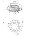
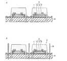
まず、本発明の第1実施形態に係る半導体発光装置について図面を参照して説明する。参照する図1は、第1実施形態に係る半導体発光装置の説明図であり、このうち、図1Aは、第1実施形態に係る半導体発光装置の斜視図、図1Bは、図1AのI−I線断面図、図1Cは、第1実施形態に係る半導体発光装置の蛍光体膜側から見た概略平面図である。[First Embodiment]
First, a semiconductor light emitting device according to a first embodiment of the present invention will be described with reference to the drawings. FIG. 1 to be referred to is an explanatory diagram of the semiconductor light emitting device according to the first embodiment. Of these, FIG. 1A is a perspective view of the semiconductor light emitting device according to the first embodiment, and FIG. FIG. 1C is a schematic plan view seen from the phosphor film side of the semiconductor light emitting device according to the first embodiment.
第1実施形態に係る半導体発光装置1は、図1A,Bに示すように、略正六角柱状に形成された電気絶縁基板10と、電気絶縁基板10上に設けられ、略円錐台状に形成された蛍光体膜11と、電気絶縁基板10上に設けられた半導体多層膜12と、半導体多層膜12に接触して設けられ、半導体多層膜12を結晶成長させる際に使用した単結晶基板13とを含む。そして、半導体多層膜12及び単結晶基板13は、蛍光体膜11で覆われている。また、単結晶基板13は、蛍光体膜11との接触面である主面13aが、凹凸加工されている。これにより、半導体発光装置1の光の取り出し効率が向上する。なお、主面13aに形成される凹凸において、凹部の深さは例えば0.1〜50μmであり、凸部のピッチは例えば0.5〜500μmである。 As shown in FIGS. 1A and 1B, the semiconductor
半導体多層膜12は、図1Bに示すように、電気絶縁基板10側から順に、例えばp型半導体からなる第1導電型層14と、発光層15と、例えばn型半導体からなる第2導電型層16とがこの順に積層されたダイオード構造からなる。そして、第2導電型層16は、発光層15から発せられた光の取り出し側に配置されている。また、図1Cに示すように、半導体多層膜12の最外縁となる第2導電型層16の外縁16aは、略正六角形状に形成されている。なお、蛍光体膜11は、発光層15から発せられた光を吸収して蛍光を発する蛍光体を含む。 As shown in FIG. 1B, the
また、半導体発光装置1は、上記構成に加え、図1Bに示すように、第1導電型層14の主面14aに形成された第1電極17と、第2導電型層16の突出部16bに形成された第2電極18と、電気絶縁基板10における半導体多層膜12側の主面10aに対する裏面10bに形成された第1端子19及び第2端子20と、第1電極17と第1端子19とを電気的に接続する第1導電部材21と、第2電極18と第2端子20とを電気的に接続する第2導電部材22とを含む。 In addition to the above configuration, the semiconductor
第1導電部材21は、第1端子19と接触し、かつ電気絶縁基板10に設けられたビアホール23内に形成されたビア導体24aと、ビア導体24aと接触し、かつ電気絶縁基板10の主面10a上に形成された導体パターン25aと、導体パターン25aと第1電極17とを電気的に接続するバンプ26aとを含む。また、第2導電部材22は、第2端子20と接触し、かつ電気絶縁基板10に設けられたビアホール23内に形成されたビア導体24bと、ビア導体24bと接触し、かつ電気絶縁基板10の主面10a上に形成された導体パターン25bと、導体パターン25bと第2電極18とを電気的に接続するバンプ26bとを含む。また、導体パターン25a,25bは、光を反射する材料を含み、図1Cに示すように、電気絶縁基板10の主面10aの略全面に形成されている。これにより、半導体発光装置1は、発光層15や蛍光体膜11から電気絶縁基板10側へと進む光を、導体パターン25a,25bにより光の取り出し側へと反射することができるため、光の取り出し効率が向上する。 The first
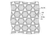
蛍光体膜11は、前述したように略円錐台状に形成されているため、電気絶縁基板10の主面10aに平行な方向に切断した断面の外縁が、略円形状に形成されている。これにより、半導体発光装置1は、蛍光体膜11から出射する光の異方性を低減させ、取り出される光の色ムラを抑えることができる上、点対称となるスポット光が得られるため、照明装置に適した光源を提供することができる。また、電気絶縁基板10は、前述したように略正六角柱状に形成されているため、図1Cに示すように、主面10aの外縁10cが、電気絶縁基板10上の蛍光体膜11が形成された領域10dを囲み、かつ略正六角形状に形成されている。これにより、半導体発光装置1は、電気絶縁基板10上に高密度に蛍光体膜11を形成することができるため、高光束化が可能となる上、後述する半導体発光装置1の製造工程において、電気絶縁基板10の外形加工を容易に行うことができる。 Since the
なお、電気絶縁基板10の主面10aの外縁10cにおいて、対角線の長さD1(図1C参照)は、例えば0.5〜5mmとすればよい。また、電気絶縁基板10上の蛍光体膜11が形成された領域10dの直径D2(図1C参照)は、例えば0.4〜4.5mmとすればよい。また、第2導電型層16の外縁16aにおいて、対角線の長さD3(図1C参照)は、例えば0.2〜4mmとすればよい。Incidentally, at the
このように構成された半導体発光装置1から光を取り出す際は、第1端子19と第2端子20との間に電圧を印加して、半導体発光装置1中に所定の電流を流す。これにより、発光層15から、例えば波長460nmの青色光が発せられる。そして、この青色光を蛍光体膜11中の蛍光体が吸収し、前記蛍光体から黄色光や赤色光が発せられる。そして、前記蛍光体から発せられた黄色光や赤色光と、発光層15から発せられ蛍光体膜11を通過した青色光とが混ざりあって、例えば白色光として照明光を取り出すことができる。 When light is extracted from the semiconductor
以上、本発明の第1実施形態に係る半導体発光装置について説明したが、本発明の半導体発光装置は、前記実施形態には限定されない。例えば、1つの基板上に複数の半導体多層膜を配置した半導体発光装置としてもよい。また、半導体多層膜の最外縁の形状も、前記実施形態には限定されず、例えば四角形状であってもよい。 The semiconductor light emitting device according to the first embodiment of the present invention has been described above, but the semiconductor light emitting device of the present invention is not limited to the above embodiment. For example, a semiconductor light emitting device in which a plurality of semiconductor multilayer films are arranged on one substrate may be used. Further, the shape of the outermost edge of the semiconductor multilayer film is not limited to the above embodiment, and may be, for example, a quadrangular shape.
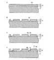
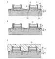
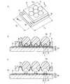
次に、本発明の第1実施形態に係る半導体発光装置1の製造方法について、適宜図面を参照して説明する。参照する図2〜図7は、第1実施形態に係る半導体発光装置1の製造方法の説明図であり、このうち図2〜図5は、第1実施形態に係る半導体発光装置1の製造方法の各工程を示す断面図で、図6は、半導体多層膜12を個別に分割する工程における上面図で、図7は、半導体発光装置1を個別に分割する工程における上面図である。なお、図1と同一の構成要素には同一の符号を付し、その説明は省略する。また、以下に説明する製造方法は、前述した本発明の半導体発光装置の第1の製造方法に係る一実施形態である。 Next, a method for manufacturing the semiconductor
まず、図2Aに示すように、MOCVD法等を用いて、単結晶基板13の主面13b上に、第2導電型層16、発光層15及び第1導電型層14を順次積層し、半導体多層膜12を形成する。単結晶基板13としては、例えば厚みが300μm程度のGaN基板等が使用できる。 First, as shown in FIG. 2A, the second
続いて、図2Bに示すように、第2導電型層16の突出部16b(図1B参照)を形成するために、第1導電型層14の一部及び発光層15の一部をドライエッチング等によりエッチングする。 Subsequently, as shown in FIG. 2B, in order to form the protruding
続いて、図2Cに示すように、第2導電型層16の一部をドライエッチング等によりエッチングし、半導体多層膜12を個別に分割するための分割溝16cを形成する。 Subsequently, as shown in FIG. 2C, a part of the second
続いて、図2Dに示すように、第1導電型層14の主面14a及び第2導電型層16の突出部16bにそれぞれ接触する第1電極17及び第2電極18を、電子ビーム蒸着法等によって形成する。 Subsequently, as shown in FIG. 2D, the
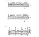
次に、図3Aに示すように、単結晶基板13の主面13aを、例えば単結晶基板13の厚みが200μm程度になるまで機械研磨等によって研磨する。 Next, as shown in FIG. 3A, the
続いて、図3Bに示すように、単結晶基板13の主面13aを、ドライエッチング等の手段を用いて凹凸加工する。これにより、形成される半導体発光装置1の光の取り出し効率が向上する。 Subsequently, as shown in FIG. 3B, the
続いて、図3Cに示すように、ダイシングブレード30によって、分割溝16cに沿って半導体多層膜12を個別に分割する。なお、分割溝16cは、図6に示す破線に沿って設けておくとよい。 Subsequently, as shown in FIG. 3C, the
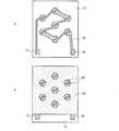
そして、別に、図4Aに示すように、電気絶縁基板10にドライエッチング等によってビアホール23を設けた後、このビアホール23内にビア導体24a,24bを形成する。ビア導体24a,24bは、例えばビアホール23内にPt等の金属をめっき等によって充填して形成すればよい。なお、電気絶縁基板10としては、例えば厚みが300μ程度の高純度Si基板等を使用することができる。 4A, a via
続いて、図4Bに示すように、電気絶縁基板10の主面10aに、ビア導体24a,24bと電気的に接続する導体パターン25a,25bを形成する。例えば、電気絶縁基板10の主面10a上に、Ti/Pt/Al膜等の金属膜を蒸着等によって形成した後、この金属膜をリフトオフ法等によって所望の形状にパターニングして導体パターン25a,25bを形成することができる。 Subsequently, as shown in FIG. 4B,
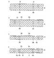
続いて、図4Cに示すように、電気絶縁基板10の裏面10bを、ビア導体24a,24bが露出するまで機械研磨等によって研磨する。例えば、電気絶縁基板10の厚みが200μm程度になるまで研磨すればよい。 Subsequently, as shown in FIG. 4C, the
続いて、図4Dに示すように、電気絶縁基板10の裏面10bに、ビア導体24a,24bを介して導体パターン25a,25bとそれぞれ電気的に接続する第1端子19及び第2端子20を形成する。例えば、電気絶縁基板10の裏面10b上においてビア導体24a,24bが露出している箇所に、電子ビーム蒸着法等によりTi/Au薄膜からなる下地膜を形成した後、この下地膜上にめっき等によってAu層を積層して第1及び第2端子19,20を形成することができる。 Subsequently, as shown in FIG. 4D, the
次に、図5Aに示すように、導体パターン25a,25b上に、それぞれバンプ26a,26bを形成する。 Next, as shown in FIG. 5A, bumps 26a and 26b are formed on the
続いて、図5Bに示すように、第1電極17と導体パターン25aとをバンプ26aを介して電気的に接続するとともに、第2電極18と導体パターン25bとをバンプ26bを介して電気的に接続して、電気絶縁基板10上に半導体多層膜12を支持する。 Subsequently, as shown in FIG. 5B, the
次に、図5Cに示すように、電気絶縁基板10上に、半導体多層膜12及び単結晶基板13を覆って蛍光体膜11を形成する。例えば、蛍光体とシリコーン樹脂等を含む樹脂組成物とからなるペーストと、略円錐台状の形状を模った孔部を含むスクリーン版とを用いて、スクリーン印刷により電気絶縁基板10上の半導体多層膜12及び単結晶基板13を覆う位置に蛍光体膜11を形成すればよい。なお、図5Cに示す状態において、電気絶縁基板10上に設けられた各々の半導体発光装置1(図5D参照)の電気的又は光学的な特性を検査することで、良品の半導体発光装置1のみを選別することができる。また、蛍光体膜11を機械研磨等により研磨して、取り出される光の色合わせをすることもできる。 Next, as shown in FIG. 5C, the
そして、図7に示す破線に沿って電気絶縁基板10上の蛍光体膜11が形成された領域10dを囲むようにして、図5Dに示すダイシングブレード30により電気絶縁基板10を略正六角柱状に切り抜く。これにより、電気絶縁基板10の主面10aの外縁10c(図7参照)が略正六角形状に形成され、半導体発光装置1が得られる。 Then, the electric insulating
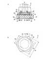
[第2実施形態]
次に、本発明の第2実施形態に係る半導体発光装置について図面を参照して説明する。参照する図8は、第2実施形態に係る半導体発光装置の説明図であり、このうち、図8Aは、第2実施形態に係る半導体発光装置の断面図、図8Bは、第2実施形態に係る半導体発光装置の蛍光体膜側から見た概略平面図である。なお、図8Bでは、基板、蛍光体膜及び半導体多層膜のみを図示している。また、図1と同一の構成要素には同一の符号を付し、その説明は省略する。[Second Embodiment]
Next, a semiconductor light emitting device according to a second embodiment of the invention will be described with reference to the drawings. FIG. 8 to be referred to is an explanatory diagram of the semiconductor light emitting device according to the second embodiment. Of these, FIG. 8A is a cross-sectional view of the semiconductor light emitting device according to the second embodiment, and FIG. 8B is the second embodiment. It is the schematic plan view seen from the fluorescent substance film side of the semiconductor light-emitting device which concerns. FIG. 8B shows only the substrate, the phosphor film, and the semiconductor multilayer film. Moreover, the same code | symbol is attached | subjected to the component same as FIG. 1, and the description is abbreviate | omitted.
第2実施形態に係る半導体発光装置2は、図8A,Bに示すように、略正六角柱状に形成された電気絶縁基板10と、電気絶縁基板10上に設けられ、略円錐台状に形成された蛍光体膜11と、電気絶縁基板10上に設けられた半導体多層膜12とを含む。そして、半導体多層膜12は、蛍光体膜11で覆われている。電気絶縁基板10としては、電気絶縁性を高めるため、高純度Si基板40と酸化シリコン絶縁膜41とが積層されたものを使用している。 As shown in FIGS. 8A and 8B, the semiconductor light emitting device 2 according to the second embodiment is formed in a substantially regular hexagonal column shape, and is provided on the
半導体多層膜12は、図8Aに示すように、電気絶縁基板10側から順に、例えばp型半導体からなる第1導電型層14と、発光層15と、例えばn型半導体からなる第2導電型層16とがこの順に積層されたダイオード構造からなる。そして、第2導電型層16は、発光層15から発せられた光の取り出し側に配置されている。また、第2導電型層16は、蛍光体膜11との接触面である主面16dが、凹凸加工されている。これにより、半導体発光装置2の光の取り出し効率が向上する。また、図8Bに示すように、半導体多層膜12の最外縁12aは、略円形状に形成されている。 As shown in FIG. 8A, the
また、半導体発光装置2は、上記構成に加え、図8Aに示すように、第1導電型層14の主面14aに形成された第1電極17と、第2導電型層16の主面16dの一部に接触して形成された第2電極18と、高純度Si基板40の主面40aに形成された第1端子19及び第2端子20と、第1電極17と第1端子19とを電気的に接続する第1導電部材21と、第2電極18と第2端子20とを電気的に接続する第2導電部材22と、第1電極17と第2電極18との間の絶縁を保つ窒化シリコン絶縁膜42とを含む。 In addition to the above configuration, the semiconductor light emitting device 2 includes a
第1導電部材21は、第1端子19と接触し、かつ電気絶縁基板10に設けられたビアホール23内に形成されたビア導体24aと、ビア導体24aと接触し、かつ酸化シリコン絶縁膜41の主面41a上に形成された導体パターン25aと、導体パターン25aと第1電極17とを電気的に接続する金属層43とを含む。また、第2導電部材22は、第2電極18及び第2端子20の双方と接触し、かつ電気絶縁基板10に設けられたビアホール23内に形成されたビア導体24bからなる。 The first
蛍光体膜11は、前述したように略円錐台状に形成されているため、電気絶縁基板10における半導体多層膜12側の主面、即ち酸化シリコン絶縁膜41の主面41aに平行な方向に切断した断面の外縁が、略円形状に形成されている。これにより、半導体発光装置2は、蛍光体膜11から出射する光の異方性を低減させ、取り出される光の色ムラを抑えることができる上、点対称となるスポット光が得られるため、照明装置に適した光源を提供することができる。また、電気絶縁基板10は、前述したように略正六角柱状に形成されているため、図8Bに示すように、酸化シリコン絶縁膜41の主面41aの外縁41bが、酸化シリコン絶縁膜41上の蛍光体膜11が形成された領域41cを囲み、かつ略正六角形状に形成されている。これにより、半導体発光装置2は、酸化シリコン絶縁膜41上に高密度に蛍光体膜11を形成することができるため、高光束化が可能となる上、後述する半導体発光装置2の製造工程において、電気絶縁基板10の外形加工を容易に行うことができる。 Since the
また、半導体発光装置2は、図8Aに示すように、第1電極17が第1導電型層14の主面14aに接触して形成され、蛍光体膜11が第2導電型層16の主面16dに接触して形成されている。これにより、半導体多層膜12の両主面上に、半導体多層膜12を結晶成長させる際に使用した単結晶基板が存在しないため、半導体発光装置2の全体を薄く構成することができる。更に、発光層15から発せられた光が単結晶基板を通過せずに放出されるため、光の取り出し効率が向上する。 Further, as shown in FIG. 8A, in the semiconductor light emitting device 2, the
なお、酸化シリコン絶縁膜41の主面41aの外縁41bにおいて、対角線の長さD4(図8B参照)は、例えば0.5〜5mmとすればよい。また、酸化シリコン絶縁膜41上の蛍光体膜11が形成された領域41cの直径D5(図8B参照)は、例えば0.4〜4.5mmとすればよい。また半導体多層膜12の最外縁12aの直径D6(図8B参照)は、例えば0.2〜4mmとすればよい。The diagonal length D4 (see FIG. 8B) at the
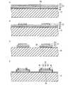
次に、本発明の第2実施形態に係る半導体発光装置2の製造方法について、適宜図面を参照して説明する。参照する図9〜図14は、第2実施形態に係る半導体発光装置2の製造方法の各工程を示す断面図である。なお、図8と同一の構成要素には同一の符号を付し、その説明は省略する。また、以下に説明する製造方法は、前述した本発明の半導体発光装置の第2の製造方法に係る一実施形態である。 Next, a method for manufacturing the semiconductor light emitting device 2 according to the second embodiment of the present invention will be described with reference to the drawings as appropriate. 9 to 14 to be referred to are cross-sectional views showing respective steps of the method for manufacturing the semiconductor light emitting device 2 according to the second embodiment. In addition, the same code | symbol is attached | subjected to the component same as FIG. 8, and the description is abbreviate | omitted. The manufacturing method described below is an embodiment according to the second manufacturing method of the semiconductor light emitting device of the present invention described above.
まず、図9Aに示すように、MOCVD法等を用いて、単結晶基板50の主面50a上に、第2導電型層16、発光層15及び第1導電型層14を順次積層し、半導体多層膜12を形成する。単結晶基板50としては、例えば300μm程度のサファイア基板等が使用できる。 First, as shown in FIG. 9A, the second
続いて、図9Bに示すように、略円柱状の半導体多層膜12が残るように半導体多層膜12の一部をドライエッチング等によりエッチングする。 Subsequently, as shown in FIG. 9B, a part of the
続いて、図9Cに示すように、第1導電型層14の主面14aに接触する第1電極17を、電子ビーム蒸着法等によって形成する。 Subsequently, as shown in FIG. 9C, the
そして、別に、図10Aに示すように、高純度Si基板40と酸化シリコン絶縁膜41とが積層された電気絶縁基板10を用意する。そして、ドライエッチング等により、酸化シリコン絶縁膜41と高純度Si基板40の一部とを貫通するビアホール23を設けた後、このビアホール23内にビア導体24a,24bを形成する。ビア導体24a,24bは、例えばビアホール23内にPt等の金属をめっき等によって充填して形成すればよい。なお、電気絶縁基板10としては、例えば厚みが300μm程度の高純度Si基板40と、厚みが0.5μm程度の酸化シリコン絶縁膜41とが積層されたものを使用することができる。 Separately, as shown in FIG. 10A, an electrically insulating
続いて、図10Bに示すように、酸化シリコン絶縁膜41の主面41aに、ビア導体24aと電気的に接続する導体パターン25aを形成する。例えば、酸化シリコン絶縁膜41の主面41a上に、Ti/Pt/Au膜等の金属膜を蒸着等によって形成した後、この金属膜をリフトオフ法等によって所望の形状にパターニングして導体パターン25aを形成することができる。次に、導体パターン25a上に、例えばめっき等によりAu/Sn層等の金属層43を形成する。 Subsequently, as shown in FIG. 10B, a
続いて、図10Cに示すように、第1電極17と金属層43とを、例えば金属層43が溶融する温度(例えば300℃程度)で加熱して接合させることにより、単結晶基板50と電気絶縁基板10との間に半導体多層膜12を挟持した積層体51を形成する。 Subsequently, as shown in FIG. 10C, the
そして、単結晶基板50を半導体多層膜12から分離する。例えば、図11Aに示すように、単結晶基板50側からレーザ光LBを照射することにより、単結晶基板50と半導体多層膜12との界面における結合力を低下させた後、図11Bに示すように、単結晶基板50を半導体多層膜12(即ち、第2導電型層16)から分離すればよい。なお、単結晶基板50を分離した後、第2導電型層16上に残留する金属(例えばGa等)を塩酸等によって除去することが好ましい。 Then, the
続いて、図11Cに示すように、酸化シリコン絶縁膜41上及び半導体多層膜12の周囲の所望の箇所に、窒化シリコン絶縁膜42を形成する。例えば、半導体多層膜12を覆って酸化シリコン絶縁膜41上の全面に、高周波スパッタ法等により厚み0.3〜1μm程度の窒化シリコン絶縁膜42を形成した後、絶縁を保つ必要がある箇所のみが残るように、窒化シリコン絶縁膜42をドライエッチング等によりエッチングすればよい。 Subsequently, as illustrated in FIG. 11C, a silicon
次に、図12Aに示すように、第2導電型層16とビア導体24bとを電気的に接続する第2電極18を形成する。例えば、第2導電型層16とビア導体24bとの接続箇所に、Ti/Pt/Al膜等の金属膜を蒸着等によって形成すればよい。 Next, as shown in FIG. 12A, the
続いて、図12Bに示すように、第2導電型層16の主面16dを、ドライエッチング等の手段を用いて凹凸加工する。これにより、形成される半導体発光装置2の光の取り出し効率が向上する。 Subsequently, as shown in FIG. 12B, the
続いて、図12Cに示すように、半導体多層膜12を覆って電気絶縁基板10上の全面に、剥離可能な高分子フィルム52を貼り合わせる。例えば、ポリエステル等からなり、加熱すると発泡して接着力がなくなる接着層(不図示)を介して、電気絶縁基板10上に高分子フィルム52を貼り合わせればよい。この高分子フィルム52は、製造工程におけるハンドリングを容易にするための支持部材として用いられる。なお、高分子フィルム52としては、例えば、ポリエステル系フィルムやポリイミド系フィルム等からなり、厚みが0.5〜1mm程度のフィルムが使用できる。 Subsequently, as shown in FIG. 12C, a
次に、図13Aに示すように、高純度Si基板40の主面40aを、ビア導体24a,24bが露出するまで機械研磨等によって研磨する。例えば、電気絶縁基板10の厚みが200μm程度になるまで研磨すればよい。 Next, as shown in FIG. 13A, the
続いて、図13Bに示すように、高純度Si基板40の主面40aに、ビア導体24aを介して導体パターン25aと電気的に接続する第1端子19と、ビア導体24bを介して第2電極18と電気的に接続する第2端子20とを形成する。例えば、高純度Si基板40の主面40a上においてビア導体24a,24bが露出している箇所に、電子ビーム蒸着法等によりTi/Au薄膜からなる下地膜を形成した後、この下地膜上にめっき等によってAu層を積層して第1及び第2端子19,20を形成することができる。 Subsequently, as shown in FIG. 13B, the
続いて、高分子フィルム52を剥離し、図13Cに示すように、第1及び第2端子19,20を覆って高純度Si基板40の主面40aの全面に、剥離可能な高分子フィルム53を貼り合わせる。高分子フィルム53の材料や貼り合わせる方法は、前述した高分子フィルム52の場合と同様である。 Subsequently, the
次に、図14Aに示すように、電気絶縁基板10上に、第2導電型層16の主面16dに接触し、かつ半導体多層膜12を覆って蛍光体膜11を形成する。蛍光体膜11の形成方法は、前述した半導体発光装置1の製造方法の場合(図5C参照)と同様である。なお、図14Aに示す状態において、電気絶縁基板10上に設けられた各々の半導体発光装置2(図14B参照)の電気的又は光学的な特性を検査することで、良品の半導体発光装置2のみを選別することができる。また、蛍光体膜11を機械研磨等により研磨して、取り出される光の色合わせをすることもできる。 Next, as shown in FIG. 14A, the
そして、前述した半導体発光装置1の製造方法の場合(図7参照)と同様に、図14Bに示すダイシングブレード30によって、電気絶縁基板10及び高分子フィルム53を略正六角柱状に切り抜く。これにより、酸化シリコン絶縁膜41の主面41aの外縁41b(図8B参照)が、略正六角形状に形成される。そして、高分子フィルム53を剥離し(図示せず)、半導体発光装置2が得られる。 Then, as in the case of the method for manufacturing the semiconductor
[第3実施形態]
次に、本発明の第3実施形態に係る半導体発光装置について図面を参照して説明する。参照する図15は、第3実施形態に係る半導体発光装置の説明図であり、このうち、図15Aは、第3実施形態に係る半導体発光装置の断面図、図15Bは、第3実施形態に係る半導体発光装置の蛍光体膜側から見た概略平面図である。なお、図15Bでは、基板、蛍光体膜及び半導体多層膜のみを図示している。また、図1及び図8と同一の構成要素には同一の符号を付し、その説明は省略する。[Third Embodiment]
Next, a semiconductor light-emitting device according to a third embodiment of the present invention will be described with reference to the drawings. FIG. 15 to be referred to is an explanatory diagram of the semiconductor light emitting device according to the third embodiment. Of these, FIG. 15A is a cross-sectional view of the semiconductor light emitting device according to the third embodiment, and FIG. It is the schematic plan view seen from the fluorescent substance film side of the semiconductor light-emitting device which concerns. FIG. 15B shows only the substrate, the phosphor film, and the semiconductor multilayer film. Moreover, the same code | symbol is attached | subjected to the component same as FIG.1 and FIG.8, and the description is abbreviate | omitted.
第3実施形態に係る半導体発光装置3は、図15A,Bに示すように、略正六角柱状に形成された電気絶縁基板10と、電気絶縁基板10上に設けられ、略円錐台状に形成された蛍光体膜11と、電気絶縁基板10上に設けられた半導体多層膜12とを含む。そして、半導体多層膜12は、蛍光体膜11で覆われている。 As shown in FIGS. 15A and 15B, the semiconductor
半導体多層膜12は、図15Aに示すように、電気絶縁基板10側から順に、例えばn型半導体からなる第1導電型層14と、発光層15と、例えばp型半導体からなる第2導電型層16とがこの順に積層されたダイオード構造からなる。そして、第2導電型層16は、発光層15から発せられた光の取り出し側に配置されている。また、図15Bに示すように、半導体多層膜12の最外縁12aは、略円形状に形成されている。 As shown in FIG. 15A, the
また、半導体発光装置3は、上記構成に加え、図15Aに示すように、第1導電型層14に接触する第1電極17と、第2導電型層16に接触する第2電極18と、電気絶縁基板10における半導体多層膜12側の主面10aに対する裏面10bに形成された第1端子19及び第2端子20と、第1電極17と第1端子19とを電気的に接続する第1導電部材21と、第2電極18と第2端子20とを電気的に接続する第2導電部材22と、第1電極17と第2電極18との間の絶縁を保つ窒化シリコン絶縁膜42とを含む。 In addition to the above configuration, the semiconductor
第1導電部材21は、第1電極17及び第1端子19の双方と接触し、かつ電気絶縁基板10に設けられたビアホール23内に形成されたビア導体24aからなる。また、第2導電部材22は、第2電極18及び第2端子20の双方と接触し、かつ電気絶縁基板10に設けられたビアホール23内に形成されたビア導体24bからなる。 The first
蛍光体膜11は、前述したように略円錐台状に形成されているため、電気絶縁基板10の主面10aに平行な方向に切断した断面の外縁が、略円形状に形成されている。これにより、半導体発光装置3は、蛍光体膜11から出射する光の異方性を低減させ、取り出される光の色ムラを抑えることができる上、点対称となるスポット光が得られるため、照明装置に適した光源を提供することができる。また、電気絶縁基板10は、前述したように略正六角柱状に形成されているため、図15Bに示すように、電気絶縁基板10の主面10aの外縁10cが、電気絶縁基板10上の蛍光体膜11が形成された領域10dを囲み、かつ略正六角形状に形成されている。これにより、半導体発光装置3は、電気絶縁基板10上に高密度に蛍光体膜11を形成することができるため、高光束化が可能となる上、後述する半導体発光装置3の製造工程において、電気絶縁基板10の外形加工を容易に行うことができる。 Since the
また半導体発光装置3は、図15Aに示すように、第1導電型層14と電気絶縁基板10との間に介在するミラー層60を含む。ミラー層60としては、例えば、AlGaN層とGaN層とを交互に複数層重ねた積層体であって、厚みが1〜3μm程度のものが使用できる。これにより、半導体発光装置3は、発光層15から電気絶縁基板10側へと進む光のうち照明光として必要な光のみを、ミラー層60によって選択的に光の取り出し側へと反射することができる。 Further, as shown in FIG. 15A, the semiconductor
なお、電気絶縁基板10の主面10aの外縁10cにおいて、対角線の長さD7(図15B参照)は、例えば0.5〜5mmとすればよい。また、電気絶縁基板10上の蛍光体膜11が形成された領域10dの直径D8(図15B参照)は、例えば0.4〜4.5mmとすればよい。また半導体多層膜12の最外縁12aの直径D9(図15B参照)は、例えば0.2〜4mmとすればよい。In addition, at the
次に、本発明の第3実施形態に係る半導体発光装置3の製造方法について、適宜図面を参照して説明する。参照する図16〜図18は、第3実施形態に係る半導体発光装置3の製造方法の各工程を示す断面図である。なお、図15と同一の構成要素には同一の符号を付し、その説明は省略する。 Next, a method for manufacturing the semiconductor
まず、図16Aに示すように、MOCVD法等を用いて、電気絶縁基板10の主面10a上にミラー層60を積層した後、ミラー層60上に、MOCVD法等を用いて、第1導電型層14、発光層15及び第2導電型層16を順次積層し、半導体多層膜12を形成する。電気絶縁基板10としては、例えば300μm程度の高純度SiC基板等が使用できる。 First, as shown in FIG. 16A, after the
続いて、図16Bに示すように、第2導電型層16の一部及び発光層15の一部をドライエッチング等によりエッチングする。次に、図16Cに示すように、第1導電型層14の一部及びミラー層60の一部をドライエッチング等によりエッチングする。この際、第1導電型層14及び発光層15により段差が形成され、かつ半導体多層膜12の最外縁12a(図15B参照)が略円形状に残るようにエッチングする。 Subsequently, as shown in FIG. 16B, a part of the second
続いて、図16Dに示すように、電気絶縁基板10上及び半導体多層膜12の周囲の所望の箇所に、窒化シリコン絶縁膜42を形成する。窒化シリコン絶縁膜42の形成方法は、前述した半導体発光装置2の製造方法の場合(図11C参照)と同様である。 Subsequently, as illustrated in FIG. 16D, a silicon
次に、図17Aに示すように、ドライエッチング等により、窒化シリコン絶縁膜42と電気絶縁基板10の一部とを貫通するビアホール23を設けた後、このビアホール23内にビア導体24a,24bを形成する。ビア導体24a,24bは、例えばビアホール23内にPt等の金属をめっき等によって充填して形成すればよい。 Next, as shown in FIG. 17A, a via
続いて、図17Bに示すように、第1導電型層14とビア導体24aとを電気的に接続する第1電極17を形成するとともに、第2導電型層16とビア導体24bとを電気的に接続する第2電極18を形成する。例えば、第1導電型層14とビア導体24aとの接続箇所、及び第2導電型層16とビア導体24bとの接続箇所に、Ti/Pt/Al膜等の金属膜を蒸着等によって形成すればよい。 Subsequently, as shown in FIG. 17B, the
続いて、図17Cに示すように、電気絶縁基板10の裏面10bを、ビア導体24a,24bが露出するまで機械研磨等によって研磨する。例えば、電気絶縁基板10の厚みが200μm程度になるまで研磨すればよい。 Subsequently, as shown in FIG. 17C, the
続いて、図17Dに示すように、電気絶縁基板10の裏面10bに、ビア導体24aを介して第1電極17と電気的に接続する第1端子19と、ビア導体24bを介して第2電極18と電気的に接続する第2端子20とを形成する。第1及び第2端子19,20の形成方法は、前述した半導体発光装置2の製造方法の場合(図13B参照)と同様である。 Subsequently, as shown in FIG. 17D, a
次に、図18Aに示すように、電気絶縁基板10上に、半導体多層膜12を覆って蛍光体膜11を形成する。蛍光体膜11の形成方法は、前述した半導体発光装置1の製造方法の場合(図5C参照)と同様である。なお、図18Aに示す状態において、電気絶縁基板10上に設けられた各々の半導体発光装置3(図18B参照)の電気的又は光学的な特性を検査することで、良品の半導体発光装置3のみを選別することができる。また、蛍光体膜11を機械研磨等により研磨して、取り出される光の色合わせをすることもできる。 Next, as shown in FIG. 18A, the
そして、前述した半導体発光装置1の製造方法の場合(図7参照)と同様に、図18Bに示すダイシングブレード30によって、電気絶縁基板10を略正六角柱状に切り抜く。これにより、電気絶縁基板10の主面10aの外縁10c(図15B参照)が、略正六角形状に形成され、半導体発光装置3が得られる。 Then, as in the case of the method for manufacturing the semiconductor
[第4実施形態]
次に、本発明の第4実施形態に係る照明モジュールについて適宜図面を参照して説明する。参照する図19は、第4実施形態に係る照明モジュールの説明図であり、このうち図19Aは、第4実施形態に係る照明モジュールの斜視図、図19Bは、図19AのII−II線断面図、図19Cは、図19Bに図示した第4実施形態に係る照明モジュールの分解図である。なお、第4実施形態に係る照明モジュールは、前述した第1実施形態に係る半導体発光装置1を含む照明モジュールである。また、図1と同一の構成要素には同一の符号を付し、その説明は省略する。[Fourth Embodiment]
Next, an illumination module according to a fourth embodiment of the present invention will be described with reference to the drawings as appropriate. FIG. 19 to be referred to is an explanatory diagram of the illumination module according to the fourth embodiment, in which FIG. 19A is a perspective view of the illumination module according to the fourth embodiment, and FIG. 19B is a cross-sectional view taken along the line II-II in FIG. 19C is an exploded view of the illumination module according to the fourth embodiment illustrated in FIG. 19B. In addition, the illumination module which concerns on 4th Embodiment is an illumination module containing the semiconductor light-emitting
第4実施形態に係る照明モジュール4は、図19A,Bに示すように、基板70と、基板70上に実装された7個の半導体発光装置1と、半導体発光装置1を覆って基板70上に貼り合わされたレンズ71とを含む。 19A and 19B, the
基板70は、図19Bに示すように、アルミニウム板72と、アルミニウム板72上に積層された第1電気絶縁層73と、第1電気絶縁層73上に積層された第2電気絶縁層74と、第1電気絶縁層73と第2電気絶縁層74との間に形成された配線パターン75とを含む。また、配線パターン75の端部は、図19Aに示す第1給電端子76及び第2給電端子77となっている。そして、半導体発光装置1は、配線パターン75上にフリップチップ実装されている。なお、本実施形態では、第1及び第2電気絶縁層73,74の材料として、エポキシ樹脂等の熱硬化性樹脂とアルミナ等の無機フィラとを含むコンポジット材を使用した。 As shown in FIG. 19B, the
レンズ71は、図19Cに示すように、各々の半導体発光装置1に対応する凸部71aと、半導体発光装置1が発する光を反射するアルミニウム膜71bとを含む。そして、基板70上に、エポキシ樹脂等の接着剤78(図19B参照)によって貼り合わされている。 As shown in FIG. 19C, the
以上のように構成された照明モジュール4は、本発明の一実施形態である半導体発光装置1を含むため、取り出される光の色ムラを抑えることができる上、高光束化が可能となる。 Since the
なお、本実施形態で使用した基板70は、アルミニウム板72、第1電気絶縁層73及び第2電気絶縁層74の厚みが、それぞれ1mm、0.5mm及び0.5mmであり、図19Aに示す縦方向の長さ(L1)及び横方向の長さ(L2)が、それぞれ28mm及び24mmである。また、本実施形態で使用したレンズ71としては、凸部71aの最大厚みが5mmのものを用いた。In the
また、本実施形態で使用した半導体発光装置1(図1参照)の各構成要素の材料、サイズ等は、電気絶縁基板10:高純度Si基板(厚み:0.2mm、D1(図1C参照):2mm)、導体パターン25a,25b(図1参照)を基準としたときの蛍光体膜11の高さ:0.4mm、第1導電型層14:p−GaN層、発光層15:InGaN/GaN量子井戸発光層、第2導電型層16:n−GaN層、半導体多層膜12の厚み:3μm、単結晶基板13:GaN基板(厚み:0.2mm)、電気絶縁基板10上の蛍光体膜11が形成された領域10dの直径D2(図1C参照):1.8mm、第2導電型層16の外縁16aにおける対角線の長さD3(図1C参照):1mmとした。Further, the material, size, and the like of each component of the semiconductor light emitting device 1 (see FIG. 1) used in the present embodiment are as follows: electrical insulating substrate 10: high-purity Si substrate (thickness: 0.2 mm, D1 (see FIG. 1C) ): 2 mm), the height of the
次に、照明モジュール4の製造方法について適宜図面を参照して説明する。参照する図20A,B及び図21A,Bは、照明モジュール4の製造方法の各工程を説明するための平面図である。なお、図19と同一の構成要素には同一の符号を付し、その説明は省略する。 Next, the manufacturing method of the
まず、アルミニウム板72(図19B参照)上に熱圧着により第1電気絶縁層73を形成し、第1電気絶縁層73の主面に転写によって図20Aに示す配線パターン75を形成する。 First, the first
続いて、図20Bに示すように、第1電気絶縁層73上に、半導体発光装置1の実装箇所80に対応する孔が形成された第2電気絶縁層74を積層し、熱圧着する。 Subsequently, as shown in FIG. 20B, a second electrical insulating
次に、図21Aに示すように、配線パターン75の実装箇所80(図20B参照)に、半導体発光装置1を実装する。そして、図21Bに示すように、第2電気絶縁層74上にレンズ71を貼り合わせて、照明モジュール4が得られる。 Next, as shown in FIG. 21A, the semiconductor
次に、照明モジュール4の特性について説明する。照明モジュール4に対して、駆動電圧24.5Vにて350mAの電流を流すと、取り出される照明光の全光束は400lmとなり、その発光スペクトルは図22に示すとおりとなった。また、この際の照明光の発光色は、図23に示すx−y色度座標中の黒体軌跡90上の点A(x:0.4369、y:0.4041)に相当し、その色温度Tcは3000Kで、その平均演色評価数Raは95であった。なお、図23に示すx−y色度座標中の曲線91は、380〜780nmの単色光の軌跡を示す。 Next, the characteristics of the
[第5実施形態]
次に、本発明の第5実施形態に係る照明装置について適宜図面を参照して説明する。参照する図24は、第5実施形態に係る照明装置の斜視図である。なお、第5実施形態に係る照明装置は、前述した第4実施形態に係る照明モジュール4を含む照明装置である。[Fifth Embodiment]
Next, a lighting device according to a fifth embodiment of the present invention will be described with reference to the drawings as appropriate. FIG. 24 to be referred to is a perspective view of the illumination device according to the fifth embodiment. In addition, the illuminating device which concerns on 5th Embodiment is an illuminating device containing the
図24に示すように、照明装置5は、一般の白熱電球用ソケットにねじ込むタイプの口金100と、口金100の端部に固定されたケース101と、ケース101に取り付けられた照明モジュール4と、照明モジュール4を駆動させる駆動回路(図示せず)とを含む。 As shown in FIG. 24, the
ケース101は、口金100と対向する平面101aに、照明モジュール4を取り付けるための収納部101bを有している。そして、照明モジュール4は、ケース101の収納部101bに収納されている。また、収納部101b内には、前記駆動回路と接続する給電部(図示せず)が設けられており、この給電部は、照明モジュール4に対して、所定の駆動電流を流すことができる。 The
以上のように構成された照明装置5は、本発明の一実施形態である照明モジュール4を光源として使用するため、取り出される光の色ムラを抑えることができる上、高光束化が可能となる。 Since the
1,2,3 半導体発光装置
4 照明モジュール
5 照明装置
10 電気絶縁基板(基板)
10a,14a,16d,40a,41a,50a 主面
10b 裏面
10c,16a,41b 外縁
10d,41c 領域
11 蛍光体膜
12 半導体多層膜
12a 最外縁
13,50 単結晶基板
14 第1導電型層
15 発光層
16 第2導電型層
17 第1電極
18 第2電極
19 第1端子
20 第2端子
21 第1導電部材
22 第2導電部材
23 ビアホール
24a,24b ビア導体
25a,25b 導体パターン
26a,26b バンプ
30 ダイシングブレード
40 高純度Si基板
41 酸化シリコン絶縁膜
43 金属層
51 積層体
60 ミラー層
70 基板
71 レンズ
100 口金
101 ケース
LB レーザ光
1, 2, 3 Semiconductor
10a, 14a, 16d, 40a, 41a,
Claims (12)
Translated fromJapanese前記第1導電型層に接触して形成された第1電極と、
前記第2導電型層に接触して形成された第2電極と、
前記半導体多層膜の前記第1導電型層側に配置され、前記半導体多層膜を支持する基板と、
前記基板における前記半導体多層膜側の主面に対する裏面に形成された第1及び第2端子と、
前記第1電極と前記第1端子とを電気的に接続する第1導電部材と、
前記第2電極と前記第2端子とを電気的に接続する第2導電部材と、
前記半導体多層膜を覆って前記基板上に形成され、前記発光層から発せられた光を吸収して蛍光を発する蛍光体を含む蛍光体膜とを有する半導体発光装置であって、
前記蛍光体膜は、前記基板における前記半導体多層膜側の主面に平行な方向に切断した断面の外縁が、略円形状又は5つ以上の辺を有する略正多角形状に形成され、
前記基板における前記半導体多層膜側の主面の外縁は、前記基板上の前記蛍光体膜が形成された領域を囲み、かつ略円形状又は5つ以上の辺を有する略正多角形状に形成されていることを特徴とする半導体発光装置。A semiconductor multilayer film in which a first conductivity type layer, a light emitting layer, and a second conductivity type layer disposed on a light extraction side of the light emitted from the light emitting layer are laminated in this order;
A first electrode formed in contact with the first conductivity type layer;
A second electrode formed in contact with the second conductivity type layer;
A substrate disposed on the first conductivity type layer side of the semiconductor multilayer film and supporting the semiconductor multilayer film;
First and second terminals formed on the back surface of the substrate with respect to the main surface on the semiconductor multilayer film side;
A first conductive member that electrically connects the first electrode and the first terminal;
A second conductive member that electrically connects the second electrode and the second terminal;
A semiconductor light-emitting device comprising a phosphor film that covers the semiconductor multilayer film and is formed on the substrate and includes a phosphor that emits fluorescence by absorbing light emitted from the light-emitting layer,
The phosphor film has an outer edge of a cross section cut in a direction parallel to the main surface on the semiconductor multilayer film side of the substrate, and is formed in a substantially circular shape or a substantially regular polygonal shape having five or more sides,
The outer edge of the main surface of the substrate on the semiconductor multilayer film side is formed in a substantially circular shape or a substantially regular polygonal shape having five or more sides surrounding the region on the substrate where the phosphor film is formed. A semiconductor light-emitting device.
前記蛍光体膜は、前記第2導電型層の主面に接触して形成されている請求項1に記載の半導体発光装置。The first electrode is formed in contact with the main surface of the first conductivity type layer,
The semiconductor light emitting device according to claim 1, wherein the phosphor film is formed in contact with a main surface of the second conductivity type layer.
前記導体パターンは、前記基板における前記半導体多層膜側の主面の略全面に形成されている請求項1に記載の半導体発光装置。The first and second conductive members have a conductor pattern including a material that reflects light,
The semiconductor light emitting device according to claim 1, wherein the conductor pattern is formed on substantially the entire main surface of the substrate on the semiconductor multilayer film side.
前記第1及び第2導電型層にそれぞれ接触する第1及び第2電極を形成し、
別に、基板にビアホールを設けた後、前記ビアホール内にビア導体を形成し、
前記基板の一主面に、前記ビア導体と電気的に接続する導体パターンを形成し、
前記基板の前記一主面に対する裏面に、前記ビア導体を介して前記導体パターンとそれぞれ電気的に接続する第1及び第2端子を形成し、
前記第1電極と前記第1端子とを前記導体パターン及び前記ビア導体を介して電気的に接続するとともに、前記第2電極と前記第2端子とを前記導体パターン及び前記ビア導体を介して電気的に接続して、前記基板上に前記半導体多層膜を支持し、
前記基板上に、前記発光層から発せられた光を吸収して蛍光を発する蛍光体を含む蛍光体膜を、前記半導体多層膜を覆い、かつ前記基板における前記半導体多層膜側の主面に平行な方向に切断した断面の外縁が略円形状又は5つ以上の辺を有する略正多角形状となるように形成し、
前記基板上の前記蛍光体膜が形成された領域を囲み、かつ前記領域を含む前記基板の主面の外縁が略円形状又は5つ以上の辺を有する略正多角形状となるように前記基板を切り抜く半導体発光装置の製造方法。On one main surface of the single crystal substrate, a first conductivity type layer, a light emitting layer, and a second conductivity type layer disposed on a light extraction side of light emitted from the light emitting layer from a distance from the single crystal substrate. A semiconductor multilayer film including this order is formed by crystal growth,
Forming first and second electrodes in contact with the first and second conductivity type layers, respectively;
Separately, after providing a via hole in the substrate, forming a via conductor in the via hole,
Forming a conductor pattern electrically connected to the via conductor on one main surface of the substrate;
Forming first and second terminals respectively electrically connected to the conductor pattern through the via conductors on the back surface of the substrate with respect to the one main surface;
The first electrode and the first terminal are electrically connected via the conductor pattern and the via conductor, and the second electrode and the second terminal are electrically connected via the conductor pattern and the via conductor. Connected to support the semiconductor multilayer film on the substrate,
A phosphor film containing a phosphor that emits fluorescence by absorbing light emitted from the light emitting layer on the substrate covers the semiconductor multilayer film and is parallel to the main surface of the substrate on the semiconductor multilayer film side. Formed so that the outer edge of the cross section cut in any direction becomes a substantially circular shape or a substantially regular polygonal shape having five or more sides,
The substrate surrounding the region where the phosphor film is formed on the substrate and having an outer edge of a main surface of the substrate including the region in a substantially circular shape or a substantially regular polygonal shape having five or more sides. Of manufacturing semiconductor light emitting device.
前記第1導電型層の主面に接触する第1電極を形成し、
別に、基板にビアホールを設けた後、前記ビアホール内にビア導体を形成し、
前記基板の一主面に、前記ビア導体と電気的に接続する導体パターンを形成し、
前記導体パターン上に、金属層を形成し、
前記第1電極と前記金属層とを接合させることにより、前記単結晶基板と前記基板との間に前記半導体多層膜を挟持した積層体を形成し、
前記単結晶基板を前記半導体多層膜から分離し、
前記第2導電型層と前記ビア導体とを電気的に接続する第2電極を形成し、
前記基板の前記一主面に対する裏面に、前記ビア導体を介して前記導体パターンと電気的に接続する第1端子と、前記ビア導体を介して前記第2電極と電気的に接続する第2端子とを形成し、
前記基板上に、前記発光層から発せられた光を吸収して蛍光を発する蛍光体を含む蛍光体膜を、前記第2導電型層の主面に接触して前記半導体多層膜を覆い、かつ前記基板における前記半導体多層膜側の主面に平行な方向に切断した断面の外縁が略円形状又は5つ以上の辺を有する略正多角形状となるように形成し、
前記基板上の前記蛍光体膜が形成された領域を囲み、かつ前記領域を含む前記基板の主面の外縁が略円形状又は5つ以上の辺を有する略正多角形状となるように前記基板を切り抜く半導体発光装置の製造方法。On one main surface of the single crystal substrate, a first conductivity type layer, a light emitting layer, and a second conductivity type layer disposed on a light extraction side of light emitted from the light emitting layer from a distance from the single crystal substrate. A semiconductor multilayer film including this order is formed by crystal growth,
Forming a first electrode in contact with the main surface of the first conductivity type layer;
Separately, after providing a via hole in the substrate, forming a via conductor in the via hole,
Forming a conductor pattern electrically connected to the via conductor on one main surface of the substrate;
Forming a metal layer on the conductor pattern;
By bonding the first electrode and the metal layer, a stacked body in which the semiconductor multilayer film is sandwiched between the single crystal substrate and the substrate is formed,
Separating the single crystal substrate from the semiconductor multilayer film;
Forming a second electrode that electrically connects the second conductivity type layer and the via conductor;
A first terminal electrically connected to the conductor pattern via the via conductor and a second terminal electrically connected to the second electrode via the via conductor on a back surface of the substrate with respect to the one main surface. And form the
A phosphor film containing a phosphor that emits fluorescence by absorbing light emitted from the light emitting layer on the substrate, contacts the main surface of the second conductivity type layer, covers the semiconductor multilayer film; and The outer edge of the cross section cut in a direction parallel to the main surface on the semiconductor multilayer film side of the substrate is formed to be a substantially circular shape or a substantially regular polygonal shape having five or more sides,
The substrate surrounding the region where the phosphor film is formed on the substrate and having an outer edge of a main surface of the substrate including the region in a substantially circular shape or a substantially regular polygonal shape having five or more sides. Of manufacturing semiconductor light emitting device.
When separating the single crystal substrate from the semiconductor multilayer film, by irradiating laser light from the single crystal substrate side, after reducing the binding force at the interface between the single crystal substrate and the semiconductor multilayer film, the The method of manufacturing a semiconductor light emitting device according to claim 11, wherein a single crystal substrate is separated from the semiconductor multilayer film.
Priority Applications (7)
| Application Number | Priority Date | Filing Date | Title |
|---|---|---|---|
| JP2004272249AJP2006086469A (en) | 2004-09-17 | 2004-09-17 | Semiconductor light emitting device, illumination module, illumination device, and method for manufacturing semiconductor light emitting device |
| US11/570,114US7420221B2 (en) | 2004-09-17 | 2005-09-01 | Semiconductor light-emitting device, lighting module, lighting device and method for manufacturing semiconductor light-emitting device |
| PCT/JP2005/016475WO2006030678A2 (en) | 2004-09-17 | 2005-09-01 | Semiconductor light-emitting device, lighting module, lighting device and method for manufacturing semiconductor light-emitting device |
| DE602005021224TDE602005021224D1 (en) | 2004-09-17 | 2005-09-01 | LIGHT-EMITTING SEMICONDUCTOR COMPONENT, LIGHTING MODULE, LIGHTING DEVICE AND METHOD FOR PRODUCING A LIGHT-EMITTING SEMICONDUCTOR COMPONENT |
| AT05782147TATE467911T1 (en) | 2004-09-17 | 2005-09-01 | LIGHT-EMITTING SEMICONDUCTOR COMPONENT, LIGHTING MODULE, LIGHTING DEVICE AND METHOD FOR PRODUCING A LIGHT-EMITTING SEMICONDUCTOR COMPONENT |
| EP05782147AEP1769541B1 (en) | 2004-09-17 | 2005-09-01 | Semiconductor light-emitting device, lighting module, lighting device and method for manufacturing semiconductor light-emitting device |
| TW094130080ATWI364116B (en) | 2004-09-17 | 2005-09-02 | Semiconductor light-emitting device, lighting module, lighting device and method for manufacturing semiconductor light-emitting device |
Applications Claiming Priority (1)
| Application Number | Priority Date | Filing Date | Title |
|---|---|---|---|
| JP2004272249AJP2006086469A (en) | 2004-09-17 | 2004-09-17 | Semiconductor light emitting device, illumination module, illumination device, and method for manufacturing semiconductor light emitting device |
Publications (1)
| Publication Number | Publication Date |
|---|---|
| JP2006086469Atrue JP2006086469A (en) | 2006-03-30 |
Family
ID=36060431
Family Applications (1)
| Application Number | Title | Priority Date | Filing Date |
|---|---|---|---|
| JP2004272249APendingJP2006086469A (en) | 2004-09-17 | 2004-09-17 | Semiconductor light emitting device, illumination module, illumination device, and method for manufacturing semiconductor light emitting device |
Country Status (7)
| Country | Link |
|---|---|
| US (1) | US7420221B2 (en) |
| EP (1) | EP1769541B1 (en) |
| JP (1) | JP2006086469A (en) |
| AT (1) | ATE467911T1 (en) |
| DE (1) | DE602005021224D1 (en) |
| TW (1) | TWI364116B (en) |
| WO (1) | WO2006030678A2 (en) |
Cited By (15)
| Publication number | Priority date | Publication date | Assignee | Title |
|---|---|---|---|---|
| JP2008227412A (en)* | 2007-03-15 | 2008-09-25 | Sharp Corp | Light emitting device and manufacturing method thereof |
| JP2008270672A (en)* | 2007-04-24 | 2008-11-06 | Matsushita Electric Works Ltd | Mounting method |
| JP2009193869A (en)* | 2008-02-15 | 2009-08-27 | Sugatsune Ind Co Ltd | Luminaire, and reflective member for luminaire |
| JP2011502356A (en)* | 2007-11-01 | 2011-01-20 | エルジー イノテック カンパニー リミテッド | Light emitting device package and manufacturing method thereof |
| JP2011503898A (en)* | 2007-11-14 | 2011-01-27 | クリー・インコーポレーテッド | Wafer stage LED without wire bonding |
| JP2011258667A (en)* | 2010-06-07 | 2011-12-22 | Toshiba Corp | Semiconductor light-emitting device and method for producing the sane |
| JP2013030812A (en)* | 2012-11-06 | 2013-02-07 | Mitsubishi Chemicals Corp | Substrate for led chip fixation and method of manufacturing the same |
| WO2013183901A1 (en)* | 2012-06-08 | 2013-12-12 | 엘지이노텍 주식회사 | Light-emitting device, light-emitting device package, and light unit |
| JP2013545317A (en)* | 2010-12-17 | 2013-12-19 | オスラム オプト セミコンダクターズ ゲゼルシャフト ミット ベシュレンクテル ハフツング | Optoelectronic semiconductor chip support and semiconductor chip |
| US8962362B2 (en) | 2009-11-05 | 2015-02-24 | Wavesquare Inc. | Vertically structured group III nitride semiconductor LED chip and method for manufacturing the same |
| JP2016506083A (en)* | 2013-01-08 | 2016-02-25 | コーニンクレッカ フィリップス エヌ ヴェKoninklijke Philips N.V. | LED molded for improved light extraction efficiency |
| US9502603B2 (en) | 2011-05-12 | 2016-11-22 | Wavesquare Inc. | Vertically structured group III nitride semiconductor LED chip and method for manufacturing the same |
| JP2017108020A (en)* | 2015-12-10 | 2017-06-15 | パナソニックIpマネジメント株式会社 | Lens unit, LED module, and lighting apparatus using the same |
| US9761764B2 (en) | 2015-02-05 | 2017-09-12 | Nichia Corporation | Light emitting device |
| US10121948B2 (en) | 2015-12-22 | 2018-11-06 | Nichia Corporation | Light emitting device including different shapes of light emitting element having higher light extraction efficiency |
Families Citing this family (101)
| Publication number | Priority date | Publication date | Assignee | Title |
|---|---|---|---|---|
| AUPQ008299A0 (en)* | 1999-04-30 | 1999-05-27 | G.J. Consultants Pty Ltd | Isoflavone metabolites |
| US20100259184A1 (en)* | 2006-02-24 | 2010-10-14 | Ryou Kato | Light-emitting device |
| KR101263934B1 (en)* | 2006-05-23 | 2013-05-10 | 엘지디스플레이 주식회사 | Light emitting diode and method of manufacturing thesame |
| WO2008026717A1 (en)* | 2006-08-29 | 2008-03-06 | Panasonic Corporation | Electroluminescent phos phor- converted light source and method for manufacturing the same |
| DE102007022947B4 (en)* | 2007-04-26 | 2022-05-05 | OSRAM Opto Semiconductors Gesellschaft mit beschränkter Haftung | Optoelectronic semiconductor body and method for producing such |
| TW200900628A (en)* | 2007-06-28 | 2009-01-01 | Wen-Chin Shiau | Manufacturing method of heat-dissipating structure of high-power LED lamp seat and product thereof |
| KR20090002835A (en)* | 2007-07-04 | 2009-01-09 | 엘지전자 주식회사 | Nitride-based light emitting device and its manufacturing method |
| US20090026486A1 (en)* | 2007-07-26 | 2009-01-29 | Sharp Kabushiki Kaisha | Nitride based compound semiconductor light emitting device and method of manufacturing the same |
| US7863635B2 (en) | 2007-08-07 | 2011-01-04 | Cree, Inc. | Semiconductor light emitting devices with applied wavelength conversion materials |
| JP5199623B2 (en)* | 2007-08-28 | 2013-05-15 | パナソニック株式会社 | Light emitting device |
| JP2011501466A (en)* | 2007-10-26 | 2011-01-06 | クリー エル イー ディー ライティング ソリューションズ インコーポレイテッド | Lighting device having one or more light emitters and method of making the same |
| DE102008012407A1 (en)* | 2008-01-31 | 2009-08-06 | Osram Opto Semiconductors Gmbh | Radiation-emitting device |
| CN101566304A (en)* | 2008-04-23 | 2009-10-28 | 富准精密工业(深圳)有限公司 | Light-emitting diode illuminating device and fabricating method thereof |
| TWI473246B (en)* | 2008-12-30 | 2015-02-11 | Epistar Corp | LED Diode Grade Package |
| US20100244195A1 (en)* | 2009-03-27 | 2010-09-30 | Hong Kong Applied Science And Technology Research Institute Co. Ltd. | Host substrate for nitride based light emitting devices |
| DE102009015307A1 (en)* | 2009-03-27 | 2010-09-30 | Osram Opto Semiconductors Gmbh | Arrangement of optoelectronic components |
| CN101567413A (en)* | 2009-05-28 | 2009-10-28 | 旭丽电子(广州)有限公司 | Light-emitting diode |
| US8921876B2 (en) | 2009-06-02 | 2014-12-30 | Cree, Inc. | Lighting devices with discrete lumiphor-bearing regions within or on a surface of remote elements |
| WO2010146783A1 (en)* | 2009-06-15 | 2010-12-23 | パナソニック株式会社 | Semiconductor light-emitting device, light-emitting module, and illumination device |
| US20110095277A1 (en)* | 2009-10-22 | 2011-04-28 | Tilman Beierlein | Organic electronic devices and methods for manufacturing the same |
| KR101658838B1 (en)* | 2010-02-04 | 2016-10-04 | 엘지이노텍 주식회사 | Light emitting device and method for fabricating the same |
| US9275979B2 (en) | 2010-03-03 | 2016-03-01 | Cree, Inc. | Enhanced color rendering index emitter through phosphor separation |
| JP5343040B2 (en)* | 2010-06-07 | 2013-11-13 | 株式会社東芝 | Semiconductor light emitting device |
| KR101735670B1 (en)* | 2010-07-13 | 2017-05-15 | 엘지이노텍 주식회사 | A light emitting device |
| CN102130254B (en)* | 2010-09-29 | 2015-03-11 | 映瑞光电科技(上海)有限公司 | Light emitting device and manufacturing method thereof |
| CN102130248A (en)* | 2010-10-08 | 2011-07-20 | 映瑞光电科技(上海)有限公司 | Light emitting device and manufacturing method thereof |
| US9899329B2 (en) | 2010-11-23 | 2018-02-20 | X-Celeprint Limited | Interconnection structures and methods for transfer-printed integrated circuit elements with improved interconnection alignment tolerance |
| KR101591991B1 (en)* | 2010-12-02 | 2016-02-05 | 삼성전자주식회사 | Light emitting device package and method thereof |
| US11251164B2 (en) | 2011-02-16 | 2022-02-15 | Creeled, Inc. | Multi-layer conversion material for down conversion in solid state lighting |
| KR20120100193A (en)* | 2011-03-03 | 2012-09-12 | 서울옵토디바이스주식회사 | Light emitting diode chip |
| JP5862354B2 (en)* | 2011-04-15 | 2016-02-16 | 三菱化学株式会社 | Nitride-based light-emitting diode device and manufacturing method thereof |
| US8889485B2 (en) | 2011-06-08 | 2014-11-18 | Semprius, Inc. | Methods for surface attachment of flipped active componenets |
| CN102231421B (en)* | 2011-07-15 | 2013-01-23 | 中国科学院半导体研究所 | Light-emitting diode package structure manufacturing method |
| US8952395B2 (en) | 2011-07-26 | 2015-02-10 | Micron Technology, Inc. | Wafer-level solid state transducer packaging transducers including separators and associated systems and methods |
| EP2562814B1 (en)* | 2011-08-22 | 2020-08-19 | LG Innotek Co., Ltd. | Light emitting device and light emitting device package |
| US8497146B2 (en) | 2011-08-25 | 2013-07-30 | Micron Technology, Inc. | Vertical solid-state transducers having backside terminals and associated systems and methods |
| US20130069088A1 (en)* | 2011-09-20 | 2013-03-21 | The Regents Of The University Of California | Light emitting diode with conformal surface electrical contacts with glass encapsulation |
| KR20140108546A (en)* | 2011-12-08 | 2014-09-11 | 코닌클리케 필립스 엔.브이. | Semiconductor light emitting device with thick metal layers |
| KR101891257B1 (en)* | 2012-04-02 | 2018-08-24 | 삼성전자주식회사 | Light Emitting Device and Manufacturing Method thereof |
| US9105818B2 (en)* | 2012-08-24 | 2015-08-11 | Tsmc Solid State Lighting Ltd. | Method and apparatus for fabricating phosphor-coated LED dies |
| US9093618B2 (en)* | 2012-08-24 | 2015-07-28 | Tsmc Solid State Lighting Ltd. | Method and apparatus for fabricating phosphor-coated LED dies |
| US9214610B2 (en)* | 2012-08-24 | 2015-12-15 | Tsmc Solid State Lighting Ltd. | Method and apparatus for fabricating phosphor-coated LED dies |
| EP2755245A3 (en)* | 2013-01-14 | 2016-05-04 | LG Innotek Co., Ltd. | Light emitting device |
| TWI584493B (en)* | 2013-02-04 | 2017-05-21 | 晶元光電股份有限公司 | Light-emitting diode and manufacturing method thereof |
| DE102013111120A1 (en) | 2013-10-08 | 2015-04-09 | Osram Opto Semiconductors Gmbh | Semiconductor chip and method for separating a composite in semiconductor chips |
| TWI609151B (en)* | 2014-02-25 | 2017-12-21 | 綠點高新科技股份有限公司 | Lighting device and its manufacturing method |
| JP2015173177A (en)* | 2014-03-11 | 2015-10-01 | 株式会社東芝 | Semiconductor light emitting device |
| JP2015176963A (en)* | 2014-03-14 | 2015-10-05 | 株式会社東芝 | Semiconductor light emitting device |
| WO2015140760A1 (en)* | 2014-03-20 | 2015-09-24 | Koninklijke Philips N.V. | Led packages and apparatuses with enhanced color uniformity, and manufacturing method therefor. |
| US9444015B2 (en) | 2014-06-18 | 2016-09-13 | X-Celeprint Limited | Micro assembled LED displays and lighting elements |
| US9358775B2 (en)* | 2014-07-20 | 2016-06-07 | X-Celeprint Limited | Apparatus and methods for micro-transfer-printing |
| WO2016030422A1 (en) | 2014-08-26 | 2016-03-03 | X-Celeprint Limited | Micro assembled hybrid displays and lighting elements |
| US10622522B2 (en)* | 2014-09-05 | 2020-04-14 | Theodore Lowes | LED packages with chips having insulated surfaces |
| US9799719B2 (en) | 2014-09-25 | 2017-10-24 | X-Celeprint Limited | Active-matrix touchscreen |
| US9818725B2 (en) | 2015-06-01 | 2017-11-14 | X-Celeprint Limited | Inorganic-light-emitter display with integrated black matrix |
| US9991163B2 (en) | 2014-09-25 | 2018-06-05 | X-Celeprint Limited | Small-aperture-ratio display with electrical component |
| US9537069B1 (en) | 2014-09-25 | 2017-01-03 | X-Celeprint Limited | Inorganic light-emitting diode with encapsulating reflector |
| US9799261B2 (en) | 2014-09-25 | 2017-10-24 | X-Celeprint Limited | Self-compensating circuit for faulty display pixels |
| JP6156402B2 (en) | 2015-02-13 | 2017-07-05 | 日亜化学工業株式会社 | Light emitting device |
| US9871345B2 (en) | 2015-06-09 | 2018-01-16 | X-Celeprint Limited | Crystalline color-conversion device |
| US11061276B2 (en) | 2015-06-18 | 2021-07-13 | X Display Company Technology Limited | Laser array display |
| US10133426B2 (en) | 2015-06-18 | 2018-11-20 | X-Celeprint Limited | Display with micro-LED front light |
| US10255834B2 (en) | 2015-07-23 | 2019-04-09 | X-Celeprint Limited | Parallel redundant chiplet system for controlling display pixels |
| JP6696298B2 (en)* | 2015-07-30 | 2020-05-20 | 日亜化学工業株式会社 | Light emitting device and light emitting device using the same |
| BR102016015672B1 (en)* | 2015-07-30 | 2021-11-30 | Nichia Corporation | LIGHT EMITTING ELEMENT WITH A FLAT HEXAGONAL SHAPE AND LIGHT EMITTING DEVICE |
| US9640108B2 (en) | 2015-08-25 | 2017-05-02 | X-Celeprint Limited | Bit-plane pulse width modulated digital display system |
| US10230048B2 (en) | 2015-09-29 | 2019-03-12 | X-Celeprint Limited | OLEDs for micro transfer printing |
| US10066819B2 (en) | 2015-12-09 | 2018-09-04 | X-Celeprint Limited | Micro-light-emitting diode backlight system |
| US9930277B2 (en) | 2015-12-23 | 2018-03-27 | X-Celeprint Limited | Serial row-select matrix-addressed system |
| US10091446B2 (en) | 2015-12-23 | 2018-10-02 | X-Celeprint Limited | Active-matrix displays with common pixel control |
| US9786646B2 (en) | 2015-12-23 | 2017-10-10 | X-Celeprint Limited | Matrix addressed device repair |
| US9928771B2 (en) | 2015-12-24 | 2018-03-27 | X-Celeprint Limited | Distributed pulse width modulation control |
| US10200013B2 (en) | 2016-02-18 | 2019-02-05 | X-Celeprint Limited | Micro-transfer-printed acoustic wave filter device |
| US10361677B2 (en) | 2016-02-18 | 2019-07-23 | X-Celeprint Limited | Transverse bulk acoustic wave filter |
| US10109753B2 (en) | 2016-02-19 | 2018-10-23 | X-Celeprint Limited | Compound micro-transfer-printed optical filter device |
| TWI710061B (en) | 2016-02-25 | 2020-11-11 | 愛爾蘭商艾克斯展示公司技術有限公司 | Efficiently micro-transfer printing micro-scale devices onto large-format substrates |
| US10193025B2 (en) | 2016-02-29 | 2019-01-29 | X-Celeprint Limited | Inorganic LED pixel structure |
| US10150325B2 (en) | 2016-02-29 | 2018-12-11 | X-Celeprint Limited | Hybrid banknote with electronic indicia |
| US10150326B2 (en) | 2016-02-29 | 2018-12-11 | X-Celeprint Limited | Hybrid document with variable state |
| US10153257B2 (en) | 2016-03-03 | 2018-12-11 | X-Celeprint Limited | Micro-printed display |
| US10153256B2 (en) | 2016-03-03 | 2018-12-11 | X-Celeprint Limited | Micro-transfer printable electronic component |
| US10008483B2 (en) | 2016-04-05 | 2018-06-26 | X-Celeprint Limited | Micro-transfer printed LED and color filter structure |
| US10199546B2 (en) | 2016-04-05 | 2019-02-05 | X-Celeprint Limited | Color-filter device |
| US9997102B2 (en) | 2016-04-19 | 2018-06-12 | X-Celeprint Limited | Wirelessly powered display and system |
| US10198890B2 (en) | 2016-04-19 | 2019-02-05 | X-Celeprint Limited | Hybrid banknote with electronic indicia using near-field-communications |
| US10360846B2 (en) | 2016-05-10 | 2019-07-23 | X-Celeprint Limited | Distributed pulse-width modulation system with multi-bit digital storage and output device |
| US9997501B2 (en) | 2016-06-01 | 2018-06-12 | X-Celeprint Limited | Micro-transfer-printed light-emitting diode device |
| US10453826B2 (en) | 2016-06-03 | 2019-10-22 | X-Celeprint Limited | Voltage-balanced serial iLED pixel and display |
| US11137641B2 (en) | 2016-06-10 | 2021-10-05 | X Display Company Technology Limited | LED structure with polarized light emission |
| US9980341B2 (en) | 2016-09-22 | 2018-05-22 | X-Celeprint Limited | Multi-LED components |
| US10782002B2 (en) | 2016-10-28 | 2020-09-22 | X Display Company Technology Limited | LED optical components |
| US10347168B2 (en) | 2016-11-10 | 2019-07-09 | X-Celeprint Limited | Spatially dithered high-resolution |
| US10600671B2 (en) | 2016-11-15 | 2020-03-24 | X-Celeprint Limited | Micro-transfer-printable flip-chip structures and methods |
| EP3542394B1 (en) | 2016-11-15 | 2025-09-24 | X Display Company Technology Limited | Micro-transfer-printable flip-chip structures and manufacturing methods thereof |
| US10395966B2 (en) | 2016-11-15 | 2019-08-27 | X-Celeprint Limited | Micro-transfer-printable flip-chip structures and methods |
| US10438859B2 (en) | 2016-12-19 | 2019-10-08 | X-Celeprint Limited | Transfer printed device repair |
| US10832609B2 (en) | 2017-01-10 | 2020-11-10 | X Display Company Technology Limited | Digital-drive pulse-width-modulated output system |
| US10396137B2 (en) | 2017-03-10 | 2019-08-27 | X-Celeprint Limited | Testing transfer-print micro-devices on wafer |
| US11024608B2 (en) | 2017-03-28 | 2021-06-01 | X Display Company Technology Limited | Structures and methods for electrical connection of micro-devices and substrates |
| JP6841198B2 (en)* | 2017-09-28 | 2021-03-10 | 豊田合成株式会社 | Manufacturing method of light emitting element |
| US10957832B2 (en)* | 2018-10-22 | 2021-03-23 | General Electric Company | Electronics package for light emitting semiconductor devices and method of manufacturing thereof |
Citations (10)
| Publication number | Priority date | Publication date | Assignee | Title |
|---|---|---|---|---|
| JPH08330628A (en)* | 1995-03-30 | 1996-12-13 | Toshiba Corp | Semiconductor light emitting device and manufacturing method thereof |
| JPH09307122A (en)* | 1996-05-17 | 1997-11-28 | Shinko Electric Ind Co Ltd | Optical element module |
| JP2000286457A (en)* | 1999-01-29 | 2000-10-13 | Toyoda Gosei Co Ltd | Light emitting diode |
| JP2002335014A (en)* | 2001-03-29 | 2002-11-22 | Lumileds Lighting Us Llc | AlGaInN flip chip light emitting device with high reflectivity ohmic contact |
| JP2003069085A (en)* | 2001-08-27 | 2003-03-07 | Sony Corp | Multilayered wiring structure or electrode lead-out structure, electric circuit device, and their manufacturing methods |
| WO2003034508A1 (en)* | 2001-10-12 | 2003-04-24 | Nichia Corporation | Light emitting device and method for manufacture thereof |
| JP2003218052A (en)* | 2001-11-13 | 2003-07-31 | Matsushita Electric Ind Co Ltd | Method for manufacturing semiconductor device |
| JP2004165541A (en)* | 2002-11-15 | 2004-06-10 | Toyoda Gosei Co Ltd | Light emitting diode and led light |
| JP2004172586A (en)* | 2002-11-07 | 2004-06-17 | Matsushita Electric Ind Co Ltd | LED lighting light source |
| JP2004228297A (en)* | 2003-01-22 | 2004-08-12 | Sharp Corp | Semiconductor light emitting device |
Family Cites Families (21)
| Publication number | Priority date | Publication date | Assignee | Title |
|---|---|---|---|---|
| US6274890B1 (en)* | 1997-01-15 | 2001-08-14 | Kabushiki Kaisha Toshiba | Semiconductor light emitting device and its manufacturing method |
| JP3026967B1 (en)* | 1998-12-18 | 2000-03-27 | スタンレー電気株式会社 | Vehicle lighting |
| JP2000208822A (en) | 1999-01-11 | 2000-07-28 | Matsushita Electronics Industry Corp | Semiconductor light emitting device |
| JP3399440B2 (en) | 1999-04-26 | 2003-04-21 | 松下電器産業株式会社 | Composite light emitting element, light emitting device and method of manufacturing the same |
| US6903376B2 (en)* | 1999-12-22 | 2005-06-07 | Lumileds Lighting U.S., Llc | Selective placement of quantum wells in flipchip light emitting diodes for improved light extraction |
| JP5110744B2 (en)* | 2000-12-21 | 2012-12-26 | フィリップス ルミレッズ ライティング カンパニー リミテッド ライアビリティ カンパニー | Light emitting device and manufacturing method thereof |
| US7091656B2 (en)* | 2001-04-20 | 2006-08-15 | Nichia Corporation | Light emitting device |
| US6642652B2 (en)* | 2001-06-11 | 2003-11-04 | Lumileds Lighting U.S., Llc | Phosphor-converted light emitting device |
| TW567619B (en) | 2001-08-09 | 2003-12-21 | Matsushita Electric Industrial Co Ltd | LED lighting apparatus and card-type LED light source |
| JP3989794B2 (en)* | 2001-08-09 | 2007-10-10 | 松下電器産業株式会社 | LED illumination device and LED illumination light source |
| JP4289027B2 (en)* | 2002-07-25 | 2009-07-01 | 豊田合成株式会社 | Light emitting device |
| MY149573A (en)* | 2002-10-16 | 2013-09-13 | Nichia Corp | Oxynitride phosphor and production process thereof, and light-emitting device using oxynitride phosphor |
| TW200414572A (en) | 2002-11-07 | 2004-08-01 | Matsushita Electric Industrial Co Ltd | LED lamp |
| JP2004265986A (en)* | 2003-02-28 | 2004-09-24 | Citizen Electronics Co Ltd | High brightness light emitting element, light emitting device using the same, and method of manufacturing high brightness light emitting element |
| CN101789482B (en)* | 2003-03-10 | 2013-04-17 | 丰田合成株式会社 | Solid element device and method for manufacture thereof |
| US6885033B2 (en)* | 2003-03-10 | 2005-04-26 | Cree, Inc. | Light emitting devices for light conversion and methods and semiconductor chips for fabricating the same |
| US20040188696A1 (en)* | 2003-03-28 | 2004-09-30 | Gelcore, Llc | LED power package |
| US7087936B2 (en)* | 2003-04-30 | 2006-08-08 | Cree, Inc. | Methods of forming light-emitting devices having an antireflective layer that has a graded index of refraction |
| KR20050034936A (en)* | 2003-10-10 | 2005-04-15 | 삼성전기주식회사 | Wavelength - converted light emitting diode package using phosphor and manufacturing method |
| US20050127833A1 (en)* | 2003-12-10 | 2005-06-16 | Tieszen Dwayne A. | White light LED and method to adjust the color output of same |
| US7279724B2 (en)* | 2004-02-25 | 2007-10-09 | Philips Lumileds Lighting Company, Llc | Ceramic substrate for a light emitting diode where the substrate incorporates ESD protection |
- 2004
- 2004-09-17JPJP2004272249Apatent/JP2006086469A/enactivePending
- 2005
- 2005-09-01ATAT05782147Tpatent/ATE467911T1/ennot_activeIP Right Cessation
- 2005-09-01WOPCT/JP2005/016475patent/WO2006030678A2/ennot_activeCeased
- 2005-09-01EPEP05782147Apatent/EP1769541B1/ennot_activeExpired - Lifetime
- 2005-09-01DEDE602005021224Tpatent/DE602005021224D1/ennot_activeExpired - Lifetime
- 2005-09-01USUS11/570,114patent/US7420221B2/ennot_activeExpired - Lifetime
- 2005-09-02TWTW094130080Apatent/TWI364116B/ennot_activeIP Right Cessation
Patent Citations (10)
| Publication number | Priority date | Publication date | Assignee | Title |
|---|---|---|---|---|
| JPH08330628A (en)* | 1995-03-30 | 1996-12-13 | Toshiba Corp | Semiconductor light emitting device and manufacturing method thereof |
| JPH09307122A (en)* | 1996-05-17 | 1997-11-28 | Shinko Electric Ind Co Ltd | Optical element module |
| JP2000286457A (en)* | 1999-01-29 | 2000-10-13 | Toyoda Gosei Co Ltd | Light emitting diode |
| JP2002335014A (en)* | 2001-03-29 | 2002-11-22 | Lumileds Lighting Us Llc | AlGaInN flip chip light emitting device with high reflectivity ohmic contact |
| JP2003069085A (en)* | 2001-08-27 | 2003-03-07 | Sony Corp | Multilayered wiring structure or electrode lead-out structure, electric circuit device, and their manufacturing methods |
| WO2003034508A1 (en)* | 2001-10-12 | 2003-04-24 | Nichia Corporation | Light emitting device and method for manufacture thereof |
| JP2003218052A (en)* | 2001-11-13 | 2003-07-31 | Matsushita Electric Ind Co Ltd | Method for manufacturing semiconductor device |
| JP2004172586A (en)* | 2002-11-07 | 2004-06-17 | Matsushita Electric Ind Co Ltd | LED lighting light source |
| JP2004165541A (en)* | 2002-11-15 | 2004-06-10 | Toyoda Gosei Co Ltd | Light emitting diode and led light |
| JP2004228297A (en)* | 2003-01-22 | 2004-08-12 | Sharp Corp | Semiconductor light emitting device |
Cited By (28)
| Publication number | Priority date | Publication date | Assignee | Title |
|---|---|---|---|---|
| US9966504B2 (en) | 2007-03-15 | 2018-05-08 | Sharp Kabushiki Kaisha | Light emitting device and method for manufacturing the same |
| US9484502B2 (en) | 2007-03-15 | 2016-11-01 | Sharp Kabushiki Kaisha | Light emitting device and method for manufacturing the same |
| US8841838B2 (en) | 2007-03-15 | 2014-09-23 | Sharp Kabushiki Kaisha | Light emitting device and method for manufacturing the same |
| US7843131B2 (en) | 2007-03-15 | 2010-11-30 | Sharp Kabushiki Kaisha | Light emitting device and method for manufacturing the same |
| US9478716B2 (en) | 2007-03-15 | 2016-10-25 | Sharp Kabushiki Kaisha | Light emitting device and method for manufacturing the same |
| JP2008227412A (en)* | 2007-03-15 | 2008-09-25 | Sharp Corp | Light emitting device and manufacturing method thereof |
| US9755115B2 (en) | 2007-03-15 | 2017-09-05 | Sharp Kabushiki Kaisha | Light emitting device and method for manufacturing the same |
| DE102008011810B4 (en)* | 2007-03-15 | 2013-12-24 | Sharp K.K. | Light-emitting component and use and method of manufacturing such |
| US8427048B2 (en) | 2007-03-15 | 2013-04-23 | Sharp Kabushiki Kaisha | Light emitting device and method for manufacturing the same |
| JP2008270672A (en)* | 2007-04-24 | 2008-11-06 | Matsushita Electric Works Ltd | Mounting method |
| JP2011502356A (en)* | 2007-11-01 | 2011-01-20 | エルジー イノテック カンパニー リミテッド | Light emitting device package and manufacturing method thereof |
| US8217416B2 (en) | 2007-11-01 | 2012-07-10 | Lg Innotek Co., Ltd. | Light emitting device package and method for fabricating the same |
| JP2011503898A (en)* | 2007-11-14 | 2011-01-27 | クリー・インコーポレーテッド | Wafer stage LED without wire bonding |
| JP2009193869A (en)* | 2008-02-15 | 2009-08-27 | Sugatsune Ind Co Ltd | Luminaire, and reflective member for luminaire |
| US8962362B2 (en) | 2009-11-05 | 2015-02-24 | Wavesquare Inc. | Vertically structured group III nitride semiconductor LED chip and method for manufacturing the same |
| US9012935B2 (en) | 2009-11-05 | 2015-04-21 | Wavesquare Inc. | Vertically structured group III nitride semiconductor LED chip and method for manufacturing the same |
| JP2011258667A (en)* | 2010-06-07 | 2011-12-22 | Toshiba Corp | Semiconductor light-emitting device and method for producing the sane |
| US9293661B2 (en) | 2010-12-17 | 2016-03-22 | Osram Opto Semiconductors Gmbh | Support for an optoelectronic semiconductor chip, and semiconductor chip |
| JP2013545317A (en)* | 2010-12-17 | 2013-12-19 | オスラム オプト セミコンダクターズ ゲゼルシャフト ミット ベシュレンクテル ハフツング | Optoelectronic semiconductor chip support and semiconductor chip |
| US9502603B2 (en) | 2011-05-12 | 2016-11-22 | Wavesquare Inc. | Vertically structured group III nitride semiconductor LED chip and method for manufacturing the same |
| US9530937B2 (en) | 2012-06-08 | 2016-12-27 | Lg Innotek Co., Ltd | Light-emitting device, light-emitting device package, and light unit |
| WO2013183901A1 (en)* | 2012-06-08 | 2013-12-12 | 엘지이노텍 주식회사 | Light-emitting device, light-emitting device package, and light unit |
| JP2013030812A (en)* | 2012-11-06 | 2013-02-07 | Mitsubishi Chemicals Corp | Substrate for led chip fixation and method of manufacturing the same |
| JP2016506083A (en)* | 2013-01-08 | 2016-02-25 | コーニンクレッカ フィリップス エヌ ヴェKoninklijke Philips N.V. | LED molded for improved light extraction efficiency |
| US9761764B2 (en) | 2015-02-05 | 2017-09-12 | Nichia Corporation | Light emitting device |
| JP2017108020A (en)* | 2015-12-10 | 2017-06-15 | パナソニックIpマネジメント株式会社 | Lens unit, LED module, and lighting apparatus using the same |
| US10121948B2 (en) | 2015-12-22 | 2018-11-06 | Nichia Corporation | Light emitting device including different shapes of light emitting element having higher light extraction efficiency |
| US10431725B2 (en) | 2015-12-22 | 2019-10-01 | Nichia Corporation | Light emitting device including different shapes of light emitting element having higher light extraction efficiency |
Also Published As
| Publication number | Publication date |
|---|---|
| US7420221B2 (en) | 2008-09-02 |
| WO2006030678A2 (en) | 2006-03-23 |
| EP1769541B1 (en) | 2010-05-12 |
| ATE467911T1 (en) | 2010-05-15 |
| WO2006030678A3 (en) | 2006-07-06 |
| EP1769541A2 (en) | 2007-04-04 |
| TW200620708A (en) | 2006-06-16 |
| TWI364116B (en) | 2012-05-11 |
| DE602005021224D1 (en) | 2010-06-24 |
| US20070176193A1 (en) | 2007-08-02 |
Similar Documents
| Publication | Publication Date | Title |
|---|---|---|
| US7420221B2 (en) | Semiconductor light-emitting device, lighting module, lighting device and method for manufacturing semiconductor light-emitting device | |
| US7956368B2 (en) | Semiconductor light emitting device, lighting module, lighting apparatus, and manufacturing method of semiconductor light emitting device | |
| US7755095B2 (en) | Semiconductor light emitting device, lighting module, lighting apparatus, display element, and manufacturing method for semiconductor light emitting device | |
| US8324632B2 (en) | Semiconductor light emitting device, light emitting module, lighting apparatus, display element and manufacturing method of semiconductor light emitting device | |
| US8492776B2 (en) | Semiconductor light emitting device, illumination module, illumination apparatus, method for manufacturing semiconductor light emitting device, and method for manufacturing semiconductor light emitting element | |
| US7791091B2 (en) | Semiconductor light-emitting device, light-emitting module and lighting unit | |
| JP4160881B2 (en) | Semiconductor light emitting device, light emitting module, lighting device, and method for manufacturing semiconductor light emitting device | |
| JP2008521210A (en) | LIGHT EMITTING DEVICE, LIGHT EMITTING MODULE, DISPLAY DEVICE, LIGHTING DEVICE, AND LIGHT EMITTING DEVICE MANUFACTURING METHOD | |
| JP2005252222A (en) | Semiconductor light emitting device, lighting module, lighting device, display element, and method for manufacturing semiconductor light emitting device | |
| JP2006156837A (en) | Semiconductor light emitting device, light emitting module, and lighting device | |
| JP4116960B2 (en) | Semiconductor light emitting device, light emitting module, lighting device, and method for manufacturing semiconductor light emitting device | |
| JP2011507285A (en) | Optoelectronic element | |
| JP5346909B2 (en) | Semiconductor light emitting device, lighting module, lighting device, and display element |
Legal Events
| Date | Code | Title | Description |
|---|---|---|---|
| A621 | Written request for application examination | Free format text:JAPANESE INTERMEDIATE CODE: A621 Effective date:20070713 | |
| A131 | Notification of reasons for refusal | Free format text:JAPANESE INTERMEDIATE CODE: A131 Effective date:20100824 | |
| A02 | Decision of refusal | Free format text:JAPANESE INTERMEDIATE CODE: A02 Effective date:20101221 |