JP2006054432A - Film forming method, film forming apparatus, and storage medium - Google Patents
Film forming method, film forming apparatus, and storage mediumDownload PDFInfo
- Publication number
- JP2006054432A JP2006054432AJP2005181282AJP2005181282AJP2006054432AJP 2006054432 AJP2006054432 AJP 2006054432AJP 2005181282 AJP2005181282 AJP 2005181282AJP 2005181282 AJP2005181282 AJP 2005181282AJP 2006054432 AJP2006054432 AJP 2006054432A
- Authority
- JP
- Japan
- Prior art keywords
- film forming
- gas
- gas supply
- supplying
- forming method
- Prior art date
- Legal status (The legal status is an assumption and is not a legal conclusion. Google has not performed a legal analysis and makes no representation as to the accuracy of the status listed.)
- Granted
Links
Images


Classifications
- H—ELECTRICITY
- H01—ELECTRIC ELEMENTS
- H01L—SEMICONDUCTOR DEVICES NOT COVERED BY CLASS H10
- H01L21/00—Processes or apparatus adapted for the manufacture or treatment of semiconductor or solid state devices or of parts thereof
- H01L21/02—Manufacture or treatment of semiconductor devices or of parts thereof
- H01L21/02104—Forming layers
- H01L21/02107—Forming insulating materials on a substrate
- H01L21/02225—Forming insulating materials on a substrate characterised by the process for the formation of the insulating layer
- H01L21/0226—Forming insulating materials on a substrate characterised by the process for the formation of the insulating layer formation by a deposition process
- H01L21/02263—Forming insulating materials on a substrate characterised by the process for the formation of the insulating layer formation by a deposition process deposition from the gas or vapour phase
- H01L21/02271—Forming insulating materials on a substrate characterised by the process for the formation of the insulating layer formation by a deposition process deposition from the gas or vapour phase deposition by decomposition or reaction of gaseous or vapour phase compounds, i.e. chemical vapour deposition
- C—CHEMISTRY; METALLURGY
- C23—COATING METALLIC MATERIAL; COATING MATERIAL WITH METALLIC MATERIAL; CHEMICAL SURFACE TREATMENT; DIFFUSION TREATMENT OF METALLIC MATERIAL; COATING BY VACUUM EVAPORATION, BY SPUTTERING, BY ION IMPLANTATION OR BY CHEMICAL VAPOUR DEPOSITION, IN GENERAL; INHIBITING CORROSION OF METALLIC MATERIAL OR INCRUSTATION IN GENERAL
- C23C—COATING METALLIC MATERIAL; COATING MATERIAL WITH METALLIC MATERIAL; SURFACE TREATMENT OF METALLIC MATERIAL BY DIFFUSION INTO THE SURFACE, BY CHEMICAL CONVERSION OR SUBSTITUTION; COATING BY VACUUM EVAPORATION, BY SPUTTERING, BY ION IMPLANTATION OR BY CHEMICAL VAPOUR DEPOSITION, IN GENERAL
- C23C16/00—Chemical coating by decomposition of gaseous compounds, without leaving reaction products of surface material in the coating, i.e. chemical vapour deposition [CVD] processes
- C23C16/22—Chemical coating by decomposition of gaseous compounds, without leaving reaction products of surface material in the coating, i.e. chemical vapour deposition [CVD] processes characterised by the deposition of inorganic material, other than metallic material
- C23C16/30—Deposition of compounds, mixtures or solid solutions, e.g. borides, carbides, nitrides
- C23C16/40—Oxides
- C23C16/401—Oxides containing silicon
- C23C16/402—Silicon dioxide
- C—CHEMISTRY; METALLURGY
- C03—GLASS; MINERAL OR SLAG WOOL
- C03C—CHEMICAL COMPOSITION OF GLASSES, GLAZES OR VITREOUS ENAMELS; SURFACE TREATMENT OF GLASS; SURFACE TREATMENT OF FIBRES OR FILAMENTS MADE FROM GLASS, MINERALS OR SLAGS; JOINING GLASS TO GLASS OR OTHER MATERIALS
- C03C17/00—Surface treatment of glass, not in the form of fibres or filaments, by coating
- C03C17/22—Surface treatment of glass, not in the form of fibres or filaments, by coating with other inorganic material
- C03C17/23—Oxides
- C03C17/245—Oxides by deposition from the vapour phase
- C—CHEMISTRY; METALLURGY
- C23—COATING METALLIC MATERIAL; COATING MATERIAL WITH METALLIC MATERIAL; CHEMICAL SURFACE TREATMENT; DIFFUSION TREATMENT OF METALLIC MATERIAL; COATING BY VACUUM EVAPORATION, BY SPUTTERING, BY ION IMPLANTATION OR BY CHEMICAL VAPOUR DEPOSITION, IN GENERAL; INHIBITING CORROSION OF METALLIC MATERIAL OR INCRUSTATION IN GENERAL
- C23C—COATING METALLIC MATERIAL; COATING MATERIAL WITH METALLIC MATERIAL; SURFACE TREATMENT OF METALLIC MATERIAL BY DIFFUSION INTO THE SURFACE, BY CHEMICAL CONVERSION OR SUBSTITUTION; COATING BY VACUUM EVAPORATION, BY SPUTTERING, BY ION IMPLANTATION OR BY CHEMICAL VAPOUR DEPOSITION, IN GENERAL
- C23C16/00—Chemical coating by decomposition of gaseous compounds, without leaving reaction products of surface material in the coating, i.e. chemical vapour deposition [CVD] processes
- C23C16/44—Chemical coating by decomposition of gaseous compounds, without leaving reaction products of surface material in the coating, i.e. chemical vapour deposition [CVD] processes characterised by the method of coating
- C23C16/455—Chemical coating by decomposition of gaseous compounds, without leaving reaction products of surface material in the coating, i.e. chemical vapour deposition [CVD] processes characterised by the method of coating characterised by the method used for introducing gases into reaction chamber or for modifying gas flows in reaction chamber
- C23C16/45523—Pulsed gas flow or change of composition over time
- C23C16/45525—Atomic layer deposition [ALD]
- C23C16/45544—Atomic layer deposition [ALD] characterized by the apparatus
- C23C16/45546—Atomic layer deposition [ALD] characterized by the apparatus specially adapted for a substrate stack in the ALD reactor
- C—CHEMISTRY; METALLURGY
- C23—COATING METALLIC MATERIAL; COATING MATERIAL WITH METALLIC MATERIAL; CHEMICAL SURFACE TREATMENT; DIFFUSION TREATMENT OF METALLIC MATERIAL; COATING BY VACUUM EVAPORATION, BY SPUTTERING, BY ION IMPLANTATION OR BY CHEMICAL VAPOUR DEPOSITION, IN GENERAL; INHIBITING CORROSION OF METALLIC MATERIAL OR INCRUSTATION IN GENERAL
- C23C—COATING METALLIC MATERIAL; COATING MATERIAL WITH METALLIC MATERIAL; SURFACE TREATMENT OF METALLIC MATERIAL BY DIFFUSION INTO THE SURFACE, BY CHEMICAL CONVERSION OR SUBSTITUTION; COATING BY VACUUM EVAPORATION, BY SPUTTERING, BY ION IMPLANTATION OR BY CHEMICAL VAPOUR DEPOSITION, IN GENERAL
- C23C16/00—Chemical coating by decomposition of gaseous compounds, without leaving reaction products of surface material in the coating, i.e. chemical vapour deposition [CVD] processes
- C23C16/44—Chemical coating by decomposition of gaseous compounds, without leaving reaction products of surface material in the coating, i.e. chemical vapour deposition [CVD] processes characterised by the method of coating
- C23C16/52—Controlling or regulating the coating process
- H—ELECTRICITY
- H01—ELECTRIC ELEMENTS
- H01L—SEMICONDUCTOR DEVICES NOT COVERED BY CLASS H10
- H01L21/00—Processes or apparatus adapted for the manufacture or treatment of semiconductor or solid state devices or of parts thereof
- H01L21/02—Manufacture or treatment of semiconductor devices or of parts thereof
- H01L21/02104—Forming layers
- H01L21/02365—Forming inorganic semiconducting materials on a substrate
- H01L21/02518—Deposited layers
- H01L21/02521—Materials
- H01L21/02551—Group 12/16 materials
- H01L21/02554—Oxides
- H—ELECTRICITY
- H01—ELECTRIC ELEMENTS
- H01L—SEMICONDUCTOR DEVICES NOT COVERED BY CLASS H10
- H01L21/00—Processes or apparatus adapted for the manufacture or treatment of semiconductor or solid state devices or of parts thereof
- H01L21/67—Apparatus specially adapted for handling semiconductor or electric solid state devices during manufacture or treatment thereof; Apparatus specially adapted for handling wafers during manufacture or treatment of semiconductor or electric solid state devices or components ; Apparatus not specifically provided for elsewhere
- H01L21/67005—Apparatus not specifically provided for elsewhere
- H01L21/67011—Apparatus for manufacture or treatment
- H01L21/67017—Apparatus for fluid treatment
- C—CHEMISTRY; METALLURGY
- C03—GLASS; MINERAL OR SLAG WOOL
- C03C—CHEMICAL COMPOSITION OF GLASSES, GLAZES OR VITREOUS ENAMELS; SURFACE TREATMENT OF GLASS; SURFACE TREATMENT OF FIBRES OR FILAMENTS MADE FROM GLASS, MINERALS OR SLAGS; JOINING GLASS TO GLASS OR OTHER MATERIALS
- C03C2217/00—Coatings on glass
- C03C2217/20—Materials for coating a single layer on glass
- C03C2217/21—Oxides
- C03C2217/213—SiO2
- C—CHEMISTRY; METALLURGY
- C03—GLASS; MINERAL OR SLAG WOOL
- C03C—CHEMICAL COMPOSITION OF GLASSES, GLAZES OR VITREOUS ENAMELS; SURFACE TREATMENT OF GLASS; SURFACE TREATMENT OF FIBRES OR FILAMENTS MADE FROM GLASS, MINERALS OR SLAGS; JOINING GLASS TO GLASS OR OTHER MATERIALS
- C03C2218/00—Methods for coating glass
- C03C2218/10—Deposition methods
- C03C2218/15—Deposition methods from the vapour phase
- C03C2218/152—Deposition methods from the vapour phase by cvd
- H—ELECTRICITY
- H01—ELECTRIC ELEMENTS
- H01L—SEMICONDUCTOR DEVICES NOT COVERED BY CLASS H10
- H01L21/00—Processes or apparatus adapted for the manufacture or treatment of semiconductor or solid state devices or of parts thereof
- H01L21/02—Manufacture or treatment of semiconductor devices or of parts thereof
- H01L21/02104—Forming layers
- H01L21/02107—Forming insulating materials on a substrate
- H01L21/02109—Forming insulating materials on a substrate characterised by the type of layer, e.g. type of material, porous/non-porous, pre-cursors, mixtures or laminates
- H01L21/02112—Forming insulating materials on a substrate characterised by the type of layer, e.g. type of material, porous/non-porous, pre-cursors, mixtures or laminates characterised by the material of the layer
- H01L21/02123—Forming insulating materials on a substrate characterised by the type of layer, e.g. type of material, porous/non-porous, pre-cursors, mixtures or laminates characterised by the material of the layer the material containing silicon
- H01L21/02164—Forming insulating materials on a substrate characterised by the type of layer, e.g. type of material, porous/non-porous, pre-cursors, mixtures or laminates characterised by the material of the layer the material containing silicon the material being a silicon oxide, e.g. SiO2
- H—ELECTRICITY
- H01—ELECTRIC ELEMENTS
- H01L—SEMICONDUCTOR DEVICES NOT COVERED BY CLASS H10
- H01L21/00—Processes or apparatus adapted for the manufacture or treatment of semiconductor or solid state devices or of parts thereof
- H01L21/02—Manufacture or treatment of semiconductor devices or of parts thereof
- H01L21/02104—Forming layers
- H01L21/02107—Forming insulating materials on a substrate
- H01L21/02109—Forming insulating materials on a substrate characterised by the type of layer, e.g. type of material, porous/non-porous, pre-cursors, mixtures or laminates
- H01L21/02205—Forming insulating materials on a substrate characterised by the type of layer, e.g. type of material, porous/non-porous, pre-cursors, mixtures or laminates the layer being characterised by the precursor material for deposition
- H01L21/02208—Forming insulating materials on a substrate characterised by the type of layer, e.g. type of material, porous/non-porous, pre-cursors, mixtures or laminates the layer being characterised by the precursor material for deposition the precursor containing a compound comprising Si
- H01L21/02211—Forming insulating materials on a substrate characterised by the type of layer, e.g. type of material, porous/non-porous, pre-cursors, mixtures or laminates the layer being characterised by the precursor material for deposition the precursor containing a compound comprising Si the compound being a silane, e.g. disilane, methylsilane or chlorosilane
- H—ELECTRICITY
- H01—ELECTRIC ELEMENTS
- H01L—SEMICONDUCTOR DEVICES NOT COVERED BY CLASS H10
- H01L21/00—Processes or apparatus adapted for the manufacture or treatment of semiconductor or solid state devices or of parts thereof
- H01L21/02—Manufacture or treatment of semiconductor devices or of parts thereof
- H01L21/02104—Forming layers
- H01L21/02107—Forming insulating materials on a substrate
- H01L21/02225—Forming insulating materials on a substrate characterised by the process for the formation of the insulating layer
- H01L21/0226—Forming insulating materials on a substrate characterised by the process for the formation of the insulating layer formation by a deposition process
- H01L21/02263—Forming insulating materials on a substrate characterised by the process for the formation of the insulating layer formation by a deposition process deposition from the gas or vapour phase
- H01L21/02271—Forming insulating materials on a substrate characterised by the process for the formation of the insulating layer formation by a deposition process deposition from the gas or vapour phase deposition by decomposition or reaction of gaseous or vapour phase compounds, i.e. chemical vapour deposition
- H01L21/0228—Forming insulating materials on a substrate characterised by the process for the formation of the insulating layer formation by a deposition process deposition from the gas or vapour phase deposition by decomposition or reaction of gaseous or vapour phase compounds, i.e. chemical vapour deposition deposition by cyclic CVD, e.g. ALD, ALE, pulsed CVD
Landscapes
- Chemical & Material Sciences (AREA)
- Engineering & Computer Science (AREA)
- Chemical Kinetics & Catalysis (AREA)
- General Chemical & Material Sciences (AREA)
- Materials Engineering (AREA)
- Organic Chemistry (AREA)
- Mechanical Engineering (AREA)
- Metallurgy (AREA)
- Computer Hardware Design (AREA)
- Physics & Mathematics (AREA)
- Condensed Matter Physics & Semiconductors (AREA)
- General Physics & Mathematics (AREA)
- Manufacturing & Machinery (AREA)
- Microelectronics & Electronic Packaging (AREA)
- Power Engineering (AREA)
- Inorganic Chemistry (AREA)
- Geochemistry & Mineralogy (AREA)
- Life Sciences & Earth Sciences (AREA)
- Chemical Vapour Deposition (AREA)
- Formation Of Insulating Films (AREA)
- Internal Circuitry In Semiconductor Integrated Circuit Devices (AREA)
Abstract
Translated fromJapaneseDescription
Translated fromJapanese本発明は、半導体ウエハ等の被処理体の表面にシリコン酸化膜を堆積させる成膜方法及び成膜装置に係り、特に金属表面の酸化を抑制しつつシリコン酸化膜を堆積させる成膜方法、成膜装置及び記憶媒体に関する。 The present invention relates to a film forming method and a film forming apparatus for depositing a silicon oxide film on the surface of an object to be processed such as a semiconductor wafer. The present invention relates to a membrane device and a storage medium.
一般に、半導体集積回路を製造するためにはシリコン基板等よりなる半導体ウエハに対して、成膜処理、エッチング処理、酸化処理、拡散処理、改質処理等の各種の処理が行われる。上記各種の処理の中で、例えば成膜処理を例にとれば、この種の成膜処理は、例えば特許文献1や特許文献2に開示されているような例えばバッチ式の成膜装置内で行われる。具体的には、図5に示すように、縦型の処理容器2内に、被処理体である半導体ウエハWをウエハボート4に多段に支持させた状態でこれを収容し、上記処理容器2を囲むようにして設けた加熱手段6でウエハWを所定の温度、例えば600〜700℃程度に加熱する。そして、成膜用ガス供給手段8よりSi含有ガスとして例えばモノシランやジクロロシラン(以下、「DCS」とも称す)を流し、酸化性ガスとしてO2 やN2 Oガスを流し、これらのガスを処理容器2内へこの下部より供給しつつ処理容器2の天井部に設けた排気口10より真空排気系12で処理容器2内を真空引きし、所定の圧力に内部雰囲気を維持してシリコン酸化膜の成膜処理を行う。In general, in order to manufacture a semiconductor integrated circuit, various processes such as a film formation process, an etching process, an oxidation process, a diffusion process, and a modification process are performed on a semiconductor wafer made of a silicon substrate or the like. Of the various types of processing described above, for example, film forming processing is used as an example, and this type of film forming processing is performed in, for example, a batch type film forming apparatus as disclosed in Patent Document 1 and
ところで、金属電極、金属配線、金属ゲート電極等の金属材料の表面が露出しているウエハ表面に上述のようにシリコン酸化膜等の酸化物の成膜を行う場合には、上記金属材料の表面が酸化してしまう。このため従来にあっては、上述のような場合には、金属材料の表面に直接的に酸化膜を形成することはせずに、金属材料の表面にバリヤ層として、シリコン窒化膜や金属窒化膜を予め成膜し、その上に、酸化膜を形成するようにして、金属材料の表面が酸化することを抑制している。
また上記したような成膜用ガスを間欠的に処理容器内へ供給することによって、酸化膜を原子層レベル、或いは分子層レベルで積層成長させるALD(Atomic Layer Deposition)成膜やMLD(Molecular Layer Deposition)成膜も知られているが、この場合にも、上述したように金属材料の表面にバリヤ層が必要とされた。By the way, in the case where an oxide such as a silicon oxide film is formed on a wafer surface where the surface of a metal material such as a metal electrode, a metal wiring, or a metal gate electrode is exposed, the surface of the metal material is used. Will oxidize. For this reason, conventionally, in the case described above, an oxide film is not directly formed on the surface of the metal material, but a silicon nitride film or metal nitride is formed as a barrier layer on the surface of the metal material. A film is formed in advance, and an oxide film is formed thereon, so that the surface of the metal material is prevented from being oxidized.
In addition, by intermittently supplying the film forming gas as described above into the processing vessel, an ALD (Atomic Layer Deposition) film or an MLD (Molecular Layer) film in which an oxide film is grown at an atomic layer level or a molecular layer level. Deposition) film formation is also known, but also in this case, a barrier layer is required on the surface of the metal material as described above.
ところで、従来の成膜方法にあっては、金属の表面がウエハ上に露出した状態でシリコン酸化膜等の酸化膜を形成する場合には、上述のように、予めバリヤ層を形成しなければならないことから、このバリヤ層を形成するためのプロセスが余分に加わるので、製造工程数が増加する、という問題があった。
また、上記バリヤ層は例えばシリコン窒化膜等の窒化物等で形成するが、この種の窒化物膜は、その引っ張り応力(ストレス)がかなり高く、このため、この応力に起因して金属ゲート電極等の電気的特性が劣化する、といった問題もあった。
本発明は、以上のような問題点に着目し、これを有効に解決すべく創案されたものである。本発明の目的は、金属表面の酸化を抑制しつつシリコン酸化膜を堆積させることが可能な成膜方法、成膜装置及び記憶媒体を提供することにある。By the way, in the conventional film forming method, when an oxide film such as a silicon oxide film is formed with the metal surface exposed on the wafer, a barrier layer must be formed in advance as described above. Therefore, an extra process for forming the barrier layer is added, which increases the number of manufacturing steps.
The barrier layer is formed of a nitride such as a silicon nitride film, for example. This type of nitride film has a considerably high tensile stress (stress). Therefore, the metal gate electrode is caused by this stress. There has also been a problem that the electrical characteristics such as the above deteriorate.
The present invention has been devised to pay attention to the above problems and to effectively solve them. An object of the present invention is to provide a film forming method, a film forming apparatus, and a storage medium capable of depositing a silicon oxide film while suppressing oxidation of a metal surface.
請求項1に係る発明は、真空引き可能になされた処理容器内で金属の表面が露出している被処理体にシリコン酸化膜を形成する成膜方法において、前記処理容器内へSi含有ガスを供給するSi含有ガス供給工程と、前記処理容器内へ酸化性ガスと還元性ガスとを同時に供給する酸化還元ガス供給工程とを、間欠的に交互に繰り返し行うようにしたことを特徴とする成膜方法である。
このように、処理容器内へSi含有ガスを供給するSi含有ガス供給工程と、処理容器内へ酸化性ガスと還元性ガスとを同時に供給する酸化還元ガス供給工程とを、間欠的に交互に繰り返し行うようにしたので、金属表面の酸化を抑制しつつシリコン酸化膜を堆積させることができる。According to a first aspect of the present invention, there is provided a film forming method for forming a silicon oxide film on an object to be processed in which a metal surface is exposed in a processing container that can be evacuated, wherein Si-containing gas is introduced into the processing container. The Si-containing gas supply step to be supplied and the oxidation-reduction gas supply step to supply the oxidizing gas and the reducing gas simultaneously into the processing vessel are alternately and repeatedly performed. It is a membrane method.
As described above, the Si-containing gas supply process for supplying the Si-containing gas into the processing container and the oxidation-reduction gas supply process for simultaneously supplying the oxidizing gas and the reducing gas into the processing container are alternately performed alternately. Since the process is repeated, a silicon oxide film can be deposited while suppressing oxidation of the metal surface.
この場合、例えば請求項2に規定するように、前記Si含有ガス供給工程と前記酸化還元ガス供給工程との間の間欠期間には、前記処理容器内の残留ガスを排除するパージ工程が行われる。
また例えば請求項3に規定するように、前記酸化還元ガス供給工程の直前、または直前と直後の双方において、前記酸化性ガスの供給を停止した状態で前記還元性ガスを供給する還元ガス供給工程を行う。
また例えば請求項4に規定するように、前記Si含有ガス供給工程と前記還元ガス供給工程または前記酸化還元ガス供給工程との間の間欠期間には、前記処理容器内の残留ガスを排除するパージ工程が行われる。In this case, for example, as defined in
Also, for example, as defined in
Further, for example, as defined in claim 4, in an intermittent period between the Si-containing gas supply step and the reducing gas supply step or the oxidation-reduction gas supply step, a purge for removing residual gas in the processing vessel A process is performed.
また例えば請求項5に規定するように、前記パージ工程においては、不活性ガスが供給される。
また例えば請求項6に規定するように、前記還元性ガスは前記酸化性ガスに対してリッチな状態になされている。
また例えば請求項7に規定するように、前記Si含有ガス供給工程では、前記被処理体の表面に前記Si含有ガスを吸着させる。
また例えば請求項8に規定するように、前記Si含有ガス供給工程では、前記被処理体の表面にCVD(Chemical Vapor Deposition)によりシリコンを堆積させる。
また例えば請求項9に規定するように、前記被処理体の表面には、金属としてのタングステンとシリコンとが露出している。Further, for example, as defined in claim 5, an inert gas is supplied in the purge step.
For example, as defined in claim 6, the reducing gas is richer than the oxidizing gas.
For example, as defined in claim 7, in the Si-containing gas supply step, the Si-containing gas is adsorbed on the surface of the object to be processed.
For example, as defined in claim 8, in the Si-containing gas supply step, silicon is deposited on the surface of the object to be processed by CVD (Chemical Vapor Deposition).
For example, as defined in claim 9, tungsten and silicon as metals are exposed on the surface of the object to be processed.
また例えば請求項10に規定するように、前記シリコン酸化膜は、ポリシリコン層とタングステン層との積層構造の側面を含む表面に形成されるサイドウォール層である。
また例えば請求項11に規定するように、前記Si含有ガス供給工程と前記酸化還元ガス供給工程における前記処理容器内の圧力は13.3Pa(0.1Torr)〜66500Pa(500Torr)の範囲内である。For example, as defined in
For example, as defined in claim 11, the pressure in the processing vessel in the Si-containing gas supply step and the oxidation-reduction gas supply step is in the range of 13.3 Pa (0.1 Torr) to 66500 Pa (500 Torr). .
また例えば請求項12に規定するように、前記Si含有ガスは、ジクロロシラン(DCS)、モノシラン[SiH4 ]、ジシラン[Si2 H6 ]、ヘキサクロロジシラン[Si2 Cl6 ](HCD)、ヘキサメチルジシラザン(HMDS)、テトラクロロシラン[SiHCl3 ](TCS)、ジシリルアミン(DSA)、トリシリルアミン(TSA)、ビスターシャルブチルアミノシラン(BTBAS)、[(CH3 )3 SiH](Trimethyl silane)、[(CH3 )3 SiN3 ](Trimethyl silylazide)、[SiF4 ]、[SiCl3 F]、[SiI4 ]、[Si2 F6 ]よりなる群より選択される1以上のガスである。For example, as defined in claim 12, the Si-containing gas may be dichlorosilane (DCS), monosilane [SiH4 ], disilane [Si2 H6 ], hexachlorodisilane [Si2 Cl6 ] (HCD), hexa Methyldisilazane (HMDS), tetrachlorosilane [SiHCl3 ] (TCS), disilylamine (DSA), trisilylamine (TSA), binary butylaminosilane (BTBAS), [(CH3 )3 SiH] (Trimethyl silane), It is one or more gases selected from the group consisting of [(CH3 )3 SiN3 ] (Trimethyl silylazide), [SiF4 ], [SiCl3 F], [SiI4 ], and [Si2 F6 ].
また例えば請求項13に規定するように、前記酸化性ガスは、N2 O、H2 O、O2 、O3 、O*(活性種)、NO、NO2 、CO2 、COよりなる群から選択される1以上のガスである。
また例えば請求項14に規定するように、前記還元性ガスは、H2 、NH3 よりなる群から選択される1以上のガスである。For example, as defined in claim 13, the oxidizing gas is a group consisting of N2 O, H2 O, O2 , O3 , O * (active species), NO, NO2 , CO2 , CO. One or more gases selected from
For example, as defined in claim 14, the reducing gas is one or more gases selected from the group consisting of H2 and NH3 .
また例えば請求項15に規定するように、前記シリコン酸化膜を所定の厚さに形成した後に、CVDによりシリコン酸化膜を堆積させる。
請求項16に係る発明は、真空引き可能になされて被処理体を収容することができる処理容器と、前記被処理体を支持する保持手段と、Si含有ガスを供給するSi含有ガス供給手段と、酸化性ガスを供給する酸化性ガス供給手段と、還元性ガスを供給する還元性ガス供給手段と、前記被処理体を加熱する加熱手段と、装置全体を制御する制御手段と、を有する成膜装置において、前記制御手段は、前記処理容器内へSi含有ガスを供給する工程と、酸化性ガスと還元性ガスとを同時に供給する工程とを間欠的に交互に繰り返し行うように制御するように構成されていることを特徴とする成膜装置である。For example, as defined in claim 15, after the silicon oxide film is formed to a predetermined thickness, the silicon oxide film is deposited by CVD.
The invention according to claim 16 is a processing container which can be evacuated and can accommodate an object to be processed, a holding means for supporting the object to be processed, and an Si-containing gas supply means for supplying an Si-containing gas. An oxidizing gas supply means for supplying an oxidizing gas, a reducing gas supply means for supplying a reducing gas, a heating means for heating the object to be processed, and a control means for controlling the entire apparatus. In the membrane apparatus, the control means performs control so that the step of supplying the Si-containing gas into the processing vessel and the step of simultaneously supplying the oxidizing gas and the reducing gas are alternately and repeatedly performed. It is comprised in the film-forming apparatus characterized by the above-mentioned.
この場合、例えば請求項17に規定するように、前記処理容器は、前記被処理体を複数枚収容することが可能なように縦型の筒体状の処理容器である。
或いは、例えば請求項18に規定するように、前記処理容器は、前記被処理体を1枚収容することが枚葉式の処理容器である。
請求項19に係る発明は、真空引き可能になされて被処理体を収容することができる処理容器と、前記被処理体を支持する保持手段と、Si含有ガスを供給するSi含有ガス供給手段と、酸化性ガスを供給する酸化性ガス供給手段と、還元性ガスを供給する還元性ガス供給手段と、前記被処理体を加熱する加熱手段と、装置全体を制御する制御手段と、を有する成膜装置を用いて成膜処理を行うに際して、前記処理容器内へSi含有ガスを供給する工程と、酸化性ガスと還元性ガスとを同時に供給する工程とを間欠的に交互に繰り返し行うように前記成膜装置を制御するプログラムを記憶することを特徴とする記憶媒体である。In this case, for example, as defined in claim 17, the processing container is a vertical cylindrical processing container so as to accommodate a plurality of objects to be processed.
Alternatively, for example, as defined in claim 18, the processing container is a single-wafer processing container that accommodates one object to be processed.
According to a nineteenth aspect of the present invention, there is provided a processing container that can be evacuated and can store a target object, a holding unit that supports the target object, and a Si-containing gas supply unit that supplies a Si-containing gas. An oxidizing gas supply means for supplying an oxidizing gas, a reducing gas supply means for supplying a reducing gas, a heating means for heating the object to be processed, and a control means for controlling the entire apparatus. When performing the film forming process using the film apparatus, the step of supplying the Si-containing gas into the processing container and the step of supplying the oxidizing gas and the reducing gas simultaneously are performed alternately and repeatedly. A storage medium storing a program for controlling the film forming apparatus.
本発明に係る成膜方法、成膜装置及び記憶媒体によれば、次のように優れた作用効果を発揮することができる。
処理容器内へSi含有ガスを供給するSi含有ガス供給工程と、処理容器内へ酸化性ガスと還元性ガスとを同時に供給する酸化還元ガス供給工程とを、間欠的に交互に繰り返し行うようにしたので、金属表面の酸化を抑制しつつシリコン酸化膜を堆積させることができる。According to the film forming method, the film forming apparatus, and the storage medium according to the present invention, the following excellent operational effects can be exhibited.
An Si-containing gas supply process for supplying Si-containing gas into the processing container and an oxidation-reduction gas supply process for simultaneously supplying oxidizing gas and reducing gas into the processing container are alternately and repeatedly performed. Therefore, the silicon oxide film can be deposited while suppressing the oxidation of the metal surface.
以下に、本発明に係る成膜方法、成膜装置及び記憶媒体の一例を添付図面に基づいて詳述する。
図1は本発明方法を実施するための成膜装置の一例を示す構成図である。まずこの成膜装置について説明する。図示するように、この成膜装置20は下端が開放されて上下方向に所定の長さを有して円筒体状になされた縦型の処理容器22を有している。この処理容器22は、例えば耐熱性の高い石英を用いることができる。
この処理容器22の下方より複数枚の被処理体としての半導体ウエハWを複数段に亘って所定のピッチで載置した保持手段としてのウエハボート24が昇降可能に挿脱自在になされている。このウエハボート24は例えば石英よりなり、これには、例えば50〜100枚程度の直径が300mmのウエハWを略等ピッチで多段に支持できるようになっている。Hereinafter, an example of a film forming method, a film forming apparatus, and a storage medium according to the present invention will be described in detail with reference to the accompanying drawings.
FIG. 1 is a configuration diagram showing an example of a film forming apparatus for carrying out the method of the present invention. First, this film forming apparatus will be described. As shown in the figure, the film forming apparatus 20 has a vertical processing container 22 having a cylindrical shape with a lower end opened and a predetermined length in the vertical direction. For example, quartz having high heat resistance can be used for the processing container 22.
A wafer boat 24 as a holding means on which a plurality of semiconductor wafers W as processing objects are placed at a predetermined pitch over a plurality of stages from below the processing container 22 is detachably inserted and removed. The wafer boat 24 is made of, for example, quartz. For example, about 50 to 100 wafers W having a diameter of 300 mm can be supported in multiple stages at substantially equal pitches.
またウエハボート24の挿入時には、上記処理容器22の下端の開口部は、例えば石英やステンレス板よりなる蓋部26により塞がれて密閉される。この際、処理容器22の下端部と蓋部26との間には、気密性を維持するために例えばOリング等のシール部材28が介在される。このウエハボート24は、石英製の保温筒30を介してテーブル32上に載置されており、このテーブル32は、処理容器22の下端開口部を開閉する蓋部26を貫通する回転軸34の上端部に支持される。そして、この回転軸34の貫通部には、例えば磁性流体シール36が介設され、この回転軸34を気密にシールしつつ回転可能に支持している。上記した回転軸34は、例えばボートエレベータ等の昇降機構38に支持されたアーム40の先端に取り付けられており、ウエハボート24及び蓋部26等を一体的に昇降できるようになされている。尚、上記テーブル32を上記蓋部26側へ固定して設け、ウエハボート24を回転させることなくウエハWの処理を行うようにしてもよい。 When the wafer boat 24 is inserted, the opening at the lower end of the processing vessel 22 is closed and sealed with a
上記処理容器22の側部には、これを取り囲むようにしてた例えばカーボンワイヤ製のヒータよりなる加熱手段42が設けられており、この内側に位置する処理容器22及びこの中の上記半導体ウエハWを加熱し得るようになっている。またこの加熱手段42の外周には、断熱材44が設けられており、この熱的安定性を確保するようになっている。また上記処理容器22の下部には、この側壁を気密に貫通させて例えば石英よりなる第1、第2、第3及び第4のガスノズル46、48、50、52がそれぞれ設けられている。また、上記処理容器22の天井部には、横方向へL字状に屈曲させた排気口54が設けられる。 A heating means 42 made of, for example, a carbon wire heater is provided on the side of the processing container 22 so as to surround the processing container 22, and the processing container 22 positioned inside the processing container 22 and the semiconductor wafer W therein. Can be heated. Further, a
そして、上記第1のガスノズル46にSi含有ガスを供給するSi含有ガス供給手段60が接続され、上記第2のガスノズル48には酸化性ガスを供給する酸化性ガス供給手段62が接続される。また上記第3のガスノズル50には還元性ガスを供給する還元性ガス供給手段64が接続され、上記第4のガスノズル52には不活性ガスとして例えばN2 ガスを供給する不活性ガス供給手段66が接続される。尚、上記不活性ガスとしてArやHe等を用いてもよい。An Si-containing gas supply means 60 for supplying Si-containing gas is connected to the
具体的には、上記Si含有ガス供給手段60、酸化性ガス供給手段62、還元性ガス供給手段64及び不活性ガス供給手段66の各ガス通路60A、62A、64A、66Aは、それぞれ上記第1、第2、第3及び第4のガスノズル46、48、50、52へ接続されると共に、各ガス通路60A、62A、64A、66Aには、マスフローコントローラのような流量制御器60B、62B、64B、66B及び開閉弁60C、62C、64C、66Cがそれぞれ順次介設されており、必要に応じて上記各ガスを流量制御しつつ供給できるようになっている。ここでは上記Si含有ガスとしてはDCS(ジクロロシラン)が用いられ、酸化性ガスとしてはN2 Oが用いられ、還元性ガスとしてはH2 ガスが用いられている。Specifically, the
また上記排気口54には、処理容器22内を真空引きする真空排気系70が接続されている。具体的には、上記真空排気系70のガス通路70Aには、開閉弁70B、バタフライ弁のような圧力制御弁70C及び真空ポンプ70Dがそれぞれ順次介設されている。そして、この装置全体の動作は、例えばマイクロコンピュータ等よりなる制御手段80により制御される。そして、この制御手段80は、この装置全体の動作を制御するためのプログラムを記憶するための例えばフロッピディスクやフラッシュメモリ等よりなる記憶媒体82を有している。 The
次に、以上のように構成された成膜装置20を用いて行なわれる成膜方法について説明する。上述したように、以下に説明する動作は、上記記憶媒体82に記憶されたプログラムに基づいて行われる。
まず、例えばシリコンウエハよりなる半導体ウエハWの表面には例えばタングステン等よりなる金属の表面が露出している。このようなウエハWがアンロード状態で成膜装置20が待機状態の時には、処理容器22はプロセス温度より低い温度に維持されており、常温の多数枚、例えば50枚のウエハWが載置された状態のウエハボート24をホットウォール状態になされた処理容器22内にその下方より上昇させてロードし、蓋部26で処理容器22の下端開口部を閉じることにより処理容器22内を密閉する。Next, a film forming method performed using the film forming apparatus 20 configured as described above will be described. As described above, the operation described below is performed based on the program stored in the storage medium 82.
First, a metal surface made of, for example, tungsten is exposed on the surface of the semiconductor wafer W made of, for example, a silicon wafer. When such a wafer W is in an unloaded state and the film forming apparatus 20 is in a standby state, the processing container 22 is maintained at a temperature lower than the process temperature, and a large number of normal temperature, for example, 50 wafers W are placed thereon. The wafer boat 24 in the heated state is loaded into the processing container 22 in the hot wall state by being lifted from below, and the inside of the processing container 22 is sealed by closing the lower end opening of the processing container 22 with the
そして、処理容器22内を真空引きして所定のプロセス圧力に維持すると共に、加熱手段42への供給電力を増大させることにより、ウエハ温度を上昇させて成膜処理用のプロセス温度まで昇温して安定させ、その後、成膜処理工程を行なうに必要とされる所定の処理ガスを流量制御しつつそれぞれ処理容器22内へ供給する。 Then, the inside of the processing container 22 is evacuated and maintained at a predetermined process pressure, and the power supplied to the heating means 42 is increased to raise the wafer temperature to the film processing temperature. Then, a predetermined processing gas required for performing the film forming process is supplied into the processing container 22 while controlling the flow rate.
すなわちSi含有ガス供給手段60の接続される第1のガスノズル46からはDCSガスが供給され、酸化性ガス供給手段62の接続される第2のガスノズル48からはN2 Oガスが供給され、還元性ガス供給手段64の接続される第3のガスノズル50からはH2 ガスが供給される。尚、必要に応じて不活性ガス供給手段66の接続される第4のガスノズル52からはN2 ガスが供給される。That is, DCS gas is supplied from the
<第1実施例>
まず、本発明方法の第1実施例について説明する。
図2は本発明方法の第1実施例において処理容器内へ供給される各ガスのタイミングチャートを示す図である。
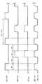
まず、本発明では上記各ガスは連続的に供給されるのではなく、図2に示すように、上記処理容器22内へSi含有ガスであるDCSガスを供給するSi含有ガス供給工程と、上記処理容器22内へ酸化性ガスであるN2 Oガスと還元性ガスであるH2 ガスとを同時に供給する酸化還元ガス供給工程とを、間欠的に交互に繰り返し行うようにする。<First embodiment>
First, a first embodiment of the method of the present invention will be described.
FIG. 2 is a diagram showing a timing chart of each gas supplied into the processing container in the first embodiment of the method of the present invention.
First, in the present invention, each of the above gases is not continuously supplied, but as shown in FIG. 2, a Si-containing gas supply step for supplying DCS gas, which is a Si-containing gas, into the processing vessel 22, The oxidation-reduction gas supply step for simultaneously supplying N2 O gas, which is an oxidizing gas, and H2 gas, which is a reducing gas, into the processing container 22 is performed alternately and repeatedly.
すなわち、図2(A)に示すようにDCSガスを供給するSi含有ガス供給工程を間欠的に行い、Si含有ガス供給工程を行っていない期間にタイミングを合わせて、図2(B)及び図2(C)に示すようにN2 OガスとH2 ガスとを同時に供給する酸化還元ガス供給工程を間欠的に行っている。ここでSi含有ガス供給工程と酸化還元ガス供給工程との間の間欠期間には、直前の工程で供給したガスの処理容器22内における残留ガスを排除するためにパージ工程を行っている。この場合、上記Si含有ガス供給工程の時間T1、酸化還元ガス供給工程の時間T2及びパージ工程の時間T3は、例えばそれぞれ10sec程度である。従って、1サイクルに要する時間は40secである。この各工程における時間は特に限定されず、処理容器22の容量にもよるが、例えば1〜180sec程度の範囲が好ましい。That is, as shown in FIG. 2 (A), the Si-containing gas supply process for supplying the DCS gas is intermittently performed, and the timing is adjusted to the period when the Si-containing gas supply process is not performed. As shown in FIG. 2 (C), an oxidation-reduction gas supply process for supplying N2 O gas and H2 gas simultaneously is performed intermittently. Here, in the intermittent period between the Si-containing gas supply process and the oxidation-reduction gas supply process, a purge process is performed to eliminate the residual gas in the processing container 22 of the gas supplied in the immediately preceding process. In this case, the time T1 of the Si-containing gas supply process, the time T2 of the oxidation-reduction gas supply process, and the time T3 of the purge process are each about 10 seconds, for example. Therefore, the time required for one cycle is 40 sec. The time in each step is not particularly limited, and is preferably in the range of, for example, about 1 to 180 seconds, although it depends on the capacity of the processing container 22.
上記Si含有ガス供給工程では、供給されたDCSガスが、成膜条件にもよるが、例えば分子状態のガスが、或いは分解したSi原子が、ウエハ表面全体に吸着することになり、この状態で酸化還元供給工程でN2 OガスとH2 ガスとが同時に供給されると、還元性ガスであるH2 ガスの作用で金属表面自体の酸化が抑制されると同時に、酸化性ガスであるN2 Oガスの作用で上記吸着していたDCSガス分子やSi原子がそれぞれ酸化されてここに酸化膜である薄いSiO2 膜が原子層レベル、或いは分子層レベルで堆積して形成されることになる。このような1サイクルの成膜操作で例えば1Å程度の厚さのSiO2 膜が形成されることになり、上記成膜操作も繰り返し行うことにより、必要な膜厚のSiO2 膜を得る。
この場合、上述のように、金属表面自体の酸化を抑制しつつこれに吸着しているSi含有ガス、或いはSi原子の酸化を促進させるためには、還元性ガスであるH2 ガスは、酸化性ガスであるN2 Oガスに対して供給量が多い状態、すなわち水素リッチな状態にしておく必要がある。In the Si-containing gas supply process, although the supplied DCS gas depends on the film forming conditions, for example, a gas in a molecular state or a decomposed Si atom is adsorbed on the entire wafer surface. When N2 O gas and H2 gas are supplied at the same time in the oxidation-reduction supply step, oxidation of the metal surface itself is suppressed by the action of H2 gas, which is a reducing gas, and at the same time, N, which is an oxidizing gas. The adsorbed DCS gas molecules and Si atoms are oxidized by the action of2 O gas, and a thin SiO2 film as an oxide film is deposited and formed at the atomic layer level or molecular layer level. Become. Such 1 will be SiO2 film cycles deposition operations, for example 1Å a thickness of approximately is formed by performing Repeat the film forming operation to obtain a SiO2 film of the required thickness.
In this case, as described above, in order to promote the oxidation of the Si-containing gas adsorbed on the metal surface itself or the Si atoms while suppressing the oxidation of the metal surface itself, the reducing gas H2 gas is oxidized. It is necessary to maintain a large supply amount with respect to N2 O gas, which is a natural gas, that is, a hydrogen rich state.
例えば本実施例では、DCSガスの流量は500sccm、N2 Oガスの流量は5sccm、H2 ガスの流量は1000sccmであり、N2 Oガスに対してH2 ガスの流量は非常に大きく設定されている。この場合、両ガスの比[酸化性ガス(N2 O)流量/還元性ガス(H2 )流量]は、1/1〜2/1000程度の範囲が望ましい。上記両ガスの比が”1/1”よりも大きくなると、酸化性ガスの作用が大きくなって金属材料表面が酸化されてしまい、好ましくない。また両ガスの比が”2/1000”よりも小さくなると、酸化性ガスが少なくなって酸化膜自体が形成されなくなってしまう。For example, in this embodiment, the flow rate of DCS gas is 500 sccm, the flow rate of N2 O gas is 5 sccm, the flow rate of H2 gas is 1000 sccm, and the flow rate of H2 gas is set to be very large relative to N2 O gas. ing. In this case, the ratio of the two gases [oxidizing gas (N2 O) flow rate / reducing gas (H2 ) flow rate] is preferably in a range of about 1/1 to 2/1000. If the ratio of the two gases is larger than “1/1”, the action of the oxidizing gas is increased, and the surface of the metal material is oxidized, which is not preferable. If the ratio of both gases is smaller than “2/1000”, the oxidizing gas is reduced and the oxide film itself is not formed.
また上記各工程における処理容器22内の圧力は、図2(D)に示されており、例えばSi含有ガス供給工程や酸化還元ガス供給工程では1Torr(133Pa)程度であり、パージ工程では略最低の圧力(バキューム)を示す。このパージ工程では、全てのガスの供給を停止した状態で真空引きを継続して行うことにより処理容器22内の残留ガスを排除するようにしてもよいし、或いは不活性ガスであるN2 ガスを供給しつつ真空引きを継続して行うことにより処理容器22内の残留ガスを排除するようにしてもよい。上記各ガス供給工程における圧力は、例えば13.3Pa(0.1Torr)〜66500Pa(500Torr)の範囲内である。またプロセス温度は、例えば50〜1000℃の範囲内である。Further, the pressure in the processing container 22 in each of the above steps is shown in FIG. 2D, and is, for example, about 1 Torr (133 Pa) in the Si-containing gas supply step and the oxidation-reduction gas supply step, and is almost the lowest in the purge step. Pressure (vacuum). In this purge process, residual gas in the processing container 22 may be removed by continuously performing evacuation with the supply of all gases stopped, or N2 gas which is an inert gas The residual gas in the processing container 22 may be excluded by continuously performing evacuation while supplying. The pressure in each said gas supply process exists in the range of 13.3 Pa (0.1 Torr)-66500 Pa (500 Torr), for example. The process temperature is, for example, in the range of 50 to 1000 ° C.
また上記DCSガスを流す際、このガスをウエハ表面に吸着させるのではなく、CVD反応領域となるようなプロセス条件を設定して、Si膜をCVD反応により堆積させるようにしてもよい。
このように、処理容器22内へSi含有ガスを供給するSi含有ガス供給工程と、処理容器22内へ酸化性ガスと還元性ガスとを同時に供給する酸化還元ガス供給工程とを、間欠的に交互に繰り返し行うようにしたので、金属表面の酸化を抑制しつつシリコン酸化膜を堆積させることができる。
従って、従来必要とされた窒化物膜等のバリヤ層を不要にできるので、半導体素子の製造工程数を削減できるのみならず、バリヤ膜に起因するストレスがなくなって素子の電気的特性も向上できる。Further, when the DCS gas is allowed to flow, the Si film may be deposited by the CVD reaction by setting process conditions for forming a CVD reaction region instead of adsorbing the gas on the wafer surface.
As described above, the Si-containing gas supply process for supplying the Si-containing gas into the processing container 22 and the redox gas supply process for simultaneously supplying the oxidizing gas and the reducing gas into the processing container 22 are intermittently performed. Since the steps are alternately repeated, the silicon oxide film can be deposited while suppressing the oxidation of the metal surface.
Accordingly, since the barrier layer such as a nitride film which has been conventionally required can be eliminated, not only the number of manufacturing steps of the semiconductor element can be reduced, but also the electrical characteristics of the element can be improved by eliminating the stress caused by the barrier film. .
ところで、目標とする厚さのSiO2 膜を形成する場合、ある程度の膜厚まで上記したような操作でSiO2 膜を形成し、その後、成膜レートを上げるために、通常のCVD成膜処理に切り替えて目標の厚さまでSiO2 膜を形成するようにしてもよい。例えば、目標膜厚が70ÅのSiO2 膜を形成する場合、上述したような成膜操作を10サイクル程度行って10Å程度のSiO2 膜を形成し、その後、成膜レートの大きなCVD成膜法に切り替えて厚さ70ÅまでSiO2 膜を形成するようにしてもよい。In the case of forming a thick SiO2 film as a target, an SiO2 film formed by the operation as described above to a certain thickness, then, in order to increase the deposition rate, conventional CVD film-forming process Alternatively, the SiO2 film may be formed to the target thickness. For example, when forming a SiO2 film having a target film thickness of 70 mm, the film forming operation as described above is performed for about 10 cycles to form a SiO2 film of about 10 mm, and then a CVD film forming method with a high film forming rate. Alternatively, the SiO2 film may be formed to a thickness of 70 mm.
<第2実施例>
次に本発明方法の第2実施例について説明する。
図3は本発明方法の第2実施例において処理容器内へ供給される各ガスのタイミングチャートを示す図である。図3では酸化性ガスとしてO2 ガスを用い、還元性ガスとしてH2 ガスを用いた場合を示している。
先の第1実施例では、酸化性ガスと還元性ガスとは常に同時に供給されるように制御したが、これに限定されず、この第2実施例では、前記酸化還元ガス供給工程の直前、または直前と直後の双方において、前記酸化性ガスの供給を停止した状態で前記還元性ガスを供給する還元ガス供給工程を行うようにしている。<Second embodiment>
Next, a second embodiment of the method of the present invention will be described.
FIG. 3 is a diagram showing a timing chart of each gas supplied into the processing container in the second embodiment of the method of the present invention. FIG. 3 shows a case where O2 gas is used as the oxidizing gas and H2 gas is used as the reducing gas.
In the previous first embodiment, the oxidizing gas and the reducing gas are controlled to be supplied at the same time. However, the present invention is not limited to this. In the second embodiment, immediately before the oxidizing and reducing gas supply step, Alternatively, a reducing gas supply step for supplying the reducing gas in a state in which the supply of the oxidizing gas is stopped is performed both immediately before and immediately after.
図3では、酸化還元ガス供給工程(時間T2で示される)の直前と直後の双方において、酸化性ガスの供給を停止した状態で還元性ガスを供給する還元性ガス供給工程をそれぞれ行っている。
ここで酸化還元ガス供給工程の直前の還元性ガス供給工程は時間T2’で示されており、直後の還元ガス供給工程は時間T2”で示されている。この時の一連のガス供給の流れは、例えば時間T3で示されるバキューム工程の後に還元性ガスであるH2 ガスの供給を先に開始し、十分な還元性ガス分圧になる様に時間T2’だけ調整してから酸化性ガスであるO2 ガスの供給を開始することになる。そして、時間T2だけO2 ガスを供給したならばO2 ガスの供給を停止し、更に、H2 ガスはその後、時間T2”だけ継続して流した後に供給を停止する。尚、ここではパージ工程で不活性ガスとして例えばN2 ガスを流しているが、このN2 ガスの供給を行わないようにしてもよく、この点は第1実施例の場合と同じである。In FIG. 3, the reducing gas supply step of supplying the reducing gas in a state where the supply of the oxidizing gas is stopped is performed both immediately before and immediately after the oxidizing and reducing gas supply step (indicated by time T2). .
Here, the reducing gas supply process immediately before the oxidation-reduction gas supply process is indicated by time T2 ′, and the reducing gas supply process immediately after is indicated by time T2 ″. A series of gas supply flows at this time For example, the supply of H2 gas, which is a reducing gas, is started first after the vacuum process indicated by
上記した各時間については、例えば時間T2は1〜100sec程度、時間T2’は1〜100sec程度、時間T2”は0〜100sec程度である。尚、時間T1、T3は第1実施例の場合と同じであり、それぞれ例えば10sec程度である。
このように、酸化還元ガス供給工程の直前に、時間T2’で示される還元ガス供給工程を行うことにより、容器内を還元性雰囲気で満たすことによって、ウエハ表面に露出している金属膜の表面が酸化することを防止することができ、この結果、最終的に作られる回路素子の電気的特性をより向上させることができる。For each of the above times, for example, time T2 is about 1 to 100 seconds, time T2 ′ is about 1 to 100 seconds, and time T2 ″ is about 0 to 100 seconds. Times T1 and T3 are the same as those in the first embodiment. The same, for example, about 10 sec.
As described above, the surface of the metal film exposed on the wafer surface is obtained by filling the inside of the container with a reducing atmosphere by performing the reducing gas supplying step indicated by time T2 ′ immediately before the oxidizing and reducing gas supplying step. As a result, the electrical characteristics of the finally produced circuit element can be further improved.
また、時間T2で示される酸化還元ガス供給工程でシリコン酸化膜を堆積した後に、時間T2”で示される還元ガス供給工程でH2 ガスを継続して供給して還元性雰囲気にすることにより、酸化膜をH2 雰囲気でアニールすることにより良質な酸化膜を得ることができる。但し、上記時間T2”で示される還元ガス供給工程は省略することができるのは、前述した通りである。また各工程における圧力関係は、第1実施例の場合と同じである。In addition, after depositing the silicon oxide film in the redox gas supply step indicated by time T2, by continuously supplying H2 gas in the reducing gas supply step indicated by time T2 ″ to make a reducing atmosphere, A good quality oxide film can be obtained by annealing the oxide film in an H2 atmosphere. However, as described above, the reducing gas supply step indicated by the time T2 ″ can be omitted. The pressure relationship in each step is the same as in the first embodiment.
上記第1及び第2実施例において説明したSiO2 膜の形成は、DRAMやフラッシュメモリ等に使用される例えば図4に示すようなポリ−メタル構造のゲート電極に対する成膜処理の時に特に有効である。すなわち、図4中において、シリコンウエハW上に、ゲート酸化膜90が形成されており、このゲート酸化膜90上に、リンドープのポリシリコン層92、タングステン窒化層(WN)94及びタングステン層(W)96を順次積層して積層構造のゲート電極を形成している。そして、このゲート電極の側面も含めて表面全体に前述したような本発明方法の成膜方法を用いてSiO2 膜よりなるサイドウォール層98を形成する。The formation of the SiO2 film described in the first and second embodiments is particularly effective at the time of film formation for a gate electrode having a poly-metal structure as shown in FIG. is there. That is, in FIG. 4, a
尚、上記実施例ではSi含有ガスとしてDCSガスを用いて場合を例にとって説明したが、これに限定されず、ジクロロシラン(DCS)、モノシラン[SiH4 ]、ジシラン[Si2 H6 ]、ヘキサクロロジシラン[Si2 Cl6 ](HCD)、ヘキサメチルジシラザン(HMDS)、テトラクロロシラン[SiHCl3 ](TCS)、ジシリルアミン(DSA)、トリシリルアミン(TSA)、ビスターシャルブチルアミノシラン(BTBAS)、[(CH3 )3 SiH](Trimethyl silane)、[(CH3 )3 SiN3 ](Trimethyl silylazide)、[SiF4 ]、[SiCl3 F]、[SiI4 ]、[Si2 F6 ]よりなる群より選択される1以上のガスを用いることができる。
またここでは酸化性ガスとしてN2 OガスまたはO2 ガスを用いた場合を例にとって説明したが、これに限定されず、N2 O、H2 O、O2 、O3 、O*(活性種)、NO、NO2 、CO2 、COよりなる群から選択される1以上のガスを用いることができる。この場合、活性種やオゾンは、イオナイザーやリモートプラズマ機構等で形成することができる。In the above-described embodiments, the case where DCS gas is used as the Si-containing gas has been described as an example. However, the present invention is not limited to this, and dichlorosilane (DCS), monosilane [SiH4 ], disilane [Si2 H6 ], hexachloro Disilane [Si2 Cl6 ] (HCD), hexamethyldisilazane (HMDS), tetrachlorosilane [SiHCl3 ] (TCS), disilylamine (DSA), trisilylamine (TSA), Vistabutyl butylaminosilane (BTBAS), [ (CH3 )3 SiH] (Trimethyl silane), [(CH3 )3 SiN3 ] (Trimethyl silylide), [SiF4 ], [SiCl3 F], [SiI4 ], [Si2 F6 ]. Using one or more gases selected from the group wear.
Further, here, the case where N2 O gas or O2 gas is used as the oxidizing gas has been described as an example. However, the present invention is not limited to this, and N2 O, H2 O, O2 , O3 , O * (active Seed), one or more gases selected from the group consisting of NO, NO2 , CO2 , CO can be used. In this case, the active species and ozone can be formed by an ionizer, a remote plasma mechanism, or the like.
またここでは還元性ガスとしてH2 ガスを用いた場合を例にとって説明したが、これに限定されず、H2 、NH3 よりなる群から選択される1以上のガスを用いることができる。
またここでは、金属材料としてタングステンを用いた場合を例にとって説明したが、これに限定されず、他の金属、例えばアルミニウム、ニッケル、コバルト、NiSi、CoSi2 、WSi2 、Cu、Fe等の場合にも本発明を適用することができる。
また成膜装置としては、バッチ式の単管構造の成膜装置に限定されず、バッチ式の2重管構造の成膜装置にも適用でき、更にはバッチ式に限定されず、ウエハを1枚ずつ処理する枚葉式の成膜装置にも本発明を適用することができる。
また被処理体としては、半導体ウエハに限定されず、ガラス基板、LCD基板等にも本発明を適用することができる。Although the case where H2 gas is used as the reducing gas has been described as an example here, the present invention is not limited to this, and one or more gases selected from the group consisting of H2 and NH3 can be used.
Also here, a case has been described using tungsten metal material as an example, not limited to this, other metals such as aluminum, nickel,cobalt, NiSi, CoSi 2, WSi 2 , Cu, if such as Fe The present invention can also be applied to.
The film forming apparatus is not limited to a batch type single tube structure film forming apparatus, but can be applied to a batch type double pipe structure film forming apparatus, and is not limited to a batch type. The present invention can also be applied to a single-wafer type film forming apparatus that processes each sheet.
The object to be processed is not limited to a semiconductor wafer, and the present invention can be applied to a glass substrate, an LCD substrate, and the like.
20 成膜装置
22 処理容器
24 ウエハボート(保持手段)
42 加熱手段
46,48,50,52 ガスノズル
60 Si含有ガス供給手段
62 酸化性ガス供給手段
64 還元性ガス供給手段
66 不活性ガス供給手段
80 制御手段
W 半導体ウエハ(被処理体)
20 Film deposition apparatus 22 Processing container 24 Wafer boat (holding means)
42 heating means 46, 48, 50, 52
Claims (19)
Translated fromJapanese前記処理容器内へSi含有ガスを供給するSi含有ガス供給工程と、
前記処理容器内へ酸化性ガスと還元性ガスとを同時に供給する酸化還元ガス供給工程とを、間欠的に交互に繰り返し行うようにしたことを特徴とする成膜方法。In a film forming method for forming a silicon oxide film on an object to be processed in which a metal surface is exposed in a processing container made evacuated,
A Si-containing gas supply step of supplying a Si-containing gas into the processing vessel;
A film forming method characterized in that the oxidation-reduction gas supply step for simultaneously supplying an oxidizing gas and a reducing gas into the processing vessel is alternately and repeatedly performed.
前記被処理体を支持する保持手段と、
Si含有ガスを供給するSi含有ガス供給手段と、
酸化性ガスを供給する酸化性ガス供給手段と、
還元性ガスを供給する還元性ガス供給手段と、
前記被処理体を加熱する加熱手段と、
装置全体を制御する制御手段と、
を有する成膜装置において、
前記制御手段は、前記処理容器内へSi含有ガスを供給する工程と、酸化性ガスと還元性ガスとを同時に供給する工程とを間欠的に交互に繰り返し行うように制御するように構成されていることを特徴とする成膜装置。A processing container which can be evacuated and can accommodate an object to be processed;
Holding means for supporting the object to be processed;
Si-containing gas supply means for supplying Si-containing gas;
An oxidizing gas supply means for supplying an oxidizing gas;
Reducing gas supply means for supplying reducing gas;
Heating means for heating the object to be processed;
Control means for controlling the entire apparatus;
In a film forming apparatus having
The control means is configured to control to intermittently and repeatedly perform the step of supplying the Si-containing gas into the processing container and the step of simultaneously supplying the oxidizing gas and the reducing gas. A film forming apparatus characterized by comprising:
前記被処理体を支持する保持手段と、
Si含有ガスを供給するSi含有ガス供給手段と、
酸化性ガスを供給する酸化性ガス供給手段と、
還元性ガスを供給する還元性ガス供給手段と、
前記被処理体を加熱する加熱手段と、
装置全体を制御する制御手段と、
を有する成膜装置を用いて成膜処理を行うに際して、
前記処理容器内へSi含有ガスを供給する工程と、酸化性ガスと還元性ガスとを同時に供給する工程とを間欠的に交互に繰り返し行うように前記成膜装置を制御するプログラムを記憶することを特徴とする記憶媒体。
A processing container which can be evacuated and can accommodate an object to be processed;
Holding means for supporting the object to be processed;
Si-containing gas supply means for supplying Si-containing gas;
An oxidizing gas supply means for supplying an oxidizing gas;
Reducing gas supply means for supplying reducing gas;
Heating means for heating the object to be processed;
Control means for controlling the entire apparatus;
When performing a film forming process using a film forming apparatus having
Storing a program for controlling the film forming apparatus so as to intermittently and alternately repeat the step of supplying the Si-containing gas into the processing vessel and the step of simultaneously supplying the oxidizing gas and the reducing gas. A storage medium characterized by the above.
Priority Applications (5)
| Application Number | Priority Date | Filing Date | Title |
|---|---|---|---|
| JP2005181282AJP4595702B2 (en) | 2004-07-15 | 2005-06-21 | Film forming method, film forming apparatus, and storage medium |
| TW094123764ATWI336108B (en) | 2004-07-15 | 2005-07-13 | Method and apparatus for forming silicon oxide film |
| US11/180,620US7651730B2 (en) | 2004-07-15 | 2005-07-14 | Method and apparatus for forming silicon oxide film |
| KR1020050063650AKR100861851B1 (en) | 2004-07-15 | 2005-07-14 | Method and apparatus for forming silicon oxide film |
| CNB2005100842886ACN100426475C (en) | 2004-07-15 | 2005-07-15 | Method and apparatus for forming silicon oxide film |
Applications Claiming Priority (2)
| Application Number | Priority Date | Filing Date | Title |
|---|---|---|---|
| JP2004209048 | 2004-07-15 | ||
| JP2005181282AJP4595702B2 (en) | 2004-07-15 | 2005-06-21 | Film forming method, film forming apparatus, and storage medium |
Publications (2)
| Publication Number | Publication Date |
|---|---|
| JP2006054432Atrue JP2006054432A (en) | 2006-02-23 |
| JP4595702B2 JP4595702B2 (en) | 2010-12-08 |
Family
ID=35798795
Family Applications (1)
| Application Number | Title | Priority Date | Filing Date |
|---|---|---|---|
| JP2005181282AExpired - LifetimeJP4595702B2 (en) | 2004-07-15 | 2005-06-21 | Film forming method, film forming apparatus, and storage medium |
Country Status (5)
| Country | Link |
|---|---|
| US (1) | US7651730B2 (en) |
| JP (1) | JP4595702B2 (en) |
| KR (1) | KR100861851B1 (en) |
| CN (1) | CN100426475C (en) |
| TW (1) | TWI336108B (en) |
Cited By (42)
| Publication number | Priority date | Publication date | Assignee | Title |
|---|---|---|---|---|
| JP2006190787A (en)* | 2005-01-05 | 2006-07-20 | Hitachi Kokusai Electric Inc | Substrate processing apparatus and semiconductor device manufacturing method |
| JP2007042884A (en)* | 2005-08-03 | 2007-02-15 | Tokyo Electron Ltd | Deposition method and apparatus therefor |
| WO2007083651A1 (en)* | 2006-01-17 | 2007-07-26 | Hitachi Kokusai Electric Inc. | Method for manufacturing semiconductor device |
| JP2008109093A (en)* | 2006-09-28 | 2008-05-08 | Tokyo Electron Ltd | Film forming method and film forming apparatus |
| JP2008533731A (en)* | 2005-03-17 | 2008-08-21 | レール・リキード−ソシエテ・アノニム・プール・レテュード・エ・レクスプロワタシオン・デ・プロセデ・ジョルジュ・クロード | Method for forming silicon oxide-containing film |
| JP2009032766A (en)* | 2007-07-25 | 2009-02-12 | Tokyo Electron Ltd | Film forming method, film forming apparatus, and storage medium |
| JP2010059546A (en)* | 2008-09-03 | 2010-03-18 | Samsung Electronics Co Ltd | Apparatus and method for forming phase change layer and method of manufacturing phase change memory device utilizing the same |
| JP2010153776A (en)* | 2008-10-29 | 2010-07-08 | Hitachi Kokusai Electric Inc | Method for manufacturing semiconductor device, and substrate processing apparatus |
| JP2010219561A (en)* | 2010-06-24 | 2010-09-30 | Hitachi Kokusai Electric Inc | Substrate processing apparatus and method of manufacturing semiconductor device |
| JP2011009752A (en)* | 2010-07-02 | 2011-01-13 | Hitachi Kokusai Electric Inc | Substrate processing apparatus, method of manufacturing semiconductor device, and semiconductor device |
| JP2011014782A (en)* | 2009-07-03 | 2011-01-20 | Renesas Electronics Corp | Method of manufacturing semiconductor device |
| JP2011023576A (en)* | 2009-07-16 | 2011-02-03 | Hitachi Kokusai Electric Inc | Method of manufacturing semiconductor device, and device for treating substrate |
| JP2011061218A (en)* | 2007-12-26 | 2011-03-24 | Hitachi Kokusai Electric Inc | Method of manufacturing semiconductor device and substrate processing apparatus |
| JP2011129877A (en)* | 2009-11-20 | 2011-06-30 | Hitachi Kokusai Electric Inc | Method of manufacturing semiconductor device, and substrate treatment apparatus |
| JP2011129879A (en)* | 2009-11-20 | 2011-06-30 | Hitachi Kokusai Electric Inc | Method of manufacturing semiconductor device, method of processing substrate, and substrate processing apparatus |
| US8076251B2 (en) | 2009-09-30 | 2011-12-13 | Hitachi Kokusai Electric, Inc. | Method of manufacturing semiconductor device, method of processing substrate and substrate processing apparatus |
| JP2012049506A (en)* | 2010-07-29 | 2012-03-08 | Tokyo Electron Ltd | Film deposition method and film deposition apparatus |
| US8168270B2 (en) | 2006-09-06 | 2012-05-01 | Tokyo Electron Limited | Film formation method and apparatus for semiconductor process |
| US20120164327A1 (en)* | 2010-12-27 | 2012-06-28 | Tokyo Electron Limited | Film-forming method and film-forming apparatus for forming silicon oxide film on tungsten film or tungsten oxide film |
| JP2012199369A (en)* | 2011-03-22 | 2012-10-18 | Hitachi Kokusai Electric Inc | Manufacturing method of semiconductor device and substrate processing apparatus |
| US8354623B2 (en) | 2007-12-07 | 2013-01-15 | Tokyo Electron Limited | Treatment apparatus, treatment method, and storage medium |
| US8431494B2 (en) | 2010-06-22 | 2013-04-30 | Tokyo Electron Limited | Film formation method and film formation apparatus |
| JP2013222725A (en)* | 2012-04-12 | 2013-10-28 | Hitachi Kokusai Electric Inc | Method for manufacturing semiconductor device, substrate processing method, substrate processing device, and program |
| JP2014064041A (en)* | 2008-10-29 | 2014-04-10 | Hitachi Kokusai Electric Inc | Semiconductor device manufacturing method, substrate processing method and substrate processing apparatus |
| US8822350B2 (en) | 2010-11-19 | 2014-09-02 | Hitachi Kokusai Electric Inc. | Method of manufacturing semiconductor device, substrate processing method and substrate processing apparatus |
| TWI462179B (en)* | 2006-09-28 | 2014-11-21 | Tokyo Electron Ltd | Film formation method and apparatus for forming silicon oxide film |
| JP2015056632A (en)* | 2013-09-13 | 2015-03-23 | 東京エレクトロン株式会社 | Method for manufacturing silicone oxide film |
| US9006116B2 (en) | 2011-06-03 | 2015-04-14 | Hitachi Kokusai Electric Inc. | Method of manufacturing semiconductor device, substrate processing method and substrate processing apparatus |
| JP2015128170A (en)* | 2006-05-23 | 2015-07-09 | エア プロダクツ アンド ケミカルズ インコーポレイテッドAir Products And Chemicals Incorporated | Silicon oxide and silicon oxynitride film, and forming method thereof, and composition for chemical vapor deposition |
| JP2015141977A (en)* | 2014-01-28 | 2015-08-03 | 東京エレクトロン株式会社 | Film forming method and film forming apparatus |
| US9123530B2 (en) | 2011-03-23 | 2015-09-01 | Hitachi Kokusai Electric Inc. | Method of manufacturing semiconductor device, substrate processing method and substrate processing apparatus |
| US9165761B2 (en) | 2011-08-25 | 2015-10-20 | Hitachi Kokusai Electric Inc. | Method for manufacturing semiconductor device, method for processing substrate, substrate processing apparatus and recording medium |
| US9425040B2 (en) | 2012-09-19 | 2016-08-23 | Tokyo Electron Limited | Method of forming laminated film and forming apparatus thereof |
| US9460913B2 (en) | 2010-12-27 | 2016-10-04 | Tokyo Electron Limited | Film-forming method for forming silicon oxide film on tungsten film or tungsten oxide film |
| US9466476B2 (en) | 2010-12-27 | 2016-10-11 | Tokyo Electron Limited | Film-forming method for forming silicon oxide film on tungsten film or tungsten oxide film |
| US9552980B2 (en) | 2013-04-22 | 2017-01-24 | Hitachi Kokusai Electric Inc. | Method of manufacturing semiconductor device, substrate processing apparatus, and recording medium |
| JP2018018896A (en)* | 2016-07-26 | 2018-02-01 | 株式会社日立国際電気 | Method of manufacturing semiconductor device, substrate processing device, and program |
| KR20190014471A (en)* | 2017-08-02 | 2019-02-12 | 도쿄엘렉트론가부시키가이샤 | Method and apparatus for forming silicon oxide film on tungsten film |
| US10607833B2 (en) | 2015-12-14 | 2020-03-31 | Kokusai Electric Corporation | Method of manufacturing semiconductor device, substrate processing apparatus, and recording medium |
| US10804100B2 (en) | 2017-09-26 | 2020-10-13 | Kokusai Electric Corporation | Method of manufacturing semiconductor device, substrate processing apparatus, and recording medium |
| US11094532B2 (en) | 2017-07-13 | 2021-08-17 | Kokusai Electric Corporation | Method of manufacturing semiconductor device, substrate processing apparatus, and recording medium |
| US11462401B2 (en) | 2013-06-03 | 2022-10-04 | Kokusai Electric Corporation | Substrate processing apparatus, method of manufacturing semiconductor device, and non-transitory computer-readable recording medium |
Families Citing this family (75)
| Publication number | Priority date | Publication date | Assignee | Title |
|---|---|---|---|---|
| US20070292974A1 (en)* | 2005-02-17 | 2007-12-20 | Hitachi Kokusai Electric Inc | Substrate Processing Method and Substrate Processing Apparatus |
| JP4899744B2 (en) | 2006-09-22 | 2012-03-21 | 東京エレクトロン株式会社 | Oxidizer for workpiece |
| US20100117203A1 (en)* | 2007-01-30 | 2010-05-13 | Aviza Technology, Inc. | Oxide-containing film formed from silicon |
| JP5616591B2 (en)* | 2008-06-20 | 2014-10-29 | 株式会社日立国際電気 | Semiconductor device manufacturing method and substrate processing apparatus |
| JP5383332B2 (en)* | 2008-08-06 | 2014-01-08 | 株式会社日立国際電気 | Substrate processing apparatus, substrate processing method, and semiconductor device manufacturing method |
| KR101583608B1 (en)* | 2009-03-24 | 2016-01-08 | 삼성전자 주식회사 | METHOD FOR FORMING SILICON OXIDE MEMBRANE USING INORGANIC SILICON precursor |
| JP5564311B2 (en) | 2009-05-19 | 2014-07-30 | 株式会社日立国際電気 | Semiconductor device manufacturing method, substrate processing apparatus, and substrate manufacturing method |
| US8895457B2 (en) | 2010-03-08 | 2014-11-25 | Hitachi Kokusai Electric Inc. | Method of manufacturing semiconductor device and substrate processing apparatus |
| US9373500B2 (en) | 2014-02-21 | 2016-06-21 | Lam Research Corporation | Plasma assisted atomic layer deposition titanium oxide for conformal encapsulation and gapfill applications |
| US9997357B2 (en) | 2010-04-15 | 2018-06-12 | Lam Research Corporation | Capped ALD films for doping fin-shaped channel regions of 3-D IC transistors |
| US9076646B2 (en) | 2010-04-15 | 2015-07-07 | Lam Research Corporation | Plasma enhanced atomic layer deposition with pulsed plasma exposure |
| US9257274B2 (en) | 2010-04-15 | 2016-02-09 | Lam Research Corporation | Gapfill of variable aspect ratio features with a composite PEALD and PECVD method |
| US9390909B2 (en) | 2013-11-07 | 2016-07-12 | Novellus Systems, Inc. | Soft landing nanolaminates for advanced patterning |
| US9892917B2 (en) | 2010-04-15 | 2018-02-13 | Lam Research Corporation | Plasma assisted atomic layer deposition of multi-layer films for patterning applications |
| US8637411B2 (en) | 2010-04-15 | 2014-01-28 | Novellus Systems, Inc. | Plasma activated conformal dielectric film deposition |
| US9611544B2 (en) | 2010-04-15 | 2017-04-04 | Novellus Systems, Inc. | Plasma activated conformal dielectric film deposition |
| US8956983B2 (en) | 2010-04-15 | 2015-02-17 | Novellus Systems, Inc. | Conformal doping via plasma activated atomic layer deposition and conformal film deposition |
| US20110256734A1 (en) | 2010-04-15 | 2011-10-20 | Hausmann Dennis M | Silicon nitride films and methods |
| CN102345111B (en)* | 2010-07-29 | 2015-03-04 | 东京毅力科创株式会社 | Film forming method and apparatus |
| US9685320B2 (en) | 2010-09-23 | 2017-06-20 | Lam Research Corporation | Methods for depositing silicon oxide |
| US9348339B2 (en)* | 2010-09-29 | 2016-05-24 | Mks Instruments, Inc. | Method and apparatus for multiple-channel pulse gas delivery system |
| US8997686B2 (en) | 2010-09-29 | 2015-04-07 | Mks Instruments, Inc. | System for and method of fast pulse gas delivery |
| US7994070B1 (en) | 2010-09-30 | 2011-08-09 | Tokyo Electron Limited | Low-temperature dielectric film formation by chemical vapor deposition |
| US10126760B2 (en) | 2011-02-25 | 2018-11-13 | Mks Instruments, Inc. | System for and method of fast pulse gas delivery |
| US10031531B2 (en)* | 2011-02-25 | 2018-07-24 | Mks Instruments, Inc. | System for and method of multiple channel fast pulse gas delivery |
| US10353408B2 (en) | 2011-02-25 | 2019-07-16 | Mks Instruments, Inc. | System for and method of fast pulse gas delivery |
| US8647993B2 (en) | 2011-04-11 | 2014-02-11 | Novellus Systems, Inc. | Methods for UV-assisted conformal film deposition |
| US20120298998A1 (en) | 2011-05-25 | 2012-11-29 | Semiconductor Energy Laboratory Co., Ltd. | Method for forming oxide semiconductor film, semiconductor device, and method for manufacturing semiconductor device |
| US20130025786A1 (en)* | 2011-07-28 | 2013-01-31 | Vladislav Davidkovich | Systems for and methods of controlling time-multiplexed deep reactive-ion etching processes |
| JP5687587B2 (en)* | 2011-09-14 | 2015-03-18 | 株式会社東芝 | Film forming method and film forming apparatus |
| US8592328B2 (en) | 2012-01-20 | 2013-11-26 | Novellus Systems, Inc. | Method for depositing a chlorine-free conformal sin film |
| WO2013134661A1 (en)* | 2012-03-09 | 2013-09-12 | Air Products And Chemicals, Inc. | Barrier materials for display devices |
| CN102820219A (en)* | 2012-07-03 | 2012-12-12 | 上海华力微电子有限公司 | Forming method of low-temperature silica film |
| CN102800569B (en)* | 2012-09-11 | 2015-11-04 | 上海华力微电子有限公司 | Based on silicon dioxide film formation method and the method, semi-conductor device manufacturing method of silane |
| KR102207992B1 (en) | 2012-10-23 | 2021-01-26 | 램 리써치 코포레이션 | Sub-saturated atomic layer deposition and conformal film deposition |
| JP6538300B2 (en) | 2012-11-08 | 2019-07-03 | ノベラス・システムズ・インコーポレーテッドNovellus Systems Incorporated | Method for depositing a film on a sensitive substrate |
| SG2013083241A (en) | 2012-11-08 | 2014-06-27 | Novellus Systems Inc | Conformal film deposition for gapfill |
| JP5925704B2 (en)* | 2013-01-17 | 2016-05-25 | 東京エレクトロン株式会社 | Silicon film forming method and apparatus therefor |
| KR20160031517A (en) | 2013-07-16 | 2016-03-22 | 쓰리엠 이노베이티브 프로퍼티즈 컴파니 | Sheet coating method |
| US9214334B2 (en) | 2014-02-18 | 2015-12-15 | Lam Research Corporation | High growth rate process for conformal aluminum nitride |
| US9478438B2 (en) | 2014-08-20 | 2016-10-25 | Lam Research Corporation | Method and apparatus to deposit pure titanium thin film at low temperature using titanium tetraiodide precursor |
| US9478411B2 (en) | 2014-08-20 | 2016-10-25 | Lam Research Corporation | Method to tune TiOx stoichiometry using atomic layer deposited Ti film to minimize contact resistance for TiOx/Ti based MIS contact scheme for CMOS |
| US9214333B1 (en) | 2014-09-24 | 2015-12-15 | Lam Research Corporation | Methods and apparatuses for uniform reduction of the in-feature wet etch rate of a silicon nitride film formed by ALD |
| US9589790B2 (en) | 2014-11-24 | 2017-03-07 | Lam Research Corporation | Method of depositing ammonia free and chlorine free conformal silicon nitride film |
| US9564312B2 (en)* | 2014-11-24 | 2017-02-07 | Lam Research Corporation | Selective inhibition in atomic layer deposition of silicon-containing films |
| US10566187B2 (en) | 2015-03-20 | 2020-02-18 | Lam Research Corporation | Ultrathin atomic layer deposition film accuracy thickness control |
| US9502238B2 (en) | 2015-04-03 | 2016-11-22 | Lam Research Corporation | Deposition of conformal films by atomic layer deposition and atomic layer etch |
| CN104911562A (en)* | 2015-05-07 | 2015-09-16 | 武汉新芯集成电路制造有限公司 | Purification method of ALD machine cavity body |
| US10526701B2 (en) | 2015-07-09 | 2020-01-07 | Lam Research Corporation | Multi-cycle ALD process for film uniformity and thickness profile modulation |
| JP6578243B2 (en)* | 2015-07-17 | 2019-09-18 | 株式会社Kokusai Electric | Gas supply nozzle, substrate processing apparatus, semiconductor device manufacturing method and program |
| US9601693B1 (en) | 2015-09-24 | 2017-03-21 | Lam Research Corporation | Method for encapsulating a chalcogenide material |
| US10410869B2 (en) | 2016-06-28 | 2019-09-10 | Applied Materials, Inc. | CVD based oxide-metal multi structure for 3D NAND memory devices |
| US9773643B1 (en) | 2016-06-30 | 2017-09-26 | Lam Research Corporation | Apparatus and method for deposition and etch in gap fill |
| US10062563B2 (en) | 2016-07-01 | 2018-08-28 | Lam Research Corporation | Selective atomic layer deposition with post-dose treatment |
| US10629435B2 (en) | 2016-07-29 | 2020-04-21 | Lam Research Corporation | Doped ALD films for semiconductor patterning applications |
| US10074543B2 (en) | 2016-08-31 | 2018-09-11 | Lam Research Corporation | High dry etch rate materials for semiconductor patterning applications |
| US10037884B2 (en) | 2016-08-31 | 2018-07-31 | Lam Research Corporation | Selective atomic layer deposition for gapfill using sacrificial underlayer |
| US9865455B1 (en) | 2016-09-07 | 2018-01-09 | Lam Research Corporation | Nitride film formed by plasma-enhanced and thermal atomic layer deposition process |
| US10454029B2 (en) | 2016-11-11 | 2019-10-22 | Lam Research Corporation | Method for reducing the wet etch rate of a sin film without damaging the underlying substrate |
| US10832908B2 (en) | 2016-11-11 | 2020-11-10 | Lam Research Corporation | Self-aligned multi-patterning process flow with ALD gapfill spacer mask |
| US10134579B2 (en) | 2016-11-14 | 2018-11-20 | Lam Research Corporation | Method for high modulus ALD SiO2 spacer |
| US10319582B2 (en)* | 2017-04-27 | 2019-06-11 | Lam Research Corporation | Methods and apparatus for depositing silicon oxide on metal layers |
| US10269559B2 (en) | 2017-09-13 | 2019-04-23 | Lam Research Corporation | Dielectric gapfill of high aspect ratio features utilizing a sacrificial etch cap layer |
| US10872762B2 (en)* | 2017-11-08 | 2020-12-22 | Taiwan Semiconductor Manufacturing Company, Ltd. | Methods of forming silicon oxide layer and semiconductor structure |
| KR102396170B1 (en)* | 2017-12-01 | 2022-05-10 | 도쿄엘렉트론가부시키가이샤 | Semiconductor device manufacturing method and film forming apparatus |
| CN112005343B (en) | 2018-03-02 | 2025-05-06 | 朗姆研究公司 | Selective deposition using hydrolysis |
| FR3086705B1 (en)* | 2018-09-27 | 2020-10-23 | Pfeiffer Vacuum | DRY TYPE PRIMARY VACUUM PUMP AND PROCESS FOR CONTROL OF THE INJECTION OF A PURGE GAS |
| KR102726216B1 (en) | 2019-05-01 | 2024-11-04 | 램 리써치 코포레이션 | Modulated atomic layer deposition |
| KR102837863B1 (en) | 2019-06-04 | 2025-07-23 | 램 리써치 코포레이션 | Polymeric protective liner for reactive ion etching during patterning |
| JP2022534793A (en) | 2019-06-07 | 2022-08-03 | ラム リサーチ コーポレーション | In situ control of film properties during atomic layer deposition |
| JP7548740B2 (en)* | 2019-07-18 | 2024-09-10 | エーエスエム・アイピー・ホールディング・ベー・フェー | Semiconductor vapor phase etching apparatus with intermediate chamber |
| CN114207184A (en) | 2019-08-06 | 2022-03-18 | 朗姆研究公司 | Thermal Atomic Layer Deposition of Silicon-Containing Films |
| TWI797640B (en)* | 2020-06-18 | 2023-04-01 | 法商液態空氣喬治斯克勞帝方法研究開發股份有限公司 | Silicon-based self-assembling monolayer compositions and surface preparation using the same |
| CN115735261A (en) | 2020-07-28 | 2023-03-03 | 朗姆研究公司 | Impurity reduction in silicon-containing films |
| US20220230855A1 (en)* | 2021-01-19 | 2022-07-21 | Changxin Memory Technologies, Inc. | Process apparatus and process method |
Citations (13)
| Publication number | Priority date | Publication date | Assignee | Title |
|---|---|---|---|---|
| JPH0411730A (en)* | 1990-04-28 | 1992-01-16 | Res Dev Corp Of Japan | Cvd method |
| JPH04349629A (en)* | 1991-05-28 | 1992-12-04 | Hitachi Ltd | Semiconductor device and its manufacturing method |
| JPH06283509A (en)* | 1993-03-26 | 1994-10-07 | Kawasaki Steel Corp | Manufacture of semiconductor device |
| JPH08288242A (en)* | 1995-02-13 | 1996-11-01 | Toshiba Corp | Method for manufacturing semiconductor device and chemical vapor deposition apparatus |
| JPH08316233A (en)* | 1994-06-21 | 1996-11-29 | Toshiba Corp | Method for manufacturing semiconductor device |
| JPH1012744A (en)* | 1996-06-24 | 1998-01-16 | Sony Corp | Method for manufacturing semiconductor device |
| JPH1187342A (en)* | 1996-11-28 | 1999-03-30 | Sony Corp | Method of forming inter-layer dielectric |
| JP2000114395A (en)* | 1998-10-09 | 2000-04-21 | Sony Corp | Semiconductor device and its manufacture |
| JP2003218106A (en)* | 2002-01-23 | 2003-07-31 | Hitachi Kokusai Electric Inc | Method for manufacturing semiconductor device |
| JP2004149925A (en)* | 2002-10-30 | 2004-05-27 | Asm Internatl Nv | Monitoring method for vaporization rate of source material in container |
| WO2005026083A2 (en)* | 2003-09-08 | 2005-03-24 | Mirus Bio Corporation | Improved delivery by labile hydrophobic modification of drugs |
| JP2005533390A (en)* | 2002-07-18 | 2005-11-04 | アヴィザ テクノロジー インコーポレイテッド | Molecular layer deposition of thin films with mixed components. |
| JP2005536055A (en)* | 2002-08-18 | 2005-11-24 | アヴィザ テクノロジー インコーポレイテッド | Low temperature deposition of silicon oxide and silicon oxynitride |
Family Cites Families (9)
| Publication number | Priority date | Publication date | Assignee | Title |
|---|---|---|---|---|
| US5721155A (en)* | 1995-02-13 | 1998-02-24 | Lg Semicon Co., Ltd. | Method for forming a via contact of a semiconductor device |
| JP3105770B2 (en)* | 1995-09-29 | 2000-11-06 | 日本電気株式会社 | Method for manufacturing semiconductor device |
| JPH09246257A (en) | 1996-03-08 | 1997-09-19 | Hitachi Ltd | Semiconductor manufacturing apparatus and gas discharge method |
| JP3644880B2 (en) | 2000-06-20 | 2005-05-11 | 東京エレクトロン株式会社 | Vertical heat treatment equipment |
| US6846516B2 (en)* | 2002-04-08 | 2005-01-25 | Applied Materials, Inc. | Multiple precursor cyclical deposition system |
| US7097886B2 (en)* | 2002-12-13 | 2006-08-29 | Applied Materials, Inc. | Deposition process for high aspect ratio trenches |
| KR100470973B1 (en)* | 2003-02-26 | 2005-03-10 | 삼성전자주식회사 | High density plasma chemical vapor deposition process |
| US7399388B2 (en)* | 2003-07-25 | 2008-07-15 | Applied Materials, Inc. | Sequential gas flow oxide deposition technique |
| US20050181633A1 (en)* | 2004-02-17 | 2005-08-18 | Hochberg Arthur K. | Precursors for depositing silicon-containing films and processes thereof |
- 2005
- 2005-06-21JPJP2005181282Apatent/JP4595702B2/ennot_activeExpired - Lifetime
- 2005-07-13TWTW094123764Apatent/TWI336108B/ennot_activeIP Right Cessation
- 2005-07-14KRKR1020050063650Apatent/KR100861851B1/ennot_activeExpired - Lifetime
- 2005-07-14USUS11/180,620patent/US7651730B2/enactiveActive
- 2005-07-15CNCNB2005100842886Apatent/CN100426475C/ennot_activeExpired - Lifetime
Patent Citations (13)
| Publication number | Priority date | Publication date | Assignee | Title |
|---|---|---|---|---|
| JPH0411730A (en)* | 1990-04-28 | 1992-01-16 | Res Dev Corp Of Japan | Cvd method |
| JPH04349629A (en)* | 1991-05-28 | 1992-12-04 | Hitachi Ltd | Semiconductor device and its manufacturing method |
| JPH06283509A (en)* | 1993-03-26 | 1994-10-07 | Kawasaki Steel Corp | Manufacture of semiconductor device |
| JPH08316233A (en)* | 1994-06-21 | 1996-11-29 | Toshiba Corp | Method for manufacturing semiconductor device |
| JPH08288242A (en)* | 1995-02-13 | 1996-11-01 | Toshiba Corp | Method for manufacturing semiconductor device and chemical vapor deposition apparatus |
| JPH1012744A (en)* | 1996-06-24 | 1998-01-16 | Sony Corp | Method for manufacturing semiconductor device |
| JPH1187342A (en)* | 1996-11-28 | 1999-03-30 | Sony Corp | Method of forming inter-layer dielectric |
| JP2000114395A (en)* | 1998-10-09 | 2000-04-21 | Sony Corp | Semiconductor device and its manufacture |
| JP2003218106A (en)* | 2002-01-23 | 2003-07-31 | Hitachi Kokusai Electric Inc | Method for manufacturing semiconductor device |
| JP2005533390A (en)* | 2002-07-18 | 2005-11-04 | アヴィザ テクノロジー インコーポレイテッド | Molecular layer deposition of thin films with mixed components. |
| JP2005536055A (en)* | 2002-08-18 | 2005-11-24 | アヴィザ テクノロジー インコーポレイテッド | Low temperature deposition of silicon oxide and silicon oxynitride |
| JP2004149925A (en)* | 2002-10-30 | 2004-05-27 | Asm Internatl Nv | Monitoring method for vaporization rate of source material in container |
| WO2005026083A2 (en)* | 2003-09-08 | 2005-03-24 | Mirus Bio Corporation | Improved delivery by labile hydrophobic modification of drugs |
Cited By (69)
| Publication number | Priority date | Publication date | Assignee | Title |
|---|---|---|---|---|
| JP2006190787A (en)* | 2005-01-05 | 2006-07-20 | Hitachi Kokusai Electric Inc | Substrate processing apparatus and semiconductor device manufacturing method |
| JP2008533731A (en)* | 2005-03-17 | 2008-08-21 | レール・リキード−ソシエテ・アノニム・プール・レテュード・エ・レクスプロワタシオン・デ・プロセデ・ジョルジュ・クロード | Method for forming silicon oxide-containing film |
| JP2013070077A (en)* | 2005-03-17 | 2013-04-18 | L'air Liquide Societe Anonyme Pour L'etude Et L'exploitation Des Procedes Georges Claude | Formation method of silicon oxide containing film |
| JP2007042884A (en)* | 2005-08-03 | 2007-02-15 | Tokyo Electron Ltd | Deposition method and apparatus therefor |
| US8058184B2 (en) | 2006-01-17 | 2011-11-15 | Hitachi Kokusai Electric Inc. | Semiconductor device producing method |
| JP2011176330A (en)* | 2006-01-17 | 2011-09-08 | Hitachi Kokusai Electric Inc | Method of producing semiconductor device, and substrate processing apparatus |
| JPWO2007083651A1 (en)* | 2006-01-17 | 2009-06-11 | 株式会社日立国際電気 | Manufacturing method of semiconductor device |
| WO2007083651A1 (en)* | 2006-01-17 | 2007-07-26 | Hitachi Kokusai Electric Inc. | Method for manufacturing semiconductor device |
| US7767594B2 (en) | 2006-01-17 | 2010-08-03 | Hitachi Kokusai Electric Inc. | Semiconductor device producing method |
| JP4896041B2 (en)* | 2006-01-17 | 2012-03-14 | 株式会社日立国際電気 | Manufacturing method of semiconductor device |
| JP2015128170A (en)* | 2006-05-23 | 2015-07-09 | エア プロダクツ アンド ケミカルズ インコーポレイテッドAir Products And Chemicals Incorporated | Silicon oxide and silicon oxynitride film, and forming method thereof, and composition for chemical vapor deposition |
| US8168270B2 (en) | 2006-09-06 | 2012-05-01 | Tokyo Electron Limited | Film formation method and apparatus for semiconductor process |
| JP2008109093A (en)* | 2006-09-28 | 2008-05-08 | Tokyo Electron Ltd | Film forming method and film forming apparatus |
| TWI462179B (en)* | 2006-09-28 | 2014-11-21 | Tokyo Electron Ltd | Film formation method and apparatus for forming silicon oxide film |
| JP2009032766A (en)* | 2007-07-25 | 2009-02-12 | Tokyo Electron Ltd | Film forming method, film forming apparatus, and storage medium |
| US8354623B2 (en) | 2007-12-07 | 2013-01-15 | Tokyo Electron Limited | Treatment apparatus, treatment method, and storage medium |
| JP2011061218A (en)* | 2007-12-26 | 2011-03-24 | Hitachi Kokusai Electric Inc | Method of manufacturing semiconductor device and substrate processing apparatus |
| US8980679B2 (en) | 2008-09-03 | 2015-03-17 | Samsung Electronics Co., Ltd. | Apparatus and methods for forming phase change layer and method of manufacturing phase change memory device |
| JP2010059546A (en)* | 2008-09-03 | 2010-03-18 | Samsung Electronics Co Ltd | Apparatus and method for forming phase change layer and method of manufacturing phase change memory device utilizing the same |
| US8367557B2 (en) | 2008-10-29 | 2013-02-05 | Hitachi Kokosai Electric, Inc. | Method of forming an insulation film having low impurity concentrations |
| US8809204B2 (en) | 2008-10-29 | 2014-08-19 | Hitachi Kokusai Electric Inc. | Method of manufacturing semiconductor device and substrate processing apparatus |
| JP2014064041A (en)* | 2008-10-29 | 2014-04-10 | Hitachi Kokusai Electric Inc | Semiconductor device manufacturing method, substrate processing method and substrate processing apparatus |
| US9011601B2 (en) | 2008-10-29 | 2015-04-21 | Hitachi Kokusai Electric Inc. | Substrate processing apparatus |
| US9269566B2 (en) | 2008-10-29 | 2016-02-23 | Hitachi Kokusai Electric Inc. | Substrate processing apparatus |
| JP2010153776A (en)* | 2008-10-29 | 2010-07-08 | Hitachi Kokusai Electric Inc | Method for manufacturing semiconductor device, and substrate processing apparatus |
| JP2011014782A (en)* | 2009-07-03 | 2011-01-20 | Renesas Electronics Corp | Method of manufacturing semiconductor device |
| JP2011023576A (en)* | 2009-07-16 | 2011-02-03 | Hitachi Kokusai Electric Inc | Method of manufacturing semiconductor device, and device for treating substrate |
| US8415258B2 (en) | 2009-09-30 | 2013-04-09 | Hitachi Kokusai Electric Inc. | Method of manufacturing semiconductor device, method of processing substrate and substrate processing apparatus |
| US8076251B2 (en) | 2009-09-30 | 2011-12-13 | Hitachi Kokusai Electric, Inc. | Method of manufacturing semiconductor device, method of processing substrate and substrate processing apparatus |
| US9039838B2 (en) | 2009-11-20 | 2015-05-26 | Hitachi Kokusai Electric Inc. | Method of manufacturing semiconductor device and substrate processing apparatus |
| US8252701B2 (en) | 2009-11-20 | 2012-08-28 | Hitachi-Kokusai Electric Inc. | Method of manufacturing semiconductor device, method of processing substrate, and substrate processing apparatus |
| JP2011129879A (en)* | 2009-11-20 | 2011-06-30 | Hitachi Kokusai Electric Inc | Method of manufacturing semiconductor device, method of processing substrate, and substrate processing apparatus |
| US9966251B2 (en) | 2009-11-20 | 2018-05-08 | Hitachi Kokusai Electric Inc. | Method of manufacturing semiconductor device and substrate processing apparatus |
| US8202809B2 (en) | 2009-11-20 | 2012-06-19 | Hitachi Kokusai Electric Inc. | Method of manufacturing semiconductor device, method of processing substrate, and substrate processing apparatus |
| US9966252B2 (en) | 2009-11-20 | 2018-05-08 | Hitachi Kokusai Electric Inc. | Method of manufacturing semiconductor device and substrate processing apparatus |
| JP2011129877A (en)* | 2009-11-20 | 2011-06-30 | Hitachi Kokusai Electric Inc | Method of manufacturing semiconductor device, and substrate treatment apparatus |
| US8431494B2 (en) | 2010-06-22 | 2013-04-30 | Tokyo Electron Limited | Film formation method and film formation apparatus |
| JP2010219561A (en)* | 2010-06-24 | 2010-09-30 | Hitachi Kokusai Electric Inc | Substrate processing apparatus and method of manufacturing semiconductor device |
| JP2011009752A (en)* | 2010-07-02 | 2011-01-13 | Hitachi Kokusai Electric Inc | Substrate processing apparatus, method of manufacturing semiconductor device, and semiconductor device |
| US8658247B2 (en) | 2010-07-29 | 2014-02-25 | Tokyo Electron Limited | Film deposition method |
| JP2012049506A (en)* | 2010-07-29 | 2012-03-08 | Tokyo Electron Ltd | Film deposition method and film deposition apparatus |
| KR101434345B1 (en) | 2010-07-29 | 2014-08-26 | 도쿄엘렉트론가부시키가이샤 | Film deposition method and film deposition apparatus |
| US20120190215A1 (en)* | 2010-07-29 | 2012-07-26 | Tokyo Electron Limited | Film deposition method and film deposition apparatus |
| US8822350B2 (en) | 2010-11-19 | 2014-09-02 | Hitachi Kokusai Electric Inc. | Method of manufacturing semiconductor device, substrate processing method and substrate processing apparatus |
| US9466476B2 (en) | 2010-12-27 | 2016-10-11 | Tokyo Electron Limited | Film-forming method for forming silicon oxide film on tungsten film or tungsten oxide film |
| US9460913B2 (en) | 2010-12-27 | 2016-10-04 | Tokyo Electron Limited | Film-forming method for forming silicon oxide film on tungsten film or tungsten oxide film |
| US20140199839A1 (en)* | 2010-12-27 | 2014-07-17 | Tokyo Electron Limited | Film-forming method for forming silicon oxide film on tungsten film or tungsten oxide film |
| KR101759157B1 (en)* | 2010-12-27 | 2017-07-18 | 도쿄엘렉트론가부시키가이샤 | Film-forming method for forming silicon oxide film |
| JP2012138500A (en)* | 2010-12-27 | 2012-07-19 | Tokyo Electron Ltd | Method for forming silicon oxide film on tungsten film or tungsten oxide film and film forming device |
| US20120164327A1 (en)* | 2010-12-27 | 2012-06-28 | Tokyo Electron Limited | Film-forming method and film-forming apparatus for forming silicon oxide film on tungsten film or tungsten oxide film |
| JP2012199369A (en)* | 2011-03-22 | 2012-10-18 | Hitachi Kokusai Electric Inc | Manufacturing method of semiconductor device and substrate processing apparatus |
| US9761437B2 (en) | 2011-03-23 | 2017-09-12 | Hitachi Kokusai Electric Inc. | Method of manufacturing semiconductor device, substrate processing method and substrate processing apparatus |
| US9123530B2 (en) | 2011-03-23 | 2015-09-01 | Hitachi Kokusai Electric Inc. | Method of manufacturing semiconductor device, substrate processing method and substrate processing apparatus |
| US9006116B2 (en) | 2011-06-03 | 2015-04-14 | Hitachi Kokusai Electric Inc. | Method of manufacturing semiconductor device, substrate processing method and substrate processing apparatus |
| US9165761B2 (en) | 2011-08-25 | 2015-10-20 | Hitachi Kokusai Electric Inc. | Method for manufacturing semiconductor device, method for processing substrate, substrate processing apparatus and recording medium |
| US9384961B2 (en) | 2011-08-25 | 2016-07-05 | Hitachi Kokusai Electric Inc. | Method for manufacturing semiconductor device, method for processing substrate, substrate processing apparatus and recording medium |
| JP2013222725A (en)* | 2012-04-12 | 2013-10-28 | Hitachi Kokusai Electric Inc | Method for manufacturing semiconductor device, substrate processing method, substrate processing device, and program |
| US9425040B2 (en) | 2012-09-19 | 2016-08-23 | Tokyo Electron Limited | Method of forming laminated film and forming apparatus thereof |
| US9552980B2 (en) | 2013-04-22 | 2017-01-24 | Hitachi Kokusai Electric Inc. | Method of manufacturing semiconductor device, substrate processing apparatus, and recording medium |
| US11462401B2 (en) | 2013-06-03 | 2022-10-04 | Kokusai Electric Corporation | Substrate processing apparatus, method of manufacturing semiconductor device, and non-transitory computer-readable recording medium |
| JP2015056632A (en)* | 2013-09-13 | 2015-03-23 | 東京エレクトロン株式会社 | Method for manufacturing silicone oxide film |
| JP2015141977A (en)* | 2014-01-28 | 2015-08-03 | 東京エレクトロン株式会社 | Film forming method and film forming apparatus |
| US10607833B2 (en) | 2015-12-14 | 2020-03-31 | Kokusai Electric Corporation | Method of manufacturing semiconductor device, substrate processing apparatus, and recording medium |
| JP2018018896A (en)* | 2016-07-26 | 2018-02-01 | 株式会社日立国際電気 | Method of manufacturing semiconductor device, substrate processing device, and program |
| US11094532B2 (en) | 2017-07-13 | 2021-08-17 | Kokusai Electric Corporation | Method of manufacturing semiconductor device, substrate processing apparatus, and recording medium |
| JP2019029582A (en)* | 2017-08-02 | 2019-02-21 | 東京エレクトロン株式会社 | Method and apparatus for forming silicon oxide film on tungsten film |
| KR20190014471A (en)* | 2017-08-02 | 2019-02-12 | 도쿄엘렉트론가부시키가이샤 | Method and apparatus for forming silicon oxide film on tungsten film |
| KR102295441B1 (en) | 2017-08-02 | 2021-08-27 | 도쿄엘렉트론가부시키가이샤 | Method and apparatus for forming silicon oxide film on tungsten film |
| US10804100B2 (en) | 2017-09-26 | 2020-10-13 | Kokusai Electric Corporation | Method of manufacturing semiconductor device, substrate processing apparatus, and recording medium |
Also Published As
| Publication number | Publication date |
|---|---|
| KR20060050163A (en) | 2006-05-19 |
| CN100426475C (en) | 2008-10-15 |
| TWI336108B (en) | 2011-01-11 |
| US20060032442A1 (en) | 2006-02-16 |
| CN1734726A (en) | 2006-02-15 |
| JP4595702B2 (en) | 2010-12-08 |
| TW200625444A (en) | 2006-07-16 |
| US7651730B2 (en) | 2010-01-26 |
| KR100861851B1 (en) | 2008-10-07 |
Similar Documents
| Publication | Publication Date | Title |
|---|---|---|
| JP4595702B2 (en) | Film forming method, film forming apparatus, and storage medium | |
| KR101498960B1 (en) | Thin film formation method and film formation apparatus | |
| US9269566B2 (en) | Substrate processing apparatus | |
| JP4396547B2 (en) | Film forming method, film forming apparatus, and storage medium | |
| JP5572447B2 (en) | Semiconductor device manufacturing method, substrate processing method, and substrate processing apparatus | |
| JP5467007B2 (en) | Semiconductor device manufacturing method and substrate processing apparatus | |
| CN112309830B (en) | Semiconductor device manufacturing method, substrate processing device and recording medium | |
| JP5541223B2 (en) | Film forming method and film forming apparatus | |
| JP5651451B2 (en) | Semiconductor device manufacturing method, substrate processing method, and substrate processing apparatus | |
| JP7598992B2 (en) | Processing method, semiconductor device manufacturing method, processing device, and program | |
| JP2019212740A (en) | Cleaning method, semiconductor device manufacturing method, substrate processing apparatus, and program | |
| JP5982045B2 (en) | Semiconductor device manufacturing method, substrate processing method, substrate processing apparatus, and gas supply system | |
| JP2006066884A (en) | Film forming method, film forming apparatus, and storage medium | |
| JP2007035740A (en) | Film deposition method, film deposition equipment, and storage medium | |
| JP7305013B2 (en) | Substrate processing method, semiconductor device manufacturing method, substrate processing apparatus, and program | |
| JP7135190B2 (en) | Semiconductor device manufacturing method, substrate processing method, substrate processing apparatus, and program | |
| JP5051180B2 (en) | Deposition method | |
| JP2025101076A (en) | Processing method, semiconductor device manufacturing method, processing device, and program |
Legal Events
| Date | Code | Title | Description |
|---|---|---|---|
| A977 | Report on retrieval | Free format text:JAPANESE INTERMEDIATE CODE: A971007 Effective date:20070705 | |
| A131 | Notification of reasons for refusal | Free format text:JAPANESE INTERMEDIATE CODE: A131 Effective date:20080415 | |
| A521 | Request for written amendment filed | Free format text:JAPANESE INTERMEDIATE CODE: A523 Effective date:20080613 | |
| A131 | Notification of reasons for refusal | Free format text:JAPANESE INTERMEDIATE CODE: A131 Effective date:20090428 | |
| A521 | Request for written amendment filed | Free format text:JAPANESE INTERMEDIATE CODE: A523 Effective date:20090619 | |
| A131 | Notification of reasons for refusal | Free format text:JAPANESE INTERMEDIATE CODE: A131 Effective date:20100601 | |
| A521 | Request for written amendment filed | Free format text:JAPANESE INTERMEDIATE CODE: A523 Effective date:20100722 | |
| TRDD | Decision of grant or rejection written | ||
| A01 | Written decision to grant a patent or to grant a registration (utility model) | Free format text:JAPANESE INTERMEDIATE CODE: A01 Effective date:20100824 | |
| A01 | Written decision to grant a patent or to grant a registration (utility model) | Free format text:JAPANESE INTERMEDIATE CODE: A01 | |
| A61 | First payment of annual fees (during grant procedure) | Free format text:JAPANESE INTERMEDIATE CODE: A61 Effective date:20100906 | |
| R150 | Certificate of patent or registration of utility model | Ref document number:4595702 Country of ref document:JP Free format text:JAPANESE INTERMEDIATE CODE: R150 Free format text:JAPANESE INTERMEDIATE CODE: R150 | |
| FPAY | Renewal fee payment (event date is renewal date of database) | Free format text:PAYMENT UNTIL: 20131001 Year of fee payment:3 | |
| R250 | Receipt of annual fees | Free format text:JAPANESE INTERMEDIATE CODE: R250 | |
| R250 | Receipt of annual fees | Free format text:JAPANESE INTERMEDIATE CODE: R250 | |
| R250 | Receipt of annual fees | Free format text:JAPANESE INTERMEDIATE CODE: R250 | |
| R250 | Receipt of annual fees | Free format text:JAPANESE INTERMEDIATE CODE: R250 | |
| R250 | Receipt of annual fees | Free format text:JAPANESE INTERMEDIATE CODE: R250 | |
| R250 | Receipt of annual fees | Free format text:JAPANESE INTERMEDIATE CODE: R250 | |
| R250 | Receipt of annual fees | Free format text:JAPANESE INTERMEDIATE CODE: R250 | |
| R250 | Receipt of annual fees | Free format text:JAPANESE INTERMEDIATE CODE: R250 | |
| EXPY | Cancellation because of completion of term |