JP2006052324A - Organic material, organic electroluminescent element, and display device - Google Patents
Organic material, organic electroluminescent element, and display deviceDownload PDFInfo
- Publication number
- JP2006052324A JP2006052324AJP2004235124AJP2004235124AJP2006052324AJP 2006052324 AJP2006052324 AJP 2006052324AJP 2004235124 AJP2004235124 AJP 2004235124AJP 2004235124 AJP2004235124 AJP 2004235124AJP 2006052324 AJP2006052324 AJP 2006052324A
- Authority
- JP
- Japan
- Prior art keywords
- group
- carbon atoms
- substituted
- less carbon
- unsubstituted
- Prior art date
- Legal status (The legal status is an assumption and is not a legal conclusion. Google has not performed a legal analysis and makes no representation as to the accuracy of the status listed.)
- Pending
Links
- 239000011368organic materialSubstances0.000titleclaimsabstractdescription67
- WDECIBYCCFPHNR-UHFFFAOYSA-NchryseneChemical compoundC1=CC=CC2=CC=C3C4=CC=CC=C4C=CC3=C21WDECIBYCCFPHNR-UHFFFAOYSA-N0.000claimsabstractdescription43
- 239000010410layerSubstances0.000claimsdescription129
- 239000012044organic layerSubstances0.000claimsdescription55
- 125000004432carbon atomChemical groupC*0.000claimsdescription42
- 125000000623heterocyclic groupChemical group0.000claimsdescription23
- 239000000758substrateSubstances0.000claimsdescription22
- UFWIBTONFRDIAS-UHFFFAOYSA-NNaphthaleneChemical compoundC1=CC=CC2=CC=CC=C21UFWIBTONFRDIAS-UHFFFAOYSA-N0.000claimsdescription20
- 125000003118aryl groupChemical group0.000claimsdescription20
- UHOVQNZJYSORNB-UHFFFAOYSA-NBenzeneChemical compoundC1=CC=CC=C1UHOVQNZJYSORNB-UHFFFAOYSA-N0.000claimsdescription13
- MWPLVEDNUUSJAV-UHFFFAOYSA-NanthraceneChemical compoundC1=CC=CC2=CC3=CC=CC=C3C=C21MWPLVEDNUUSJAV-UHFFFAOYSA-N0.000claimsdescription13
- 125000002915carbonyl groupChemical group[*:2]C([*:1])=O0.000claimsdescription13
- GVEPBJHOBDJJJI-UHFFFAOYSA-NfluoranthreneNatural productsC1=CC(C2=CC=CC=C22)=C3C2=CC=CC3=C1GVEPBJHOBDJJJI-UHFFFAOYSA-N0.000claimsdescription13
- 239000002019doping agentSubstances0.000claimsdescription11
- 125000000217alkyl groupChemical group0.000claimsdescription10
- BBEAQIROQSPTKN-UHFFFAOYSA-NpyreneChemical compoundC1=CC=C2C=CC3=CC=CC4=CC=C1C2=C43BBEAQIROQSPTKN-UHFFFAOYSA-N0.000claimsdescription10
- 125000003342alkenyl groupChemical group0.000claimsdescription6
- 125000003545alkoxy groupChemical group0.000claimsdescription6
- 125000004185ester groupChemical group0.000claimsdescription6
- 125000002080perylenyl groupChemical groupC1(=CC=C2C=CC=C3C4=CC=CC5=CC=CC(C1=C23)=C45)*0.000claimsdescription6
- CSHWQDPOILHKBI-UHFFFAOYSA-NperyreneNatural productsC1=CC(C2=CC=CC=3C2=C2C=CC=3)=C3C2=CC=CC3=C1CSHWQDPOILHKBI-UHFFFAOYSA-N0.000claimsdescription6
- 125000003808silyl groupChemical group[H][Si]([H])([H])[*]0.000claimsdescription6
- 229910052736halogenInorganic materials0.000claimsdescription5
- 150000002367halogensChemical class0.000claimsdescription5
- 125000002887hydroxy groupChemical group[H]O*0.000claimsdescription5
- 125000000449nitro groupChemical group[O-][N+](*)=O0.000claimsdescription5
- 125000004093cyano groupChemical group*C#N0.000claimsdescription4
- 239000001257hydrogenSubstances0.000claimsdescription4
- 229910052739hydrogenInorganic materials0.000claimsdescription4
- 125000004435hydrogen atomChemical class[H]*0.000claimsdescription4
- 238000006467substitution reactionMethods0.000claimsdescription4
- 239000000463materialSubstances0.000description42
- 238000000034methodMethods0.000description26
- YXFVVABEGXRONW-UHFFFAOYSA-NTolueneChemical compoundCC1=CC=CC=C1YXFVVABEGXRONW-UHFFFAOYSA-N0.000description24
- 150000001875compoundsChemical class0.000description24
- 239000010408filmSubstances0.000description23
- 230000005525hole transportEffects0.000description18
- -1styryl alleneChemical class0.000description18
- 238000005401electroluminescenceMethods0.000description17
- 238000006243chemical reactionMethods0.000description16
- 230000015572biosynthetic processEffects0.000description15
- 238000002347injectionMethods0.000description15
- 239000007924injectionSubstances0.000description15
- 238000003786synthesis reactionMethods0.000description14
- IJGRMHOSHXDMSA-UHFFFAOYSA-NAtomic nitrogenChemical compoundN#NIJGRMHOSHXDMSA-UHFFFAOYSA-N0.000description12
- KDLHZDBZIXYQEI-UHFFFAOYSA-NPalladiumChemical compound[Pd]KDLHZDBZIXYQEI-UHFFFAOYSA-N0.000description12
- VYPSYNLAJGMNEJ-UHFFFAOYSA-NSilicium dioxideChemical compoundO=[Si]=OVYPSYNLAJGMNEJ-UHFFFAOYSA-N0.000description12
- VLKZOEOYAKHREP-UHFFFAOYSA-Nn-HexaneChemical compoundCCCCCCVLKZOEOYAKHREP-UHFFFAOYSA-N0.000description9
- 229910052751metalInorganic materials0.000description8
- 239000002184metalSubstances0.000description8
- 229910052757nitrogenInorganic materials0.000description8
- NFHFRUOZVGFOOS-UHFFFAOYSA-Npalladium;triphenylphosphaneChemical compound[Pd].C1=CC=CC=C1P(C=1C=CC=CC=1)C1=CC=CC=C1.C1=CC=CC=C1P(C=1C=CC=CC=1)C1=CC=CC=C1.C1=CC=CC=C1P(C=1C=CC=CC=1)C1=CC=CC=C1.C1=CC=CC=C1P(C=1C=CC=CC=1)C1=CC=CC=C1NFHFRUOZVGFOOS-UHFFFAOYSA-N0.000description8
- TVIVIEFSHFOWTE-UHFFFAOYSA-Ktri(quinolin-8-yloxy)alumaneChemical compound[Al+3].C1=CN=C2C([O-])=CC=CC2=C1.C1=CN=C2C([O-])=CC=CC2=C1.C1=CN=C2C([O-])=CC=CC2=C1TVIVIEFSHFOWTE-UHFFFAOYSA-K0.000description7
- IAZDPXIOMUYVGZ-UHFFFAOYSA-NDimethylsulphoxideChemical compoundCS(C)=OIAZDPXIOMUYVGZ-UHFFFAOYSA-N0.000description6
- 239000003054catalystSubstances0.000description6
- 239000007787solidSubstances0.000description6
- 125000001424substituent groupChemical group0.000description6
- 239000010409thin filmSubstances0.000description6
- 238000000151depositionMethods0.000description5
- 230000008021depositionEffects0.000description5
- 238000011156evaluationMethods0.000description5
- 239000011521glassSubstances0.000description5
- 150000002894organic compoundsChemical class0.000description5
- 238000000746purificationMethods0.000description5
- 239000000377silicon dioxideSubstances0.000description5
- 239000000243solutionSubstances0.000description5
- 238000001771vacuum depositionMethods0.000description5
- KAKZBPTYRLMSJV-UHFFFAOYSA-NButadieneChemical compoundC=CC=CKAKZBPTYRLMSJV-UHFFFAOYSA-N0.000description4
- CSNNHWWHGAXBCP-UHFFFAOYSA-LMagnesium sulfateChemical compound[Mg+2].[O-][S+2]([O-])([O-])[O-]CSNNHWWHGAXBCP-UHFFFAOYSA-L0.000description4
- DZBUGLKDJFMEHC-UHFFFAOYSA-NacridineChemical compoundC1=CC=CC2=CC3=CC=CC=C3N=C21DZBUGLKDJFMEHC-UHFFFAOYSA-N0.000description4
- QVGXLLKOCUKJST-UHFFFAOYSA-Natomic oxygenChemical compound[O]QVGXLLKOCUKJST-UHFFFAOYSA-N0.000description4
- 239000011651chromiumSubstances0.000description4
- 150000001846chrysenesChemical class0.000description4
- 230000000052comparative effectEffects0.000description4
- 239000011159matrix materialSubstances0.000description4
- 150000002739metalsChemical class0.000description4
- 239000000203mixtureSubstances0.000description4
- IBHBKWKFFTZAHE-UHFFFAOYSA-Nn-[4-[4-(n-naphthalen-1-ylanilino)phenyl]phenyl]-n-phenylnaphthalen-1-amineChemical compoundC1=CC=CC=C1N(C=1C2=CC=CC=C2C=CC=1)C1=CC=C(C=2C=CC(=CC=2)N(C=2C=CC=CC=2)C=2C3=CC=CC=C3C=CC=2)C=C1IBHBKWKFFTZAHE-UHFFFAOYSA-N0.000description4
- QJGQUHMNIGDVPM-UHFFFAOYSA-Nnitrogen groupChemical group[N]QJGQUHMNIGDVPM-UHFFFAOYSA-N0.000description4
- 239000001301oxygenSubstances0.000description4
- 229910052760oxygenInorganic materials0.000description4
- 229910052763palladiumInorganic materials0.000description4
- YNPNZTXNASCQKK-UHFFFAOYSA-NphenanthreneChemical compoundC1=CC=C2C3=CC=CC=C3C=CC2=C1YNPNZTXNASCQKK-UHFFFAOYSA-N0.000description4
- 238000003756stirringMethods0.000description4
- 239000000126substanceSubstances0.000description4
- 230000002194synthesizing effectEffects0.000description4
- XLYOFNOQVPJJNP-UHFFFAOYSA-NwaterSubstancesOXLYOFNOQVPJJNP-UHFFFAOYSA-N0.000description4
- DIVZFUBWFAOMCW-UHFFFAOYSA-N4-n-(3-methylphenyl)-1-n,1-n-bis[4-(n-(3-methylphenyl)anilino)phenyl]-4-n-phenylbenzene-1,4-diamineChemical compoundCC1=CC=CC(N(C=2C=CC=CC=2)C=2C=CC(=CC=2)N(C=2C=CC(=CC=2)N(C=2C=CC=CC=2)C=2C=C(C)C=CC=2)C=2C=CC(=CC=2)N(C=2C=CC=CC=2)C=2C=C(C)C=CC=2)=C1DIVZFUBWFAOMCW-UHFFFAOYSA-N0.000description3
- PJANXHGTPQOBST-VAWYXSNFSA-NStilbeneNatural productsC=1C=CC=CC=1/C=C/C1=CC=CC=C1PJANXHGTPQOBST-VAWYXSNFSA-N0.000description3
- 229910045601alloyInorganic materials0.000description3
- 239000000956alloySubstances0.000description3
- 150000001454anthracenesChemical class0.000description3
- 239000007864aqueous solutionSubstances0.000description3
- 125000005578chrysene groupChemical group0.000description3
- 239000010949copperSubstances0.000description3
- 230000000694effectsEffects0.000description3
- 150000002391heterocyclic compoundsChemical class0.000description3
- RAXXELZNTBOGNW-UHFFFAOYSA-NimidazoleNatural productsC1=CNC=N1RAXXELZNTBOGNW-UHFFFAOYSA-N0.000description3
- 238000010030laminatingMethods0.000description3
- 239000011777magnesiumSubstances0.000description3
- 238000004519manufacturing processMethods0.000description3
- 239000011259mixed solutionSubstances0.000description3
- 239000012046mixed solventSubstances0.000description3
- 238000010992refluxMethods0.000description3
- 239000011347resinSubstances0.000description3
- 229920005989resinPolymers0.000description3
- 235000012239silicon dioxideNutrition0.000description3
- 239000011734sodiumSubstances0.000description3
- 239000002904solventSubstances0.000description3
- PJANXHGTPQOBST-UHFFFAOYSA-NstilbeneChemical compoundC=1C=CC=CC=1C=CC1=CC=CC=C1PJANXHGTPQOBST-UHFFFAOYSA-N0.000description3
- 235000021286stilbenesNutrition0.000description3
- 239000012780transparent materialSubstances0.000description3
- UWRZIZXBOLBCON-VOTSOKGWSA-N(e)-2-phenylethenamineChemical compoundN\C=C\C1=CC=CC=C1UWRZIZXBOLBCON-VOTSOKGWSA-N0.000description2
- 2380000051601H NMR spectroscopyMethods0.000description2
- YBYIRNPNPLQARY-UHFFFAOYSA-N1H-indeneChemical compoundC1=CC=C2CC=CC2=C1YBYIRNPNPLQARY-UHFFFAOYSA-N0.000description2
- PJZDEYKZSZWFPX-UHFFFAOYSA-N2,6-dibromonaphthaleneChemical compoundC1=C(Br)C=CC2=CC(Br)=CC=C21PJZDEYKZSZWFPX-UHFFFAOYSA-N0.000description2
- GOLORTLGFDVFDW-UHFFFAOYSA-N3-(1h-benzimidazol-2-yl)-7-(diethylamino)chromen-2-oneChemical compoundC1=CC=C2NC(C3=CC4=CC=C(C=C4OC3=O)N(CC)CC)=NC2=C1GOLORTLGFDVFDW-UHFFFAOYSA-N0.000description2
- RULVBMDEPWAFIN-UHFFFAOYSA-N6,12-dibromochryseneChemical compoundC1=CC=C2C(Br)=CC3=C(C=CC=C4)C4=C(Br)C=C3C2=C1RULVBMDEPWAFIN-UHFFFAOYSA-N0.000description2
- CSCPPACGZOOCGX-UHFFFAOYSA-NAcetoneChemical compoundCC(C)=OCSCPPACGZOOCGX-UHFFFAOYSA-N0.000description2
- XKRFYHLGVUSROY-UHFFFAOYSA-NArgonChemical compound[Ar]XKRFYHLGVUSROY-UHFFFAOYSA-N0.000description2
- GZCIGLXUFVFQAY-UHFFFAOYSA-NBrC=1C=C2C=3C=CC=CC=3C(=CC2=C2C=CC=CC=12)C1=CC=CC2=CC=CC=C12Chemical compoundBrC=1C=C2C=3C=CC=CC=3C(=CC2=C2C=CC=CC=12)C1=CC=CC2=CC=CC=C12GZCIGLXUFVFQAY-UHFFFAOYSA-N0.000description2
- CURLTUGMZLYLDI-UHFFFAOYSA-NCarbon dioxideChemical compoundO=C=OCURLTUGMZLYLDI-UHFFFAOYSA-N0.000description2
- VYZAMTAEIAYCRO-UHFFFAOYSA-NChromiumChemical compound[Cr]VYZAMTAEIAYCRO-UHFFFAOYSA-N0.000description2
- RYGMFSIKBFXOCR-UHFFFAOYSA-NCopperChemical compound[Cu]RYGMFSIKBFXOCR-UHFFFAOYSA-N0.000description2
- LFQSCWFLJHTTHZ-UHFFFAOYSA-NEthanolChemical compoundCCOLFQSCWFLJHTTHZ-UHFFFAOYSA-N0.000description2
- WHXSMMKQMYFTQS-UHFFFAOYSA-NLithiumChemical compound[Li]WHXSMMKQMYFTQS-UHFFFAOYSA-N0.000description2
- FYYHWMGAXLPEAU-UHFFFAOYSA-NMagnesiumChemical compound[Mg]FYYHWMGAXLPEAU-UHFFFAOYSA-N0.000description2
- 238000005481NMR spectroscopyMethods0.000description2
- ZCQWOFVYLHDMMC-UHFFFAOYSA-NOxazoleChemical compoundC1=COC=N1ZCQWOFVYLHDMMC-UHFFFAOYSA-N0.000description2
- KYQCOXFCLRTKLS-UHFFFAOYSA-NPyrazineChemical compoundC1=CN=CC=N1KYQCOXFCLRTKLS-UHFFFAOYSA-N0.000description2
- SMWDFEZZVXVKRB-UHFFFAOYSA-NQuinolineChemical compoundN1=CC=CC2=CC=CC=C21SMWDFEZZVXVKRB-UHFFFAOYSA-N0.000description2
- 229910052782aluminiumInorganic materials0.000description2
- XAGFODPZIPBFFR-UHFFFAOYSA-NaluminiumChemical compound[Al]XAGFODPZIPBFFR-UHFFFAOYSA-N0.000description2
- 229910052792caesiumInorganic materials0.000description2
- TVFDJXOCXUVLDH-UHFFFAOYSA-Ncaesium atomChemical compound[Cs]TVFDJXOCXUVLDH-UHFFFAOYSA-N0.000description2
- 239000011575calciumSubstances0.000description2
- 229910052804chromiumInorganic materials0.000description2
- 229910052802copperInorganic materials0.000description2
- VPUGDVKSAQVFFS-UHFFFAOYSA-NcoroneneChemical compoundC1=C(C2=C34)C=CC3=CC=C(C=C3)C4=C4C3=CC=C(C=C3)C4=C2C3=C1VPUGDVKSAQVFFS-UHFFFAOYSA-N0.000description2
- 125000006165cyclic alkyl groupChemical group0.000description2
- 230000005684electric fieldEffects0.000description2
- 238000000295emission spectrumMethods0.000description2
- 238000000434field desorption mass spectrometryMethods0.000description2
- YLQWCDOCJODRMT-UHFFFAOYSA-Nfluoren-9-oneChemical compoundC1=CC=C2C(=O)C3=CC=CC=C3C2=C1YLQWCDOCJODRMT-UHFFFAOYSA-N0.000description2
- 239000010931goldSubstances0.000description2
- 230000006872improvementEffects0.000description2
- AMGQUBHHOARCQH-UHFFFAOYSA-Nindium;oxotinChemical compound[In].[Sn]=OAMGQUBHHOARCQH-UHFFFAOYSA-N0.000description2
- 239000004973liquid crystal related substanceSubstances0.000description2
- 229910052744lithiumInorganic materials0.000description2
- 229910052749magnesiumInorganic materials0.000description2
- 229910052943magnesium sulfateInorganic materials0.000description2
- 235000019341magnesium sulphateNutrition0.000description2
- HUMMCEUVDBVXTQ-UHFFFAOYSA-Nnaphthalen-1-ylboronic acidChemical compoundC1=CC=C2C(B(O)O)=CC=CC2=C1HUMMCEUVDBVXTQ-UHFFFAOYSA-N0.000description2
- WCPAKWJPBJAGKN-UHFFFAOYSA-NoxadiazoleChemical compoundC1=CON=N1WCPAKWJPBJAGKN-UHFFFAOYSA-N0.000description2
- 230000003647oxidationEffects0.000description2
- 238000007254oxidation reactionMethods0.000description2
- 230000035699permeabilityEffects0.000description2
- GBROPGWFBFCKAG-UHFFFAOYSA-NpiceneChemical compoundC1=CC2=C3C=CC=CC3=CC=C2C2=C1C1=CC=CC=C1C=C2GBROPGWFBFCKAG-UHFFFAOYSA-N0.000description2
- 229920003229poly(methyl methacrylate)Polymers0.000description2
- 229920000139polyethylene terephthalatePolymers0.000description2
- 239000005020polyethylene terephthalateSubstances0.000description2
- 239000004926polymethyl methacrylateSubstances0.000description2
- 150000004032porphyrinsChemical class0.000description2
- SCVFZCLFOSHCOH-UHFFFAOYSA-Mpotassium acetateChemical compound[K+].CC([O-])=OSCVFZCLFOSHCOH-UHFFFAOYSA-M0.000description2
- 239000000047productSubstances0.000description2
- 239000010453quartzSubstances0.000description2
- 239000011541reaction mixtureSubstances0.000description2
- 230000006798recombinationEffects0.000description2
- 238000005215recombinationMethods0.000description2
- 230000004044responseEffects0.000description2
- 238000000926separation methodMethods0.000description2
- 238000004544sputter depositionMethods0.000description2
- 238000003860storageMethods0.000description2
- 125000005504styryl groupChemical group0.000description2
- 150000003852triazolesChemical class0.000description2
- 238000007738vacuum evaporationMethods0.000description2
- 238000007740vapor depositionMethods0.000description2
- NAWXUBYGYWOOIX-SFHVURJKSA-N(2s)-2-[[4-[2-(2,4-diaminoquinazolin-6-yl)ethyl]benzoyl]amino]-4-methylidenepentanedioic acidChemical compoundC1=CC2=NC(N)=NC(N)=C2C=C1CCC1=CC=C(C(=O)N[C@@H](CC(=C)C(O)=O)C(O)=O)C=C1NAWXUBYGYWOOIX-SFHVURJKSA-N0.000description1
- GEYOCULIXLDCMW-UHFFFAOYSA-N1,2-phenylenediamineChemical compoundNC1=CC=CC=C1NGEYOCULIXLDCMW-UHFFFAOYSA-N0.000description1
- APQXWKHOGQFGTB-UHFFFAOYSA-N1-ethenyl-9h-carbazoleChemical classC12=CC=CC=C2NC2=C1C=CC=C2C=CAPQXWKHOGQFGTB-UHFFFAOYSA-N0.000description1
- SJADXKHSFIMCRC-UHFFFAOYSA-N1-n,1-n,4-n,4-n-tetrakis(4-methylphenyl)benzene-1,4-diamineChemical compoundC1=CC(C)=CC=C1N(C=1C=CC(=CC=1)N(C=1C=CC(C)=CC=1)C=1C=CC(C)=CC=1)C1=CC=C(C)C=C1SJADXKHSFIMCRC-UHFFFAOYSA-N0.000description1
- BPRGLVVFWRNXEP-UHFFFAOYSA-N2,6-dibromoanthraceneChemical compoundC1=C(Br)C=CC2=CC3=CC(Br)=CC=C3C=C21BPRGLVVFWRNXEP-UHFFFAOYSA-N0.000description1
- FEYDZHNIIMENOB-UHFFFAOYSA-N2,6-dibromopyridineChemical compoundBrC1=CC=CC(Br)=N1FEYDZHNIIMENOB-UHFFFAOYSA-N0.000description1
- HONWGFNQCPRRFM-UHFFFAOYSA-N2-n-(3-methylphenyl)-1-n,1-n,2-n-triphenylbenzene-1,2-diamineChemical compoundCC1=CC=CC(N(C=2C=CC=CC=2)C=2C(=CC=CC=2)N(C=2C=CC=CC=2)C=2C=CC=CC=2)=C1HONWGFNQCPRRFM-UHFFFAOYSA-N0.000description1
- ACWRSZKNNOJCJE-UHFFFAOYSA-N2-n-naphthalen-1-yl-2-n-phenylbenzene-1,2-diamineChemical compoundNC1=CC=CC=C1N(C=1C2=CC=CC=C2C=CC=1)C1=CC=CC=C1ACWRSZKNNOJCJE-UHFFFAOYSA-N0.000description1
- MGADZUXDNSDTHW-UHFFFAOYSA-N2H-pyranChemical compoundC1OC=CC=C1MGADZUXDNSDTHW-UHFFFAOYSA-N0.000description1
- RMTFQLKKBBWGAH-UHFFFAOYSA-N4-methyl-n-(4-methylphenyl)-n-[4-(2-phenylethenyl)phenyl]anilineChemical compoundC1=CC(C)=CC=C1N(C=1C=CC(C=CC=2C=CC=CC=2)=CC=1)C1=CC=C(C)C=C1RMTFQLKKBBWGAH-UHFFFAOYSA-N0.000description1
- FAAAKDIORRDGMS-UHFFFAOYSA-N6-bromochryseneChemical compoundC1=CC=C2C(Br)=CC3=C(C=CC=C4)C4=CC=C3C2=C1FAAAKDIORRDGMS-UHFFFAOYSA-N0.000description1
- CFNMUZCFSDMZPQ-GHXNOFRVSA-N7-[(z)-3-methyl-4-(4-methyl-5-oxo-2h-furan-2-yl)but-2-enoxy]chromen-2-oneChemical compoundC=1C=C2C=CC(=O)OC2=CC=1OC/C=C(/C)CC1OC(=O)C(C)=C1CFNMUZCFSDMZPQ-GHXNOFRVSA-N0.000description1
- BRUOAURMAFDGLP-UHFFFAOYSA-N9,10-dibromoanthraceneChemical compoundC1=CC=C2C(Br)=C(C=CC=C3)C3=C(Br)C2=C1BRUOAURMAFDGLP-UHFFFAOYSA-N0.000description1
- VIZUPBYFLORCRA-UHFFFAOYSA-N9,10-dinaphthalen-2-ylanthraceneChemical compoundC12=CC=CC=C2C(C2=CC3=CC=CC=C3C=C2)=C(C=CC=C2)C2=C1C1=CC=C(C=CC=C2)C2=C1VIZUPBYFLORCRA-UHFFFAOYSA-N0.000description1
- VIJYEGDOKCKUOL-UHFFFAOYSA-N9-phenylcarbazoleChemical compoundC1=CC=CC=C1N1C2=CC=CC=C2C2=CC=CC=C21VIJYEGDOKCKUOL-UHFFFAOYSA-N0.000description1
- OYPRJOBELJOOCE-UHFFFAOYSA-NCalciumChemical compound[Ca]OYPRJOBELJOOCE-UHFFFAOYSA-N0.000description1
- 238000003747Grignard reactionMethods0.000description1
- 229910018068Li 2 OInorganic materials0.000description1
- ZOKXTWBITQBERF-UHFFFAOYSA-NMolybdenumChemical compound[Mo]ZOKXTWBITQBERF-UHFFFAOYSA-N0.000description1
- PCNDJXKNXGMECE-UHFFFAOYSA-NPhenazineNatural productsC1=CC=CC2=NC3=CC=CC=C3N=C21PCNDJXKNXGMECE-UHFFFAOYSA-N0.000description1
- 229910004298SiO 2Inorganic materials0.000description1
- BQCADISMDOOEFD-UHFFFAOYSA-NSilverChemical compound[Ag]BQCADISMDOOEFD-UHFFFAOYSA-N0.000description1
- 229910001128Sn alloyInorganic materials0.000description1
- 229910006404SnO 2Inorganic materials0.000description1
- PMZURENOXWZQFD-UHFFFAOYSA-LSodium SulfateChemical compound[Na+].[Na+].[O-]S([O-])(=O)=OPMZURENOXWZQFD-UHFFFAOYSA-L0.000description1
- 238000006069Suzuki reaction reactionMethods0.000description1
- SLGBZMMZGDRARJ-UHFFFAOYSA-NTriphenyleneNatural productsC1=CC=C2C3=CC=CC=C3C3=CC=CC=C3C2=C1SLGBZMMZGDRARJ-UHFFFAOYSA-N0.000description1
- 239000007983Tris bufferSubstances0.000description1
- 238000006887Ullmann reactionMethods0.000description1
- XLOMVQKBTHCTTD-UHFFFAOYSA-NZinc monoxideChemical compound[Zn]=OXLOMVQKBTHCTTD-UHFFFAOYSA-N0.000description1
- XGQBAQHNKOWRLL-UHFFFAOYSA-N[Eu].C(C1=CC=CC=C1)(=O)C(C(C1=CC=CC=C1)=O)C1=C(C(=NC2=C3N=CC=CC3=CC=C12)C(C(C1=CC=CC=C1)=O)C(C1=CC=CC=C1)=O)C(C(C1=CC=CC=C1)=O)C(C1=CC=CC=C1)=OChemical compound[Eu].C(C1=CC=CC=C1)(=O)C(C(C1=CC=CC=C1)=O)C1=C(C(=NC2=C3N=CC=CC3=CC=C12)C(C(C1=CC=CC=C1)=O)C(C1=CC=CC=C1)=O)C(C(C1=CC=CC=C1)=O)C(C1=CC=CC=C1)=OXGQBAQHNKOWRLL-UHFFFAOYSA-N0.000description1
- SQFPKRNUGBRTAR-UHFFFAOYSA-NacephenanthryleneChemical groupC1=CC(C=C2)=C3C2=CC2=CC=CC=C2C3=C1SQFPKRNUGBRTAR-UHFFFAOYSA-N0.000description1
- TWVGAEQMWFGWDX-UHFFFAOYSA-Nacetylene;thiopheneChemical groupC#C.C=1C=CSC=1TWVGAEQMWFGWDX-UHFFFAOYSA-N0.000description1
- 125000003172aldehyde groupChemical group0.000description1
- 229910052783alkali metalInorganic materials0.000description1
- 150000001340alkali metalsChemical class0.000description1
- 229910052784alkaline earth metalInorganic materials0.000description1
- 150000001342alkaline earth metalsChemical class0.000description1
- PNEYBMLMFCGWSK-UHFFFAOYSA-Naluminium oxideInorganic materials[O-2].[O-2].[O-2].[Al+3].[Al+3]PNEYBMLMFCGWSK-UHFFFAOYSA-N0.000description1
- APLQAVQJYBLXDR-UHFFFAOYSA-Naluminum quinolineChemical compound[Al+3].N1=CC=CC2=CC=CC=C12.N1=CC=CC2=CC=CC=C12.N1=CC=CC2=CC=CC=C12APLQAVQJYBLXDR-UHFFFAOYSA-N0.000description1
- 150000001448anilinesChemical class0.000description1
- 125000005577anthracene groupChemical group0.000description1
- 229910052787antimonyInorganic materials0.000description1
- WATWJIUSRGPENY-UHFFFAOYSA-Nantimony atomChemical compound[Sb]WATWJIUSRGPENY-UHFFFAOYSA-N0.000description1
- 229910052786argonInorganic materials0.000description1
- 150000004982aromatic aminesChemical class0.000description1
- 150000001502aryl halidesChemical class0.000description1
- 229910052788bariumInorganic materials0.000description1
- DSAJWYNOEDNPEQ-UHFFFAOYSA-Nbarium atomChemical compound[Ba]DSAJWYNOEDNPEQ-UHFFFAOYSA-N0.000description1
- 229910052790berylliumInorganic materials0.000description1
- ATBAMAFKBVZNFJ-UHFFFAOYSA-Nberyllium atomChemical compound[Be]ATBAMAFKBVZNFJ-UHFFFAOYSA-N0.000description1
- 230000005540biological transmissionEffects0.000description1
- 239000006227byproductSubstances0.000description1
- 229910052791calciumInorganic materials0.000description1
- 239000001569carbon dioxideSubstances0.000description1
- 229910002092carbon dioxideInorganic materials0.000description1
- 125000003178carboxy groupChemical group[H]OC(*)=O0.000description1
- QFZNDWQAHYCUKB-UHFFFAOYSA-Nchrysen-1-ylboronic acidChemical compoundC1=CC2=C3C=CC=CC3=CC=C2C2=C1C(B(O)O)=CC=C2QFZNDWQAHYCUKB-UHFFFAOYSA-N0.000description1
- 238000004040coloringMethods0.000description1
- 239000000470constituentSubstances0.000description1
- 150000004696coordination complexChemical class0.000description1
- 230000008878couplingEffects0.000description1
- 238000010168coupling processMethods0.000description1
- 238000005859coupling reactionMethods0.000description1
- 238000002425crystallisationMethods0.000description1
- 230000008025crystallizationEffects0.000description1
- 238000000354decomposition reactionMethods0.000description1
- 230000006866deteriorationEffects0.000description1
- ZOCHARZZJNPSEU-UHFFFAOYSA-NdiboronChemical compoundB#BZOCHARZZJNPSEU-UHFFFAOYSA-N0.000description1
- AKUNKIJLSDQFLS-UHFFFAOYSA-Mdicesium;hydroxideChemical compound[OH-].[Cs+].[Cs+]AKUNKIJLSDQFLS-UHFFFAOYSA-M0.000description1
- XUCJHNOBJLKZNU-UHFFFAOYSA-Mdilithium;hydroxideChemical compound[Li+].[Li+].[OH-]XUCJHNOBJLKZNU-UHFFFAOYSA-M0.000description1
- 238000004821distillationMethods0.000description1
- 239000000975dyeSubstances0.000description1
- 239000007772electrode materialSubstances0.000description1
- 230000005284excitationEffects0.000description1
- 230000001747exhibiting effectEffects0.000description1
- 239000007850fluorescent dyeSubstances0.000description1
- 229920001109fluorescent polymerPolymers0.000description1
- 239000011888foilSubstances0.000description1
- 239000007789gasSubstances0.000description1
- PCHJSUWPFVWCPO-UHFFFAOYSA-NgoldChemical compound[Au]PCHJSUWPFVWCPO-UHFFFAOYSA-N0.000description1
- 229910052737goldInorganic materials0.000description1
- 125000001072heteroaryl groupChemical group0.000description1
- 150000007857hydrazonesChemical class0.000description1
- 229910052738indiumInorganic materials0.000description1
- APFVFJFRJDLVQX-UHFFFAOYSA-Nindium atomChemical compound[In]APFVFJFRJDLVQX-UHFFFAOYSA-N0.000description1
- 239000011261inert gasSubstances0.000description1
- 150000002484inorganic compoundsChemical class0.000description1
- 229910010272inorganic materialInorganic materials0.000description1
- 230000003993interactionEffects0.000description1
- 125000000468ketone groupChemical group0.000description1
- 230000000873masking effectEffects0.000description1
- 239000007769metal materialSubstances0.000description1
- 125000005395methacrylic acid groupChemical group0.000description1
- 229910052750molybdenumInorganic materials0.000description1
- 239000011733molybdenumSubstances0.000description1
- 239000000178monomerSubstances0.000description1
- DCZNSJVFOQPSRV-UHFFFAOYSA-Nn,n-diphenyl-4-[4-(n-phenylanilino)phenyl]anilineChemical groupC1=CC=CC=C1N(C=1C=CC(=CC=1)C=1C=CC(=CC=1)N(C=1C=CC=CC=1)C=1C=CC=CC=1)C1=CC=CC=C1DCZNSJVFOQPSRV-UHFFFAOYSA-N0.000description1
- 150000002790naphthalenesChemical class0.000description1
- LKKPNUDVOYAOBB-UHFFFAOYSA-NnaphthalocyanineChemical compoundN1C(N=C2C3=CC4=CC=CC=C4C=C3C(N=C3C4=CC5=CC=CC=C5C=C4C(=N4)N3)=N2)=C(C=C2C(C=CC=C2)=C2)C2=C1N=C1C2=CC3=CC=CC=C3C=C2C4=N1LKKPNUDVOYAOBB-UHFFFAOYSA-N0.000description1
- 125000001624naphthyl groupChemical group0.000description1
- 125000002560nitrile groupChemical group0.000description1
- 230000003287optical effectEffects0.000description1
- NRZWYNLTFLDQQX-UHFFFAOYSA-Np-tert-AmylphenolChemical compoundCCC(C)(C)C1=CC=C(O)C=C1NRZWYNLTFLDQQX-UHFFFAOYSA-N0.000description1
- SLIUAWYAILUBJU-UHFFFAOYSA-NpentaceneChemical compoundC1=CC=CC2=CC3=CC4=CC5=CC=CC=C5C=C4C=C3C=C21SLIUAWYAILUBJU-UHFFFAOYSA-N0.000description1
- 125000001997phenyl groupChemical group[H]C1=C([H])C([H])=C(*)C([H])=C1[H]0.000description1
- IEQIEDJGQAUEQZ-UHFFFAOYSA-NphthalocyanineChemical classN1C(N=C2C3=CC=CC=C3C(N=C3C4=CC=CC=C4C(=N4)N3)=N2)=C(C=CC=C2)C2=C1N=C1C2=CC=CC=C2C4=N1IEQIEDJGQAUEQZ-UHFFFAOYSA-N0.000description1
- 238000005268plasma chemical vapour depositionMethods0.000description1
- 229920000553poly(phenylenevinylene)Polymers0.000description1
- 229920000548poly(silane) polymerPolymers0.000description1
- 229920005668polycarbonate resinPolymers0.000description1
- 239000004431polycarbonate resinSubstances0.000description1
- 229920000728polyesterPolymers0.000description1
- 239000011112polyethylene naphthalateSubstances0.000description1
- 229920000642polymerPolymers0.000description1
- 235000011056potassium acetateNutrition0.000description1
- 150000003220pyrenesChemical class0.000description1
- YGDICLRMNDWZAK-UHFFFAOYSA-Nquinolin-3-ylboronic acidChemical compoundC1=CC=CC2=CC(B(O)O)=CN=C21YGDICLRMNDWZAK-UHFFFAOYSA-N0.000description1
- 238000001953recrystallisationMethods0.000description1
- 238000001226reprecipitationMethods0.000description1
- 238000011160researchMethods0.000description1
- 238000012827research and developmentMethods0.000description1
- 239000013557residual solventSubstances0.000description1
- 229910052709silverInorganic materials0.000description1
- 239000004332silverSubstances0.000description1
- 229910052938sodium sulfateInorganic materials0.000description1
- 235000011152sodium sulphateNutrition0.000description1
- 238000004528spin coatingMethods0.000description1
- 238000000859sublimationMethods0.000description1
- 230000008022sublimationEffects0.000description1
- 238000004381surface treatmentMethods0.000description1
- 238000001308synthesis methodMethods0.000description1
- IFLREYGFSNHWGE-UHFFFAOYSA-NtetraceneChemical compoundC1=CC=CC2=CC3=CC4=CC=CC=C4C=C3C=C21IFLREYGFSNHWGE-UHFFFAOYSA-N0.000description1
- 150000003518tetracenesChemical class0.000description1
- YNHJECZULSZAQK-UHFFFAOYSA-NtetraphenylporphyrinChemical compoundC1=CC(C(=C2C=CC(N2)=C(C=2C=CC=CC=2)C=2C=CC(N=2)=C(C=2C=CC=CC=2)C2=CC=C3N2)C=2C=CC=CC=2)=NC1=C3C1=CC=CC=C1YNHJECZULSZAQK-UHFFFAOYSA-N0.000description1
- 150000003577thiophenesChemical class0.000description1
- XOLBLPGZBRYERU-UHFFFAOYSA-Ntin dioxideChemical compoundO=[Sn]=OXOLBLPGZBRYERU-UHFFFAOYSA-N0.000description1
- 229910052723transition metalInorganic materials0.000description1
- 150000003624transition metalsChemical class0.000description1
- 238000002834transmittanceMethods0.000description1
- ODHXBMXNKOYIBV-UHFFFAOYSA-NtriphenylamineChemical compoundC1=CC=CC=C1N(C=1C=CC=CC=1)C1=CC=CC=C1ODHXBMXNKOYIBV-UHFFFAOYSA-N0.000description1
- 125000005580triphenylene groupChemical group0.000description1
- WFKWXMTUELFFGS-UHFFFAOYSA-NtungstenChemical compound[W]WFKWXMTUELFFGS-UHFFFAOYSA-N0.000description1
- 229910052721tungstenInorganic materials0.000description1
- 239000010937tungstenSubstances0.000description1
- YVTHLONGBIQYBO-UHFFFAOYSA-Nzinc indium(3+) oxygen(2-)Chemical compound[O--].[Zn++].[In+3]YVTHLONGBIQYBO-UHFFFAOYSA-N0.000description1
Images

Landscapes
- Electroluminescent Light Sources (AREA)
Abstract
Description
Translated fromJapanese本発明は、有機材料、これを用いた有機電界発光素子、およびこれを用いた表示装置に関する。 The present invention relates to an organic material, an organic electroluminescent element using the same, and a display device using the same.
近年、軽量で高効率のフラットパネルディスプレイが、例えばコンピュータやテレビジョンの画面表示用として盛んに研究、開発されている。最も代表的な表示装置であるブラウン管(CRT)は、輝度が高く、色再現性が良いため、現在ディスプレイとして最も多く使われているが、嵩高く、重く、また消費電力も高いという問題がある。 In recent years, light and highly efficient flat panel displays have been actively researched and developed, for example, as screen displays for computers and televisions. The most representative display device, a cathode ray tube (CRT), is currently used most frequently as a display because of its high brightness and good color reproducibility. However, it is bulky, heavy and has high power consumption. .
また、軽量で高効率のフラットパネルディスプレイとして、アクティブマトリックス駆動などの液晶ディスプレイが商品化されている。しかしながら、液晶ディスプレイは、視野角が狭く、また、自発光でないため周囲が暗い環境下ではバックライトの消費電力が大きいことや、今後実用化が期待されている高精細度の高速ビデオ信号に対して十分な応答性能を有しない等の問題点がある。特に、大画面サイズのディスプレイを製造することは困難であり、そのコストが高い等の課題もある。 In addition, liquid crystal displays such as active matrix driving have been commercialized as lightweight and highly efficient flat panel displays. However, the liquid crystal display has a narrow viewing angle and is not self-luminous, so the backlight consumes a lot of power in an environment where the surroundings are dark, and the high-definition high-speed video signal expected to be put to practical use in the future. In addition, there are problems such as not having sufficient response performance. In particular, it is difficult to produce a display with a large screen size, and there are problems such as high cost.
そこで、これらの諸課題を解決する可能性のあるフラットパネルディスプレイとして、最近、有機材料を用いた有機電界発光素子(いわゆる有機EL素子)が注目されている。即ち、発光材料として有機化合物を用いることにより、自発光で、応答速度が高速であり、視野角依存性の無いフラットパネルディスプレイの実現が期待されている。 Thus, recently, an organic electroluminescent element (so-called organic EL element) using an organic material has attracted attention as a flat panel display that can solve these problems. That is, by using an organic compound as a light-emitting material, it is expected to realize a flat panel display that is self-luminous, has a high response speed, and has no viewing angle dependency.
一般的な有機電界発光素子の構成は、透光性の陽極と金属材料からなる陰極との間に、電流を流すことによって発光する有機材料を含む有機層を狭持してなる。この有機電界発光素子の歴史的背景としては、まず、有機層を正孔輸送性材料からなる薄膜と電子輸送性材料からなる薄膜との2層構造とし、この有機層を挟む状態で設けられた陽極および陰極から、有機層中にそれぞれ注入された正孔(ホール)と電子とが再結合することにより発光する素子構造が開発された(例えば、下記非特許文献1参照)。 A general configuration of an organic electroluminescent element is formed by sandwiching an organic layer containing an organic material that emits light when an electric current is passed between a light-transmitting anode and a cathode made of a metal material. As the historical background of this organic electroluminescent device, first, the organic layer was provided with a two-layer structure of a thin film made of a hole transporting material and a thin film made of an electron transporting material, and sandwiched between the organic layers. An element structure has been developed that emits light by recombination of holes and electrons injected into the organic layer from the anode and the cathode, respectively (for example, see Non-Patent
その後、有機層が、正孔輸送材料、発光材料、電子輸送材料の3層構造からなる有機電界発光素子が開発され(例えば、下記非特許文献2参照)、さらに電子輸送材料中に発光材料を含ませた素子構造などが開発された(例えば、下記非特許文献3参照)。これらの研究により、有機電界発光素子において、低電圧で、高輝度の発光の可能性が検証され、近年、研究開発が非常に活発に行われている。 Thereafter, an organic electroluminescent device having an organic layer having a three-layer structure of a hole transport material, a light emitting material, and an electron transport material was developed (for example, see Non-Patent Document 2 below). The element structure etc. which were included were developed (for example, refer the following nonpatent literature 3). These studies have verified the possibility of light emission at low voltage and high brightness in organic electroluminescent devices, and research and development has been very active in recent years.
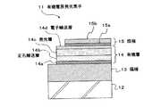
図2は、このような有機電界発光素子の一構成例を示す断面図である。この図に示す有機電界発光素子1は、例えばガラス等からなる透明な基板2上に設けられており、基板2上に設けられたITO(Indium Tin Oxide:透明電極)からなる陽極3、陽極3上に設けられた有機層4、および有機層4上に設けられた陰極5により構成されている。有機層4は、陽極3側から、正孔注入層4a、正孔輸送層4bおよび電子輸送性の発光層4cを順次積層させた構成を有している。この有機電界発光素子1では、陰極5から注入された電子と陽極3から注入された正孔とが発光層4cにて再結合し、この再結合の際に生じる光が陽極3を介して基板2側から取り出される。 FIG. 2 is a cross-sectional view showing a configuration example of such an organic electroluminescent element. The organic
有機電界発光素子1としては、このような構成を有するものの他に、基板側から順に、陰極、有機層、陽極を順次積層した構成のものや、上方に位置する電極(陰極または陽極としての上部電極)を透明材料で構成することによって、基板と反対側の上部電極側から光を取り出すようにした、いわゆる上面発光型の有機電界発光素子もある。 As the organic
特に、基板上に薄膜トランジスタ(Thin Film Transistor:TFT)を設けてなるアクティブマトリックス型の表示装置においては、TFTが形成された基板上に上面発光型の有機電界発光素子を設けた、いわゆるTAC(Top Emitting Adoptive Current drive )構造とすることが、発光部の開口率を向上させる上で有利になる。 In particular, in an active matrix type display device in which a thin film transistor (TFT) is provided on a substrate, a so-called TAC (Top) in which a top emission organic electroluminescence element is provided on a substrate on which a TFT is formed. Emitting Adoptive Current drive) structure is advantageous in improving the aperture ratio of the light emitting portion.
そして、このような構成の有機電界発光素子における有機材料については様々な検討がなされており、特に青色発色材料についてはスチリルアレンもしくはアントラセン誘導体について改良が進められてきた(例えば、下記非特許文献4参照)。 Various studies have been made on the organic material in the organic electroluminescence device having such a configuration, and in particular, improvement has been made on styryl allene or anthracene derivatives for blue coloring materials (for example, Non-Patent Document 4 below). reference).
その代表的な誘導体としてはアントラセンの9、10位にフェニル基やナフチル基が置換した化合物(例えば、下記特許文献1〜3参照)が示されている。 As typical derivatives thereof, compounds in which a phenyl group or a naphthyl group is substituted at the 9th and 10th positions of anthracene (for example, see
またクリセンを母骨格とする誘導体としてはスチリル部位を有する化合物(例えば、下記非特許文献5、特許文献4,5参照)が開示されている。 Further, as derivatives having chrysene as a mother skeleton, compounds having a styryl moiety (for example, see Non-Patent Document 5 and Patent Documents 4 and 5 below) are disclosed.
ところで、上述した有機電界発光素子は自発光素子であるため、この有機電界発光素子を用いて表示装置を構成する場合、有機電界発光素子の長寿命化および信頼性の確保が最も重要な課題の一つである。このため、上述したように、有機電界発光素子を構成する有機材料に関する研究が取り進められているものの、発光効率や発光寿命においては実用性に達するものは未だにない。例えば、上述したアントラセン誘導体は良好な青色発光を示すものの、実用においては有機電界発光に用いられた場合には、その発光寿命が短く実用化には更なる改良が必要となっていた。また、スチリル部位を有するクリセンを母骨格とする誘導体は、化合物内に二重結合を有することから、電界を印加させると選択的に二重結合部位での電子的酸化および結合の切断が生じることがあり、そのために発光寿命が短く実用化には達していない。 By the way, since the organic electroluminescent element described above is a self-luminous element, when a display device is configured using the organic electroluminescent element, it is most important to make the organic electroluminescent element longer in life and to ensure reliability. One. For this reason, as described above, research on the organic material constituting the organic electroluminescent element is being pursued, but nothing has reached practicality in terms of light emission efficiency and light emission lifetime. For example, although the above-mentioned anthracene derivatives show good blue light emission, when used for organic electroluminescence in practical use, the light emission lifetime is short and further improvement is required for practical use. In addition, a derivative having chrysene having a styryl moiety as a mother skeleton has a double bond in the compound. Therefore, when an electric field is applied, electronic oxidation and bond breakage are selectively generated at the double bond moiety. Therefore, the light emission life is short and it has not yet been put into practical use.
そこで本発明は、発光効率が高く発光寿命に優れた有機材料、およびこれを用いた有機電界発光素子、さらにはこの有機電界発光素子を用いた表示装置を提供することを目的とする。 Accordingly, an object of the present invention is to provide an organic material having a high luminous efficiency and an excellent emission lifetime, an organic electroluminescent element using the organic material, and a display device using the organic electroluminescent element.
このような目的を達成するための本発明の有機材料は、有機電界発光素子用の有機材料であり、下記一般式(1)示すクリセン化合物である。
ただし、一般式(1)中において、A1〜A24は、それぞれ独立に、水素、ハロゲン、ヒドロキシル基、炭素数20以下の置換あるいは無置換のカルボニル基、炭素数20以下の置換あるいは無置換のカルボニルエステル基、炭素数20以下の置換あるいは無置換のアルキル基、炭素数20以下の置換あるいは無置換のアルケニル基、炭素数20以下の置換あるいは無置換のアルコキシル基、炭素数30以下の置換あるいは無置換のアリール基、炭素数30以下の置換あるいは無置換の複素環基、シアノ基、ニトロ基、または炭素数30以下の置換あるいは無置換のシリル基を示す。また、R1,R2は、それぞれ独立に炭素数30以下の置換あるいは無置換のアリール基、もしくは炭素数30以下の置換あるいは無置換の複素環基を示し、mおよびnは0〜2の整数でありかつ1≦m+n≦4である。However, in the general formula (1), A1 to A24 are each independently hydrogen, halogen, hydroxyl group, substituted or unsubstituted carbonyl group having 20 or less carbon atoms, substituted or unsubstituted group having 20 or less carbon atoms. Carbonyl ester group, substituted or unsubstituted alkyl group having 20 or less carbon atoms, substituted or unsubstituted alkenyl group having 20 or less carbon atoms, substituted or unsubstituted alkoxyl group having 20 or less carbon atoms, substitution having 30 or less carbon atoms Alternatively, it represents an unsubstituted aryl group, a substituted or unsubstituted heterocyclic group having 30 or less carbon atoms, a cyano group, a nitro group, or a substituted or unsubstituted silyl group having 30 or less carbon atoms. R1 and R2 each independently represents a substituted or unsubstituted aryl group having 30 or less carbon atoms, or a substituted or unsubstituted heterocyclic group having 30 or less carbon atoms, and m and n are 0 to 2; It is an integer and 1 ≦ m + n ≦ 4.
また、上記のカルボニル基は、アルデヒド基、ケトン基およびカルボキシル基を含む。そして、上記のアルキル基は、直鎖状アルキル基、分岐鎖状アルキル基、環状アルキル基を含む。 The carbonyl group includes an aldehyde group, a ketone group, and a carboxyl group. The alkyl group includes a linear alkyl group, a branched alkyl group, and a cyclic alkyl group.
尚、上述した置換基を有しても良い基、すなわち、カルボニル基、カルボニルエステル基、アルキル基、アルケニル基、アルコキシル基、アリール基、複素環基、およびシリル基に対する置換基としては、ハロゲン、ヒドロキシル基、カルボニル基、カルボニルエステル基、環状アルキル基、アルケニル基、アルコキシル基、アリール基、複素環基、ニトリル基、ニトロ基、またはシリル基を挙げることができる。 In addition, as a substituent which may have the above-described substituent, that is, a carbonyl group, a carbonyl ester group, an alkyl group, an alkenyl group, an alkoxyl group, an aryl group, a heterocyclic group, and a silyl group, a halogen, A hydroxyl group, a carbonyl group, a carbonyl ester group, a cyclic alkyl group, an alkenyl group, an alkoxyl group, an aryl group, a heterocyclic group, a nitrile group, a nitro group, or a silyl group can be exemplified.
そして特に、一般式(1)中において、m+n=2であることが好ましく、またR1とR2が同一であることが好ましい。また、R1とR2がアリール基である場合、R1、R2は、ベンゼン、ナフタレン、アントラセン、ピレン、クリセン、フルオランテン、もしくはペリレンを含む骨格から選ばれることが好ましい。In particular, in the general formula (1), m + n = 2 is preferable, and R1 and R2 are preferably the same. When R1 and R2 are aryl groups, R1 and R2 are preferably selected from a skeleton containing benzene, naphthalene, anthracene, pyrene, chrysene, fluoranthene, or perylene.
一般式(1)中において、A1〜A24、R1,R2のうちの少なくとも1つが複素環基であることが好ましい。
ことを特徴とする有機材料。In general formula (1), it is preferable that at least one of A1 to A24 , R1 and R2 is a heterocyclic group.
An organic material characterized by that.
また、本発明は、このような有機材料を用いた有機電界発光素子(有機EL素子)でもあると共に、この有機電界発光素子を基板上に複数配列して設けた表示装置でもある。有機電界発光素子は、陽極と陰極との間に有機層を狭持してなり、この有機層が上記一般式(1)で示される有機材料を用いて構成されている。さらに詳しくは、有機層が、前記一般式(1)に示される有機材料を用いて構成された発光層を備えている。この発光層は、蛍光性ドーパントを含有していても良い。蛍光性ドーパントとしては、特に芳香族第三級アミン化合物が好ましく用いられる。 In addition, the present invention is an organic electroluminescent element (organic EL element) using such an organic material, and a display device in which a plurality of organic electroluminescent elements are arranged on a substrate. The organic electroluminescent element has an organic layer sandwiched between an anode and a cathode, and the organic layer is formed using an organic material represented by the general formula (1). More specifically, the organic layer includes a light emitting layer configured using the organic material represented by the general formula (1). This light emitting layer may contain a fluorescent dopant. As the fluorescent dopant, an aromatic tertiary amine compound is particularly preferably used.
以上のような構成の本発明の有機材料は、上記クリセン構造を分子内に有するため、熱的な物性が良好であり、外部からの力や熱的な耐久性に優れており、電圧による変動力にも安定性を有している。また、クリセン特有の高い蛍光性、および長い蛍光寿命に基づく電界発光が得られる。 The organic material of the present invention having the above-described configuration has the above chrysene structure in the molecule, and therefore has good thermal properties, excellent external force and thermal durability, and fluctuation due to voltage. It has stability in force. Further, electroluminescence based on the high fluorescence characteristic of chrysene and a long fluorescence lifetime can be obtained.
したがって、このような有機材料を用いて有機層を構成した本発明の有機電界発光素子は、長時間駆動において有機層の耐久性が優れたものになる。また、特に、上記有機材料を発光層に用いた場合には、上述した耐久性を備えながらも、発光波長が長波長側にシフトし難く、青色〜赤色の広い波長の発光領域において優れた発光特性を示すことができる。このため、この有機電界発光素子を用いた表示装置においては、発光特性に優れた各発光色の有機電界発光素子を用いてカラー表示が行われる。 Therefore, the organic electroluminescent element of the present invention in which the organic layer is formed using such an organic material has excellent durability of the organic layer when driven for a long time. In particular, when the above organic material is used for the light emitting layer, the light emission wavelength hardly shifts to the long wavelength side while having the durability described above, and excellent light emission in a light emission region of a wide wavelength from blue to red. Characteristics can be shown. For this reason, in a display device using this organic electroluminescent element, color display is performed using the organic electroluminescent element of each luminescent color excellent in luminescent characteristics.
以上説明したように、本発明の有機材料を有機電界発光素子の有機層に用いることにより、有機層の耐久性の向上を図り有機電界発光素子における発光寿命の向上を図ることが可能になる。そして特に、有機電界発光素子の有機層における発光層にこの有機材料を用いることにより、有機層の耐久性を維持しつつも青色から緑色の短波長側の発光領域にわたる発光効率の向上を図ることが可能になる。この結果、この有機電界発光素子を、青色発光素子や緑色発光素子として構成し、さらに赤色発光素子と組み合わせて画素を構成することにより、色再現性の高いフルカラー表示が可能になる。 As described above, by using the organic material of the present invention for the organic layer of the organic electroluminescence device, it is possible to improve the durability of the organic layer and to improve the emission life of the organic electroluminescence device. In particular, by using this organic material for the light emitting layer in the organic layer of the organic electroluminescent device, the light emitting efficiency in the light emitting region on the short wavelength side from blue to green can be improved while maintaining the durability of the organic layer. Is possible. As a result, the organic electroluminescent element is configured as a blue light emitting element or a green light emitting element, and further, a pixel is configured in combination with the red light emitting element, thereby enabling full color display with high color reproducibility.
以下、本発明の有機材料、有機電界発光素子および表示装置の構成をさらに詳しく説明する。 Hereinafter, the structure of the organic material, organic electroluminescent element, and display device of the present invention will be described in more detail.
<有機材料>
上述した一般式(1)で示される本発明の有機材料は、有機電界発光素子の有機層に用いられるクリセン化合物である。上述した一般式(1)におけるクリセン化合物は、少なくとも2つのクリセンが、少なくとも1つ以上のアリール基もしくは複素環基を介在させて結合されるものであって、4個以下、好ましくは2個以下のアリール基もしくは複素環基を含んで結合されることが好ましい。<Organic materials>
The organic material of the present invention represented by the general formula (1) described above is a chrysene compound used in the organic layer of the organic electroluminescent element. In the chrysene compound in the general formula (1) described above, at least two chrysene are bonded via at least one aryl group or heterocyclic group, and not more than 4, preferably not more than 2 It is preferable that the aryl group or heterocyclic group is bonded.
上記一般式(1)で表される代表的な構造例を以下に示す。 A typical structure example represented by the general formula (1) is shown below.
イ)m+n=1の例
一般式(1)においてm+n=1の場合は2つのクリセンが少なくとも1つのアリールもしくは1つの複素環基を介在させて互いに結合していることを示し、以下の表1〜表3の構造例を挙げることができる。尚、クリセンの結合部に位置するアリール基や複素環基は、一般式(1)中のR1、R2が炭素数30以下の範囲であれば、それぞれ独立に置換基で置換されていても良い。例えば、構造式(10)は、複素環基で置換された化合物であり、構造式(31)は直鎖状アルキル基で置換された化合物であり、構造式(34)は分岐鎖状アルキル基で置換された化合物である。A) Example of m + n = 1 In the case of m + n = 1 in the general formula (1), it indicates that two chrysenes are bonded to each other through at least one aryl or one heterocyclic group, and the following Table 1 Examples of structures shown in Table 3 can be given. The aryl group and heterocyclic group located at the bond of chrysene are each independently substituted with a substituent if R1 and R2 in the general formula (1) are in the range of 30 or less carbon atoms. Also good. For example, Structural Formula (10) is a compound substituted with a heterocyclic group, Structural Formula (31) is a compound substituted with a linear alkyl group, and Structural Formula (34) is a branched alkyl group. It is a compound substituted with.
またさらに、以下の表4,表5に示すように、クリセンの各部位が置換基で置換された構造であっても良い。 Furthermore, as shown in the following Tables 4 and 5, structures in which each site of chrysene is substituted with a substituent may be used.
ハ)m+n=2の例
一般式(1)においてm+n=2の場合は、2つのクリセンが合計2つのアリールもしくはヘテロアリール基を介在させて互いに結合していることを示し、以下の表6、表7の構造例を挙げることができる。尚、表6は一般式(1)におけるR1、R2がアリール基の場合であり、表7は一般式(1)におけるR1、R2が複素環基の場合である。また、構造式(56)に示すようにR1、R2が同一でなくても良く、またここでの表示は省略したが、R1、R2の一方がアリール基であり他方が複素環基であっても良い。C) Example of m + n = 2 When m + n = 2 in the general formula (1), it indicates that two chrysenes are bonded to each other through a total of two aryl or heteroaryl groups. The structural example of Table 7 can be given. Table 6 shows the case where R1 and R2 in the general formula (1) are aryl groups, and Table 7 shows the case where R1 and R2 in the general formula (1) are heterocyclic groups. Further, as shown in the structural formula (56), R1 and R2 may not be the same, and the display here is omitted, but one of R1 and R2 is an aryl group and the other is a heterocyclic ring. It may be a group.
ニ)3≦m+m≦4の例
一般式(1)においてm+n=2より大きな組み合わせについて、以下の表8の構造例を挙げることができる。構造式(76)に示すようにR1、R2が同一でなくても良く、またここでの表示は省略したが、R1、R2の一方がアリール基であり他方が複素環基であっても良い。D) Example of 3 ≦ m + m ≦ 4 In the general formula (1), the following structural examples in Table 8 can be given for combinations larger than m + n = 2. As shown in the structural formula (76), R1 and R2 may not be the same, and the display here is omitted, but one of R1 and R2 is an aryl group and the other is a heterocyclic group. There may be.
以上で一例を示した本発明の有機材料は、種々の方法によって合成が可能であり、例えば次のa)〜c)の方法が例示される。
a)ハロゲン化されたクリセンを、マグネシウムを用いたグリニヤー反応によって任意のアリール化合物または複素環化合物とカップリングさせる合成方法。
b)ハロゲン化されたクリセンを、銅触媒存在下でウルマン反応によって任意のアリール化合物または複素環化合物とカップリングさせる方法。
c)クリセンボロン酸もしくはクリセンボロン酸エステルを、任意のハロゲン化アリールもしくはハロゲン化複素環化合物とを、パラジウムに代表される遷移金属触媒によってカップリングさせる(いわゆる鈴木カップリング反応)によって合成させる方法。The organic material of the present invention shown as an example above can be synthesized by various methods, and examples include the following methods a) to c).
a) A synthesis method in which a halogenated chrysene is coupled with an arbitrary aryl compound or heterocyclic compound by a Grignard reaction using magnesium.
b) A method in which a halogenated chrysene is coupled with any aryl compound or heterocyclic compound by the Ullmann reaction in the presence of a copper catalyst.
c) A method of synthesizing chryseneboronic acid or chryseneboronic acid ester by coupling an arbitrary aryl halide or halogenated heterocyclic compound with a transition metal catalyst typified by palladium (so-called Suzuki coupling reaction).
尚、本発明のクリセン化合物からなる有機材料は、有機電界発光素子の有機層を構成する材料として用いられるものであり、有機電界発光素子の製造プロセスに供する前に純度を高めておくことが好ましく、該純度が95%以上、より好ましくは99%以上とするのがよい。かかる高純度の有機化合物を得る方法としては有機化合物の合成後の精製である再結晶法、再沈殿法、もしくはシリカやアルミナを用いたカラム精製のほかに、昇華精製やゾーンメルト法による公知の高純度化方法を用いることができる。 Incidentally, the organic material comprising the chrysene compound of the present invention is used as a material constituting the organic layer of the organic electroluminescent element, and it is preferable to increase the purity before subjecting it to the manufacturing process of the organic electroluminescent element. The purity should be 95% or more, more preferably 99% or more. As a method for obtaining such a high-purity organic compound, in addition to a recrystallization method, a reprecipitation method, which is a purification after the synthesis of the organic compound, or a column purification using silica or alumina, a known method by a sublimation purification or a zone melt method is used. High purity methods can be used.
また、これらの精製方法を繰り返し行うことや異なる精製法を組み合わせて行うことで本発明における有機材料中の未反応物、反応副生成物、触媒残渣、もしくは残存溶媒などの混合物を低減させ、よりデバイス特性の優れた有機電界発光素子を得ることが可能となる。 In addition, by repeating these purification methods or combining different purification methods, the mixture of unreacted substances, reaction byproducts, catalyst residues, or residual solvents in the organic material in the present invention is reduced, and more It is possible to obtain an organic electroluminescent element having excellent device characteristics.
さらに本化合物は、光や酸素といった外因から以下に掲げるa)〜c)の保管方法をとることによって、その酸化、分解からの劣化反応を抑制し、特にこの有機材料を用いて構成される有機電界発光素子において、より優れた発光特性をもたらすことだけでなく、製造装置の負荷の軽減などに効果を発揮する。
a)有機材料を合成した後、速やかに冷所に静置する。その保管温度は−100℃から100℃の範囲が好ましく、より好ましくは−50℃から50℃の温度範囲で保管する。
b)有機材料を合成した後、速やかに遮光性を有する容器に保管する。
c)有機材料を合成した後、合成した有機材料を窒素、二酸化炭素、アルゴンなどの不活性ガス雰囲気下で保管する。Furthermore, this compound suppresses the deterioration reaction from oxidation and decomposition by taking the storage methods of a) to c) listed below from the external factors such as light and oxygen, and in particular, an organic compound composed of this organic material. In the electroluminescent element, not only can the light emission characteristics be improved, but also the effect of reducing the load on the manufacturing apparatus can be exhibited.
a) After synthesizing the organic material, immediately leave it in a cool place. The storage temperature is preferably in the range of -100 ° C to 100 ° C, more preferably in the temperature range of -50 ° C to 50 ° C.
b) After synthesizing the organic material, immediately store it in a light-shielding container.
c) After synthesizing the organic material, the synthesized organic material is stored in an inert gas atmosphere such as nitrogen, carbon dioxide, or argon.
以上説明した本発明の有機材料は、クリセン構造を分子内に有するため、熱的な物性が良好であり、外部からの力や熱的な耐久性に優れており、電圧による変動力にも安定性を有している。特に、2つのクリセンを有し、これらの間に結合させるアリール基もしくは複素環基を4個以下、好ましくは2個以下とすることにより、二つのクリセン間の相互作用を抑えてそれぞれにおいてクリセン特有の高い蛍光性に基づく電界発光が確実に維持することが可能で、かつ結晶化も十分に抑えられたものになる。 Since the organic material of the present invention described above has a chrysene structure in the molecule, it has good thermal properties, excellent external force and thermal durability, and stable against fluctuations due to voltage. It has sex. In particular, it has two chrysene, and the number of aryl groups or heterocyclic groups bonded between them is 4 or less, preferably 2 or less, so that the interaction between the two chrysene is suppressed and each has a characteristic of chrysene. Therefore, electroluminescence based on high fluorescence can be reliably maintained, and crystallization is sufficiently suppressed.
したがって、このような構造の有機材料を、次に説明する有機電界発光素子の有機層に用いることにより、有機層の耐久性の向上を図り有機電界発光素子における発光寿命の向上を図ることが可能になる。また、特に、上記有機材料を発光層に用いた場合には、上述した耐久性を備えながらも、発光波長が長波長側にシフトし難く、青色〜赤色の広い波長の発光領域において優れた発光特性を示すことが可能になる。 Therefore, by using an organic material having such a structure in the organic layer of the organic electroluminescence device described below, it is possible to improve the durability of the organic layer and to improve the emission lifetime of the organic electroluminescence device. become. In particular, when the above organic material is used for the light emitting layer, the light emission wavelength hardly shifts to the long wavelength side while having the durability described above, and excellent light emission in a light emission region of a wide wavelength from blue to red. It becomes possible to show characteristics.
また、このクリセンに、上述したように炭素数を規定した適切な置換基を導入することによって、発光効率と発光寿命の向上をさらに図ることが可能になる。特に、一般式(1)中において2つのクリセンを結合する部位に配置されるR1とR2が、ベンゼン、ナフタレン、アントラセン、ピレン、クリセン、フルオランテン、もしくはペリレンを含む骨格から選ばれる場合には、二つのクリセン分子の分子間距離を適性に保持することによって,エキサイマー発光などの二分子励起の抑制に対して効果を示す。また、上記一般式(1)中におけるA1〜A24、R1,R2のうちの少なくとも1つを複素環基とすることにより、分子骨格内に電荷輸送部位が与えられることになるため,発光効率の向上に対して機能を発揮するとともに,この部位の置換基を適宜に選択することによって発光効率の制御が可能となる。Further, by introducing an appropriate substituent having a defined number of carbon atoms as described above into the chrysene, it becomes possible to further improve the light emission efficiency and the light emission lifetime. In particular, when R1 and R2 arranged at the site where two chrysene are bonded in general formula (1) are selected from a skeleton containing benzene, naphthalene, anthracene, pyrene, chrysene, fluoranthene, or perylene. By maintaining the intermolecular distance between the two chrysene molecules appropriately, it is effective for suppressing bimolecular excitation such as excimer emission. In addition, since at least one of A1 to A24 , R1 , and R2 in the general formula (1) is a heterocyclic group, a charge transport site is provided in the molecular skeleton. In addition to exhibiting a function for improving the luminous efficiency, the luminous efficiency can be controlled by appropriately selecting a substituent at this site.
また、本発明に基づくクリセン化合物からなる有機材料は、電子輸送性能と正孔輸送性能の両方を持つ。このため、以下に詳しく説明するように、有機電界発光素子の有機層のうち、電子輸送層を兼ねた発光層としても、或いは正孔輸送層と兼ねた発光層としても用いることが可能である。また、本発明に基づくクリセン化合物を用いた発光層を、電子輸送層と正孔輸送層とで挟み込んだ構成とすることも可能である。 Moreover, the organic material which consists of a chrysene compound based on this invention has both electron transport performance and hole transport performance. For this reason, as will be described in detail below, among the organic layers of the organic electroluminescent device, it can be used as a light emitting layer also serving as an electron transporting layer or as a light emitting layer also serving as a hole transporting layer. . In addition, a light emitting layer using the chrysene compound according to the present invention may be sandwiched between an electron transport layer and a hole transport layer.
<有機電界発光素子>
次に、上述した有機材料を用いた有機電界発光素子(有機EL素子)の構成を、図1に基づいて詳細に説明する。<Organic electroluminescent device>
Next, the structure of the organic electroluminescent element (organic EL element) using the organic material described above will be described in detail with reference to FIG.
図1に示す有機電界発光素子11は、基板12上に陽極13、有機層14、および陰極15をこの順に積層してなり、基板12と反対側から光を取り出す上面発光型の素子として構成されている。 An organic electroluminescent element 11 shown in FIG. 1 is configured as a top emission type element in which an anode 13, an organic layer 14, and a cathode 15 are laminated in this order on a substrate 12, and light is extracted from the side opposite to the substrate 12. ing.
ここで、基板12は、その一主面側に有機電界発光素子11が配列形成される支持体であって、公知のものであって良く、例えば、石英、ガラス、金属箔、もしくは樹脂製のフィルムやシートなどが用いられるこの中でも石英やガラスが好ましく、樹脂製の場合には、その材質としてポリメチルメタクリレート(PMMA)に代表されるメタクリル樹脂類、ポリエチレンテレフタレート(PET)、ポリエチレンナフタレート(PEN)、ポリブチレンナフタレート(PBN)などのポリエステル類、もしくはポリカーボネート樹脂などが挙げられるが、透水性や透ガス性を抑える積層構造、表面処理を行うことが必要である。 Here, the substrate 12 is a support on which the organic electroluminescence elements 11 are arranged and formed on one main surface side thereof, and may be a well-known one, for example, made of quartz, glass, metal foil, or resin. Of these, quartz and glass are preferable. In the case of resin, methacrylic resins represented by polymethyl methacrylate (PMMA), polyethylene terephthalate (PET), polyethylene naphthalate (PEN) are used. ), Polyesters such as polybutylene naphthalate (PBN), polycarbonate resin, and the like, but it is necessary to perform a laminated structure and surface treatment that suppress water permeability and gas permeability.
この基板12上に設けられる陽極13には、効率良く正孔を注入するために電極材料の真空準位からの仕事関数が大きいもの、例えばクロム(Cr)、モリブテン(Mo)、タングステン(W)、銅(Cu)、銀(Ag)、金(Au)、酸化スズ(SnO2)とアンチモン(Sb)との合金、ITO(インジウムチンオキシド)、InZnO(インジウ亜鉛オキシド)、酸化亜鉛(ZnO)とアルミニウム(Al)との合金、さらにはこれらの金属や合金の酸化物等が、単独または混在させた状態で用いられる。この陽極13は例えばスパッタリング法等により作製することができる。The anode 13 provided on the substrate 12 has a high work function from the vacuum level of the electrode material in order to inject holes efficiently, for example, chromium (Cr), molybdenum (Mo), tungsten (W). , Copper (Cu), silver (Ag), gold (Au), alloy of tin oxide (SnO2 ) and antimony (Sb), ITO (indium tin oxide), InZnO (indium zinc oxide), zinc oxide (ZnO) An alloy of aluminum and aluminum (Al), and oxides of these metals and alloys are used alone or in a mixed state. The anode 13 can be produced by, for example, a sputtering method.
そして、この有機電界発光素子11を用いて構成される表示装置の駆動方式がアクティブマトリックス方式である場合には、陽極13は画素毎にパターニングされ、基板12に設けられた駆動用の薄膜トランジスタに接続された状態で設けられている。また、この陽極13の上には、ここでの図示を省略したが絶縁膜が設けられ、この絶縁膜の開口部から、各画素の陽極13の表面が露出されるように構成されていることとする。 When the driving method of the display device configured using the organic electroluminescent element 11 is an active matrix method, the anode 13 is patterned for each pixel and connected to a driving thin film transistor provided on the substrate 12. It is provided in the state that was done. Further, although not shown here, an insulating film is provided on the anode 13, and the surface of the anode 13 of each pixel is exposed from the opening of the insulating film. And
そして、この陽極13上に設けられた有機層14が、本発明に特有の有機材料を用いて構成された層となる。この有機層14は、例えば陽極13側から順に、正孔注入層14a、正孔輸送層14b、発光層14c、および電子輸送層14dの4層を積層してなるものである。 And the organic layer 14 provided on this anode 13 turns into a layer comprised using the organic material peculiar to this invention. The organic layer 14 is formed, for example, by laminating four layers of a
そして、本発明の有機電界発光素子11においては、正孔輸送層14b、発光層14c、および電子輸送層14dの少なくとも一層が、上述した有機材料を用いて構成されているのである。特に、発光層14cが、上述した有機材料を用いて構成されることが好ましい。 And in the organic electroluminescent element 11 of this invention, at least one layer of the positive
ここで、正孔注入層14aおよび正孔輸送層14bは、それぞれ発光層14cへの正孔注入効率を高めるためのものである。このような正孔注入層14a、もしくは正孔輸送層14bの材料としては、例えば、ベンジン、スチリルアミン、トリフェニルアミン、ポルフィリン、トリアゾール、イミダゾール、オキサジアゾール、ポリアリールアルカン、フェニレンジアミン、アリールアミン、オキザゾール、アントラセン、フルオレノン、ヒドラゾン、スチルベン、あるいはこれらの誘導体、または、ポリシラン系化合物、ビニルカルバゾール系化合物、チオフェン系化合物あるいはアニリン系化合物等の複素環式共役系のモノマー、オリゴマーあるいはポリマーを用いることができる。 Here, the
具体的には、α−ナフチルフェニルフェニレンジアミン、ポルフィリン、金属テトラフェニルポルフィリン、金属ナフタロシアニン、4、4、4−トリス(3−メチルフェニルフェニルアミノ)トリフェニルアミン、N、N、N’、N’−テトラキス(p−トリル)p−フェニレンジアミン、N、N、N’、N’−テトラフェニル−4、4’−ジアミノビフェニル、N−フェニルカルバゾール、4−ジ−p−トリルアミノスチルベン、ポリ(パラフェニレンビニレン)、ポリ(チオフェンビニレン)、ポリ(2、2’−チエニルピロール)等が挙げられるが、これらに限定されるものではない。 Specifically, α-naphthylphenylphenylenediamine, porphyrin, metal tetraphenylporphyrin, metal naphthalocyanine, 4,4,4-tris (3-methylphenylphenylamino) triphenylamine, N, N, N ′, N '-Tetrakis (p-tolyl) p-phenylenediamine, N, N, N', N'-tetraphenyl-4,4'-diaminobiphenyl, N-phenylcarbazole, 4-di-p-tolylaminostilbene, poly (Paraphenylene vinylene), poly (thiophene vinylene), poly (2,2′-thienylpyrrole) and the like are exemplified, but not limited thereto.
そして、発光層14cは、陽極13と陰極15による電圧印加時に、陽極13と陰極15のそれぞれから正孔および電子が注入され、さらにこれらが再結合する領域である。このような発光層14cに、一般式(1)を用いて説明した上述の有機材料を用いる場合、この有機材料がホスト材料として用いられることとする。そして、この発光層14c中には、少なくとも一種類の蛍光性ドーパントが含有されていることとする。蛍光性ドーパントとしては、特に芳香族第三級アミン化合物が好ましく用いられる。 The light emitting layer 14c is a region where holes and electrons are injected from each of the anode 13 and the cathode 15 when a voltage is applied by the anode 13 and the cathode 15, and these are recombined. When the above-described organic material described using the general formula (1) is used for such a light emitting layer 14c, this organic material is used as a host material. The light emitting layer 14c contains at least one type of fluorescent dopant. As the fluorescent dopant, an aromatic tertiary amine compound is particularly preferably used.
尚、この発光層14cのホスト材料としては、一般式(1)の有機材料と共に、発光効率が高い材料、例えば、低分子蛍光色素、蛍光性の高分子、金属錯体等の有機材料を含有させても良い。このようなホスト材料の具体例としては、アントラセン、ナフタレン、インデン、フェナントレン、ピレン、ナフタセン、トリフェニレン、クリセン、ペリレン、ピセン、フルオランテン、アセフェナントリレン、ペンタフェン、ペンタセン、コロネン、ブタジエン、クマリン、アクリジン、スチルベン、あるいはこれらの誘導体、トリス(8−キノリノラト)アルミニウム錯体、ビス(ベンゾキノリノラト)ベリリウム錯体、トリ(ジベンゾイルメチル)フェナントロリンユーロピウム錯体ジトルイルビニルビフェニルが挙げられる。 As the host material of the light emitting layer 14c, an organic material of the general formula (1) and a material having high luminous efficiency, for example, an organic material such as a low molecular fluorescent dye, a fluorescent polymer, a metal complex, or the like are included. May be. Specific examples of such host materials include anthracene, naphthalene, indene, phenanthrene, pyrene, naphthacene, triphenylene, chrysene, perylene, picene, fluoranthene, acephenanthrylene, pentaphen, pentacene, coronene, butadiene, coumarin, acridine, Examples thereof include stilbene or derivatives thereof, tris (8-quinolinolato) aluminum complex, bis (benzoquinolinolato) beryllium complex, and tri (dibenzoylmethyl) phenanthroline europium complex ditoluylvinylbiphenyl.
また、電子輸送層14dは、陰極15から注入される電子を発光層14cに輸送するためのものである。電子輸送層14dの材料としては、例えば、キノリン、ペリレン、ビススチリル、ピラジン、トリアゾール、オキサゾール、オキサジアゾール、フルオレノン、またはこれらの誘導体が挙げられる。具体的には、トリス(8−ヒドロキシキノリン)アルミニウム(略称Alq3 )、アントラセン、ナフタレン、フェナントレン、ピレン、クリセン、ペリレン、ブタジエン、クマリン、アクリジン、スチルベン、またはこれらの誘導体が挙げられる。 The electron transport layer 14d is for transporting electrons injected from the cathode 15 to the light emitting layer 14c. Examples of the material for the electron transport layer 14d include quinoline, perylene, bisstyryl, pyrazine, triazole, oxazole, oxadiazole, fluorenone, and derivatives thereof. Specific examples include tris (8-hydroxyquinoline) aluminum (abbreviated as Alq3), anthracene, naphthalene, phenanthrene, pyrene, chrysene, perylene, butadiene, coumarin, acridine, stilbene, or derivatives thereof.
これらの各層は、例えば真空蒸着法や、スピンコート法などの方法によって形成することができる。特に、発光層14cの形成においては、発光層14cでの発光スペクトルの制御を目的として、発光層14cを形成する際に微量の蛍光分子の共蒸着を行っても良い。この場合、例えば蛍光分子として、ナフタレン誘導体、アントラセン誘導体、ピレン誘導体、ナフタセン誘導体、ベリレン誘導体、クマリン誘導体、ピラン系色素等の有機物質を微量含む有機薄膜により発光層14cを形成するようにしてもよい。 Each of these layers can be formed by a method such as a vacuum deposition method or a spin coating method. In particular, in the formation of the light emitting layer 14c, a small amount of fluorescent molecules may be co-deposited when the light emitting layer 14c is formed for the purpose of controlling the emission spectrum of the light emitting layer 14c. In this case, for example, the light emitting layer 14c may be formed of an organic thin film containing a trace amount of an organic substance such as a naphthalene derivative, anthracene derivative, pyrene derivative, naphthacene derivative, berylene derivative, coumarin derivative, or pyran dye as a fluorescent molecule. .
尚、有機層14は、このような層構造に限定されることはなく、少なくとも発光層14cと共に、陽極13と発光層14cとの間に、正孔輸送層14aまたは正孔注入層14bを有する構成であれば、必要に応じた積層構造を選択することができる。 The organic layer 14 is not limited to such a layer structure, and has at least the light emitting layer 14c and the
また、発光層14cは、正孔輸送性の発光層や電子輸送性の発光層として有機電界発光素子11に設けられていても良い。さらに、以上の有機層14を構成する各層、例えば正孔注入層14a、正孔輸送層14b、発光層14c、および電子輸送層14dは、それぞれが複数層からなる積層構造であっても良い。 The light emitting layer 14c may be provided in the organic electroluminescent element 11 as a hole transporting light emitting layer or an electron transporting light emitting layer. Furthermore, each layer constituting the organic layer 14, for example, the
そして、このような有機層14を構成する有機化合物は、電場が印加されることによって蛍光やリン光が発光する化合物を用いることのほかに、電子、若しくは正孔(ホール)の輸送能を有する化合物が適宜用いられることとする。 And the organic compound which comprises such an organic layer 14 has the transport ability of an electron or a hole (hole) besides using the compound which light-emits fluorescence and phosphorescence by applying an electric field. A compound is appropriately used.
次に、このような構成の有機層14上に設けられる陰極15は、例えば、有機層14側から順に第1層15a、第2層15bを積層させた2層構造で構成されている。 Next, the cathode 15 provided on the organic layer 14 having such a configuration has, for example, a two-layer structure in which a
第1層15aは、仕事関数が小さく、かつ光透過性の良好な材料を用いて構成される。このような材料としては、例えばリチウム(Li)の酸化物である酸化リチウム(Li2O)や、セシウム(Cs)の酸化物である酸化セシウム(Cs2O)、さらにはこれらの酸化物の混合物を用いることができる。また、第1層15aは、このような材料に限定されることはなく、例えば、カルシウム(Ca)、バリウム(Ba)等のアルカリ土類金属、リチウム、セシウム等のアルカリ金属、さらにはインジウム(In)、マグネシウム(Mg)等の仕事関数の小さい金属、さらにはこれらの金属の酸化物等を、単体でまたはこれらの金属および酸化物の混合物や合金として安定性を高めて使用しても良い。The
第2層15bは、例えば、MgAgなどの光透過性を有する層を用いた薄膜により構成されている。この第2層15bは、さらに、アルミキノリン錯体、スチリルアミン誘導体、フタロシアニン誘導体等の有機材料を含有した混合層であっても良い。この場合には、さらに第3層としてMgAgのような光透過性を有する層を別途有していてもよい。 The
以上の陰極15を構成する各層は、真空蒸着法、スパッタリング法、更にはプラズマCVD法などの手法によって形成することができる。また、この有機電界発光素子11を用いて構成される表示装置の駆動方式がアクティブマトリックス方式である場合、陰極15は、有機層14とここでの図示を省略した上述の絶縁膜とによって、陽極13と絶縁された状態で基板12上にベタ膜状に形成され、各画素の共通電極として用いられる。 Each layer constituting the cathode 15 can be formed by a technique such as vacuum deposition, sputtering, or plasma CVD. Further, when the driving method of the display device configured using the organic electroluminescent element 11 is an active matrix method, the cathode 15 is formed by an organic layer 14 and the above-described insulating film, which is not shown here, by an anode. 13 is formed in a solid film shape on the substrate 12 in an insulated state and used as a common electrode of each pixel.
なお、陰極15は上記のような積層構造に限定されることはない。この積層構造は電極各層の機能分離(例えば電子注入を促進させる無機層と電極を司る無機層との機能分離)を行った際に必要なものである。したがって、第2層15bのみで構成したり、第1層15aを形成した後にITOなどの透明電極を形成したりすることも可能であり、作製されるデバイスの構造に応じて最適な組み合わせ、積層構造を取れば良いことは言うまでもない。 The cathode 15 is not limited to the above laminated structure. This laminated structure is necessary when functional separation of each electrode layer (for example, functional separation between an inorganic layer that promotes electron injection and an inorganic layer that controls the electrode) is performed. Therefore, it is possible to configure only the
そして上記した構成の有機電界発光素子11に印加する電流は通常、直流であるが、パルス電流や交流を用いてもよい。電流値、電圧値は、素子は介しない範囲内であれば特に制限はないが、有機電界発光素子の消費電力や寿命を考慮すると、なるべく小さい電気エネルギーで効率良く発光させることが望ましい。 The current applied to the organic electroluminescent element 11 having the above-described configuration is usually a direct current, but a pulse current or an alternating current may be used. The current value and the voltage value are not particularly limited as long as the elements are not interposed. However, considering the power consumption and life of the organic electroluminescent element, it is desirable to efficiently emit light with as little electrical energy as possible.
なお、図1に示した有機電解発光素子11においては、陽極13にITO等よりなる透明電極を用いることにより上下の両サイドから光を取り出す構成であっても良い。 Note that the organic electroluminescent element 11 shown in FIG. 1 may have a configuration in which light is extracted from both the upper and lower sides by using a transparent electrode made of ITO or the like for the anode 13.
また、この有機電界発光素子11が、キャビティ構造となっている場合、有機層14と透明材料あるいは半透明材料からなる電極層との合計膜厚は、発光波長によって規定され、多重干渉の計算から導かれた値に設定されることになる。そして、TFTが形成された基板上に上面発光型の有機電界発光素子を設けた、いわゆるTAC(Top Emitting Adoptive Current drive )構造では、このキャビティ構造を積極的に用いることにより、外部への光取り出し効率の改善や発光スペクトルの制御を行うことが可能である。 Further, when the organic electroluminescent element 11 has a cavity structure, the total film thickness of the organic layer 14 and the electrode layer made of a transparent material or a translucent material is defined by the emission wavelength, and is calculated from the calculation of multiple interference. It will be set to the derived value. In a so-called TAC (Top Emitting Adoptive Current drive) structure in which a top emission type organic electroluminescence device is provided on a substrate on which a TFT is formed, light is extracted to the outside by actively using this cavity structure. It is possible to improve efficiency and control the emission spectrum.
以上説明した構成の有機電界発光素子11によれば、一般式(1)を用いて説明したビクリセン化合物を用いて有機層14を構成した。これにより、有機層14の耐久性および安定性の向上を図ることが可能になると共に、クリセン特有の高い蛍光性に基づく電界発光が得られる。この結果、有機電界発光素子11における発光寿命の向上を図ることが可能になる。また特に、このビクリセン化合物を発光層のホスト材料として用いることにより、上述のように発光寿命を向上させつつも、発光波長が長波長側にシフトし難く、青色〜赤色の広い波長の発光領域において発光効率の向上を図ることが可能になる。 According to the organic electroluminescent element 11 having the configuration described above, the organic layer 14 is configured using the bichrysene compound described using the general formula (1). Thereby, the durability and stability of the organic layer 14 can be improved, and electroluminescence based on the high fluorescence characteristic of chrysene can be obtained. As a result, it is possible to improve the light emission lifetime in the organic electroluminescent element 11. In particular, by using this bichrysene compound as a host material of the light emitting layer, the light emission wavelength is difficult to shift to the long wavelength side while improving the light emission lifetime as described above, and in a light emission region of a wide wavelength from blue to red. It becomes possible to improve luminous efficiency.
したがって、このような本発明の有機電界発光素子を青色発光素子や緑色発光素子とし、さらに赤色発光素子と共に画素を構成して表示装置とすることにより、色再現性の高いフルカラー表示が可能になる。 Therefore, a full color display with high color reproducibility can be realized by using such an organic electroluminescent element of the present invention as a blue light emitting element or a green light emitting element and further forming a pixel together with a red light emitting element to form a display device. .
尚、以上の実施形態においては、本発明の有機材料を発光層(電子輸送性発光層、正孔輸送性発光層、および両電荷輸送性発光層を含む)の構成材料として用いることのみを説明した。しかしながら、本発明の有機材料が、上述したように耐久性に優れており、また、電子輸送性および正孔輸送性を有していることからすれば、この有機材料を、発光層以外の層、例えば電子輸送層や正孔輸送層さらには正孔注入層等を構成する材料として用いることもでき、これによってこれらの層における耐久性の向上を図ることが可能になる。 In the above embodiment, only the use of the organic material of the present invention as a constituent material of a light emitting layer (including an electron transporting light emitting layer, a hole transporting light emitting layer, and a charge transporting light emitting layer) is described. did. However, since the organic material of the present invention is excellent in durability as described above and has an electron transporting property and a hole transporting property, this organic material is used as a layer other than the light emitting layer. For example, it can also be used as a material constituting an electron transport layer, a hole transport layer, a hole injection layer, and the like, whereby durability in these layers can be improved.
また、本発明の有機電界発光素子は、上面発光型、これを用いたTAC構造への適用に限定されるものではなく、陽極と陰極との間に少なくとも発光層を有する有機層を狭持してなる構成に広く適用可能である。したがって、基板側から順に、陰極、有機層、陽極を順次積層した構成のものや、基板側に位置する電極(陰極または陽極としての下部電極)を透明材料で構成することによって、基板と反対側の上部電極側から光を取り出すようにした、いわゆる透過型の有機電界発光素子にも適用可能である。このような構成であっても、一般式(1)を用いて説明した有機材料を有機層に用いることにより、同様の効果を得ることが可能である。 Further, the organic electroluminescent device of the present invention is not limited to the top emission type, and is not limited to the application to the TAC structure using the same, and the organic layer having at least a light emitting layer is sandwiched between the anode and the cathode. The present invention can be widely applied to the configuration. Therefore, the cathode, organic layer, and anode are laminated in order from the substrate side, and the electrode located on the substrate side (the lower electrode as the cathode or anode) is made of a transparent material so that it is on the opposite side of the substrate. The present invention can also be applied to a so-called transmission type organic electroluminescence device in which light is extracted from the upper electrode side of the above. Even if it is such a structure, it is possible to acquire the same effect by using the organic material demonstrated using General formula (1) for an organic layer.
さらに、本発明の有機電界発光素子とは、一対の電極(陽極と陰極)、およびその電極間に有機層が挟持されることによって形成される素子であれば良い。このため、一対の電極および有機層のみで構成されたものに限定されることはなく、本発明の効果を損なわない範囲で他の構成要素(例えば、無機化合物層や無機成分)が共存することを排除するものではない。 Furthermore, the organic electroluminescent element of the present invention may be an element formed by a pair of electrodes (anode and cathode) and an organic layer sandwiched between the electrodes. For this reason, it is not limited to what comprised only a pair of electrode and organic layer, and other components (for example, an inorganic compound layer and an inorganic component) coexist in the range which does not impair the effect of this invention. Is not to be excluded.
本発明の有機材料の合成例、およびこの有機材料を用いた本発明の有機電界発光素子の実施例について具体的に説明する。尚ここでは先ず、本発明の有機材料の合成例1〜合成例7を説明し、次いでこれらの有機材料を用いた有機電界発光素子および比較例の有機電界発光素子の作製手順、さらにはこれらの評価結果を説明する。 A synthesis example of the organic material of the present invention and an example of the organic electroluminescent element of the present invention using this organic material will be specifically described. Here, first, Synthesis Examples 1 to 7 of the organic material of the present invention will be described, and then a procedure for manufacturing an organic electroluminescent element using these organic materials and an organic electroluminescent element of a comparative example, and further The evaluation result will be described.
<有機材料の合成例1>
表1の構造式(5)で示した2,6−ジ(6ークリセニル)ナフタレンを次の手順で合成した。<Synthesis example 1 of organic material>
2,6-di (6-crisenyl) naphthalene represented by the structural formula (5) in Table 1 was synthesized by the following procedure.
先ず、下記反応式(1)を参照し、メカニカルスターラーを装着させた1000mlの三口フラスコを窒素で十分に置換した後に、溶媒として500mlのDMSOを加え、続いて6−ブロモクリセン(31g、100mmol)、ビスピナコレートジボロン(30g、120mmol)、酢酸カリウム(CH3COOK)(20g、200mmol)、およびテトラキス(トリフェニルホスフィン)パラジウム[Pd(PPh3)4](1.16g、1mmol)を順次溶媒に加えた。攪拌しながら温度を90℃まで昇温させ、定常状態になってから4時間反応させた。反応終了後、溶媒のDMSOを真空条件下で蒸留にて除去、その後にトルエンで再溶解させ、水で洗浄した。続いてトルエン層側を硫酸ナトリウムで乾燥させた後に濃縮し、ヘキサン:トルエンの混合溶媒にてシリカカラムを通し、化合物(C1)を収率78%で得た。
続いて、下記反応式(2)を参照し、メカニカルスターラーを装着させた500mlの三口フラスコを窒素で十分に置換した後に、上記で合成した(C1)(18.0g、50mmol)、2,6−ジブロモナフタレン(6.5g、23mmol)を順次加え、100mLのトルエンを注ぎいれた。攪拌しながら、2.0mol/リットルのNa2CO3水溶液を150mL添加し、その混合溶液を窒素にて10分間バブリングを行い溶液中の溶存酸素を十分に排気させた。続いて、パラジウム触媒成分としてテトラキス(トリフェニルホスフィン)パラジウム[Pd(PPh3)4](290mg、250μmol)を加えてから昇温を開始し還流温度で8時間反応させた。Subsequently, referring to the following reaction formula (2), a 500 ml three-necked flask equipped with a mechanical stirrer was sufficiently substituted with nitrogen, and then synthesized as described above (C1) (18.0 g, 50 mmol), 2,6 -Dibromonaphthalene (6.5 g, 23 mmol) was added sequentially and 100 mL of toluene was poured. While stirring, 150 mL of a 2.0 mol / liter Na2 CO3 aqueous solution was added, and the mixed solution was bubbled with nitrogen for 10 minutes to sufficiently exhaust the dissolved oxygen in the solution. Subsequently, tetrakis (triphenylphosphine) palladium [Pd (PPh3 )4 ] (290 mg, 250 μmol) was added as a palladium catalyst component, and then the temperature was raised and reacted at the reflux temperature for 8 hours.
<有機発光材料の合成例2〜5>
合成例1における上記反応式(2)の反応に用いた2,6−ジブロモナフタレンに替えて、下記の物質を用いた以外は同様の反応を行い、各構造式の化合物を合成した。
合成例2:9,10−ジブロモアントラセン→表1の構造式(6)、
合成例3:2,6−ジブロモアントラセン→表1の構造式(8)、
合成例4:6,12−ジブロモクリセン→表1の構造式(15)、
合成例5:2,6−ジブロモピリジン→表1の構造式(18)<Synthetic Examples 2 to 5 of Organic Luminescent Material>
Instead of 2,6-dibromonaphthalene used in the reaction of the above reaction formula (2) in Synthesis Example 1, the same reaction was carried out except that the following substances were used to synthesize compounds of each structural formula.
Synthesis Example 2: 9,10-Dibromoanthracene → Structural Formula (6) in Table 1
Synthesis Example 3: 2,6-Dibromoanthracene → Structural Formula (8) in Table 1
Synthesis Example 4: 6,12-Dibromochrysene → Structural Formula (15) in Table 1
Synthesis Example 5 2,6-dibromopyridine → Structural Formula (18) in Table 1
<有機発光材料の合成例6>
表4の構造式(43)で示した化合物を次の方法で合成した。<Synthesis Example 6 of Organic Luminescent Material>
The compound represented by the structural formula (43) in Table 4 was synthesized by the following method.
先ず、下記反応式(3)を参照し、メカニカルスターラーを装着させた500mlの三口フラスコを窒素で十分に置換した後に、6,12−ジブロモクリセン(16.9g、50mmol)、1−ナフタレンボロン酸(9g、53mmol)を順次加え、300mlのトルエンを注ぎいれた。攪拌しながら、2.0mol/リットルのNa2CO3水溶液を100mL添加し、その混合溶液を窒素にて10分間バブリングを行い溶液中の溶存酸素を十分に排気させた。続いて、パラジウム触媒成分としてテトラキス(トリフェニルホスフィン)パラジウム[Pd(PPh3)4](260mg、250μmol)を加えてから昇温を開始し還流温度で6時間反応させた。First, referring to the following reaction formula (3), a 500 ml three-necked flask equipped with a mechanical stirrer was sufficiently substituted with nitrogen, and then 6,12-dibromochrysene (16.9 g, 50 mmol), 1-naphthaleneboronic acid (9 g, 53 mmol) was added sequentially and 300 ml of toluene was poured. While stirring, 100 mL of a 2.0 mol / liter Na2 CO3 aqueous solution was added, and the mixed solution was bubbled with nitrogen for 10 minutes to sufficiently exhaust the dissolved oxygen in the solution. Subsequently, tetrakis (triphenylphosphine) palladium [Pd (PPh3 )4 ] (260 mg, 250 μmol) was added as a palladium catalyst component, and then the temperature was raised and reacted at the reflux temperature for 6 hours.
反応終了後に室温まで冷却し、有機層を分離させ、水で3回洗浄し、有機層を硫酸マグネシウムで乾燥させた。この溶液を濃縮させた後にヘキサン:トルエンの混合溶媒にてシリカカラムを通し、上記反応式(3)の(C2):6−ブロモ−12−(1−ナフチル)クリセンを11.5g(収率53%)得た。 After completion of the reaction, the reaction mixture was cooled to room temperature, the organic layer was separated, washed three times with water, and the organic layer was dried over magnesium sulfate. After concentrating this solution, it was passed through a silica column with a mixed solvent of hexane: toluene, and 11.5 g (yield) of (C2): 6-bromo-12- (1-naphthyl) chrysene in the above reaction formula (3). 53%).
続いて、メカニカルスターラーを装着させた500mlの三口フラスコを窒素で十分に置換した後に、上記で合成した(C2):6−ブロモ−12−(1−ナフチル)クリセン(10.0g、23mmol)、1,4−ジボロン酸ベンゼン(1.6g、10mmol)を順次加え、300mlのトルエンを注ぎいれた。攪拌しながら、2.0mol/リットルのNa2CO3水溶液を100mL添加し、その混合溶液を窒素にて10分間バブリングを行い溶液中の溶存酸素を十分に排気させた。続いて、パラジウム触媒成分としてテトラキス(トリフェニルホスフィン)パラジウム[Pd(PPh3)4](130mg、125μmol)を加えてから昇温を開始し還流温度で5時間反応させた。Subsequently, a 500 ml three-necked flask equipped with a mechanical stirrer was sufficiently substituted with nitrogen, and then synthesized as described above (C2): 6-bromo-12- (1-naphthyl) chrysene (10.0 g, 23 mmol), 1,4-Diboronic acid benzene (1.6 g, 10 mmol) was sequentially added and 300 ml of toluene was poured. While stirring, 100 mL of a 2.0 mol / liter Na2 CO3 aqueous solution was added, and the mixed solution was bubbled with nitrogen for 10 minutes to sufficiently exhaust the dissolved oxygen in the solution. Subsequently, tetrakis (triphenylphosphine) palladium [Pd (PPh3 )4 ] (130 mg, 125 μmol) was added as a palladium catalyst component, and then the temperature was raised and reacted at the reflux temperature for 5 hours.
反応終了後に室温まで冷却し、析出した固体をアセトンおよびエタノールで十分に洗浄し白色固体6.2g(収率80%)を得た。得られた固体を1H−NMR、13C−NMR、およびFD−MSにて測定した結果、目的物である[表4:構造式(43)]であることを確認した。After completion of the reaction, the mixture was cooled to room temperature, and the precipitated solid was sufficiently washed with acetone and ethanol to obtain 6.2 g (yield 80%) of a white solid. As a result of measuring the obtained solid by1 H-NMR,13 C -NMR, and FD-MS, it was confirmed to be the target product [Table 4: Structural formula (43)].
<有機発光材料の合成例7>
合成例6における上記反応式(3)の反応に用いた1−ナフタレンボロン酸に替えて3−キノリンボロン酸を用いた他は、合成例6と同様に反応を行い表4の構造式(45)に示した化合物を合成した。
<実施例1>
合成例1によって得られた2,6−ジ(6ークリセニル)ナフタレン[表1:構造式(5)]を用い、以下のように有機電界発光素子(図2参照)を作製した。<Synthesis example 7 of organic light emitting material>
The reaction was carried out in the same manner as in Synthesis Example 6 except that 3-quinolineboronic acid was used instead of 1-naphthaleneboronic acid used in the reaction of the above reaction formula (3) in Synthesis Example 6, and the structural formulas of Table 4 (45 ) Was synthesized.
<Example 1>
Using 2,6-di (6-chrycenyl) naphthalene [Table 1: Structural formula (5)] obtained in Synthesis Example 1, an organic electroluminescent device (see FIG. 2) was prepared as follows.
先ず、30mm×30mmのガラス板からなる基板12上に、陽極13としてクロム(Cr)よりなる膜(膜厚約100nm)を形成し、さらに二酸化ケイ素(SiO2)を蒸着させることにより2mm×2mmの発光領域以外を絶縁膜でマスクした有機電界発光素子用のセルを作製した。First, a film (thickness: about 100 nm) made of chromium (Cr) is formed as an anode 13 on a substrate 12 made of a glass plate of 30 mm × 30 mm, and silicon dioxide (SiO2 ) is further deposited to deposit 2 mm × 2 mm. A cell for an organic electroluminescence device was produced by masking the region other than the light emitting region with an insulating film.
次に、真空蒸着法により、有機層14の正孔注入層14aとして、下記構造式(101)に示されるm−MTDATAよりなる膜を30nmの膜厚(蒸着速度0.2〜0.4nm/sec)で形成した。ただし、m−MTDATAは、4、4'、4”−トリス(フェニル−m−トリルアミノ)トリフェニルアミンである。
次いで、正孔輸送層14bとして、下記構造式(102)に示されるα−NPDよりなる膜を30nmの膜厚(蒸着速度0.2〜0.4nm/sec)で形成した。ただし、α−NPDは、N、N’−ビス(1−ナフチル)−N、N’−ジフェニル[1、1’-ビフェニル]−4、4’―ジアミンである。
このようにして形成された正孔注入層14aおよび正孔輸送層14b上に、ホスト材料として2,6−ジ(6ークリセニル)ナフタレン[表1:構造式(5)]を蒸着し、膜厚50nmの膜を形成した。その際、2,6−ジ(6ークリセニル)ナフタレン[表1:構造式(5)]には下記構造式(103)に示す化合物Guest1をドーパント材料として相対膜厚比で5%ドーピングして発光層14cとした。
次いで、電子輸送層14dとして、下記構造式(104)に示すAlq3(8−ヒドロキシキノリンアルミニウム)を20nmの膜厚で蒸着した。
以上のようにして、正孔注入層14a、正孔輸送層14b、発光層14c、および電子輸送層14dを順次積層してなる有機層14を形成した後、陰極15の第1層15aとして、Li2Oよりなる膜を真空蒸着法により約0.3nm(蒸着速度0.01nm/sec.)の膜厚で形成した。最後に、真空蒸着法により、第2層15a上に陰極15の第2層15bとして膜厚10nmのMgAg膜を形成した。As described above, after forming the organic layer 14 formed by sequentially laminating the
こうして作製した有機電界発光素子を直流電圧駆動したところ、青色の発色を確認し、発光輝度は電圧6Vで770cd/m2であった。また、この発光輝度における発光効率は3.2cd/Aであった。When the organic electroluminescence device produced in this way was driven by a direct current voltage, blue coloration was confirmed, and the light emission luminance was 770 cd / m2 at a voltage of 6V. Further, the light emission efficiency at this light emission luminance was 3.2 cd / A.
下記表9の実施例1には、発光層14cに用いたホスト材料、ドーパント材料と共に、上記の評価結果も合わせて示した。尚、この表4には、以下の実施例2〜9、および比較例1〜3についてのホスト材料、ドーパント材料と共に評価結果も合わせて示した。
<実施例2、3>
図1の発光層14cのホスト材料として、上記表9に記載した各構造式の化合物をした使用した以外は、実施例1と全く同様に有機電界発光素子を作製し、同様の評価を行った。<Examples 2 and 3>
An organic electroluminescent device was produced in the same manner as in Example 1 except that the compounds having the structural formulas shown in Table 9 were used as the host material of the light emitting layer 14c in FIG. .
<実施例4、5、6>
図1の発光層14cのホスト材料として、上記表9に記載した各構造式の化合物を使用し、またドーパント材料として下記構造式(105)に示す化合物Guest2を用いて実施例1と全く同様に有機電界発光素子を作製し、同様の評価を行った。
As the host material of the light emitting layer 14c in FIG. 1, the compounds of the structural formulas shown in Table 9 above are used, and the compound Guest2 shown in the structural formula (105) below is used as the dopant material in exactly the same manner as in Example 1. An organic electroluminescent element was produced and evaluated in the same manner.
<実施例7>
真空蒸着装置中に、100nmの厚さのITOからなる陽極が一表面に形成された30mm×30mmのガラス基板をセッティングした。<Example 7>
A 30 mm × 30 mm glass substrate having an anode made of ITO having a thickness of 100 nm formed on one surface was set in a vacuum deposition apparatus.
蒸着マスクとして、複数の2.0mm×2.0mmの単位開口を有する金属マスクを基板に近接して配置し、真空蒸着法により、有機層14の正孔注入層14aとして、上記構造式(101)に示したm−MTDATAよりなる膜を30nmの膜厚で形成した。次いで、正孔輸送層14bとして、上記構造式(102)に示したα−NPDよりなる膜を35nmの膜厚(蒸着速度0.2〜0.4nm/sec)で形成した。 As the vapor deposition mask, a plurality of metal masks having 2.0 mm × 2.0 mm unit openings are arranged close to the substrate, and the above-described structural formula (101) is formed as the
このようにして形成された正孔注入層14aおよび正孔輸送層14b上に、ホスト材料として表1の構造式(6)に示した化合物を蒸着し、膜厚40nmの膜を形成した。その際、構造式(6)の化合物には下記構造式(106)に示す化合物Guest3をドーパント材料として相対膜厚比で2%ドーピングして発光層14cとした。
次いで、電子輸送層14dとして、下記構造式(104)に示すAlq3(8−ヒドロキシキノリンアルミニウム)を20nmの膜厚で蒸着した。 Next, as the electron transport layer 14d, Alq3 (8-hydroxyquinoline aluminum) represented by the following structural formula (104) was deposited with a thickness of 20 nm.
以上のようにして、正孔注入層14a、正孔輸送層14b、発光層14c、および電子輸送層14dを順次積層してなる有機層14を形成した後、陰極15の第1層15aとして、LiFよりなる膜を真空蒸着法により約0.3nm(蒸着速度0.01nm/sec.)の膜厚で形成した。最後に、真空蒸着法により、第2層15a上に陰極15の第2層15bとして膜厚10nmのMgAg膜を形成した。 As described above, after forming the organic layer 14 formed by sequentially laminating the
こうして作製した有機電界発光素子についても、同様の評価を行った。 The same evaluation was performed on the organic electroluminescence device thus fabricated.
<実施例8,9>
図1の発光層14cのホスト材料として、上記表4に記載した各構造式の化合物をし、またドーパント材料として下記に示す化合物Guest3を用いて実施例7と全く同様に有機電界発光素子を作製し、同様の評価を行った。<Examples 8 and 9>
An organic electroluminescent element is produced in the same manner as in Example 7 by using the compounds of the structural formulas shown in Table 4 above as the host material of the light emitting layer 14c in FIG. 1 and using the compound Guest3 shown below as the dopant material. The same evaluation was performed.
<比較例1〜3>
図1の発光層14cの有機材料として、下記構造式(107)に示す9、10−ジ(2−ナフチル)アントラセン(ADN)を使用した以外は、実施例1、4,7と全く同様に有機電界発光素子を作成し同じく評価を行った。その結果を合わせて上記表9に示した。
Except that 9, 10-di (2-naphthyl) anthracene (ADN) shown in the following structural formula (107) was used as the organic material of the light emitting layer 14c in FIG. An organic electroluminescent device was prepared and evaluated in the same manner. The results are shown in Table 9 above.
以上の表9に示した結果から、本発明の有機発光材料を発光層14cのホスト材料として用いた実施例1〜3では、従来の公知材料をホスト材料に用いた比較例1〜3とに比べ、青から赤色の広い範囲の波長域にわたって発光輝度および発光効率が高く維持されることが確認できた。 From the results shown in Table 9 above, in Examples 1 to 3 in which the organic light emitting material of the present invention was used as the host material of the light emitting layer 14c, Comparative Examples 1 to 3 in which conventional known materials were used as the host material were used. In comparison, it was confirmed that the light emission luminance and the light emission efficiency were maintained high over a wide wavelength range from blue to red.
11…有機電界発光素子、13…陽極、14…有機層、15…陰極、14b…正孔輸送
層、14c…発光層、14d…電子輸送層DESCRIPTION OF SYMBOLS 11 ... Organic electroluminescent element, 13 ... Anode, 14 ... Organic layer, 15 ... Cathode, 14b ... Hole transport layer, 14c ... Light emitting layer, 14d ... Electron transport layer
Claims (9)
Translated fromJapanese前記一般式(1)中のmおよびnが、m+n=2である
ことを特徴とする有機材料。The organic material according to claim 1,
M and n in the said General formula (1) are m + n = 2. The organic material characterized by the above-mentioned.
前記一般式(1)中のR1とR2が同一である
ことを特徴とする有機材料。The organic material according to claim 1,
In the general formula (1), R1 and R2 are the same.
R1とR2が、ベンゼン、ナフタレン、アントラセン、ピレン、クリセン、フルオランテン、もしくはペリレンを含む骨格から選ばれる
ことを特徴とする有機材料。The organic material according to claim 1,
An organic material, wherein R1 and R2 are selected from a skeleton containing benzene, naphthalene, anthracene, pyrene, chrysene, fluoranthene, or perylene.
前記A1〜A24、R1,R2のうちの少なくとも1つが複素環基である
ことを特徴とする有機材料。The organic material according to claim 1,
An organic material, wherein at least one of A1 to A24 , R1 and R2 is a heterocyclic group.
前記有機層が、下記一般式(1)で示される有機材料を用いて構成されている
ことを特徴とする有機電界発光素子。
The organic layer is configured using an organic material represented by the following general formula (1).
前記有機層が、前記一般式(1)に示される有機材料を用いて構成された発光層を備えている
ことを特徴とする有機電界発光素子。The organic electroluminescent device according to claim 6, wherein
The organic layer includes a light emitting layer configured using an organic material represented by the general formula (1).
前記発光層が、少なくとも一種類の蛍光性ドーパントを含有している
ことを特徴とする有機電界発光素子。The organic electroluminescent device according to claim 7, wherein
The said light emitting layer contains the at least 1 sort (s) of fluorescent dopant. The organic electroluminescent element characterized by the above-mentioned.
前記有機層が、下記一般式(1)で示される有機材料を用いて構成されている
ことを特徴とする表示装置。
In a display device in which a plurality of organic electroluminescent elements each having an organic layer sandwiched between an anode and a cathode are formed on a substrate,
The said organic layer is comprised using the organic material shown by following General formula (1). The display apparatus characterized by the above-mentioned.
Priority Applications (1)
| Application Number | Priority Date | Filing Date | Title |
|---|---|---|---|
| JP2004235124AJP2006052324A (en) | 2004-08-12 | 2004-08-12 | Organic material, organic electroluminescent element, and display device |
Applications Claiming Priority (1)
| Application Number | Priority Date | Filing Date | Title |
|---|---|---|---|
| JP2004235124AJP2006052324A (en) | 2004-08-12 | 2004-08-12 | Organic material, organic electroluminescent element, and display device |
Publications (1)
| Publication Number | Publication Date |
|---|---|
| JP2006052324Atrue JP2006052324A (en) | 2006-02-23 |
Family
ID=36030000
Family Applications (1)
| Application Number | Title | Priority Date | Filing Date |
|---|---|---|---|
| JP2004235124APendingJP2006052324A (en) | 2004-08-12 | 2004-08-12 | Organic material, organic electroluminescent element, and display device |
Country Status (1)
| Country | Link |
|---|---|
| JP (1) | JP2006052324A (en) |
Cited By (17)
| Publication number | Priority date | Publication date | Assignee | Title |
|---|---|---|---|---|
| WO2009008354A1 (en)* | 2007-07-07 | 2009-01-15 | Idemitsu Kosan Co., Ltd. | Chrysene derivative, material for organic el device, light-emitting material for organic el device, and organic el device |
| WO2009008311A1 (en)* | 2007-07-07 | 2009-01-15 | Idemitsu Kosan Co., Ltd. | Chrysene derivative and organic electroluminescent device using the same |
| WO2009008352A1 (en)* | 2007-07-07 | 2009-01-15 | Idemitsu Kosan Co., Ltd. | Organic el device |
| WO2009008353A1 (en)* | 2007-07-07 | 2009-01-15 | Idemitsu Kosan Co., Ltd. | Chrysene derivative and organic el device |
| WO2009063846A1 (en)* | 2007-11-16 | 2009-05-22 | Idemitsu Kosan Co., Ltd. | Benzochrysene derivative and organic electroluminescent device using the same |
| WO2009063833A1 (en)* | 2007-11-15 | 2009-05-22 | Idemitsu Kosan Co., Ltd. | Benzochrysene derivative and organic electroluminescent device using the same |
| WO2009133917A1 (en)* | 2008-04-30 | 2009-11-05 | 出光興産株式会社 | Anthracene derivative and organic electroluminescent element using the same |
| JPWO2009008342A1 (en)* | 2007-07-07 | 2010-09-09 | 出光興産株式会社 | ORGANIC ELECTROLUMINESCENT DEVICE AND MATERIAL FOR ORGANIC ELECTROLUMINESCENT DEVICE |
| WO2010107097A1 (en)* | 2009-03-16 | 2010-09-23 | Canon Kabushiki Kaisha | Novel bichrysene compound and organic light emitting device having the compound |
| EP2100941A3 (en)* | 2008-03-14 | 2010-10-06 | Gracel Display Inc. | Novel organic electroluminescent compounds and organic electroluminescent device using the same |
| EP2166591A4 (en)* | 2007-07-07 | 2011-04-27 | Idemitsu Kosan Co | ORGANIC ELECTROLUMINESCENCE DEVICE |
| JP2012509317A (en)* | 2008-11-18 | 2012-04-19 | エルジー・ケム・リミテッド | Novel chrysene derivative and organic electronic device using the same |
| US8384074B2 (en) | 2010-04-06 | 2013-02-26 | Samsung Display Co., Ltd. | Heterocyclic compound and organic light-emitting device including the same |
| US8455867B2 (en) | 2010-10-26 | 2013-06-04 | Samsung Display Co., Ltd. | Organic light-emitting device |
| US8455866B2 (en) | 2010-04-06 | 2013-06-04 | Samsung Display Co., Ltd. | Heterocyclic compound and organic light-emitting device including the same |
| US8779655B2 (en) | 2007-07-07 | 2014-07-15 | Idemitsu Kosan Co., Ltd. | Organic electroluminescence device and material for organic electroluminescence device |
| US20160329493A1 (en)* | 2015-05-06 | 2016-11-10 | Samsung Display Co., Ltd. | Organic light-emitting device |
- 2004
- 2004-08-12JPJP2004235124Apatent/JP2006052324A/enactivePending
Cited By (27)
| Publication number | Priority date | Publication date | Assignee | Title |
|---|---|---|---|---|
| WO2009008354A1 (en)* | 2007-07-07 | 2009-01-15 | Idemitsu Kosan Co., Ltd. | Chrysene derivative, material for organic el device, light-emitting material for organic el device, and organic el device |
| WO2009008311A1 (en)* | 2007-07-07 | 2009-01-15 | Idemitsu Kosan Co., Ltd. | Chrysene derivative and organic electroluminescent device using the same |
| WO2009008352A1 (en)* | 2007-07-07 | 2009-01-15 | Idemitsu Kosan Co., Ltd. | Organic el device |
| WO2009008353A1 (en)* | 2007-07-07 | 2009-01-15 | Idemitsu Kosan Co., Ltd. | Chrysene derivative and organic el device |
| US8221907B2 (en) | 2007-07-07 | 2012-07-17 | Idemitsu Kosan Co., Ltd. | Chrysene derivative and organic electroluminescent device using the same |
| EP2166591A4 (en)* | 2007-07-07 | 2011-04-27 | Idemitsu Kosan Co | ORGANIC ELECTROLUMINESCENCE DEVICE |
| US8779655B2 (en) | 2007-07-07 | 2014-07-15 | Idemitsu Kosan Co., Ltd. | Organic electroluminescence device and material for organic electroluminescence device |
| JPWO2009008342A1 (en)* | 2007-07-07 | 2010-09-09 | 出光興産株式会社 | ORGANIC ELECTROLUMINESCENT DEVICE AND MATERIAL FOR ORGANIC ELECTROLUMINESCENT DEVICE |
| WO2009063833A1 (en)* | 2007-11-15 | 2009-05-22 | Idemitsu Kosan Co., Ltd. | Benzochrysene derivative and organic electroluminescent device using the same |
| KR101353635B1 (en) | 2007-11-15 | 2014-01-20 | 이데미쓰 고산 가부시키가이샤 | Benzochrysene derivative and organic electroluminescent device using the same |
| US8222637B2 (en) | 2007-11-15 | 2012-07-17 | Idemitsu Kosan Co., Ltd. | Benzochrysene derivative and organic electroluminescence device using the same |
| WO2009063846A1 (en)* | 2007-11-16 | 2009-05-22 | Idemitsu Kosan Co., Ltd. | Benzochrysene derivative and organic electroluminescent device using the same |
| US8253129B2 (en) | 2007-11-16 | 2012-08-28 | Idemitsu Kosan Co., Ltd. | Benzochrysene derivative and an organic electroluminescence device using the same |
| JP5539728B2 (en)* | 2007-11-16 | 2014-07-02 | 出光興産株式会社 | Benzochrysene derivative and organic electroluminescence device using the same |
| EP2100941A3 (en)* | 2008-03-14 | 2010-10-06 | Gracel Display Inc. | Novel organic electroluminescent compounds and organic electroluminescent device using the same |
| WO2009133917A1 (en)* | 2008-04-30 | 2009-11-05 | 出光興産株式会社 | Anthracene derivative and organic electroluminescent element using the same |
| JPWO2009133917A1 (en)* | 2008-04-30 | 2011-09-01 | 出光興産株式会社 | Anthracene derivative and organic electroluminescence device using the same |
| JP2012509317A (en)* | 2008-11-18 | 2012-04-19 | エルジー・ケム・リミテッド | Novel chrysene derivative and organic electronic device using the same |
| US9200196B2 (en) | 2008-11-18 | 2015-12-01 | Lg Chem, Ltd. | Chrysene derivatives and organic electrical device using the same |
| US8580400B2 (en) | 2009-03-16 | 2013-11-12 | Canon Kabushiki Kaisha | Bichrysene compound and organic light emitting device having the compound |
| RU2470906C1 (en)* | 2009-03-16 | 2012-12-27 | Кэнон Кабусики Кайся | Novel bichrysene compound and organic light-emitting device containing said compound |
| WO2010107097A1 (en)* | 2009-03-16 | 2010-09-23 | Canon Kabushiki Kaisha | Novel bichrysene compound and organic light emitting device having the compound |
| US8455866B2 (en) | 2010-04-06 | 2013-06-04 | Samsung Display Co., Ltd. | Heterocyclic compound and organic light-emitting device including the same |
| US8384074B2 (en) | 2010-04-06 | 2013-02-26 | Samsung Display Co., Ltd. | Heterocyclic compound and organic light-emitting device including the same |
| US8455867B2 (en) | 2010-10-26 | 2013-06-04 | Samsung Display Co., Ltd. | Organic light-emitting device |
| US20160329493A1 (en)* | 2015-05-06 | 2016-11-10 | Samsung Display Co., Ltd. | Organic light-emitting device |
| US11730053B2 (en)* | 2015-05-06 | 2023-08-15 | Samsung Display Co., Ltd. | Organic light-emitting device |
Similar Documents
| Publication | Publication Date | Title |
|---|---|---|
| JP2006052323A (en) | Organic material, organic electroluminescent element, and display device | |
| JP5343089B2 (en) | INDENOFLUORINE ON DERIVATIVE, ORGANIC ELECTROLUMINESCENT ELEMENT MATERIAL AND ORGANIC ELECTROLUMINESCENT ELEMENT | |
| JP4770033B2 (en) | Organic electroluminescence device | |
| JP5252481B2 (en) | Light emitting element | |
| KR101732969B1 (en) | Phosphine oxide derivative compound and organic electroluminescent device using the same | |
| JP2006052324A (en) | Organic material, organic electroluminescent element, and display device | |
| KR20160095667A (en) | Pentaphenylbenzene derivative compound and organic electroluminescent device using the same | |
| JP4674454B2 (en) | Organic light emitting material and organic electroluminescent device | |
| JP2003336043A (en) | Material for light-emitting device and light-emitting device using it | |
| JP2007077064A (en) | Arylamine compound, method for synthesizing the same and organic electroluminescent element | |
| KR100495038B1 (en) | Red color emitting compounds for organic electroluminescent device and organic electroluminescent device using them | |
| US9911922B2 (en) | Organic compound for electroluminescence device | |
| JP2005272805A (en) | Organic material and organic electroluminescent element | |
| JP2014522380A (en) | Naphthalene derivative, organic material using the same, and organic EL device using the same | |
| KR20090010883A (en) | Organic electroluminescent device and display device | |
| JP2009027091A (en) | Organic electroluminescence element, and display unit | |
| JP2002008866A (en) | Light element | |
| JP2008273861A (en) | Anthracene derivative, organic electroluminescent element, and display | |
| JP4618414B2 (en) | Organic materials and organic electroluminescent devices | |
| JP4683882B2 (en) | PYRANE DERIVATIVE AND ITS MANUFACTURING METHOD, AND LIGHT EMITTING ELEMENT AND LIGHT EMITTING DEVICE USING PYRAN DERIVATIVE. | |
| KR100915102B1 (en) | Spiro type Organic Light Emitting Materials | |
| JP4655638B2 (en) | Anthracene derivative, organic electroluminescent element, and display device | |
| JP4882898B2 (en) | Organic electroluminescence device and display device | |
| KR100471367B1 (en) | Blue color emitting compounds for organic electroluminescent device, process for preparing them and organic electroluminescent device using them | |
| KR20040060265A (en) | Blue color emitting compounds for organic electroluminescent device, process for preparing them and organic electroluminescent device using them |