JP2006050208A - Logic circuit corresponding to power source instantaneous interruption - Google Patents
Logic circuit corresponding to power source instantaneous interruptionDownload PDFInfo
- Publication number
- JP2006050208A JP2006050208AJP2004227829AJP2004227829AJP2006050208AJP 2006050208 AJP2006050208 AJP 2006050208AJP 2004227829 AJP2004227829 AJP 2004227829AJP 2004227829 AJP2004227829 AJP 2004227829AJP 2006050208 AJP2006050208 AJP 2006050208A
- Authority
- JP
- Japan
- Prior art keywords
- circuit
- data signal
- capacitors
- power supply
- resistors
- Prior art date
- Legal status (The legal status is an assumption and is not a legal conclusion. Google has not performed a legal analysis and makes no representation as to the accuracy of the status listed.)
- Pending
Links
- 239000003990capacitorSubstances0.000claimsabstractdescription92
- 238000010586diagramMethods0.000description13
- 230000007423decreaseEffects0.000description4
- 239000004065semiconductorSubstances0.000description3
- 239000000758substrateSubstances0.000description3
- 230000001133accelerationEffects0.000description1
- 238000007796conventional methodMethods0.000description1
- 238000007599dischargingMethods0.000description1
- 230000000694effectsEffects0.000description1
- 238000009434installationMethods0.000description1
- 230000007257malfunctionEffects0.000description1
- 239000002184metalSubstances0.000description1
- 238000000034methodMethods0.000description1
- 229910021420polycrystalline siliconInorganic materials0.000description1
- 229920006395saturated elastomerPolymers0.000description1
- 239000010409thin filmSubstances0.000description1
Images


Landscapes
- Semiconductor Integrated Circuits (AREA)
- Logic Circuits (AREA)
Abstract
Description
Translated fromJapanese本発明は、電源の瞬間的な低下または停止に対してデータを保持し続ける電源瞬断対応論理回路に関する。 The present invention relates to a power supply interruption logic circuit that keeps data in response to a momentary drop or stop of a power supply.
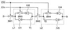
従来より、入力された信号を、時間を遅延させて出力するDフリップフロップ(以下DFFと記す)回路が知られている(例えば、特許文献1参照)。図6は、従来知られているDFF回路の回路図である。図6に示されるように、DFF回路は、第1ラッチ回路L1および第2ラッチ回路L2と、第1スイッチSW1および第2スイッチSW2と、を備えて構成されている。これらは、例えばMOSトランジスタにて形成される。 2. Description of the Related Art Conventionally, a D flip-flop (hereinafter referred to as DFF) circuit that outputs an input signal with a time delay is known (see, for example, Patent Document 1). FIG. 6 is a circuit diagram of a conventionally known DFF circuit. As shown in FIG. 6, the DFF circuit includes a first latch circuit L1 and a second latch circuit L2, and a first switch SW1 and a second switch SW2. These are formed by, for example, MOS transistors.
第1ラッチ回路L1は、入力する信号を一時的に保持する回路であり、第1および第2インバータIV1、IV2と、第3スイッチSW3と、を備えている。第2ラッチ回路L2は、第1ラッチ回路L1と同じ働きをするものであり、第3および第4インバータIV3、IV4と、第4スイッチSW4と、を備えている。 The first latch circuit L1 is a circuit that temporarily holds a signal to be input, and includes first and second inverters IV1 and IV2 and a third switch SW3. The second latch circuit L2 has the same function as the first latch circuit L1, and includes third and fourth inverters IV3 and IV4 and a fourth switch SW4.
第1スイッチSW1は、外部回路からのデータ信号を第1ラッチ回路L1に入力するものである。また、第2スイッチSW2は、第1および第2ラッチ回路L1、L2を接続するものである。なお、上記第1〜第4スイッチSW1〜SW4は、クロックパルスのハイレベルが入力されると接続、クロックパルスのローレベルが入力されると開放されるようになっている。 The first switch SW1 inputs a data signal from an external circuit to the first latch circuit L1. The second switch SW2 connects the first and second latch circuits L1 and L2. The first to fourth switches SW1 to SW4 are connected when a high level of the clock pulse is input, and are opened when a low level of the clock pulse is input.
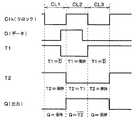
このようなDFF回路の作動を、図7を参照して説明する。図7は、図6に示されるDFF回路のタイムチャートである。このタイムチャートは、図6に示されるDFF回路図において、クロックパルスのハイレベルまたはローレベルに応じた第1ラッチ回路L1の電位T1、第2ラッチ回路L2の電位T2、および出力信号Qの各パルスを示している。 The operation of such a DFF circuit will be described with reference to FIG. FIG. 7 is a time chart of the DFF circuit shown in FIG. This time chart shows the potential T1 of the first latch circuit L1, the potential T2 of the second latch circuit L2, and the output signal Q according to the high level or low level of the clock pulse in the DFF circuit diagram shown in FIG. Shows a pulse.
DFF回路にクロックパルスのローレベルが入力される(図7の区間CL1)と、第1スイッチSW1および第2ラッチ回路L2の第4スイッチSW4が接続される。DFF回路にクロックパルスのローレベルが入力されている期間にデータ信号DがDFF回路に入力されると、そのデータ信号Dは、第1ラッチ回路L1にラッチされる。これにより、電位T1はT1=−Dとなる。 When the low level of the clock pulse is input to the DFF circuit (section CL1 in FIG. 7), the first switch SW1 and the fourth switch SW4 of the second latch circuit L2 are connected. When the data signal D is input to the DFF circuit during the period when the low level of the clock pulse is input to the DFF circuit, the data signal D is latched by the first latch circuit L1. As a result, the potential T1 becomes T1 = −D.
さらに、DFF回路にクロックパルスのローレベルが入力される場合、第2スイッチSW2および第1ラッチ回路L1の第3スイッチSW3が開放される。これにより、第1ラッチ回路L1と第2ラッチ回路L2とは電気的に切断された状態になる。また、第4スイッチSW4が接続されるため、第2ラッチ回路L2がループ回路となる。これにより、出力信号Q=―T2として外部回路に出力され続ける。 Further, when the low level of the clock pulse is input to the DFF circuit, the second switch SW2 and the third switch SW3 of the first latch circuit L1 are opened. As a result, the first latch circuit L1 and the second latch circuit L2 are electrically disconnected. Further, since the fourth switch SW4 is connected, the second latch circuit L2 becomes a loop circuit. As a result, the output signal Q = −T2 continues to be output to the external circuit.
一方、DFF回路にクロックパルスのハイレベルが入力される(図7の区間CL2)と、第2スイッチSW2および第1ラッチ回路L1の第3スイッチSW3が接続される。これにより、T2=T1(=―D)となり、第1ラッチ回路L1にラッチされていたデータ信号Dが第2ラッチ回路L2に移る。そして、出力信号Q=―T2(=―T1=D)として出力される。 On the other hand, when the high level of the clock pulse is input to the DFF circuit (section CL2 in FIG. 7), the second switch SW2 and the third switch SW3 of the first latch circuit L1 are connected. As a result, T2 = T1 (= −D), and the data signal D latched in the first latch circuit L1 moves to the second latch circuit L2. An output signal Q = −T2 (= −T1 = D) is output.
再び、DFF回路にクロックパルスのローレベルが入力される(図7の区間CL3)と、
第1および第4スイッチSW1、SW4が開放される。これにより、外部回路からの入力が遮断されると共に、出力信号Qが出力され続ける。
The first and fourth switches SW1 and SW4 are opened. As a result, the input from the external circuit is cut off and the output signal Q is continuously output.
上記のようなDFF回路を、車両に搭載するセンサ、例えば車輪速度センサに採用すると、以下の問題が生じることが発明者らの検討により明らかとなった。例えば車輪速度センサなどのセンサは、そのセンサを制御するECUから長い配線を介して車両の所定場所に設置される。つまり、配線のノイズや振動により、センサに供給される電源が変動しやすい状態となる。 When the DFF circuit as described above is employed in a sensor mounted on a vehicle, for example, a wheel speed sensor, the inventors have found that the following problems occur. For example, a sensor such as a wheel speed sensor is installed at a predetermined location of the vehicle through a long wiring from an ECU that controls the sensor. In other words, the power supplied to the sensor is likely to fluctuate due to wiring noise and vibration.
ところが、上記従来の技術では、DFF回路に供給される電源が一瞬でも途絶えると、第1ラッチ回路L1または第2ラッチ回路L2にて保持していたデータ信号が消えてしまうという問題が生じる。すなわち、電源が供給されなくなることでMOSトランジスタ自体は作動しなくなり、データ信号は保持され続けると考えられるが、MOSトランジスタでDFF回路を構成しているため、いわゆるPN接合が存在すると共に、この接合部位にて微少なリーク電流が流れることでラッチ回路の保持状態が解除されてしまう。 However, in the conventional technique, when the power supplied to the DFF circuit is interrupted even for a moment, the data signal held in the first latch circuit L1 or the second latch circuit L2 is lost. That is, it is considered that the MOS transistor itself does not operate when the power is not supplied and the data signal continues to be held. However, since the MOS transistor constitutes a DFF circuit, a so-called PN junction exists, and this junction When a minute leak current flows at the part, the holding state of the latch circuit is released.
本発明は、上記点に鑑み、供給される電源の一時的な低下もしくは停止に対してデータを保持し続けることができる電源瞬断対応論理回路を提供することを目的とする。 The present invention has been made in view of the above points, and it is an object of the present invention to provide an instantaneous power failure response logic circuit capable of continuing to hold data against a temporary drop or stop of the supplied power.
上記目的を達成するため、請求項1に記載の発明では、入力されるデータ信号を一時的に保持すると共に、クロックパルスが入力される任意のタイミングでデータ信号を出力するフリップフロップ回路として構成される電源瞬断対応論理回路であって、データ信号に対応した電圧を保持するコンデンサ(CP1〜CP5)と、コンデンサに保持されている電圧の変動を抑制する抵抗(RS1〜RS5、IV5、IV6)と、を備え、フリップフロップ回路に対する電源供給が一時的に低下または停止した時、抵抗およびコンデンサにて形成されるRC回路の時定数によって決まる時間、コンデンサに保持される電圧がフリップフロップ回路に保持されるデータ信号とされることを特徴としている。 In order to achieve the above object, the invention according to
このように、データ信号を保持するコンデンサと、コンデンサにて保持されている電圧の変動を抑制する抵抗と、を電源瞬断対応回路内に設ける。これにより、電源瞬断対応論理回路に対して電源供給が一時的に低下もしくは停止したとしても、コンデンサによって電源瞬断対応論理回路内にラッチされたデータ信号に対応した電圧を保持することができる。 As described above, the capacitor that holds the data signal and the resistor that suppresses the fluctuation of the voltage held by the capacitor are provided in the power supply interruption correspondence circuit. As a result, even if the power supply is temporarily reduced or stopped for the power supply interruption-response logic circuit, the voltage corresponding to the data signal latched in the power supply interruption-response logic circuit by the capacitor can be held. .
さらに、コンデンサと共に電源瞬断対応論理回路内に設けられた抵抗によって、電源瞬断対応論理回路に対して電源供給が一時的に低下もしくは停止した時や、電源供給の復帰中における電源瞬断対応論理回路の不安定な動作状態によって、コンデンサに保持されていたデータ信号の電圧が変動してしまうことを防止することができる。 In addition, the power supply for the instantaneous power failure response logic circuit is temporarily reduced or stopped by the resistor provided in the logic circuit for the instantaneous power failure response together with the capacitor, or the power supply is responded to when the power supply is restored. It is possible to prevent the voltage of the data signal held in the capacitor from fluctuating due to an unstable operation state of the logic circuit.
請求項2に記載の発明では、第1スイッチ(SW1)を介して外部回路からデータ信号が入力されると共に、データ信号をラッチする第1ラッチ回路(L1)と、第2スイッチ(SW2)を介して第1ラッチ回路にてラッチされているデータ信号を入力し、そのデータ信号をラッチすると共に外部回路に出力する第2ラッチ回路(L2)と、を備え、第1、第2ラッチ回路は、データ信号に対応した電圧を保持する第1、第2コンデンサ(CP1、CP2)と、第1、第2コンデンサにて保持される電圧の変動を抑制する第1、第2抵抗(RS1、RS2)と、をそれぞれ有し、第1、第2ラッチ回路に対する電源供給が一時的に低下または停止した時、第1、第2コンデンサおよび第1、第2抵抗にてそれぞれ形成されるRC回路の時定数によって決まる時間、第1、第2コンデンサにそれぞれ保持される電圧が第1、第2ラッチ回路にそれぞれ保持されるデータ信号とされることを特徴としている。 According to the second aspect of the present invention, the data signal is input from the external circuit through the first switch (SW1), and the first latch circuit (L1) for latching the data signal and the second switch (SW2) are provided. And a second latch circuit (L2) for inputting the data signal latched by the first latch circuit and latching the data signal and outputting to the external circuit. The first and second latch circuits are The first and second capacitors (CP1, CP2) that hold the voltage corresponding to the data signal, and the first and second resistors (RS1, RS2) that suppress fluctuations in the voltage held by the first and second capacitors And when the power supply to the first and second latch circuits is temporarily lowered or stopped, the RC circuit formed by the first and second capacitors and the first and second resistors respectively. Time constant Thus determined time, the voltage held in the first, second capacitor is characterized by being the first, each of the data signal held in the second latch circuit.
このように、データ信号を保持する第1、第2ラッチ回路に、データ信号に対応した電圧を保持する第1、第2コンデンサを設ける。これにより、電源瞬断対応論理回路に対して電源供給が一時的に低下もしくは停止した場合、各ラッチ回路にラッチされているデータ信号を保持し続けることができる。また、第1、第2コンデンサにて保持される電圧の変動を抑制する抵抗も設ける。これにより、電源供給の一次停止時や復旧時に第1、第2コンデンサに保持されている電圧が変動してしまうことを防止することができる。 In this way, the first and second capacitors that hold the voltage corresponding to the data signal are provided in the first and second latch circuits that hold the data signal. As a result, when the power supply is temporarily lowered or stopped with respect to the instantaneous power interruption logic circuit, the data signal latched in each latch circuit can be held. Also, a resistor that suppresses fluctuations in the voltage held by the first and second capacitors is provided. As a result, it is possible to prevent the voltage held in the first and second capacitors from fluctuating when the power supply is temporarily stopped or restored.
請求項3に記載の発明では、第1、第2コンデンサは、その電極の一方が第1、第2抵抗の電流出力側に接続されていることを特徴としている。 The invention according to claim 3 is characterized in that one of the electrodes of the first and second capacitors is connected to the current output side of the first and second resistors.
このように、第1、第2コンデンサを第1、第2抵抗の電流出力側に接続する。これにより、電源供給の一次停止時や復旧時に第1、第2ラッチ回路内にて起こる電流の逆流(いわゆる電流の吸い込み)に対して、第1、第2コンデンサに保持されていた電圧が消失されないようにすることができる。 In this way, the first and second capacitors are connected to the current output side of the first and second resistors. As a result, the voltage held in the first and second capacitors disappears against the reverse current (so-called current sink) that occurs in the first and second latch circuits when the power supply is temporarily stopped or restored. Can be prevented.
請求項4に記載の発明では、第1、第2ラッチ回路において、第1、第2コンデンサおよび第1、第2抵抗によってそれぞれ決まる時定数は、第1、第2ラッチ回路に対する電源供給が一時的に低下または停止している時間よりも長くなるように、第1、第2コンデンサおよび第1、第2抵抗の値がそれぞれ設定されるようになっていることを特徴としている。 According to a fourth aspect of the present invention, in the first and second latch circuits, the time constants determined by the first and second capacitors and the first and second resistors, respectively, are temporarily supplied with power to the first and second latch circuits. The values of the first and second capacitors and the first and second resistors are set so as to be longer than the time during which they are lowered or stopped.
このように、第1、第2コンデンサおよび第1、第2抵抗でそれぞれ決まる時定数を、第1、第2ラッチ回路に対する電源供給が一時的に低下または停止している時間よりも長くなるように設定する。これにより、データ信号を時定数時間保持することができ、電源供給が一時的に低下または停止している期間、データ信号を保持し続けることができる。したがって、データ信号を消失させないようにすることができる。 As described above, the time constants determined by the first and second capacitors and the first and second resistors are set to be longer than the time during which the power supply to the first and second latch circuits is temporarily lowered or stopped. Set to. As a result, the data signal can be held for a time constant time, and the data signal can be held for a period during which the power supply is temporarily lowered or stopped. Therefore, it is possible to prevent the data signal from being lost.
なお、上記各手段の括弧内の符号は、後述する実施形態に記載の具体的手段との対応関係を示すものである。 In addition, the code | symbol in the bracket | parenthesis of each said means shows the correspondence with the specific means as described in embodiment mentioned later.
(第1実施形態)
以下、本発明の第1実施形態について図を参照して説明する。以下では、図6に示す構成要素と同一のものには、同一符号を記してある。(First embodiment)
Hereinafter, a first embodiment of the present invention will be described with reference to the drawings. In the following, the same components as those shown in FIG.
図1は、本発明の一実施形態に係る電源瞬断対応論理回路の回路図である。図1に示されるように、電源瞬断対応論理回路は、入力されたデータ信号を一時的に保持すると共にそのデータ信号を任意のタイミングで出力する、いわゆるD−フリップフロップ回路であって、第1スイッチSW1と、第1ラッチ回路L1と、第2スイッチSW2と、第2ラッチ回路L2と、を備えて構成されている。 FIG. 1 is a circuit diagram of a logic circuit for power interruption according to an embodiment of the present invention. As shown in FIG. 1, the instantaneous power failure logic circuit is a so-called D-flip-flop circuit that temporarily holds an input data signal and outputs the data signal at an arbitrary timing. The first switch SW1, the first latch circuit L1, the second switch SW2, and the second latch circuit L2 are provided.
第1スイッチSW1は、入力されるクロックパルスのハイレベルまたはローレベルに応じて第1スイッチSW1の一端側と他端側とを接続(導通)または開放(断線)するものである。この第1スイッチSW1は、例えば半導体基板にMOSトランジスタとして形成される。 The first switch SW1 connects (conducts) or opens (disconnects) one end side and the other end side of the first switch SW1 according to the high level or low level of the input clock pulse. The first switch SW1 is formed as a MOS transistor on a semiconductor substrate, for example.
第1ラッチ回路L1は、入力される信号を一時的に保持するものであり、第1インバータIV1と、第2インバータIV2と、第3スイッチSW3と、第1コンデンサCP1と、第1抵抗RS1と、を備えて構成されている。 The first latch circuit L1 temporarily holds an input signal, and includes a first inverter IV1, a second inverter IV2, a third switch SW3, a first capacitor CP1, and a first resistor RS1. , And is configured.
第1および第2インバータIV1、IV2は、入力されたデジタル信号を反転して出力するものである。また、第3スイッチSW3は、第1スイッチSW1と同様のものである。これら、第1および第2インバータIV1、IV2および第3スイッチSW3は、例えば半導体基板にMOSトランジスタとして形成される。 The first and second inverters IV1 and IV2 invert the input digital signal and output it. The third switch SW3 is the same as the first switch SW1. The first and second inverters IV1, IV2 and the third switch SW3 are formed as MOS transistors on a semiconductor substrate, for example.
第1コンデンサCP1は、電源瞬断対応論理回路に供給される電源が一時的に低下もしくは停止する場合、第1ラッチ回路L1にラッチされているデータ信号を保持し続けるためのものである。図1に示されるように、第1コンデンサCP1の一方の電極が、第2インバータIV2と第1抵抗RS1との間に接続され、他方の電極が接地された状態とされる。この第1コンデンサCP1は、その電極の一方が後述する第1抵抗RS1の電流出力側に接続されている。 The first capacitor CP1 is for continuing to hold the data signal latched in the first latch circuit L1 when the power supplied to the instantaneous power interruption logic circuit is temporarily lowered or stopped. As shown in FIG. 1, one electrode of the first capacitor CP1 is connected between the second inverter IV2 and the first resistor RS1, and the other electrode is grounded. The first capacitor CP1 has one of its electrodes connected to a current output side of a first resistor RS1 described later.
本実施形態では、第1コンデンサCP1として20pFの容量のものが採用される。なお、ここでは第1コンデンサCP1の容量を20pFとしているが、5〜50pFの範囲、より好ましくは20pFである。 In the present embodiment, a capacitor having a capacity of 20 pF is employed as the first capacitor CP1. In addition, although the capacity | capacitance of 1st capacitor | condenser CP1 is 20 pF here, it is the range of 5-50 pF, More preferably, it is 20 pF.
第1抵抗RS1は、電源瞬断対応論理回路に供給される電源が一時的に低下もしくは停止した時、または、再び電源が供給される復旧時、第1コンデンサCP1にて保持されている電圧の変動を抑制するものである。詳しくは、第1コンデンサCP1に蓄積された電荷が第1インバータIV1側に流れることを防止するものである。つまり、第1抵抗RS1は、第1インバータIV1の電流吸い込みに耐えられる抵抗値を有するものが採用される。このような第1抵抗RS1は、例えばNi等の金属、Poly―SiやSiCr等で形成される薄膜抵抗(もしくは非拡散抵抗)で構成され、0.5MΩのものが採用される。なお、ここでは第1抵抗RS1の抵抗を0.5MΩとしているが、0.2〜2MΩの範囲、より好ましくは0.5MΩである。 The first resistor RS1 has a voltage held by the first capacitor CP1 when the power supplied to the instantaneous power interruption logic circuit is temporarily reduced or stopped, or when power is supplied again. It suppresses fluctuations. Specifically, the charge accumulated in the first capacitor CP1 is prevented from flowing to the first inverter IV1 side. That is, the first resistor RS1 has a resistance value that can withstand the current sink of the first inverter IV1. The first resistor RS1 is composed of a thin film resistor (or non-diffused resistor) formed of, for example, a metal such as Ni, Poly-Si, SiCr, or the like, and a 0.5 MΩ resistor is employed. In addition, although resistance of 1st resistance RS1 is 0.5 M (ohm) here, it is the range of 0.2-2 M (ohm), More preferably, it is 0.5 M (ohm).
この第1抵抗RS1は、第1インバータIV1と第2インバータIV2との間に接続され、その一端側が第1インバータIV1側に接続され、他端側が第1コンデンサCP1の電極および第2インバータIV2側に接続されている。このような第1抵抗RS1の配置により、電源の一時的な低下もしくは停止によって第1インバータIV1側に電流が流れてしまうことを防止し、第1コンデンサCP1に保持されているデータ信号を消失させないようにしている。 The first resistor RS1 is connected between the first inverter IV1 and the second inverter IV2, one end side thereof is connected to the first inverter IV1 side, and the other end side thereof is connected to the electrode of the first capacitor CP1 and the second inverter IV2 side. It is connected to the. Such an arrangement of the first resistor RS1 prevents a current from flowing to the first inverter IV1 side due to a temporary drop or stop of the power supply, and does not erase the data signal held in the first capacitor CP1. I am doing so.
第2スイッチSW2は、第1スイッチSW1と同様に、入力されるクロックパルスに応じて第2スイッチSW2の一端側(第1ラッチ回路L1側)と他端側(第2ラッチ回路L2側)とを接続または開放するものである。 Similarly to the first switch SW1, the second switch SW2 has one end side (first latch circuit L1 side) and the other end side (second latch circuit L2 side) of the second switch SW2 according to the input clock pulse. Is connected or released.
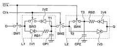
第2ラッチ回路L2は、第1ラッチ回路L1と同様に、入力される信号を一時的に保持するものである。第2ラッチ回路L2の構成は、第1ラッチ回路L1と同様であり、第1ラッチ回路L1の第1インバータIV1、第2インバータIV2、第3スイッチSW3、第1コンデンサCP1、第1抵抗RS1がそれぞれ第2ラッチ回路L2の第3インバータIV3、第4インバータIV4、第4スイッチSW4、第2コンデンサCP2、第2抵抗RS2に対応し、それぞれが第1ラッチ回路L1と同様の機能を果たす。 Similar to the first latch circuit L1, the second latch circuit L2 temporarily holds an input signal. The configuration of the second latch circuit L2 is the same as that of the first latch circuit L1, and the first inverter IV1, the second inverter IV2, the third switch SW3, the first capacitor CP1, and the first resistor RS1 of the first latch circuit L1 are included. Each corresponds to the third inverter IV3, the fourth inverter IV4, the fourth switch SW4, the second capacitor CP2, and the second resistor RS2 of the second latch circuit L2, and each performs the same function as the first latch circuit L1.
なお、第2ラッチ回路L2において、第2抵抗RS2は第4インバータIV4と第4スイッチSW4との間に接続されている。また、第2コンデンサCP2の一方の電極は、第2抵抗RS2と第4スイッチSW4との間に接続されている。 In the second latch circuit L2, the second resistor RS2 is connected between the fourth inverter IV4 and the fourth switch SW4. One electrode of the second capacitor CP2 is connected between the second resistor RS2 and the fourth switch SW4.
以上が、電源瞬断対応論理回路の構成である。上記構成は、例えば1チップ内に作り込まれるようになっており、各構成要素は図示しない電源線から電源が供給されることで作動するようになっている。また、本実施形態では、第1〜第4スイッチSW1〜SW4は、クロックパルスのハイレベルが入力されると接続、ローレベルが入力されると開放されるようになっている。 The above is the configuration of the power supply interruption logic circuit. The above-mentioned configuration is built in, for example, one chip, and each component operates by being supplied with power from a power line (not shown). In the present embodiment, the first to fourth switches SW1 to SW4 are connected when a high level of the clock pulse is input, and are opened when a low level is input.
また、限定するものではないが、本発明に係る電源瞬断対応論理回路は、車両に搭載されるセンサ、例えば逆回転も検出できる車輪速度センサ、加速度センサ、ヨーレートセンサ等に採用される。 Although not limited thereto, the power supply interruption-response logic circuit according to the present invention is employed in a sensor mounted on a vehicle, for example, a wheel speed sensor that can detect reverse rotation, an acceleration sensor, a yaw rate sensor, and the like.
次に、第1および第2抵抗RS1、RS2の値、第1および第2コンデンサCP1、CP2の値の設定方法について説明する。まず、上記第1および第2ラッチ回路L1、L2では、第1および第2抵抗RS1、RS2と第1および第2コンデンサCP1、CP2によってRC回路が構成され、これらの値に応じて第1および第2コンデンサCP1、CP2の充放電時間、すなわち時定数(=RC)が決まる。したがって、電源瞬断時に各ラッチ回路L1、L2にてデータ信号を保持し続けるためには、少なくとも、この時定数の値が、電源が一時的に低下する時間(例えば1〜2μs)よりも長くなければならない。 Next, a method for setting the values of the first and second resistors RS1 and RS2 and the values of the first and second capacitors CP1 and CP2 will be described. First, in the first and second latch circuits L1 and L2, an RC circuit is configured by the first and second resistors RS1 and RS2 and the first and second capacitors CP1 and CP2. The charging / discharging time of the second capacitors CP1 and CP2, that is, the time constant (= RC) is determined. Therefore, in order to keep holding the data signal in each of the latch circuits L1 and L2 when the power supply is instantaneously interrupted, at least the value of this time constant is longer than the time during which the power supply temporarily decreases (for example, 1 to 2 μs). There must be.
一般に、抵抗およびコンデンサの充放電時間波形が、ロジック回路の誤作動を引き起こす電圧値(≒電源電圧/2)に達する時間は、0.7×時定数である。このことから、電源が一時的に低下する時間の1.44倍以上の抵抗の値およびコンデンサの容量を設定する必要がある。しかしながら、各抵抗RS1、RS2および各コンデンサCP1、CP2の値を大きくし過ぎると、回路の要求される最大動作周波数(例えば100μs)に、この電源瞬断対応論理回路が対応できなくなる。 In general, the time required for the charge and discharge time waveforms of the resistor and the capacitor to reach a voltage value (≈power supply voltage / 2) that causes malfunction of the logic circuit is 0.7 × time constant. For this reason, it is necessary to set a resistance value and a capacitance of the capacitor that are 1.44 times or more as long as the power supply temporarily decreases. However, if the values of the resistors RS1 and RS2 and the capacitors CP1 and CP2 are too large, the instantaneous power failure logic circuit cannot cope with the maximum operating frequency required for the circuit (for example, 100 μs).
そこで、各コンデンサCP1、CP2への充放電電圧を電源電圧比でほぼ飽和していると考えられる0.9以上、もしくは0.1以下にするためには、最小クロック時間(=1/最大クロック周波数)>2.3×RCとなる。実際の作動においては、最大動作周波数の3分の1程度の時間とすることで電源の一時的低下に十分に対応できる。よって、本実施形態で対応できる時間は(1/3)×最小クロック時間(RC=(1/2.3)×最小クロック時間)となる。 Therefore, in order to set the charge / discharge voltage to each of the capacitors CP1 and CP2 to 0.9 or more, or 0.1 or less, which is considered to be almost saturated at the power supply voltage ratio, the minimum clock time (= 1 / maximum clock) Frequency)> 2.3 × RC. In actual operation, it is possible to sufficiently cope with a temporary decrease in power by setting the time to about one third of the maximum operating frequency. Therefore, the time that can be handled in this embodiment is (1/3) × minimum clock time (RC = (1 / 2.3) × minimum clock time).
上記のように、最大動作周波数を例えば100μsとすると、時定数をその3分の1である10〜30μs程度とすれば良い。この時間であれば、電源の一時的低下時間が例えば数μsであるので、十分に対応できる。 As described above, if the maximum operating frequency is set to 100 μs, for example, the time constant may be set to about 10 to 30 μs that is one third of the time constant. If it is this time, since the power supply temporary fall time is several microseconds, for example, it can respond sufficiently.
本実施形態では、時定数を10μsとし、この時定数となるような各抵抗RS1、RS2および各コンデンサCP1、CP2を設定する。具体的には、例えば半導体基板上に電源瞬断対応論理回路を設計する際、各抵抗RS1、RS2および各コンデンサCP1、CP2をパターン面積のバランスを考慮して設定する。時定数を10μsとすると、抵抗の値を大きくした場合、2MΩ×5pFとすることができる。一方、コンデンサの値を大きくした場合、0.2MΩ×50pFとすることができる。本実施形態では、0.5MΩ×20pFとしている。 In the present embodiment, the time constant is set to 10 μs, and the resistors RS1 and RS2 and the capacitors CP1 and CP2 are set so as to be the time constant. Specifically, for example, when designing a logic circuit for instantaneous power interruption on a semiconductor substrate, the resistors RS1 and RS2 and the capacitors CP1 and CP2 are set in consideration of a balance of pattern areas. If the time constant is 10 μs, 2 MΩ × 5 pF can be obtained when the resistance value is increased. On the other hand, when the value of the capacitor is increased, it can be 0.2 MΩ × 50 pF. In this embodiment, it is set to 0.5 MΩ × 20 pF.
上記のように、各抵抗RS1、RS2および各コンデンサCP1、CP2を設定し、電源瞬断対応論理回路に対する電源供給が一時的に低下もしくは停止した場合(1〜2μs)、各ラッチ回路L1、L2にラッチされていたデータ信号は、各コンデンサCP1、CP2によって時定数の時間(10μs)保持される。そして、電源供給が一時的に低下もしくは停止している時、もしくは電源の復旧時において、各抵抗RS1、RS2の存在により、第1および第2コンデンサCP1、CP2に蓄積された電荷が第1および第4インバータIV1、IV4側に吸い込まれないようにして、データ信号が失われないようにする。 As described above, when the resistors RS1 and RS2 and the capacitors CP1 and CP2 are set, and the power supply to the instantaneous power failure corresponding logic circuit is temporarily lowered or stopped (1 to 2 μs), the latch circuits L1 and L2 The data signal latched in (1) is held for a time constant time (10 μs) by the capacitors CP1 and CP2. Then, when the power supply is temporarily lowered or stopped, or when the power supply is restored, the electric charges accumulated in the first and second capacitors CP1 and CP2 are caused by the presence of the resistors RS1 and RS2. The data signal is not lost by preventing it from being sucked into the fourth inverters IV1 and IV4.
このようにして、電源瞬断対応論理回路に対する電源供給が一時的に低下もしくは停止した場合であっても、第1および第2抵抗RS1、RS2および第1および第2コンデンサCP1、CP2にてそれぞれ形成されるRC回路の時定数によって決まる時間、第1および第2コンデンサCP1、CP2にそれぞれ保持される電圧が第1および第2ラッチ回路L1、L2に保持されるデータ信号とされる。 In this manner, even when the power supply to the power supply circuit for instantaneous power interruption is temporarily lowered or stopped, the first and second resistors RS1 and RS2 and the first and second capacitors CP1 and CP2 respectively. The voltage held in the first and second capacitors CP1 and CP2 for the time determined by the time constant of the formed RC circuit is used as the data signal held in the first and second latch circuits L1 and L2.
続いて、図1に示される電源瞬断対応論理回路の回路作動について、図2に示されるタームチャートを参照して説明する。図2においては、クロック(Clk)、D(データ信号)、図1に示される回路図の電位T1、電位T2、電位T3、そしてQ(出力信号)の各パルスが示されている。ここで、電位T1は第1ラッチ回路L1にラッチされるデータ信号である。電位T2は電位T1と同電位であり、第2ラッチ回路L2にラッチされるデータ信号である。電位T3は電位T2と同電位であり、第2コンデンサCP2の電位である。 Next, the circuit operation of the power supply interruption logic circuit shown in FIG. 1 will be described with reference to the term chart shown in FIG. In FIG. 2, pulses of clock (Clk), D (data signal), potential T1, potential T2, potential T3, and Q (output signal) in the circuit diagram shown in FIG. 1 are shown. Here, the potential T1 is a data signal latched by the first latch circuit L1. The potential T2 is the same potential as the potential T1, and is a data signal latched by the second latch circuit L2. The potential T3 is the same potential as the potential T2, and is the potential of the second capacitor CP2.
なお、説明をわかりやすくするため、データ信号Dが第1ラッチ回路L1に入力される以前に、第1および第2ラッチ回路L1、L2にはデータ信号Dがラッチされていないものとする。 For ease of explanation, it is assumed that the data signal D is not latched in the first and second latch circuits L1 and L2 before the data signal D is input to the first latch circuit L1.
まず、電源瞬断対応論理回路にクロックパルスのローレベルが入力される(区間CL1)と、第1および第4スイッチSW1、SW4が接続、第2および第3スイッチSW2、SW3が開放される。この状態で、外部回路から電源瞬断対応論理回路にデータ信号Dのハイレベルが入力されると、第1ラッチ回路L1において、電位T1は第1インバータIV1によってデータ信号Dが反転した信号(T1=−D)となる。ここで、図2の区間CL1に示されるように、データ信号の立ち上がりに対して、電位T1は時定数の時間、すなわち本実施形態では10μs遅れて立ち下がる。 First, when a low level of the clock pulse is input to the instantaneous power interruption logic circuit (section CL1), the first and fourth switches SW1 and SW4 are connected, and the second and third switches SW2 and SW3 are opened. In this state, when the high level of the data signal D is input from the external circuit to the power supply interruption-response logic circuit, in the first latch circuit L1, the potential T1 is the signal (T1 = −D). Here, as shown in a section CL1 in FIG. 2, the potential T1 falls with a time of time constant, that is, with a delay of 10 μs in this embodiment, with respect to the rise of the data signal.
一方、第2ラッチ回路L2においては、第1ラッチ回路L1と電気的に切断された状態になっているとともに、ループ回路が形成される。第2ラッチ回路L2にはデータ信号Dが保持されていないため、電位T2は図2に示されるようにハイレベルになっている。また、電位T3は電位T2と同電位であるため、ハイレベルになっている。なお、第2ラッチ回路L2にはデータ信号Dが保持されていないため、出力信号Q(=―T2=―T3)はローレベルになっている。 On the other hand, the second latch circuit L2 is electrically disconnected from the first latch circuit L1, and a loop circuit is formed. Since the data signal D is not held in the second latch circuit L2, the potential T2 is at a high level as shown in FIG. Further, since the potential T3 is the same potential as the potential T2, it is at a high level. Since the data signal D is not held in the second latch circuit L2, the output signal Q (= −T2 = −T3) is at a low level.
次に、電源瞬断対応論理回路にクロックパルスのハイレベルが入力される(区間CL2)と、第1および第4スイッチSW1、SW4が開放、第2および第3スイッチSW2、SW3が接続される。第1ラッチ回路L1においては、ループ回路が形成され、区間CL1に第1ラッチ回路L1に入力されたデータ信号Dがラッチされる。したがって、図2の区間CL2に示されるように、電位T1はローレベルが保持される。 Next, when a high level of the clock pulse is input to the instantaneous power interruption logic circuit (section CL2), the first and fourth switches SW1 and SW4 are opened, and the second and third switches SW2 and SW3 are connected. . In the first latch circuit L1, a loop circuit is formed, and the data signal D input to the first latch circuit L1 is latched in the interval CL1. Therefore, as shown in the interval CL2 in FIG. 2, the potential T1 is kept at a low level.
第2ラッチ回路L2においては、第2スイッチSW2が接続されているので、電位T2は第1ラッチ回路L1に保持されているデータ信号Dと同電位、すなわち電位T1と同電位になる。同様に、電位T3は電位T2と同電位になる。このとき、電位T3は、RC回路によって時定数の時間だけ遅れて電位T2と同電位になる。そして、出力信号Qは、第3および第4インバータIV3、IV4の存在により、電位T2および電位T3の反転信号(Q=―T3=−T2=−T1=D)として出力される。 In the second latch circuit L2, since the second switch SW2 is connected, the potential T2 becomes the same potential as the data signal D held in the first latch circuit L1, that is, the same potential as the potential T1. Similarly, the potential T3 is the same as the potential T2. At this time, the potential T3 becomes the same potential as the potential T2 with a delay of the time constant by the RC circuit. The output signal Q is output as the potential T2 and the inverted signal of the potential T3 (Q = −T3 = −T2 = −T1 = D) due to the presence of the third and fourth inverters IV3 and IV4.
再び、電源瞬断対応論理回路にクロックパルスのローレベルが入力される(区間CL3)と、上記と同様にしてデータ信号のラッチおよび出力がなされる。 When the low level of the clock pulse is input again to the instantaneous power interruption logic circuit (section CL3), the data signal is latched and output in the same manner as described above.
図2の電位T1、電位T3のパルス波形に示されるように、各ラッチ回路L1、L2に保持されるデータ信号Dは、時定数の時間だけ遅れて保持される。つまり、この時定数の時間の遅れによって、電源瞬断対応論理回路に対する電源供給の一時的な低下もしくは停止した場合であっても、第1および第2ラッチ回路L1、L2にてデータ信号Dを保持し続けることができるのである。 As shown in the pulse waveforms of the potential T1 and the potential T3 in FIG. 2, the data signal D held in each of the latch circuits L1 and L2 is held with a time constant delay. That is, even when the power supply to the instantaneous power interruption corresponding logic circuit is temporarily lowered or stopped due to the time constant delay, the first and second latch circuits L1 and L2 send the data signal D. You can keep it.
以上説明したように、本実施形態では、第1および第2ラッチ回路L1、L2において、データ信号を保持する第1および第2コンデンサCP1、CP2と、第1および第2コンデンサCP1、CP2にて保持されている電圧の変動を抑制する第1および第2抵抗RS1、RS2と、をそれぞれ設ける。これにより、電源瞬断対応論理回路に対して電源供給が一時的に低下もしくは停止したとしても、第1および第2コンデンサCP1、CP2によって電源瞬断対応論理回路内にラッチされたデータ信号に対応した電圧を保持することができる。 As described above, in the present embodiment, in the first and second latch circuits L1 and L2, the first and second capacitors CP1 and CP2 holding the data signal and the first and second capacitors CP1 and CP2 are used. First and second resistors RS1 and RS2 that suppress fluctuations in the held voltage are provided. As a result, even if the power supply is temporarily lowered or stopped for the power supply interruption-response logic circuit, it corresponds to the data signal latched in the power supply interruption-response logic circuit by the first and second capacitors CP1 and CP2. Voltage can be maintained.
また、第1および第2コンデンサCP1、CP2と共に電源瞬断対応論理回路内に設けられた第1および第2抵抗RS1、RS2によって、電源供給の一時的低下および停止や、電源供給の復帰中などにおける電源瞬断対応論理回路の不安定な動作状態によって、第1および第2コンデンサCP1、CP2に保持されていたデータ信号の電圧が変動してしまうことを防止することができる。 In addition, the first and second resistors RS1 and RS2 provided in the logic circuit corresponding to the instantaneous power interruption together with the first and second capacitors CP1 and CP2 temporarily decrease and stop the power supply, and the power supply is being restored. It is possible to prevent the voltage of the data signal held in the first and second capacitors CP1 and CP2 from fluctuating due to the unstable operation state of the power supply circuit for instantaneous power interruption in FIG.
さらに、本実施形態では、第1および第2コンデンサCP1、CP2を第1および第2抵抗RS1、RS2の電流出力側に接続している。これにより、電源供給の一次停止時や復旧時に第1および第2ラッチ回路L1、L2内にて起こる電流の逆流(いわゆる電流の吸い込み)に対して、第1および第2コンデンサCP1、CP2に保持されていた電圧が消失されないようにすることができる。 Further, in the present embodiment, the first and second capacitors CP1 and CP2 are connected to the current output side of the first and second resistors RS1 and RS2. Thus, the first and second capacitors CP1 and CP2 hold the current backflow (so-called current sink) that occurs in the first and second latch circuits L1 and L2 when the power supply is temporarily stopped or restored. The voltage that has been applied can be prevented from being lost.
そして、第1および第2コンデンサCP1、CP2および第1および第2抵抗RS1、RS2でそれぞれ決まる時定数を、第1および第2ラッチ回路L1、L2に対する電源供給が一時的に低下または停止している時間よりも長くなるように設定する。これにより、データ信号を時定数時間保持することができ、電源供給が一時的に低下または停止している期間、データ信号を保持し続けることができる。 The time constants determined by the first and second capacitors CP1 and CP2 and the first and second resistors RS1 and RS2, respectively, are set so that the power supply to the first and second latch circuits L1 and L2 is temporarily reduced or stopped. Set to be longer than the current time. As a result, the data signal can be held for a time constant time, and the data signal can be held for a period during which the power supply is temporarily lowered or stopped.
(第2実施形態)
本実施形態では、第1実施形態と異なる部分についてのみ説明する。本実施形態では、第1および第2コンデンサCP1、CP2と、第1および第2抵抗RS1、RS2が各ラッチ回路L1、L2中に配置される場所が第1実施形態と異なる。(Second Embodiment)
In the present embodiment, only different parts from the first embodiment will be described. In this embodiment, the first and second capacitors CP1 and CP2 and the first and second resistors RS1 and RS2 are different from the first embodiment in the places where they are arranged in the respective latch circuits L1 and L2.
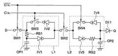
図3は、本実施形態に係る電源瞬断対応論理回路の回路図である。なお、第1実施形態と同じ構成要素には同じ符号を記してある。本実施形態では、第1実施形態に対して、第1ダイオードDI1が加えられた構成となっている。 FIG. 3 is a circuit diagram of the logic circuit for power interruption according to the present embodiment. In addition, the same code | symbol is described to the same component as 1st Embodiment. In the present embodiment, a first diode DI1 is added to the first embodiment.
図3に示されるように、第1ラッチ回路L1においては、第3スイッチSW3と第1インバータIV1との間に第1抵抗RS1が配置されている。さらに、第1コンデンサCP1の一方の電極が第1抵抗RS1と第1インバータIV1との間に接続されている。 As shown in FIG. 3, in the first latch circuit L1, the first resistor RS1 is disposed between the third switch SW3 and the first inverter IV1. Furthermore, one electrode of the first capacitor CP1 is connected between the first resistor RS1 and the first inverter IV1.
また、第2ラッチ回路L2においては、第3インバータIV3と第4インバータIV4との間に第2抵抗RS2が配置されている。さらに、第2コンデンサCP2の一方の電極が第2抵抗RS2と第4インバータIV4との間に接続されている。 In the second latch circuit L2, the second resistor RS2 is disposed between the third inverter IV3 and the fourth inverter IV4. Furthermore, one electrode of the second capacitor CP2 is connected between the second resistor RS2 and the fourth inverter IV4.
そして、第2ラッチ回路L2から出力されるデータ信号は、第1ダイオードDI1を通過して出力信号Qとして出力されるようになっている。この第1ダイオードDI1は、第第2抵抗RS2および第2コンデンサCP2によってアナログ信号とされたデータ信号を再びデジタル信号に変換する機能を有する。 The data signal output from the second latch circuit L2 passes through the first diode DI1 and is output as the output signal Q. The first diode DI1 has a function of converting a data signal converted into an analog signal by the second resistor RS2 and the second capacitor CP2 into a digital signal again.
このように、第1および第2ラッチ回路L1、L2において、第1および第2コンデンサCP1、CP2、第1および第2抵抗RS1、RS2の配置場所を変更することができる。本実施形態のように各コンデンサCP1、CP2および各抵抗RS1、RS2の設置場所を変更しても、上記第1実施形態と同様の効果が得られる。 As described above, in the first and second latch circuits L1 and L2, the arrangement locations of the first and second capacitors CP1 and CP2 and the first and second resistors RS1 and RS2 can be changed. Even if the installation locations of the capacitors CP1 and CP2 and the resistors RS1 and RS2 are changed as in the present embodiment, the same effects as in the first embodiment can be obtained.
(第3実施形態)
本実施形態では、第1および第2実施形態と異なる部分についてのみ説明する。本実施形態では、第1および第2抵抗RS1、RS2を無くしたことが第1および第2実施形態と異なる。(Third embodiment)
In the present embodiment, only parts different from the first and second embodiments will be described. In the present embodiment, the first and second resistors RS1 and RS2 are eliminated from the first and second embodiments.
図4−1は、本実施形態に係る電源瞬断対応論理回路の回路図である。図4−1に示されるように、本実施形態では、第1ラッチ回路L1は、第3スイッチSW3と、第2インバータIV2と、第1コンデンサCP1と、第5インバータIV5と、を備え構成される。また、第2ラッチ回路L2は、第4スイッチSW4と、第3インバータIV3と、第2コンデンサCP2と、第6インバータIV6と、を備え構成される。 FIG. 4A is a circuit diagram of the logic circuit for power interruption according to the present embodiment. As shown in FIG. 4A, in the present embodiment, the first latch circuit L1 includes a third switch SW3, a second inverter IV2, a first capacitor CP1, and a fifth inverter IV5. The The second latch circuit L2 includes a fourth switch SW4, a third inverter IV3, a second capacitor CP2, and a sixth inverter IV6.
これら第5および第6インバータIV5、IV6は、出力電流を制限する機能を有している。つまり、これら第5および第6インバータIV5、IV6は、抵抗が含まれた構成であると言える。 These fifth and sixth inverters IV5 and IV6 have a function of limiting the output current. That is, it can be said that the fifth and sixth inverters IV5 and IV6 have a configuration including a resistor.
具体的な回路例を図4−2に示す。図4−2は、図4−1に示される電源瞬断対応論理回路の等価回路図である。トランジスタTP1、TP2とトランジスタTN1、TN2はそれぞれゲートが共通に接続されており素子形状はゲート幅が10:1と異なっている。トランジスタTP1、TN1および抵抗R1により基準電流50uAが作られ、トランジスタTP1とトランジスタTP2(トランジスタTN1とトランジスタTN2も同様)とはカレントミラー動作をするため、素子サイズ比によりトランジスタTP2、TN2は5uAの電流しかソースもしくはシンク出来なくなる。トランジスタTP3、TN3は通常のインバータ用素子であり入力によりどちらかが導通する。 A specific circuit example is shown in FIG. FIG. 4-2 is an equivalent circuit diagram of the logic circuit for power supply interruption shown in FIG. 4-1. The gates of the transistors TP1 and TP2 and the transistors TN1 and TN2 are commonly connected, and the element shape is different from the gate width of 10: 1. A reference current 50uA is generated by the transistors TP1 and TN1 and the resistor R1, and the transistors TP1 and TP2 (the same applies to the transistors TN1 and TN2) perform a current mirror operation. You can only source or sink. The transistors TP3 and TN3 are normal inverter elements, and either one is turned on by input.
このように、第1および第2抵抗RS1、RS2、第1および第4インバータIV1、IV4それぞれの機能を備え、出力電流を制限する第5および第6インバータIV5、IV6を採用することもできる。 As described above, the fifth and sixth inverters IV5 and IV6 that have the functions of the first and second resistors RS1 and RS2 and the first and fourth inverters IV1 and IV4 and limit the output current may be employed.
このように、第1および第2実施形態で用いていた各抵抗RS1、RS2をインバータに内蔵した形態とすることもできる。このような構成としても、第1および第2実施形態と同様に、データ信号を保持することができる。 As described above, the resistors RS1 and RS2 used in the first and second embodiments may be incorporated in the inverter. Even in such a configuration, a data signal can be held as in the first and second embodiments.
(他の実施形態)
上記第1実施形態では、第1および第2ラッチ回路L1、L2にてそれぞれ第1〜第4インバータIV1〜IV4を採用しているが、第2および第3インバータIV2、IV3をシュミットインバータとしても良い。これにより、抵抗およびコンデンサによってなだらかに立ち上がる波形を方形波に整形することができる。(Other embodiments)
In the first embodiment, the first and fourth inverters IV1 to IV4 are employed in the first and second latch circuits L1 and L2, respectively. However, the second and third inverters IV2 and IV3 may be Schmidt inverters. good. Thereby, the waveform which rises gently by the resistor and the capacitor can be shaped into a square wave.
第1および第2実施形態では、各抵抗RS1、RS2および各コンデンサCP1、CP2の配置位置が異なるが、これらの配置位置を例えば第1実施形態の第1ラッチ回路L1の構成と第2実施形態の第2ラッチ回路L2との組み合わせ、または、第1実施形態の第2ラッチ回路L2と第2実施形態の第1ラッチ回路L1との組み合わせという構成にしても良い。 In the first and second embodiments, the positions of the resistors RS1 and RS2 and the capacitors CP1 and CP2 are different. For example, the positions of the resistors RS1 and RS2 and the capacitors CP1 and CP2 are different from those of the first latch circuit L1 of the first embodiment. Or a combination of the second latch circuit L2 of the first embodiment and the first latch circuit L1 of the second embodiment.
また、第1〜第3実施形態に対して、TTLロジック回路でのD−フリップフロップ回路に採用することもできる。このようなTTLロジック回路を図5に示す。図5に示されるように、TTLロジック回路は、複数の抵抗R10〜R26と、複数のトランジスタTR1〜TR13と、を備えて構成されている。これら抵抗R10〜R26およびトランジスタTR1〜TR13群は、八の字型のループ回路を3つ形成しており、それぞれのループ回路にてデータ信号が保持されるようになっている。そして、それぞれのループ回路に第3〜第5抵抗RS3〜RS5および第3〜第5コンデンサCP3〜CP5が配置されている。 Moreover, it can also employ | adopt as a D-flip-flop circuit in a TTL logic circuit with respect to 1st-3rd embodiment. Such a TTL logic circuit is shown in FIG. As shown in FIG. 5, the TTL logic circuit includes a plurality of resistors R10 to R26 and a plurality of transistors TR1 to TR13. These resistors R10 to R26 and the transistors TR1 to TR13 form three eight-shaped loop circuits, and a data signal is held in each loop circuit. And 3rd-5th resistance RS3-RS5 and 3rd-5th capacitor | condenser CP3-CP5 are arrange | positioned at each loop circuit.
具体的には、トランジスタTR1、TR2の電流出力側に第3抵抗RS3および第3コンデンサCP3が接続されている。同様に、トランジスタTR5、TR6の電流出力側に第4抵抗RS4および第4コンデンサCP4が接続され、トランジスタTR10、TR11の電流出力側に第5抵抗RS5および第5コンデンサCP5が接続されている。これにより、電源供給の一時的低下または停止時に各ループ回路にラッチされていたデータ信号は各抵抗RS3〜RS5および各コンデンサCP3〜CP5によって決まる時定数の時間保持される。このように、TTLロジック回路に、各抵抗RS3〜RS5および各コンデンサCP3〜CP5を備えるようにしても良い。 Specifically, the third resistor RS3 and the third capacitor CP3 are connected to the current output side of the transistors TR1 and TR2. Similarly, the fourth resistor RS4 and the fourth capacitor CP4 are connected to the current output side of the transistors TR5 and TR6, and the fifth resistor RS5 and the fifth capacitor CP5 are connected to the current output side of the transistors TR10 and TR11. As a result, the data signal latched in each loop circuit when the power supply is temporarily reduced or stopped is held for a time constant determined by the resistors RS3 to RS5 and the capacitors CP3 to CP5. As described above, the TTL logic circuit may include the resistors RS3 to RS5 and the capacitors CP3 to CP5.
なお、反転信号を示す場合、本来ならば所望の記号の上にバー(−)を付すべきであるが、パソコン出願に基づく表現上の制限が存在するため、本明細書においては、所望の記号の前にバーを付すものとする。 When an inverted signal is indicated, a bar (-) should be added above the desired symbol. However, since there is a limitation in expression based on the PC application, the desired symbol is used in this specification. A bar shall be attached in front of
L1…第1ラッチ回路、L2…第2ラッチ回路、
SW1〜SW4…第1〜第4スイッチ、IV1〜IV6…第1〜第6インバータ、
CP1〜CP5…第1〜第5コンデンサ、RS1〜RS5…第1〜第5抵抗、
DI1…第1ダイオード、R1、R10〜R26…抵抗、
TP1〜TP3、TN1〜TN3、TR1〜TR13…トランジスタ。L1 ... 1st latch circuit, L2 ... 2nd latch circuit,
SW1 to SW4, first to fourth switches, IV1 to IV6, first to sixth inverters,
CP1 to CP5: first to fifth capacitors, RS1 to RS5: first to fifth resistors,
DI1, first diode, R1, R10 to R26, resistance,
TP1 to TP3, TN1 to TN3, TR1 to TR13, transistors.
Claims (4)
Translated fromJapanese前記データ信号に対応した電圧を保持するコンデンサ(CP1〜CP5)と、前記コンデンサに保持されている前記電圧の変動を抑制する抵抗(RS1〜RS5、IV5、IV6)と、を備え、
前記フリップフロップ回路に対する電源供給が一時的に低下または停止した時、前記抵抗および前記コンデンサにて形成されるRC回路の時定数によって決まる時間、前記コンデンサに保持される電圧が前記フリップフロップ回路に保持されるデータ信号とされることを特徴とする電源瞬断対応論理回路。A power supply instantaneous interruption corresponding logic circuit configured as a flip-flop circuit that temporarily holds an input data signal and outputs the data signal at an arbitrary timing when a clock pulse is input,
A capacitor (CP1 to CP5) that holds a voltage corresponding to the data signal, and a resistor (RS1 to RS5, IV5, IV6) that suppresses fluctuation of the voltage held in the capacitor,
When the power supply to the flip-flop circuit is temporarily lowered or stopped, the voltage held in the capacitor is held in the flip-flop circuit for a time determined by the time constant of the RC circuit formed by the resistor and the capacitor A logic circuit capable of dealing with instantaneous power interruption characterized by being a data signal to be transmitted.
第2スイッチ(SW2)を介して前記第1ラッチ回路にてラッチされている前記データ信号を入力し、そのデータ信号をラッチすると共に外部回路に出力する第2ラッチ回路(L2)と、を備え、
前記第1、第2ラッチ回路は、前記データ信号に対応した電圧を保持する第1、第2コンデンサ(CP1、CP2)と、前記第1、第2コンデンサにて保持される前記電圧の変動を抑制する第1、第2抵抗(RS1、RS2)と、をそれぞれ有し、
前記第1、第2ラッチ回路に対する電源供給が一時的に低下または停止した時、前記第1、第2コンデンサおよび前記第1、第2抵抗にてそれぞれ形成されるRC回路の時定数によって決まる時間、前記第1、第2コンデンサにそれぞれ保持される電圧が前記第1、第2ラッチ回路にそれぞれ保持されるデータ信号とされることを特徴とする請求項1に記載の電源瞬断対応論理回路。A first latch circuit (L1) that receives a data signal from an external circuit via the first switch (SW1) and latches the data signal;
A second latch circuit (L2) that inputs the data signal latched by the first latch circuit via a second switch (SW2), latches the data signal, and outputs the data signal to an external circuit; ,
The first and second latch circuits are configured to detect fluctuations in the voltage held by the first and second capacitors (CP1 and CP2) holding the voltage corresponding to the data signal and the first and second capacitors. First and second resistors (RS1, RS2) to be suppressed
When the power supply to the first and second latch circuits is temporarily lowered or stopped, the time is determined by the time constants of the RC circuits formed by the first and second capacitors and the first and second resistors, respectively. 2. The instantaneous power interruption logic circuit according to claim 1, wherein voltages held in the first and second capacitors are data signals held in the first and second latch circuits, respectively. .
Priority Applications (1)
| Application Number | Priority Date | Filing Date | Title |
|---|---|---|---|
| JP2004227829AJP2006050208A (en) | 2004-08-04 | 2004-08-04 | Logic circuit corresponding to power source instantaneous interruption |
Applications Claiming Priority (1)
| Application Number | Priority Date | Filing Date | Title |
|---|---|---|---|
| JP2004227829AJP2006050208A (en) | 2004-08-04 | 2004-08-04 | Logic circuit corresponding to power source instantaneous interruption |
Publications (1)
| Publication Number | Publication Date |
|---|---|
| JP2006050208Atrue JP2006050208A (en) | 2006-02-16 |
Family
ID=36028256
Family Applications (1)
| Application Number | Title | Priority Date | Filing Date |
|---|---|---|---|
| JP2004227829APendingJP2006050208A (en) | 2004-08-04 | 2004-08-04 | Logic circuit corresponding to power source instantaneous interruption |
Country Status (1)
| Country | Link |
|---|---|
| JP (1) | JP2006050208A (en) |
Cited By (30)
| Publication number | Priority date | Publication date | Assignee | Title |
|---|---|---|---|---|
| WO2011074408A1 (en)* | 2009-12-18 | 2011-06-23 | Semiconductor Energy Laboratory Co., Ltd. | Non-volatile latch circuit and logic circuit, and semiconductor device using the same |
| WO2011078373A1 (en) | 2009-12-25 | 2011-06-30 | Semiconductor Energy Laboratory Co., Ltd. | Memory device, semiconductor device, and electronic device |
| WO2011089847A1 (en)* | 2010-01-20 | 2011-07-28 | Semiconductor Energy Laboratory Co., Ltd. | Signal processing circuit and method for driving the same |
| JP2012160708A (en)* | 2011-01-14 | 2012-08-23 | Semiconductor Energy Lab Co Ltd | Storage element, storage device, signal processing circuit, and driving method for storage element |
| WO2012157472A1 (en)* | 2011-05-13 | 2012-11-22 | Semiconductor Energy Laboratory Co., Ltd. | Semiconductor device |
| JP2012257200A (en)* | 2011-03-30 | 2012-12-27 | Semiconductor Energy Lab Co Ltd | Memory device |
| JP2012257206A (en)* | 2011-04-29 | 2012-12-27 | Semiconductor Energy Lab Co Ltd | Semiconductor storage device |
| JP2013009297A (en)* | 2011-01-05 | 2013-01-10 | Semiconductor Energy Lab Co Ltd | Memory element, memory device, and signal processing circuit |
| JP2013062846A (en)* | 2009-12-11 | 2013-04-04 | Semiconductor Energy Lab Co Ltd | Semiconductor device |
| JP5182291B2 (en)* | 2007-11-12 | 2013-04-17 | 富士通セミコンダクター株式会社 | Semiconductor device |
| JP2013214958A (en)* | 2012-03-05 | 2013-10-17 | Semiconductor Energy Lab Co Ltd | Latch circuit and semiconductor device |
| JP2013236344A (en)* | 2012-05-11 | 2013-11-21 | Semiconductor Energy Lab Co Ltd | Method for driving semiconductor device |
| US8630130B2 (en) | 2011-03-31 | 2014-01-14 | Semiconductor Energy Laboratory Co., Ltd. | Memory circuit, memory unit, and signal processing circuit |
| WO2014073374A1 (en)* | 2012-11-06 | 2014-05-15 | Semiconductor Energy Laboratory Co., Ltd. | Semiconductor device and driving method thereof |
| US8760903B2 (en) | 2011-03-11 | 2014-06-24 | Semiconductor Energy Laboratory Co., Ltd. | Storage circuit |
| US8773906B2 (en) | 2011-01-27 | 2014-07-08 | Semiconductor Energy Laboratory Co., Ltd. | Memory circuit |
| US8779798B2 (en) | 2011-05-19 | 2014-07-15 | Semiconductor Energy Laboratory Co., Ltd. | Arithmetic circuit and method of driving the same |
| US8804405B2 (en) | 2011-06-16 | 2014-08-12 | Semiconductor Energy Laboratory Co., Ltd. | Memory device and semiconductor device |
| KR20140108122A (en) | 2013-02-28 | 2014-09-05 | 가부시키가이샤 한도오따이 에네루기 켄큐쇼 | Semiconductor device |
| US8873308B2 (en) | 2012-06-29 | 2014-10-28 | Semiconductor Energy Laboratory Co., Ltd. | Signal processing circuit |
| US9054678B2 (en) | 2012-07-06 | 2015-06-09 | Semiconductor Energy Laboratory Co., Ltd. | Semiconductor device and driving method thereof |
| US9058892B2 (en) | 2012-03-14 | 2015-06-16 | Semiconductor Energy Laboratory Co., Ltd. | Semiconductor device and shift register |
| US9064596B2 (en) | 2013-02-12 | 2015-06-23 | Semiconductor Energy Laboratory Co., Ltd. | Semiconductor device |
| US9083327B2 (en) | 2012-07-06 | 2015-07-14 | Semiconductor Energy Laboratory Co., Ltd. | Semiconductor device and method of driving semiconductor device |
| JP2015149712A (en)* | 2014-01-10 | 2015-08-20 | 株式会社半導体エネルギー研究所 | semiconductor device |
| US9245589B2 (en) | 2013-03-25 | 2016-01-26 | Semiconductor Energy Laboratory Co., Ltd. | Semiconductor device having Schmitt trigger NAND circuit and Schmitt trigger inverter |
| US9508448B2 (en) | 2011-03-08 | 2016-11-29 | Semiconductor Energy Laboratory Co., Ltd. | Memory element and signal processing circuit |
| US9581874B2 (en) | 2013-02-28 | 2017-02-28 | Semiconductor Energy Laboratory Co., Ltd. | Semiconductor device |
| US9608005B2 (en) | 2013-08-19 | 2017-03-28 | Semiconductor Energy Laboratory Co., Ltd. | Memory circuit including oxide semiconductor devices |
| JP2018026575A (en)* | 2009-11-20 | 2018-02-15 | 株式会社半導体エネルギー研究所 | Semiconductor device |
- 2004
- 2004-08-04JPJP2004227829Apatent/JP2006050208A/enactivePending
Cited By (79)
| Publication number | Priority date | Publication date | Assignee | Title |
|---|---|---|---|---|
| JP5182291B2 (en)* | 2007-11-12 | 2013-04-17 | 富士通セミコンダクター株式会社 | Semiconductor device |
| US8816739B2 (en) | 2007-11-12 | 2014-08-26 | Fujitsu Semiconductor Limited | Semiconductor device |
| US9287857B2 (en) | 2007-11-12 | 2016-03-15 | Socionext Inc. | Semiconductor device |
| US10505520B2 (en) | 2009-11-20 | 2019-12-10 | Semiconductor Energy Laboratory Co., Ltd. | Nonvolatile latch circuit and logic circuit, and semiconductor device using the same |
| JP2018026575A (en)* | 2009-11-20 | 2018-02-15 | 株式会社半導体エネルギー研究所 | Semiconductor device |
| JP2013062846A (en)* | 2009-12-11 | 2013-04-04 | Semiconductor Energy Lab Co Ltd | Semiconductor device |
| US8994400B2 (en) | 2009-12-11 | 2015-03-31 | Semiconductor Energy Laboratory Co., Ltd. | Nonvolatile latch circuit and logic circuit, and semiconductor device using the same |
| US10382016B2 (en) | 2009-12-11 | 2019-08-13 | Semiconductor Energy Laboratory Co., Ltd. | Nonvolatile latch circuit and logic circuit, and semiconductor device using the same |
| US8432187B2 (en) | 2009-12-11 | 2013-04-30 | Semiconductor Energy Laboratory Co., Ltd. | Nonvolatile latch circuit and logic circuit, and semiconductor device using the same |
| JP2011147121A (en)* | 2009-12-18 | 2011-07-28 | Semiconductor Energy Lab Co Ltd | Nonvolatile latch circuit and logic circuit and semiconductor device using the same |
| US8314637B2 (en) | 2009-12-18 | 2012-11-20 | Semiconductor Energy Laboratory Co., Ltd. | Non-volatile latch circuit and logic circuit, and semiconductor device using the same |
| JP2016201550A (en)* | 2009-12-18 | 2016-12-01 | 株式会社半導体エネルギー研究所 | Semiconductor device |
| US9692421B2 (en) | 2009-12-18 | 2017-06-27 | Semiconductor Energy Laboratory Co., Ltd. | Non-volatile latch circuit and logic circuit, and semiconductor device using the same |
| WO2011074408A1 (en)* | 2009-12-18 | 2011-06-23 | Semiconductor Energy Laboratory Co., Ltd. | Non-volatile latch circuit and logic circuit, and semiconductor device using the same |
| JP2013055653A (en)* | 2009-12-18 | 2013-03-21 | Semiconductor Energy Lab Co Ltd | Semiconductor device |
| EP2517355A4 (en)* | 2009-12-25 | 2013-10-30 | Semiconductor Energy Lab | MEMORY DEVICE, SEMICONDUCTOR DEVICE, AND ELECTRONIC DEVICE |
| CN102656801B (en)* | 2009-12-25 | 2016-04-27 | 株式会社半导体能源研究所 | Memory device, semiconductor device and electronic device |
| JP2020115546A (en)* | 2009-12-25 | 2020-07-30 | 株式会社半導体エネルギー研究所 | Semiconductor device |
| US8362538B2 (en) | 2009-12-25 | 2013-01-29 | Semiconductor Energy Laboratory Co., Ltd. | Memory device, semiconductor device, and electronic device |
| WO2011078373A1 (en) | 2009-12-25 | 2011-06-30 | Semiconductor Energy Laboratory Co., Ltd. | Memory device, semiconductor device, and electronic device |
| JP2019134175A (en)* | 2009-12-25 | 2019-08-08 | 株式会社半導体エネルギー研究所 | Semiconductor device |
| US9941304B2 (en) | 2009-12-25 | 2018-04-10 | Semiconductor Energy Laboratory Co., Ltd. | Memory device, semiconductor device, and electronic device |
| CN102656801A (en)* | 2009-12-25 | 2012-09-05 | 株式会社半导体能源研究所 | Memory device, semiconductor device, and electronic device |
| US8618586B2 (en) | 2009-12-25 | 2013-12-31 | Semiconductor Energy Laboratory Co., Ltd. | Memory device, semiconductor device, and electronic device |
| US9407269B2 (en) | 2009-12-25 | 2016-08-02 | Semiconductor Energy Laboratory Co., Ltd. | Memory device, semiconductor device, and electronic device |
| JP2017028319A (en)* | 2010-01-20 | 2017-02-02 | 株式会社半導体エネルギー研究所 | Semiconductor device |
| JP2015043591A (en)* | 2010-01-20 | 2015-03-05 | 株式会社半導体エネルギー研究所 | Signal processing circuit |
| CN102804603A (en)* | 2010-01-20 | 2012-11-28 | 株式会社半导体能源研究所 | Signal processing circuit and method for driving the same |
| WO2011089847A1 (en)* | 2010-01-20 | 2011-07-28 | Semiconductor Energy Laboratory Co., Ltd. | Signal processing circuit and method for driving the same |
| US8593856B2 (en) | 2010-01-20 | 2013-11-26 | Semiconductor Energy Laboratory Co., Ltd. | Signal processing circuit and method for driving the same |
| US9147462B2 (en) | 2010-01-20 | 2015-09-29 | Semiconductor Energy Laboratory Co., Ltd. | Signal processing circuit and method for driving the same |
| CN102804603B (en)* | 2010-01-20 | 2015-07-15 | 株式会社半导体能源研究所 | Signal processing circuit and method for driving the same |
| KR101861991B1 (en)* | 2010-01-20 | 2018-05-30 | 가부시키가이샤 한도오따이 에네루기 켄큐쇼 | Signal processing circuit and method for driving the same |
| JP2011171723A (en)* | 2010-01-20 | 2011-09-01 | Semiconductor Energy Lab Co Ltd | Signal processing circuit and method for driving the same |
| US8575985B2 (en) | 2011-01-05 | 2013-11-05 | Semiconductor Energy Laboratory Co., Ltd. | Storage element, storage device, and signal processing circuit |
| TWI562142B (en)* | 2011-01-05 | 2016-12-11 | Semiconductor Energy Lab Co Ltd | Storage element, storage device, and signal processing circuit |
| US9330759B2 (en) | 2011-01-05 | 2016-05-03 | Semiconductor Energy Laboratory Co., Ltd. | Storage element, storage device, and signal processing circuit |
| JP2013009297A (en)* | 2011-01-05 | 2013-01-10 | Semiconductor Energy Lab Co Ltd | Memory element, memory device, and signal processing circuit |
| US9818749B2 (en) | 2011-01-05 | 2017-11-14 | Semiconductor Energy Laboratory Co., Ltd. | Storage element, storage device, and signal processing circuit |
| US9024669B2 (en) | 2011-01-05 | 2015-05-05 | Semiconductor Energy Laboratory Co., Ltd. | Storage element, storage device, and signal processing circuit |
| US8717806B2 (en) | 2011-01-14 | 2014-05-06 | Semiconductor Energy Laboratory Co., Ltd. | Storage element, storage device, signal processing circuit, and method for driving storage element |
| JP2012160708A (en)* | 2011-01-14 | 2012-08-23 | Semiconductor Energy Lab Co Ltd | Storage element, storage device, signal processing circuit, and driving method for storage element |
| US9202567B2 (en) | 2011-01-27 | 2015-12-01 | Semiconductor Energy Laboratory Co., Ltd. | Memory circuit |
| US8773906B2 (en) | 2011-01-27 | 2014-07-08 | Semiconductor Energy Laboratory Co., Ltd. | Memory circuit |
| US9767862B2 (en) | 2011-03-08 | 2017-09-19 | Semiconductor Energy Laboratory Co., Ltd. | Memory element and signal processing circuit |
| US9508448B2 (en) | 2011-03-08 | 2016-11-29 | Semiconductor Energy Laboratory Co., Ltd. | Memory element and signal processing circuit |
| US9355687B2 (en) | 2011-03-11 | 2016-05-31 | Semiconductor Energy Laboratory Co., Ltd. | Storage circuit |
| US8760903B2 (en) | 2011-03-11 | 2014-06-24 | Semiconductor Energy Laboratory Co., Ltd. | Storage circuit |
| JP2016105635A (en)* | 2011-03-30 | 2016-06-09 | 株式会社半導体エネルギー研究所 | Semiconductor device |
| TWI547945B (en)* | 2011-03-30 | 2016-09-01 | 半導體能源研究所股份有限公司 | Semiconductor device and driving method thereof |
| JP2012257200A (en)* | 2011-03-30 | 2012-12-27 | Semiconductor Energy Lab Co Ltd | Memory device |
| US8630130B2 (en) | 2011-03-31 | 2014-01-14 | Semiconductor Energy Laboratory Co., Ltd. | Memory circuit, memory unit, and signal processing circuit |
| US8923076B2 (en) | 2011-03-31 | 2014-12-30 | Semiconductor Energy Laboratory Co., Ltd. | Memory circuit, memory unit, and signal processing circuit |
| JP2012257206A (en)* | 2011-04-29 | 2012-12-27 | Semiconductor Energy Lab Co Ltd | Semiconductor storage device |
| WO2012157472A1 (en)* | 2011-05-13 | 2012-11-22 | Semiconductor Energy Laboratory Co., Ltd. | Semiconductor device |
| US8817527B2 (en) | 2011-05-13 | 2014-08-26 | Semiconductor Energy Laboratory Co., Ltd. | Semiconductor device |
| US10090333B2 (en) | 2011-05-19 | 2018-10-02 | Semiconductor Energy Laboratory Co., Ltd. | Arithmetic circuit and method of driving the same |
| US8779798B2 (en) | 2011-05-19 | 2014-07-15 | Semiconductor Energy Laboratory Co., Ltd. | Arithmetic circuit and method of driving the same |
| US8804405B2 (en) | 2011-06-16 | 2014-08-12 | Semiconductor Energy Laboratory Co., Ltd. | Memory device and semiconductor device |
| JP2013214958A (en)* | 2012-03-05 | 2013-10-17 | Semiconductor Energy Lab Co Ltd | Latch circuit and semiconductor device |
| US8754693B2 (en) | 2012-03-05 | 2014-06-17 | Semiconductor Energy Laboratory Co., Ltd. | Latch circuit and semiconductor device |
| US9058892B2 (en) | 2012-03-14 | 2015-06-16 | Semiconductor Energy Laboratory Co., Ltd. | Semiconductor device and shift register |
| JP2013236344A (en)* | 2012-05-11 | 2013-11-21 | Semiconductor Energy Lab Co Ltd | Method for driving semiconductor device |
| US8873308B2 (en) | 2012-06-29 | 2014-10-28 | Semiconductor Energy Laboratory Co., Ltd. | Signal processing circuit |
| US9054678B2 (en) | 2012-07-06 | 2015-06-09 | Semiconductor Energy Laboratory Co., Ltd. | Semiconductor device and driving method thereof |
| US9312851B2 (en) | 2012-07-06 | 2016-04-12 | Semiconductor Energy Laboratory Co., Ltd. | Semiconductor device and driving method thereof |
| US9083327B2 (en) | 2012-07-06 | 2015-07-14 | Semiconductor Energy Laboratory Co., Ltd. | Semiconductor device and method of driving semiconductor device |
| CN104769842A (en)* | 2012-11-06 | 2015-07-08 | 株式会社半导体能源研究所 | Semiconductor device and driving method thereof |
| WO2014073374A1 (en)* | 2012-11-06 | 2014-05-15 | Semiconductor Energy Laboratory Co., Ltd. | Semiconductor device and driving method thereof |
| US9064574B2 (en) | 2012-11-06 | 2015-06-23 | Semiconductor Energy Laboratory Co., Ltd. | Semiconductor device and driving method thereof |
| US9064596B2 (en) | 2013-02-12 | 2015-06-23 | Semiconductor Energy Laboratory Co., Ltd. | Semiconductor device |
| US10133140B2 (en) | 2013-02-28 | 2018-11-20 | Semiconductor Energy Laboratory Co., Ltd. | Semiconductor device |
| US9165951B2 (en) | 2013-02-28 | 2015-10-20 | Semiconductor Energy Laboratory Co., Ltd. | Semiconductor device |
| KR20140108122A (en) | 2013-02-28 | 2014-09-05 | 가부시키가이샤 한도오따이 에네루기 켄큐쇼 | Semiconductor device |
| US9581874B2 (en) | 2013-02-28 | 2017-02-28 | Semiconductor Energy Laboratory Co., Ltd. | Semiconductor device |
| US9842860B2 (en) | 2013-02-28 | 2017-12-12 | Semiconductor Energy Laboratory Co., Ltd. | Semiconductor device |
| US9245589B2 (en) | 2013-03-25 | 2016-01-26 | Semiconductor Energy Laboratory Co., Ltd. | Semiconductor device having Schmitt trigger NAND circuit and Schmitt trigger inverter |
| US9608005B2 (en) | 2013-08-19 | 2017-03-28 | Semiconductor Energy Laboratory Co., Ltd. | Memory circuit including oxide semiconductor devices |
| JP2015149712A (en)* | 2014-01-10 | 2015-08-20 | 株式会社半導体エネルギー研究所 | semiconductor device |
Similar Documents
| Publication | Publication Date | Title |
|---|---|---|
| JP2006050208A (en) | Logic circuit corresponding to power source instantaneous interruption | |
| KR100487536B1 (en) | Power-on reset circuit | |
| JP3547854B2 (en) | Buffer circuit with drive current adjustment function | |
| JP4235561B2 (en) | Half-bridge drive circuit and power conversion system including the drive circuit | |
| US6753697B2 (en) | Semiconductor device capable of maintaining output signal even if internal power supply potential is turned off | |
| US7283416B2 (en) | Semiconductor device including voltage level conversion output circuit | |
| KR100551074B1 (en) | Power-Up Circuit of Semiconductor Memory Device | |
| JP3795685B2 (en) | Tri-state sensing circuit and signal generation circuit having the same | |
| US6281723B1 (en) | Device and method for power-on/power-off checking of an integrated circuit | |
| US6173436B1 (en) | Standard cell power-on-reset circuit | |
| JP2009159121A (en) | Electronic circuit device, circuit system, integrated circuit device, and electronic apparatus | |
| JPH1131956A (en) | Reset signal generation circuit | |
| JP2006129073A (en) | Hysteresis comparator and reset signal generating circuit using the same | |
| JP4480229B2 (en) | Power-off detection circuit | |
| EP0740417B1 (en) | Input circuit and semiconductor integrated circuit device including same | |
| JP5262981B2 (en) | Latch device and latch method | |
| EP1712972A1 (en) | Semiconductor device | |
| JP2006319530A (en) | Switch input circuit and current control method thereof | |
| JP2004304334A (en) | Semiconductor device and reset signal transmission method | |
| US6670832B1 (en) | Glitch detect filter | |
| JP2006067004A (en) | Output circuit | |
| JP2005039635A (en) | Power-on reset circuit | |
| US7800425B2 (en) | On-chip mode-setting circuit and method for a chip | |
| JPH1127845A (en) | Overcurrent protection circuit | |
| JP4417769B2 (en) | Inverter device |
Legal Events
| Date | Code | Title | Description |
|---|---|---|---|
| A621 | Written request for application examination | Free format text:JAPANESE INTERMEDIATE CODE: A621 Effective date:20060904 | |
| A977 | Report on retrieval | Free format text:JAPANESE INTERMEDIATE CODE: A971007 Effective date:20080911 | |
| A131 | Notification of reasons for refusal | Free format text:JAPANESE INTERMEDIATE CODE: A131 Effective date:20081007 | |
| A02 | Decision of refusal | Free format text:JAPANESE INTERMEDIATE CODE: A02 Effective date:20090224 |