JP2006041652A - High frequency magnetic field generator - Google Patents
High frequency magnetic field generatorDownload PDFInfo
- Publication number
- JP2006041652A JP2006041652AJP2004215169AJP2004215169AJP2006041652AJP 2006041652 AJP2006041652 AJP 2006041652AJP 2004215169 AJP2004215169 AJP 2004215169AJP 2004215169 AJP2004215169 AJP 2004215169AJP 2006041652 AJP2006041652 AJP 2006041652A
- Authority
- JP
- Japan
- Prior art keywords
- magnetic field
- frequency
- frequency magnetic
- bridge circuit
- field generator
- Prior art date
- Legal status (The legal status is an assumption and is not a legal conclusion. Google has not performed a legal analysis and makes no representation as to the accuracy of the status listed.)
- Pending
Links
Images


Landscapes
- Transmitters (AREA)
- Transceivers (AREA)
Abstract
Translated fromJapaneseDescription
Translated fromJapaneseこの発明は、運転者が常時携帯する携帯機と車両内に搭載される車載機との間で双方向に通信を行う自動車のスマートエントリーシステムに係わり、さらに詳しくは、車両内に搭載され、携帯機に対してLF帯(例えば、132KHz)の誘導磁場(高周波磁界)を送信する高周波磁界発生装置に関する。 The present invention relates to a smart entry system for an automobile that performs bidirectional communication between a portable device that is always carried by a driver and an in-vehicle device that is installed in the vehicle. The present invention relates to a high-frequency magnetic field generator that transmits an induction magnetic field (high-frequency magnetic field) in an LF band (for example, 132 KHz) to a machine.
まず、本発明に関するスマートエントリーシステムについて説明しておく。
スマートエントリーシステムに用いられる車載機である高周波磁界発生装置は、車両内に搭載されている。
車載機(高周波磁界発生装置)が通信する相手は、運転者が常時携帯する携帯機(例えば、カード型携帯機)である。
スマートエントリーシステムでは、カード型携帯機と車載機(即ち、高周波磁界発生装置)の間で双方向に通信を行う。
携帯機から車載機へは、UHF帯315MHzの電波を送信し、車載機から携帯機へは、LF(Low Frequency)帯の132kHzの誘導磁場を送信する。従って、車載機と携帯機は上記2つの周波数の送受信回路を内蔵している。
携帯機から車載機へUHF帯で送信するのは、車外から例えばドアロックを制御するため、10m程度の通信距離が必要だからである。First, the smart entry system relating to the present invention will be described.
A high-frequency magnetic field generator, which is an in-vehicle device used in a smart entry system, is mounted in a vehicle.
The counterpart with which the in-vehicle device (high-frequency magnetic field generator) communicates is a portable device (for example, a card-type portable device) that is always carried by the driver.
In the smart entry system, bidirectional communication is performed between a card-type portable device and an in-vehicle device (that is, a high-frequency magnetic field generator).
A radio wave in the UHF band 315 MHz is transmitted from the portable device to the vehicle-mounted device, and an induction magnetic field of 132 kHz in the LF (Low Frequency) band is transmitted from the vehicle-mounted device to the portable device. Therefore, the in-vehicle device and the portable device incorporate the above-described two frequency transmission / reception circuits.
The reason why the UHF band is transmitted from the portable device to the vehicle-mounted device is that a communication distance of about 10 m is necessary to control, for example, a door lock from the outside of the vehicle.
一方、LF帯の誘導磁場は、車外では1m程度の通信距離になる。車載機から携帯機へ送信すると、携帯機が内蔵するLF受信回路で誘導磁場を検出した場合に返信用のUHF電波を返す。その結果、車内にあるスマートエントリーシステムは、携帯機が車内にあるか、車外にあるかを判定できる。
この判定は、通信距離が短いことを利用してロジックを組むため、LF帯の誘導磁場が適している。
つまり、通信距離が短いため車内(例えば、中央前寄りと後ろ寄りの床に2箇所)および車外(バンパー、ドア、ドアミラーなど)に複数配置されたLF帯の「高周波磁界発生装置のアンテナ」から誘導磁場を送信して、携帯機からの応答を調べることにより、携帯機が車内にあるか、車外かを判断することができる。On the other hand, the induction magnetic field in the LF band has a communication distance of about 1 m outside the vehicle. When transmitting from the in-vehicle device to the portable device, a return UHF radio wave is returned when the induction magnetic field is detected by the LF receiving circuit built in the portable device. As a result, the smart entry system in the vehicle can determine whether the portable device is in the vehicle or outside the vehicle.
Since this determination is based on a short communication distance, a logic is constructed, so that an induction magnetic field in the LF band is suitable.
In other words, since the communication distance is short, from the “antenna of the high-frequency magnetic field generator” in the LF band that is arranged in the vehicle (for example, two places on the floor near the center front and the back) and outside the vehicle (bumper, door, door mirror, etc.) By transmitting the induced magnetic field and examining the response from the portable device, it can be determined whether the portable device is in the vehicle or outside the vehicle.
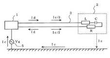
図12は、自動車用のスマートエントリーシステムに用いられる従来の高周波磁界発生装置(車載機)の概略構成を示す図である。
また、図13は、図12に示した従来の高周波磁界発生装置に用いられるLF(Low Frequency)アンテナの構成を示す図である。
また、図14は、平衡化されていない従来の不平衡LF送信系を簡単化した等価回路を示す図である。
なお、スマートエントリーシステムとは、キー操作をすることなく自動車のドアロックを解除し、スムーズに乗車してワンタッチでスタートできる自動車用電子キーシステムのことである。
図12〜図14を用いて、従来の高周波磁界発生装置について説明する。FIG. 12 is a diagram showing a schematic configuration of a conventional high-frequency magnetic field generator (on-vehicle device) used in a smart entry system for automobiles.
FIG. 13 is a diagram showing a configuration of an LF (Low Frequency) antenna used in the conventional high-frequency magnetic field generator shown in FIG.
FIG. 14 is a diagram showing an equivalent circuit obtained by simplifying a conventional unbalanced LF transmission system that is not balanced.
The smart entry system is an electronic key system for automobiles that can be unlocked and started with one touch without releasing the door lock of the automobile without any key operation.
A conventional high-frequency magnetic field generator will be described with reference to FIGS.
高周波磁界発生装置(車載機)の制御回路基板1は、その内部に設けられた図示しないインバータによって、LF帯(132kHz)のアンテナである高周波磁界送信用アンテナ2に供給するための高周波電流パルスを生成する。
制御回路基板1で生成された高周波電流パルスは、高周波磁界送信用アンテナ2に伝送線路(ツイストペア線)3を介して送り込まれる。
高周波磁界送信用アンテナ2は、送り込まれた高周波電流パルスに基づいて高周波磁界(誘導磁場)を生成し、生成された高周波磁界を送信する。
携帯機は、内蔵するLF受信回路で高周波磁界(誘導磁場)を検出した場合に、返信用のUHF電波を返す。これにより、車内にあるスマートエントリーシステムは、携帯機が車内にあるか、車外にあるかを判定できる。The
The high frequency current pulse generated by the
The high-frequency magnetic
When the portable device detects a high-frequency magnetic field (inductive magnetic field) with the built-in LF receiver circuit, it returns a UHF radio wave for return. Thereby, the smart entry system in the vehicle can determine whether the portable device is in the vehicle or outside the vehicle.
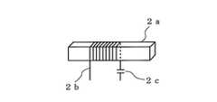
従来の高周波磁界発生装置に用いられる高周波磁界送信用アンテナ2は、図13に示すようにフェライト棒2aに巻回されたソレノイドコイル2bと該ソレノイドコイル2bに直列接続された共振用コンデンサ2cとで構成されている。
ソレノイドコイル2bはインダクタLと抵抗Rを有するので、従来の高周波磁界送信用アンテナ2は、図12に示すようにL、C、Rが直列接続されたものであり、その負荷ZはL、C、Rの直列インピーダンスとなる。
なお、図12において、Idはディファレンシャルモード電流、Icはコモンモード電流、Vgはコモンモード雑音電圧である。As shown in FIG. 13, a high frequency magnetic
Since the solenoid coil 2b has an inductor L and a resistor R, the conventional high-frequency magnetic
In FIG. 12, Id is a differential mode current, Ic is a common mode current, and Vg is a common mode noise voltage.
また、図14において、Vsは制御回路基板1の出力電圧、Vgはコモンモード雑音電圧、Zは高周波磁界送信用アンテナ2のインピーダンス、Zcは高周波磁界送信用アンテナ2と車体グランド間のインピーダンス、I1およびI2は伝送線路3上の電流である。電流の連続性から、車体グランドには、I1+I2の電流が流れる。
図14の等価回路の解析により、I1およびI2は次式で与えられる。
I1 = Vs/Z ・・・・・ (1)
I2 = −Vs/Z + Vg/Zc ・・・・ (2)
式(1)および式(2)より次式を得る。
I1+I2=Vg/Zc ・・・・・ (3)
なお、ここで、
I1= Id+Ic/2
I2= −Id+Ic/2
I1+I2 = Ic
である。In FIG. 14, Vs is the output voltage of the
From the analysis of the equivalent circuit of FIG. 14, I1 and I2 are given by the following equations.
I1 = Vs / Z (1)
I2 = −Vs / Z + Vg / Zc (2)
The following formula is obtained from formula (1) and formula (2).
I1 + I2 = Vg / Zc (3)
Where
I1 = Id + Ic / 2
I2 = −Id + Ic / 2
I1 + I2 = Ic
It is.
従来の高周波磁界発生装置の回路では、以下のような問題が生じる。
* 電源グランド側の伝送線路にもコモンモード電流Icが流れる。
* 電源のホット側の伝送線路および高周波磁界送信用アンテナにはディファレンシャルモード電流Idのみが流れる。
高周波磁界送信用アンテナがQの高い共振回路であっても、高調波が抑制されるのはディファレンシャルモード電流Idのみであり、コモンモード電流Icの高調波は抑制されない。
* コモンモード電流Icは、グランド側の伝送線とグランドを介して大ループを形成する。
* 負荷Zを除去(Z→∞)しても、式(2)により電源グランド側の伝送線とグランドにはコモンモード電流Icが流れ、伝送線路はループアンテナとして電界を生成する。The following problems occur in the circuit of the conventional high-frequency magnetic field generator.
* The common mode current Ic also flows through the transmission line on the power supply ground side.
* Only the differential mode current Id flows through the transmission line on the hot side of the power supply and the high frequency magnetic field transmitting antenna.
Even if the high-frequency magnetic field transmitting antenna is a resonance circuit having a high Q, the harmonics are suppressed only by the differential mode current Id, and the harmonics of the common mode current Ic are not suppressed.
* The common mode current Ic forms a large loop through the ground-side transmission line and the ground.
* Even if the load Z is removed (Z → ∞), the common mode current Ic flows through the transmission line and the ground on the power supply ground side according to Equation (2), and the transmission line generates an electric field as a loop antenna.
* 伝送線路をツイスト線にすれば、ディファレンシャルモード電流Idについては、ループ面積を極小化できるが、コモンモード電流Icについては、グランド面とツイスト線の間隔で決まるループ面積となり、ツイスト線の引き回しに大きく依存する電界を生成する。
したがって、コモンモード電流Icが小さくても、ループ面積が大きいため発生する電界強度は大きい。
なお、図13のアンテナにおけるループ電流Iが生成する電界強度Eは、次式で与えられる。
E= jωμSI/(4πr2)sinθ ・・・・・ (4)
ここで、Sはループ断面積、μはフェライトの透磁率、ωは角周波数であり、動作周波数fに対して、ω = 2πfで与えられる。
また、rはループ中心から電界強度観測点までの距離、θはループ断面の放線方向と観測点がなす角度である。* If the transmission line is a twisted line, the loop area can be minimized for the differential mode current Id, but the common mode current Ic has a loop area determined by the distance between the ground plane and the twisted line. Generates a highly dependent electric field.
Therefore, even if the common mode current Ic is small, the generated electric field strength is large because the loop area is large.
The electric field intensity E generated by the loop current I in the antenna of FIG. 13 is given by the following equation.
E = jωμSI / (4πr2 ) sin θ (4)
Here, S is the loop cross-sectional area, μ is the permeability of the ferrite, ω is the angular frequency, and is given by ω = 2πf with respect to the operating frequency f.
Further, r is the distance from the loop center to the field strength observation point, and θ is the angle formed by the observation direction and the normal direction of the loop cross section.
さらに、式(4)に示すようにループ電流による電界強度Eは、ωが乗算されるので、矩形波の高調波が1/ωの強度をもつことを考えると、電界の高調波レベルは減衰しないことになる。
さらに、コモンモード電流Icは共振負荷には流れず、対地容量に流れるため、共振回路による高調波減衰は期待できないことにも留意する必要がある。
* コモンモード電流Icが大きいと、伝送線路をツイストペア線としても往復電流が同一にならないので、漏れ電界が大きくなる。
即ち、平衡化していない不平衡LF送信系を用いた従来の高周波磁界発生装置は、コモンモード電流に起因する漏れ電界によって、中波帯のラジオ周波数に妨害電波を発生する。Furthermore, as shown in Equation (4), the electric field intensity E due to the loop current is multiplied by ω, so that the harmonic level of the electric field is attenuated considering that the harmonics of the rectangular wave have an intensity of 1 / ω. Will not.
Further, it should be noted that the harmonic attenuation by the resonance circuit cannot be expected because the common mode current Ic does not flow to the resonant load but flows to the ground capacitance.
* When the common mode current Ic is large, the round-trip currents are not the same even if the transmission line is a twisted pair wire, and the leakage electric field becomes large.
That is, a conventional high-frequency magnetic field generator using an unbalanced unbalanced LF transmission system generates a jamming radio wave at a radio frequency in the middle wave band due to a leakage electric field caused by a common mode current.
なお、スマートエントリーシステムの基本的な構成・動作については、下記の特許文献1に記載されているので参照されたい。
また、コモンモードノイズの発生原因、コモンモードノイズによる障害と対策、EMI(electro-magnetic interference:電磁波妨害)フィルタの構成と特性などについては、下記の非特許文献1に記載されているので参照されたい。
Further, the cause of common mode noise, the failure and countermeasures due to common mode noise, the configuration and characteristics of an EMI (electro-magnetic interference) filter, and the like are described in
以上述べたように、従来の高周波磁界発生装置(車載機)では、制御回路基板1の出力段が不平衡インピーダンス、伝送線路3がツイストペア線で平衡インピーダンス、高周波磁界送信用アンテナ2が平衡でも不平衡でもないインピーダンスであり、確実に平衡化されていない不平衡LF送信系を用いている。
従って、制御回路基板1内のインバータで生成され、LFアンテナ(高周波磁界送信用アンテナ2)に供給する高周波電流パルスのコモンモード電流に起因する漏れ電界によって、ラジオ周波数帯の妨害電波(高調波ノイズ)が発生する。
特に、車両の後部窓に埋め込まれたラジオ用アンテナ(通称ガラスアンテナと称す)に対して、その近傍に設置されるLFアンテナ(高周波磁界送信用アンテナ)からのラジオノイズが顕著であるという問題点があった。
この発明は、このような問題点を解決するためになされたもので、車載されたラジオに対する妨害電波(高調波ノイズ)の発生を大幅に低減でき、自動車用スマートエントリーシステムに適した高周波磁界発生装置を提供することを目的とする。As described above, in the conventional high-frequency magnetic field generator (on-vehicle device), the output stage of the
Therefore, the radio frequency band interference radio wave (harmonic noise) is generated by the leakage electric field generated by the common mode current of the high frequency current pulse generated by the inverter in the
In particular, radio noise from a LF antenna (high frequency magnetic field transmitting antenna) installed in the vicinity of a radio antenna (commonly called a glass antenna) embedded in the rear window of a vehicle is prominent. was there.
The present invention has been made to solve such problems, and can greatly reduce the generation of jamming radio waves (harmonic noise) with respect to a radio mounted on a vehicle, and generates a high-frequency magnetic field suitable for a smart entry system for automobiles. An object is to provide an apparatus.
この発明に係る高周波磁界発生装置は、複数のスイッチング素子によって形成されているブリッジ回路と、このブリッジ回路にDC電圧を印加するDC電源と、複数のスイッチング素子を所定の周波数でオン/オン制御することにより所定周波数の高周波電流パルスをブリッジ回路に発生させる制御回路部と、ブリッジ回路で発生した高周波電流パルスを伝送する伝送線路と、伝送線路を介して入力される高周波電流パルスに基づいて、高周波磁界を生成して送信する高周波磁界送信用アンテナを備え、伝送線路および高周波磁界送信用アンテナは平衡インピーダンス化されているものである。 A high-frequency magnetic field generator according to the present invention includes a bridge circuit formed by a plurality of switching elements, a DC power source that applies a DC voltage to the bridge circuit, and on / on-controlling the plurality of switching elements at a predetermined frequency. A control circuit unit for generating a high frequency current pulse of a predetermined frequency in the bridge circuit, a transmission line for transmitting the high frequency current pulse generated in the bridge circuit, and a high frequency current pulse based on the high frequency current pulse input through the transmission line A high frequency magnetic field transmitting antenna that generates and transmits a magnetic field is provided, and the transmission line and the high frequency magnetic field transmitting antenna are balanced impedance.
この発明による高周波磁界発生装置によれば、LF伝送系におけるコモンモードノイズが抑圧されるので、車載ラジオに対する妨害電波(高調波ノイズ)の発生を大幅に低減することが可能となり、自動車用スマートエントリーシステムに適した高周波磁界発生装置を実現できる。 According to the high-frequency magnetic field generator according to the present invention, since common mode noise in the LF transmission system is suppressed, it is possible to greatly reduce the generation of jamming radio waves (harmonic noise) with respect to the in-vehicle radio, and the smart entry for automobiles. A high-frequency magnetic field generator suitable for the system can be realized.
以下、図面に基づいて、本発明の一実施の形態について説明する。
なお、各図間において、同一符号は、同一あるいは相当のものを表す。
実施の形態1.
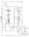
図1は、本発明の実施の形態1による高周波磁界発生装置(即ち、スマートエントリーシステムに用いられる車載機のLF送信装置)の概略構成を示す図である。
図において、10は制御回路基板、20はLF(LowFrequency)アンテナである高周波磁界送信用アンテナ、30は伝送線路であるツイストペア線、40は高周波用トランスであるフェライトトランス、50はコモンモード雑音電圧Vgである。
また、60はFET101〜FET104で形成されたフルブリッジ回路に第一のDC電圧(例えば、12V)を供給する第一のDC電源であり、70は後述する制御回路部100に第二のDC電圧(例えば、5V)を供給する第二のDC電源である。Hereinafter, an embodiment of the present invention will be described with reference to the drawings.
In addition, the same code | symbol represents the same or equivalent among each figure.
FIG. 1 is a diagram showing a schematic configuration of a high-frequency magnetic field generator (that is, an LF transmitter for an in-vehicle device used in a smart entry system) according to
In the figure, 10 is a control circuit board, 20 is a high frequency magnetic field transmitting antenna that is an LF (Low Frequency) antenna, 30 is a twisted pair wire that is a transmission line, 40 is a ferrite transformer that is a high frequency transformer, and 50 is a common mode noise voltage Vg. It is.
制御回路基板10は、後述する制御回路部100、フルブリッジ回路を形成する4つのスイッチング素子であるFET101〜FET104、スイッチング素子FET101〜FET104で形成されたフルブリッジ回路の出力部に配置された電流制限用の抵抗105と抵抗106、フルブリッジ回路の第一のDC電源60側に配置されたデカップリングコンデンサ(バイパスコンデンサ)109、110などを有している。
伝送系におけるディファレンシャルモード高調波は、高周波トランス(フェライトトランス)40では除去されず、そのまま負荷側(即ち、高周波磁界送信用アンテナ20側)に伝送されるため、別途対策が必要になる。
本実施の形態による高周波磁界発生装置の負荷(即ち、高周波磁界送信用アンテナ20)は直列共振回路であり、Q値が高ければ共振周波数より十分高い周波数におけるインピーダンスが上昇するため、高調波ノイズ電流が低減する。The
Since the differential mode harmonics in the transmission system are not removed by the high frequency transformer (ferrite transformer) 40 but are transmitted as they are to the load side (that is, the high frequency magnetic
The load of the high-frequency magnetic field generator according to the present embodiment (that is, the high-frequency magnetic field transmitting antenna 20) is a series resonance circuit, and if the Q value is high, the impedance at a frequency sufficiently higher than the resonance frequency increases. Is reduced.
しかしながら、負荷であるLFアンテナ(高周波磁界送信用アンテナ20)に流れる高調波電流が低減するだけであって、ツイストペア線である伝送線路30の線間容量に流れる高調波電流について抑制する効果はない。
この短絡電流(即ち、伝送線路40の線間容量に流れる高調波電流)を抑制するためには、制御回路基板12側にローパスフィルタを挿入して、伝送線路30の上流で高調波を短絡することが考えられる。
フルブリッジ回路の出力端間に配置されているコンデンサ107および108は、抵抗105と抵抗106によりローパスフィルタを形成しており、ディファレンシャルモード高調波を抑制できる。
ローパスフィルタの遮断周波数は、常識的には動作周波数(基本波周波数の132.45kHz)より高くするが、本実施の形態では、フィルタの傾斜特性をフルに利用するために、この遮断周波数を基本波周波数より低くし、高調波レベルを最大限抑制することができた。However, only the harmonic current flowing through the load LF antenna (high frequency magnetic field transmitting antenna 20) is reduced, and there is no effect of suppressing the harmonic current flowing through the line-to-line capacitance of the
In order to suppress this short-circuit current (ie, harmonic current flowing through the line-to-line capacitance of the transmission line 40), a low-pass filter is inserted on the
The cut-off frequency of the low-pass filter is commonly set higher than the operating frequency (132.45 kHz of the fundamental wave frequency), but in this embodiment, this cut-off frequency is set to the fundamental wave in order to make full use of the filter slope characteristics. The harmonic level could be suppressed to the maximum by making it lower than the frequency.
制御回路部100は、マイクロプロセッサ、ロジックIC、これらとフルブリッジ回路との間のインターフェースを行うインターフェース回路などで構成されており、種々のパルスを出力できるように構成されている。
そして、制御回路部100は、フルブリッジ回路を形成する各FET101〜104を所定のタイミングでオン/オフし、所定の周波数(例えば、132KHz)の高周波パルス電流を2ターン対2ターンの高周波トランス(フェライトトランス)40に出力する。
高周波トランス(フェライトトランス)40の出力側の高周波パルス電流は、伝送線路であるツイストペア線30を介して高周波磁界送信用アンテナ20に入力され、高周波磁界送信用アンテナ20は、所定周波数(132KHz)の高周波磁界を発生して送信する。The
Then, the
The high-frequency pulse current on the output side of the high-frequency transformer (ferrite transformer) 40 is input to the high-frequency magnetic
なお、制御回路部100は、所定の周波数(132KHz)の高周波パルス電流を発生させる際に、各車両に対応したID符号が所定の周波数(132KHz)の電波の中に含まれるようにしている。また、各種の暗号コードなどもこの電波の中に入れ込めるようになっている。
これにより、例えば、自分の車の横に同じスマートエントリーシステムを実装した同一車種の車が駐車していても、誤って他社の車のスマートエントリーシステムが動作しないようになっている。The
As a result, for example, even if a car of the same vehicle type having the same smart entry system mounted next to his / her car is parked, the smart entry system of another company's car does not operate by mistake.
また、図2は、図1に示した実施の形態1による高周波磁界発生装置に用いられるLF(Low Frequency)アンテナである高周波磁界送信用アンテナ20の具体的な構成を示す図である。
図において、21はフェライト棒、22は第一のソレノイドコイル、23は第二のソレノイドコイル、24は共振用コンデンサである。
図に示すように、高周波磁界送信用アンテナ20は、1本のフェライト棒21に第一のソレノイドコイル22および第二のソレノイドコイル23が巻回され、さらに第一のソレノイドコイル22と第二のソレノイドコイル23の間には共振用コンデンサ24が接続(配置)されており、これら第一のソレノイドコイル22、第二のソレノイドコイル23および共振用コンデンサ24は直列共振回路を形成している。FIG. 2 is a diagram showing a specific configuration of a high-frequency magnetic
In the figure, 21 is a ferrite rod, 22 is a first solenoid coil, 23 is a second solenoid coil, and 24 is a resonance capacitor.
As shown in the figure, the high-frequency magnetic
このように、本実施の形態による高周波磁界発生装置おいては、不平衡インピーダンスを有する制御回路基板10の出力に2ターン対2ターンの高周波トランス(フェライトトランス)40を配置して、コモンモード雑音Vgを遮断する。
さらに、高周波トランス(フェライトトランス)40からLFアンテナである高周波磁界送信用アンテナ20までは、ツイストペア線30で配線すると共に、高周波磁界送信用アンテナ20は直列共振アンテナとし、共振用コンデンサを2つのソレノイドコイル22、23のセンター位置に配置して対称構造とすることにより、高周波トランス(フェライトトランス)40の2次側インピーダンスを平衡化している。
なお、平衡とはグランド面に対してバランスしているという意味である。As described above, in the high-frequency magnetic field generator according to the present embodiment, the two-turn to two-turn high-frequency transformer (ferrite transformer) 40 is arranged at the output of the
Further, the high-frequency transformer (ferrite transformer) 40 to the high-frequency magnetic
In addition, the balance means that it is balanced with respect to the ground plane.
なお、図1に示した本実施の形態から判ることを纏めて述べると以下のようになる。
* 高周波トランス(フェライトトランス)40からLFアンテナである高周波磁界送信用アンテナ20までの回路が対称であれば、平衡線路であるツイストペア線30上の往復電流は反対称( I1 = −I2 )となる。したがって、往復電流により生成される電界を最小にできる。
* また、回路の対称性が十分であれば、I1 +I2 = 0 となり、グランドには電流が流れない。したがって、アンテナ負荷を除去すると、高調波雑音を発生しない。
* ディファレンシャルモード電流が支配的になるため、さらなる高調波抑制のためには、共振系のQ値を増大させればよい。
*図1の回路において、もしもアンテナ負荷の対称性を悪化させた場合、伝送線路および負荷全体が平衡しているという仮定が崩れるため、I1 +I2 = 0 を保障できない。したがって、コモンモード電流が生成される。
このため、高周波磁界送信用アンテナ20において、ソレノイドコイルを2分割して第一のソレノイドコイル22および第二のソレノイドコイル23とし、その間に共振用コンデンサ24を配置している。Note that what can be understood from the present embodiment shown in FIG. 1 is summarized as follows.
* If the circuit from the high-frequency transformer (ferrite transformer) 40 to the high-frequency magnetic
* If the circuit has sufficient symmetry, I1 + I2 = 0 and no current flows through the ground. Therefore, no harmonic noise is generated when the antenna load is removed.
* Since the differential mode current becomes dominant, the Q value of the resonance system may be increased in order to further suppress harmonics.
* In the circuit of FIG. 1, if the symmetry of the antenna load is deteriorated, the assumption that the transmission line and the entire load are balanced cannot be guaranteed, so that I1 + I2 = 0 cannot be guaranteed. Therefore, a common mode current is generated.
For this reason, in the high-frequency magnetic
ところで、高周波磁界発生装置の制御回路基板には、所定周波数の高周波電流パルスを発生するためのインバータの出力部として、スイッチング素子である4つのFET(FET101〜FET104)を用いたフルブリッジ回路が設けられている。
このフルブリッジ回路は片側グランドであるが、インバータの半周期ごとに電流が逆流する対称回路となっている。
ところが、出力電流を制限するための抵抗を不用意に出力部に挿入すると、回路の平衡が崩れて出力ケーブルのグランド電位が変動し、コモンモードの電圧を生成する。
例えば、図3に示すように、フルブリッジ回路出力の片側に10Ωの電流制限用の抵抗111を挿入して、1Aの電流を通電した場合、新たに10Vのコモンモードのスイッチング電源が接続されたことになり、その影響は大きい。By the way, the control circuit board of the high-frequency magnetic field generator is provided with a full bridge circuit using four FETs (FET101 to FET104) as switching elements as an output part of an inverter for generating a high-frequency current pulse of a predetermined frequency. It has been.
This full bridge circuit is a ground on one side, but is a symmetric circuit in which current flows backward every half cycle of the inverter.
However, if a resistor for limiting the output current is inadvertently inserted into the output section, the circuit is unbalanced and the ground potential of the output cable fluctuates, generating a common mode voltage.
For example, as shown in FIG. 3, when a 10 Ω current limiting
図3は、FETによるフルブリッジ回路出力の片側に電流制限用の抵抗111を挿入した場合を示す図である。図3を用いて、電流制限用の抵抗111を挿入した場合の影響について説明する。
高周波トランス(フェライトトランス)40における線路電位を、それぞれV1、V2とし、電流制限用の抵抗111の抵抗値をR、通電電流をI、FET駆動用のDC電源である第一のDC電源60の出力電圧をvとする。
図3から、V1、V2は次式で表される。
ブリッジの位相0〜180度 : V1 = v−IR、V2 = 0 ・・・ (5)
ブリッジの位相180〜360度 : V1 = IR、V2 = v ・・・ (6)FIG. 3 is a diagram showing a case where a current limiting
The line potentials in the high-frequency transformer (ferrite transformer) 40 are V1 and V2, respectively, the resistance value of the current limiting
From FIG. 3, V1 and V2 are expressed by the following equations.
Bridge phase 180-360 degrees: V1 = IR, V2 = v (6)
次に、上記線路電位(V1、V2)をコモンモードとディファレンシャルモードに分解する。
図4に平衡線路におけるコモンモード電源とディファレンシャルモード電源の等価回路モデルを示す。
図4から明らかなように、コモンモード電源電圧Vc、ディファレンシャルモード電源電圧Vdと線路電位V1、V2の関係は次式で与えられる。
V1= Vc+Vd/2、 V2 = Vc−Vd/2 ・・・ (7)
即ち、
Vc= (V1+V2)/2、 Vd = V1−V2 ・・・ (8)Next, the line potential (V1, V2) is decomposed into a common mode and a differential mode.
FIG. 4 shows an equivalent circuit model of a common mode power source and a differential mode power source in a balanced line.
As is apparent from FIG. 4, the relationship among the common mode power supply voltage Vc, the differential mode power supply voltage Vd and the line potentials V1 and V2 is given by the following equation.
V1 = Vc + Vd / 2, V2 = Vc−Vd / 2 (7)
That is,
Vc = (V1 + V2) / 2, Vd = V1-V2 (8)
式(5)、式(6)、式(8)から次式を得る。
ブリッジの位相0〜180度 :
Vc = (v−IR)/2、 Vd =v−IR ・・・ (9)
ブリッジの位相180〜360度 :
Vc = (v+IR)/2、 Vd =IR−v ・・・(10)The following expression is obtained from Expression (5), Expression (6), and Expression (8).
Vc = (v-IR) / 2, Vd = v-IR (9)
Bridge phase 180-360 degrees:
Vc = (v + IR) / 2, Vd = IR−v (10)
(9)式および(10)式からわかるように、Vdは前半位相と後半位相で反転する正常なディファレンシャルスイッチング電源である。
一方、Vcは抵抗Rがゼロでない限り、半周期ごとに値が変動し、交流成分としては、Vc = IRとなる。
すなわち、大きな電流制限抵抗を2次側に挿入すると、大きなコモンモードのスイッチング電源を接続したことになり、ノイズ源となってしまうことがわかった。
電流1A、抵抗10Ωでは、このノイズ電源電圧が10Vにも達する。このような大振幅を有するコモンモードノイズは、たとえフェライトトランスを挿入して回路を平衡化しても、トランスの1次、2次間の静電結合や回路の平衡性の不完全さを考えれば、完全に除去することは困難である。
対策としては、電流制限抵抗は十分抵抗値がそろったペア抵抗を線路の両側に挿入して完全に平衡インピーダンス化するか、1つの抵抗で電流制限できるように回路を工夫することが有効である。As can be seen from the equations (9) and (10), Vd is a normal differential switching power supply that is inverted between the first half phase and the second half phase.
On the other hand, as long as the resistance R is not zero, the value of Vc fluctuates every half cycle, and the AC component is Vc = IR.
That is, when a large current limiting resistor is inserted on the secondary side, a large common mode switching power supply is connected, which is a noise source.
With a current of 1A and a resistance of 10Ω, this noise power supply voltage reaches 10V. Even if a ferrite transformer is inserted and the circuit is balanced, the common mode noise having such a large amplitude can be considered if the primary coupling and the secondary coupling of the transformer or imbalance of the circuit is considered. It is difficult to remove completely.
As a countermeasure, it is effective to devise a circuit so that the current limiting resistor can be completely balanced impedance by inserting pair resistors with sufficient resistance values on both sides of the line, or the current can be limited by one resistor. .
ここで、本実施の形態による高周波磁界発生装置のコモンモードノイズの低減効果について検証したので、その結果について説明しておく。
図5は、高周波磁界発生装置のLFアンテナ(高周波磁界送信用アンテナ20)から送信される高周波磁界の車載ラジオアンテナ端における電界スペクトルの測定系を示す図である。
電波暗室200内において高周波磁界送信用アンテナ20をセダン車のリアトレイ位置に設置し、車載AMラジオ202の受信アンテナであるガラスアンテナ201の出力ケーブルをインピーダンス変換器203に接続し、プリアンプ204で増幅した後、スペアナ205とPC(パソコン)206とで構成されるEMI測定システムに入力した。Here, since the reduction effect of the common mode noise of the high frequency magnetic field generator according to the present embodiment has been verified, the result will be described.
FIG. 5 is a diagram showing a measurement system of an electric field spectrum at the end of the in-vehicle radio antenna of the high frequency magnetic field transmitted from the LF antenna (high frequency magnetic field transmitting antenna 20) of the high frequency magnetic field generator.
In the anechoic chamber 200, the high-frequency magnetic
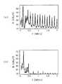
図6は、本実施の形態による高周波磁界発生装置のコモンモードノイズ低減効果を説明するための図である。
図6(a)は、LFコイルの片側に共振コンデンサを配置した不平衡LFアンテナ(高周波磁界送信用アンテナ)をツイストペア線で制御回路基板に接続した従来の高周波磁界発生装置におけるラジオアンテナ端電圧スペクトルを示す。
図6(a)では、全体的に高調波のレベルが高く、高調波の次数増大に伴う振幅減衰が緩慢である。
さらに、LFアンテナを駆動する電流パルス(図3の電流I)のデューティサイクルが約50%であるにもかかわらず、偶数次高調波が存在するため、この偶数次高調波はコモンモード電流に由来すると考えざるを得ない。
コモンモード電界は、周波数特性がフラットになるため、高調波ノイズが顕著であり、できるだけ抑制する必要がある。FIG. 6 is a diagram for explaining the common mode noise reduction effect of the high-frequency magnetic field generator according to the present embodiment.
FIG. 6A shows a voltage spectrum at the end of a radio antenna in a conventional high frequency magnetic field generator in which an unbalanced LF antenna (high frequency magnetic field transmitting antenna) having a resonant capacitor arranged on one side of an LF coil is connected to a control circuit board by a twisted pair wire. Indicates.
In FIG. 6A, the harmonic level is generally high, and the amplitude attenuation accompanying the increase in the harmonic order is slow.
In addition, even harmonics are present despite the duty cycle of the current pulse driving the LF antenna (current I in FIG. 3) is about 50%, so this even harmonic is derived from the common mode current. Then I have to think about it.
Since the frequency characteristics of the common mode electric field are flat, harmonic noise is remarkable and should be suppressed as much as possible.
これに対して、図1に示した実施の形態1による高周波磁界発生装置のように、フェライトトランス(高周波トランス40)とバランス型LFアンテナ(即ち、図1あるいは図2に示した高周波磁界送信用アンテナ20)によるコモンモードノイズ抑制対策後のラジオアンテナ電圧スペクトルを図6(b)に示す。
高調波が約30dB程度抑制されると共に、偶数次高調波レベルが奇数次高調波レベルに比較して十分減衰している。
これは、コモンモード電流が抑制されたため、共振回路に流れるディファレンシャルモード電流の特性を反映して奇数次高調波が理論どおりQ値に従って減衰していることを示していると考えられる。
また、図6(b)は、LFアンテナを駆動する電流パルスのデューティサイクルが約50%では偶数次高調波が発生しないという理論を支持する結果にもなっている。On the other hand, as in the high-frequency magnetic field generator according to
Harmonics are suppressed by about 30 dB, and even-order harmonic levels are sufficiently attenuated compared to odd-order harmonic levels.
This is considered to indicate that the odd-order harmonics are attenuated according to the Q value as theoretically reflecting the characteristics of the differential mode current flowing in the resonance circuit because the common mode current is suppressed.
FIG. 6B also supports the theory that even-order harmonics do not occur when the duty cycle of the current pulse for driving the LF antenna is about 50%.
次に、本実施の形態におけるローパスフィルタの効果の検証結果について述べる。
図7は、前掲の図5に示した測定系を用いて、図1に示した本実施の形態による高周波磁界発生装置(フルブリッジ回路の出力側端部に挿入される抵抗105、106を有している)のアンテナ端電圧の周波数スペクトルを測定した結果を示している。
また、図8は、図1に示した本実施の形態による高周波磁界発生装置の規定周波数におけるアンテナ端電圧のスペクトル強度とラジオのスピーカ端電圧を示したものである。
なお、図8において、F4、F5、F6、・・・は、それぞれ第4次高調波周波数、第5次高調波周波数、第6次高調波周波数、・・・を表している。
図8に示すごとく、高調波スペクトル強度が大きい周波数では、スピーカノイズも大きいことがわかる。Next, the verification result of the effect of the low-pass filter in this embodiment will be described.
FIG. 7 shows a high-frequency magnetic field generator according to the present embodiment shown in FIG. 1 (having
FIG. 8 shows the spectrum intensity of the antenna end voltage and the radio speaker end voltage at the specified frequency of the high-frequency magnetic field generator according to the present embodiment shown in FIG.
In FIG. 8, F4, F5, F6,... Represent a fourth harmonic frequency, a fifth harmonic frequency, a sixth harmonic frequency,.
As shown in FIG. 8, it can be seen that loudspeaker noise is large at frequencies where the harmonic spectrum intensity is large.
以上説明したように、本実施の形態による高周波磁界発生装置は、複数のスイッチング素子(FET101〜FET104)によって形成されているブリッジ回路と、このブリッジ回路にDC電圧を印加するDC電源60と、複数のスイッチング素子(FET101〜FET104)を所定の周波数でオン/オン制御することにより所定周波数の高周波電流パルスを上記ブリッジ回路に発生させる制御回路部100と、上記ブリッジ回路で発生した高周波電流パルスを伝送する伝送線路30と、伝送線路30を介して入力される高周波電流パルスに基づいて、高周波磁界を生成して送信する高周波磁界送信用アンテナ20を備え、伝送線路30および高周波磁界送信用アンテナ20は平衡インピーダンス化されている。
従って、伝送系におけるコモンモードノイズが抑圧されるので、車載されたラジオに対する妨害電波(高調波ノイズ)の発生を大幅に低減することが可能となり、自動車用スマートエントリーシステムに適した高周波磁界発生装置を実現できる。As described above, the high-frequency magnetic field generator according to the present embodiment includes a bridge circuit formed by a plurality of switching elements (FET101 to FET104), a
Therefore, since common mode noise in the transmission system is suppressed, it is possible to significantly reduce the generation of jamming radio waves (harmonic noise) on the vehicle-mounted radio, and a high-frequency magnetic field generator suitable for a smart entry system for automobiles. Can be realized.
また、本実施の形態による高周波磁界発生装置は、複数のスイッチング素子によって形成されているブリッジ回路の出力端と伝送線路30の間に、平衡インピーダンス化された高周波トランス40を設けているので、コモンモード雑音Vgを遮断することが可能となり、車載ラジオへ混入する高調はノイズを更に低減できる。
また、本実施の形態による高周波磁界発生装置の伝送線路40は、ツイストペア線であるので、伝送系におけるコモンモードノイズが更に抑圧されるので、車載されたラジオに対する妨害電波(高調波ノイズ)の発生を更に低減することができる。
また、本実施の形態による高周波磁界発生装置の高周波磁界送信用アンテナは、フェライト棒に巻回された第一のソレノイドコイルと第二のソレノイドコイル、および上記第一のソレノイドコイルと上記第二のソレノイドコイルの間に配置(接続)された共振用コイルで構成され、上記第一のソレノイドコイル、上記第二のソレノイドコイルおよび上記共振用コイルは直列共振回路を形成しているので、高周波磁界送信用アンテナの平衡化が図れ、コモンモードノイズが抑圧されて車載されたラジオに対する妨害電波(高調波ノイズ)の発生を低減することができる。In addition, the high-frequency magnetic field generator according to the present embodiment includes the high-
In addition, since the
The high frequency magnetic field transmitting antenna of the high frequency magnetic field generator according to the present embodiment includes a first solenoid coil and a second solenoid coil wound around a ferrite rod, and the first solenoid coil and the second solenoid coil. Since the first solenoid coil, the second solenoid coil, and the resonance coil form a series resonance circuit, they are arranged (connected) between the solenoid coils. The balance of the trust antenna can be achieved, and the occurrence of interference radio waves (harmonic noise) with respect to the radio mounted on the vehicle can be reduced by suppressing the common mode noise.
実施の形態2.
図9は、本発明の実施の形態2による高周波磁界発生装置の概略構成を示す図である。
本実施の形態による高周波磁界発生装置は、前述の実施の形態1による高周波磁界発生装置において、電流制限用抵抗105、106を除去して、DC電源60の正極側端子と接続されるブリッジ回路の端部に単一の抵抗122を直列に接続(配置)したことを特徴とする。
前述の実施の形態1による高周波磁界発生装置では、フルブリッジ回路の出力端側の両側に電流制限用の抵抗を設置していた。
従って、抵抗値のばらつきにより各線路のグランドから見た電位が非対称になり、その結果、ノイズ電圧が増大する。
そこで、電流制限抵抗を1つにする新方式を考案したので説明する。
本実施の形態では、図9に示すように、電流制限の機能を有する抵抗122をスイッチング素子である4個のFETで構成されたフルブリッジ回路の上流の電源ラインに挿入して、1つにまとめている。
即ち、電流制限の機能を有する抵抗は、抵抗122のみである。
さらに、ローパスフィルタ用のコンデンサCを制御回路基板12裏のFETに接近したピン位置で半田付けしている。
FIG. 9 is a diagram showing a schematic configuration of a high-frequency magnetic field generator according to
The high frequency magnetic field generator according to the present embodiment is the same as the high frequency magnetic field generator according to the first embodiment described above except that the current limiting
In the high-frequency magnetic field generator according to the first embodiment described above, current limiting resistors are provided on both sides on the output end side of the full bridge circuit.
Therefore, the potential viewed from the ground of each line becomes asymmetric due to the variation in resistance value, and as a result, the noise voltage increases.
Therefore, a new system that uses one current limiting resistor has been devised.
In the present embodiment, as shown in FIG. 9, a
That is, only the
Further, a low-pass filter capacitor C is soldered at a pin position close to the FET on the back of the
前述の実施の形態1による高周波磁界発生装置は、フルブリッジ回路を構成するFETに電源電圧が直接印加されていた。
しかし、本実施の形態による高周波磁界発生装置では、FETフルブリッジ回路の出力端に電流制限用抵抗を配置することを止めると共に、4つのFETで構成されたフルブリッジ回路の第一のDC電源の正極側端部に抵抗122を直列に接続(配置)している。
また、第一のDC電源からのDC電源が印加されるフルブリッジ回路のDC電源側端子間にはデカップリングコンデンサ109、110が設けられている。
このように、本実施の形態では、フルブリッジ回路の第一のDC電源60の正極側端部に接続される端子側に直列に配置された抵抗122と、フルブリッジ回路の出力側の端子間に配置されたコンデンサ107、108によって、フィルタ(RCフィルタ)が構成されている。
また、前述したように、電流制限用の抵抗として、抵抗122のみが配置されている。In the high-frequency magnetic field generator according to the first embodiment described above, the power supply voltage is directly applied to the FET constituting the full bridge circuit.
However, in the high-frequency magnetic field generator according to the present embodiment, the arrangement of the current limiting resistor at the output end of the FET full-bridge circuit is stopped, and the first DC power supply of the full-bridge circuit composed of four FETs is stopped. A
Further,
Thus, in this embodiment, the
Further, as described above, only the
以上説明したように、本実施の形態による高周波磁界発生装置は、ブリッジ回路の出力端と伝送線路30との間にコンデンサ107、108が設けられていると共に、DC電源60の正極側端子と接続されるブリッジ回路の端部に単一の抵抗122を直列に配置してローパスフィルタが構成されている。
抵抗が単一のため、抵抗値のバラツキによるコモンモードノイズの発生がなく、且つ、ディファレンシャルモードの高調波抑制することができ、車載ラジオに対する妨害電波(高調波ノイズ)の発生を更に低減することができる。
また、本実施の形態による高周波磁界発生装置の上記ローパスフィルタの遮断周波数は、高周波電流パルスの基本周波数よりも低く設定されているので、ローパスフィルタの傾斜特性をフルに(有効に)利用することが可能となり、高調波レベルを最大限に抑制することができる。As described above, the high-frequency magnetic field generator according to the present embodiment is provided with the
Since there is a single resistor, there is no occurrence of common mode noise due to variations in resistance value, and harmonics in the differential mode can be suppressed, further reducing the occurrence of jamming radio waves (harmonic noise) for in-vehicle radios. Can do.
In addition, since the cutoff frequency of the low-pass filter of the high-frequency magnetic field generator according to the present embodiment is set lower than the fundamental frequency of the high-frequency current pulse, the slope characteristics of the low-pass filter must be fully utilized. And the harmonic level can be suppressed to the maximum.
実施の形態3.
図10は、実施の形態3による高周波磁界発生装置の概略構成を示す図である。
図に示すように、本実施の形態では、抵抗133の前にインダクタンス132が追加されている。
その結果、ローパスフィルタがRL−Cフィルタとなり、高調波の減衰が大きくなる。
また、図11は、図1、図9、図10に示した実施の形態1、2、3による高周波磁界発生装置の規定周波数におけるアンテナ端電圧のスペクトル強度とスピーカ端電圧を示したものである。
なお、図11において、F4、F5、F6、・・・は、それぞれ第4次高調波周波数、第5次高調波周波数、第6次高調波周波数、・・・を表している。
図11から判るように、実施の形態2では、電流制限用抵抗を単一の抵抗122とすることにより、偶数次高調波、特に、4次高調波(F4)ノイズを1桁低減することができた。
また、実施の形態3では、インダクタ132の追加により、さらなる特性改善が可能になった。
FIG. 10 is a diagram showing a schematic configuration of the high-frequency magnetic field generator according to the third embodiment.
As shown in the figure, in this embodiment, an
As a result, the low-pass filter becomes an RL-C filter, and harmonic attenuation increases.
FIG. 11 shows the spectrum intensity of the antenna end voltage and the speaker end voltage at the specified frequency of the high-frequency magnetic field generator according to the first, second, and third embodiments shown in FIGS. .
In FIG. 11, F4, F5, F6,... Represent the fourth harmonic frequency, the fifth harmonic frequency, the sixth harmonic frequency,.
As can be seen from FIG. 11, in the second embodiment, the current limiting resistor is a
In the third embodiment, the characteristics can be further improved by adding the
以上説明したように、本実施の形態による高周波磁界発生装置は、ブリッジ回路の出力端間にローパス用コンデンサ131を設けると共に、DC電源60の正極側端子と接続されるブリッジ回路の端部にインダクタ132と抵抗133を直列に配置し、ローパス用コンデンサ131、インダクタ132および抵抗133とによってフィルタ(RL−Cフィルタ)を構成している。
その結果、電流制限抵抗は1つに纏められているので、偶数次高調波、特に4次高調波(F4)ノイズを大幅に低減減することができる。従って、車載ラジオに対する妨害電波(高調波ノイズ)の発生を更に低減することが可能となる。As described above, the high-frequency magnetic field generator according to the present embodiment has the low-
As a result, since the current limiting resistors are combined into one, even-order harmonics, particularly fourth-order harmonic (F4) noise can be greatly reduced. Accordingly, it is possible to further reduce the generation of interference radio waves (harmonic noise) with respect to the in-vehicle radio.
この発明は、車載されたラジオに対する妨害電波(高調波ノイズ)の発生を大幅に低減でき、自動車用スマートエントリーシステムに適した高周波磁界発生装置の実現に有用である。 INDUSTRIAL APPLICABILITY The present invention can greatly reduce the generation of jamming radio waves (harmonic noise) with respect to an on-vehicle radio, and is useful for realizing a high-frequency magnetic field generator suitable for an automobile smart entry system.
10、11、12、13 制御回路基板
20 高周波磁界送信用アンテナ
21 フェライト棒
22 第一のソレノイドコイル
23 第二のソレノイドコイル
24 共振用コンデンサ
30 伝送線路(ツイストペア線)
40 高周波トランス
50 コモンモード雑音
60 第一のDC電源
70 第二のDC電源
100 制御回路部
101、102、103、104 FET
105、106、111、122、133 抵抗
107、108、109、110 コンデンサ
131、134 コンデンサ
132 インダクタ10, 11, 12, 13
40 High-
105, 106, 111, 122, 133
Claims (7)
Translated fromJapanese上記ブリッジ回路にDC電圧を印加するDC電源と、
上記複数のスイッチング素子を所定の周波数でオン/オン制御することにより所定周波数の高周波電流パルスを上記ブリッジ回路に発生させる制御回路部と、
上記ブリッジ回路で発生した上記高周波電流パルスを伝送する伝送線路と、
上記伝送線路を介して入力される上記高周波電流パルスに基づいて、高周波磁界を生成して送信する高周波磁界生成用アンテナを備え、
上記伝送線路および上記高周波磁界生成用アンテナは、平衡インピーダンス化されていることを特徴とする高周波磁界発生装置。A bridge circuit formed by a plurality of switching elements;
A DC power source for applying a DC voltage to the bridge circuit;
A control circuit unit for generating a high-frequency current pulse of a predetermined frequency in the bridge circuit by performing on / on control of the plurality of switching elements at a predetermined frequency;
A transmission line for transmitting the high-frequency current pulse generated in the bridge circuit;
Based on the high-frequency current pulse input through the transmission line, a high-frequency magnetic field generating antenna that generates and transmits a high-frequency magnetic field,
The transmission line and the high-frequency magnetic field generating antenna are balanced impedances.
上記第一のソレノイドコイル、上記第二のソレノイドコイルおよび上記共振用コイルは直列共振回路を形成していることを特徴とする請求項1に記載の高周波磁界発生装置。The high frequency magnetic field generating antenna includes a first solenoid coil and a second solenoid coil wound around a ferrite rod, and a resonance coil disposed between the first solenoid coil and the second solenoid coil. Consists of
2. The high frequency magnetic field generator according to claim 1, wherein the first solenoid coil, the second solenoid coil, and the resonance coil form a series resonance circuit.
Priority Applications (1)
| Application Number | Priority Date | Filing Date | Title |
|---|---|---|---|
| JP2004215169AJP2006041652A (en) | 2004-07-23 | 2004-07-23 | High frequency magnetic field generator |
Applications Claiming Priority (1)
| Application Number | Priority Date | Filing Date | Title |
|---|---|---|---|
| JP2004215169AJP2006041652A (en) | 2004-07-23 | 2004-07-23 | High frequency magnetic field generator |
Publications (1)
| Publication Number | Publication Date |
|---|---|
| JP2006041652Atrue JP2006041652A (en) | 2006-02-09 |
Family
ID=35906206
Family Applications (1)
| Application Number | Title | Priority Date | Filing Date |
|---|---|---|---|
| JP2004215169APendingJP2006041652A (en) | 2004-07-23 | 2004-07-23 | High frequency magnetic field generator |
Country Status (1)
| Country | Link |
|---|---|
| JP (1) | JP2006041652A (en) |
Cited By (5)
| Publication number | Priority date | Publication date | Assignee | Title |
|---|---|---|---|---|
| JP2008022233A (en)* | 2006-07-12 | 2008-01-31 | Denso Corp | Open trouble detector of antenna and radio transmitter |
| JP2015049203A (en)* | 2013-09-04 | 2015-03-16 | 独立行政法人情報通信研究機構 | Common mode conducted disturbance measurement equipment |
| WO2018186408A1 (en)* | 2017-04-06 | 2018-10-11 | 株式会社村田製作所 | Magnetic field generation circuit |
| JP2018183028A (en)* | 2017-04-06 | 2018-11-15 | 株式会社村田製作所 | Magnetic field generation circuit |
| WO2019058982A1 (en)* | 2017-09-19 | 2019-03-28 | 株式会社オートネットワーク技術研究所 | In-vehicle device |
- 2004
- 2004-07-23JPJP2004215169Apatent/JP2006041652A/enactivePending
Cited By (6)
| Publication number | Priority date | Publication date | Assignee | Title |
|---|---|---|---|---|
| JP2008022233A (en)* | 2006-07-12 | 2008-01-31 | Denso Corp | Open trouble detector of antenna and radio transmitter |
| JP2015049203A (en)* | 2013-09-04 | 2015-03-16 | 独立行政法人情報通信研究機構 | Common mode conducted disturbance measurement equipment |
| WO2018186408A1 (en)* | 2017-04-06 | 2018-10-11 | 株式会社村田製作所 | Magnetic field generation circuit |
| JP2018183028A (en)* | 2017-04-06 | 2018-11-15 | 株式会社村田製作所 | Magnetic field generation circuit |
| US11404787B2 (en) | 2017-04-06 | 2022-08-02 | Murata Manufacturing Co., Ltd. | Magnetic-field generating circuit |
| WO2019058982A1 (en)* | 2017-09-19 | 2019-03-28 | 株式会社オートネットワーク技術研究所 | In-vehicle device |
Similar Documents
| Publication | Publication Date | Title |
|---|---|---|
| TWI232037B (en) | Noise suppressing circuit | |
| US7804188B2 (en) | Termination circuit, vehicle-mounted control apparatus, and vehicle-mounted communication system | |
| JP2008244701A (en) | Power line communication system | |
| KR20150071574A (en) | Low voltage electromagnetic interference filter of electric vehicle | |
| KR20100075314A (en) | Noise filter and motor control device having same | |
| EP1492287B1 (en) | Receiver for eliminating common mode noise in a differential signal | |
| US11951851B2 (en) | Switching device for a coil | |
| WO2012176832A1 (en) | Communication system and communication device | |
| US20110234337A1 (en) | Filter circuit for differential communication | |
| JP2006041652A (en) | High frequency magnetic field generator | |
| JP2002252521A (en) | Loop antenna device | |
| Jeschke et al. | Vehicle modelling during emission measurement of wireless charging stations using a passive impedance network | |
| US9564934B2 (en) | Telecontrol for automobile comprising a device for suppressing magnetic coupling | |
| JP2008079386A (en) | Automotive power supply | |
| US10164315B2 (en) | Apparatuses and methods for signal coupling | |
| JP2013038760A (en) | Communication system and communication device | |
| KR102498927B1 (en) | Radiofrequency transmission device | |
| US10050678B2 (en) | Radiofrequency transmission device | |
| CN106026073A (en) | Potential-free DC voltage network | |
| JP2012105081A (en) | High frequency noise filter for on-vehicle equipment, and filter connection method | |
| US11831170B2 (en) | Signal matching apparatus in a system for inductive power transmission | |
| CN114728630B (en) | Apparatus for a vehicle to communicate with a mobile device | |
| US11283485B2 (en) | Circuit for signal connection, device for inductive power transfer and for signal transmission | |
| Marksell | EMC aspects of PWM controlled loads in vehicles | |
| JP4843054B2 (en) | Communication device |
Legal Events
| Date | Code | Title | Description |
|---|---|---|---|
| A621 | Written request for application examination | Free format text:JAPANESE INTERMEDIATE CODE: A621 Effective date:20061220 | |
| A977 | Report on retrieval | Free format text:JAPANESE INTERMEDIATE CODE: A971007 Effective date:20081203 | |
| A131 | Notification of reasons for refusal | Free format text:JAPANESE INTERMEDIATE CODE: A131 Effective date:20081209 | |
| A02 | Decision of refusal | Free format text:JAPANESE INTERMEDIATE CODE: A02 Effective date:20090407 |