JP2006030439A - Liquid crystal device, method for manufacturing liquid crystal device, and electronic apparatus - Google Patents
Liquid crystal device, method for manufacturing liquid crystal device, and electronic apparatusDownload PDFInfo
- Publication number
- JP2006030439A JP2006030439AJP2004206976AJP2004206976AJP2006030439AJP 2006030439 AJP2006030439 AJP 2006030439AJP 2004206976 AJP2004206976 AJP 2004206976AJP 2004206976 AJP2004206976 AJP 2004206976AJP 2006030439 AJP2006030439 AJP 2006030439A
- Authority
- JP
- Japan
- Prior art keywords
- liquid crystal
- substrate
- sealing material
- crystal device
- groove
- Prior art date
- Legal status (The legal status is an assumption and is not a legal conclusion. Google has not performed a legal analysis and makes no representation as to the accuracy of the status listed.)
- Withdrawn
Links
- 239000004973liquid crystal related substanceSubstances0.000titleclaimsabstractdescription219
- 238000000034methodMethods0.000titleclaimsabstractdescription91
- 238000004519manufacturing processMethods0.000titleclaimsdescription58
- 239000000758substrateSubstances0.000claimsabstractdescription284
- 239000003566sealing materialSubstances0.000claimsabstractdescription182
- 238000005192partitionMethods0.000claimsabstractdescription125
- 239000000463materialSubstances0.000claimsdescription60
- 125000006850spacer groupChemical group0.000claimsdescription19
- 238000005520cutting processMethods0.000claimsdescription6
- 238000002347injectionMethods0.000description28
- 239000007924injectionSubstances0.000description28
- 230000008569processEffects0.000description24
- 230000004888barrier functionEffects0.000description9
- 239000007788liquidSubstances0.000description6
- 239000000853adhesiveSubstances0.000description5
- 230000001070adhesive effectEffects0.000description5
- 239000011248coating agentSubstances0.000description5
- 238000000576coating methodMethods0.000description5
- 239000011159matrix materialSubstances0.000description5
- 230000002093peripheral effectEffects0.000description5
- 239000012535impuritySubstances0.000description4
- 230000003287optical effectEffects0.000description4
- 238000000206photolithographyMethods0.000description4
- 238000007639printingMethods0.000description4
- 239000000565sealantSubstances0.000description4
- 239000002699waste materialSubstances0.000description4
- 239000004642PolyimideSubstances0.000description3
- 238000010586diagramMethods0.000description3
- 239000003822epoxy resinSubstances0.000description3
- 239000011521glassSubstances0.000description3
- 230000001771impaired effectEffects0.000description3
- 239000004033plasticSubstances0.000description3
- 229920000647polyepoxidePolymers0.000description3
- 229920001721polyimidePolymers0.000description3
- 238000007789sealingMethods0.000description3
- 239000004065semiconductorSubstances0.000description3
- 230000015572biosynthetic processEffects0.000description2
- 230000000903blocking effectEffects0.000description2
- 239000004020conductorSubstances0.000description2
- 239000000470constituentSubstances0.000description2
- 230000000694effectsEffects0.000description2
- 238000005530etchingMethods0.000description2
- 238000010438heat treatmentMethods0.000description2
- 238000000059patterningMethods0.000description2
- 229920005989resinPolymers0.000description2
- 239000011347resinSubstances0.000description2
- 238000007650screen-printingMethods0.000description2
- 238000009751slip formingMethods0.000description2
- 238000004544sputter depositionMethods0.000description2
- 238000004140cleaningMethods0.000description1
- 238000005429filling processMethods0.000description1
- 239000010419fine particleSubstances0.000description1
- 239000003365glass fiberSubstances0.000description1
- 230000002452interceptive effectEffects0.000description1
- 239000002184metalSubstances0.000description1
- 238000012986modificationMethods0.000description1
- 230000004048modificationEffects0.000description1
- 230000001681protective effectEffects0.000description1
- 238000000638solvent extractionMethods0.000description1
- 238000003892spreadingMethods0.000description1
- 230000007480spreadingEffects0.000description1
- 239000004094surface-active agentSubstances0.000description1
Images


Landscapes
- Liquid Crystal (AREA)
Abstract
Translated fromJapaneseDescription
Translated fromJapanese本発明は、液晶装置、液晶装置の製造方法、電子機器に関する。 The present invention relates to a liquid crystal device, a method for manufacturing a liquid crystal device, and an electronic apparatus.
通常、小型の液晶装置を製造する場合には、マザー基板と呼ばれる大判の基板を使って複数の液晶装置を一括して形成する方法(以下、この方法を「多面取り」と呼ぶこともある)が採用されている。この方法では、まず、液晶装置の第1の基板を多面取りするための第1のマザー基板と、液晶装置の第2の基板を多面取りするための第2のマザー基板とを用意し、それぞれのマザー基板の各基板領域(第1の基板又は第2の基板となる領域)に対して電極や配線を一括して形成する。次に、ディスペンサを用いて第1のマザー基板の各基板領域の周縁部に、ギャップ制御用のスペーサ(グラスファイバ等)を含んだシール材を環状に塗布する。この際、シール材には液晶注入用の開口部(液晶注入口)を形成しておく(即ち、シール材は液晶注入口を有する開環状に形成する)。次に、このシール材を介して第1のマザー基板と第2のマザー基板を貼り合わせ、加圧によってシール材を十分につぶしてから紫外線照射若しくは加熱処理によってシール材を硬化する。次に、液晶注入口を介してシール材の内側に液晶を注入し、この液晶注入口を封止材によって封止した後、スクライブによって各基板領域を分離する(特許文献1参照)。 Usually, when manufacturing a small liquid crystal device, a method of forming a plurality of liquid crystal devices in a lump using a large substrate called a mother substrate (hereinafter, this method is sometimes referred to as “multi-face drawing”). Is adopted. In this method, first, a first mother substrate for multi-side the first substrate of the liquid crystal device and a second mother substrate for multi-side the second substrate of the liquid crystal device are prepared, respectively. Electrodes and wirings are collectively formed on each substrate region (region to be the first substrate or the second substrate) of the mother substrate. Next, a sealing material including a gap control spacer (glass fiber or the like) is annularly applied to the periphery of each substrate region of the first mother substrate using a dispenser. At this time, an opening for liquid crystal injection (liquid crystal injection port) is formed in the sealing material (that is, the sealing material is formed in an open ring shape having a liquid crystal injection port). Next, the first mother substrate and the second mother substrate are bonded together through the sealing material, and the sealing material is sufficiently crushed by pressurization, and then the sealing material is cured by ultraviolet irradiation or heat treatment. Next, liquid crystal is injected inside the sealing material through the liquid crystal injection port, and after sealing the liquid crystal injection port with a sealing material, each substrate region is separated by scribing (see Patent Document 1).
また最近では、液晶をマザー基板上に滴下してから貼り合わせを行なうことによって、マザー基板の貼り合わせと同時に液晶の充填を行なうようにした方法(滴下注入法)も提案されている。この方法では、まず、液晶装置の第1の基板を多面取りするための第1のマザー基板と、液晶装置の第2の基板を多面取りするための第2のマザー基板とを用意し、それぞれのマザー基板の各基板領域(第1の基板又は第2の基板となる領域)に対して電極や配線を一括して形成する。次に、ディスペンサを用いて第1のマザー基板の各基板領域の周縁部に、ギャップ制御用のスペーサを含んだシール材を環状に塗布する。この際、シール材は液晶注入口を持たない閉環状に形成する。次に、インクジェット装置等によってシール材の内側に液晶を液滴状にして多数配置し、減圧下で第1のマザー基板と第2のマザー基板とを貼り合わせる。そして、加圧によってシール材を十分につぶしてから紫外線照射若しくは加熱処理によってシール材を硬化し、その後、スクライブによって各基板領域を分離する。
このように多面取りを行なう場合には、マザー基板の無駄をなくしてなるべく多くの液晶装置を製造できるようにすることが望ましい。しかし、前述の方法では、基板圧着時のシール材のつぶれによってシール材が隣のシール材と干渉したり、シール材が表示領域内に侵入したりすることを防ぐために、隣り合うシール材とシール材との間及びシール材と表示領域との間にはこのシール材のつぶれ分を考慮したマージンが必要になる。また、シール材の塗布量にはばらつきがあるため、そのばらつき分のマージンも必要になる。さらに、滴下注入法によって液晶装置を製造する場合には、ディスペンサを使ってシール材を塗布するときに、シール材の切れ目をなくすために塗布の始点と終点をオーバーラップさせて形成するため、始点付近でのシール材の広がりが大きくなり、その分更に大きなマージンが必要になっていた。このようなマージンは無駄な領域となるため、液晶装置の取れ個数を増やす上での障害となり、又、液晶装置の狭額縁化の妨げにもなる。このマージンを小さくするために、シール材の塗布量を少なくする(即ち、シール幅を狭くする)ことも考えられるが、このようにすると、シール材によって外部の湿気等を十分に遮断できなくなり、信頼性が損なわれる虞がある。また、シール材を少なくすると接着力が弱くなるため、基板の剥がれも生じやすくなる。特に滴下注入法によって液晶装置を製造する場合には、未硬化のシール材と液晶とが混ざることによってシール材自体の接着力が弱くなるため、より剥がれの問題が生じ易くなる。 In the case of performing multi-cavity in this way, it is desirable to be able to manufacture as many liquid crystal devices as possible without wasting the mother substrate. However, in the above-described method, in order to prevent the seal material from interfering with the adjacent seal material or the seal material from entering the display area due to the collapse of the seal material when the substrate is crimped, the adjacent seal material and the seal A margin in consideration of the collapse of the seal material is required between the material and between the seal material and the display area. Further, since the application amount of the sealing material varies, a margin for the variation is also required. Furthermore, when a liquid crystal device is manufactured by a dropping injection method, when applying a sealing material using a dispenser, the start point and the end point of the application are overlapped to form the start point in order to eliminate the cut of the sealing material. The spread of the sealing material in the vicinity has increased, and a larger margin has been required accordingly. Since such a margin becomes a useless area, it becomes an obstacle to increasing the number of liquid crystal devices that can be taken, and also prevents a narrow frame of the liquid crystal device. In order to reduce this margin, it is conceivable to reduce the application amount of the sealing material (that is, to narrow the sealing width). However, if this is done, the sealing material cannot sufficiently block external moisture, Reliability may be impaired. Further, if the sealing material is reduced, the adhesive force is weakened, so that the substrate is easily peeled off. In particular, when a liquid crystal device is manufactured by the dropping injection method, the uncured sealing material and the liquid crystal are mixed to weaken the adhesive force of the sealing material itself, so that the problem of peeling is more likely to occur.
なお、ここでは、大判のマザー基板から複数の液晶装置を多面取りで製造する場合について説明したが、液晶装置は小型の基板を枚葉処理することによって個々に製造する場合もあり、上記の課題(基板貼り合わせ時のシール材のマージンによって液晶装置の狭額縁化が妨げられる問題)はこのような方式についても共通の課題である。
本発明はこのような事情に鑑みてなされたもので、その目的とするところは、基板接着時のシール材の広がりを防止して狭額縁の液晶装置を製造できるようにした液晶装置の製造方法を提供することにある。また、マザー基板を用いて液晶装置を多面取りで製造する場合には、基板接着時のシール材の広がりを防止して、マザー基板に多数の基板領域を高密度に配置できるようにした液晶装置の製造方法を提供することにある。また、本発明の目的は、高温・高湿下において信頼性の高い狭額縁の液晶装置と、この液晶装置を備えた電子機器を提供することにある。Note that here, a case where a plurality of liquid crystal devices are manufactured from a large mother substrate by multi-cavity is described, but a liquid crystal device may be manufactured individually by single-wafer processing of a small substrate, and the above problem (Problem in which narrowing of the frame of the liquid crystal device is hindered by the margin of the sealing material at the time of bonding the substrates) is a common problem for such a method.
The present invention has been made in view of such circumstances, and an object of the present invention is to provide a method of manufacturing a liquid crystal device capable of manufacturing a liquid crystal device having a narrow frame by preventing the spread of a sealing material when bonding substrates. Is to provide. In addition, when a liquid crystal device is manufactured using a mother substrate by multi-chamfering, the spread of the sealing material at the time of bonding the substrates is prevented, and a large number of substrate regions can be arranged on the mother substrate at a high density. It is in providing the manufacturing method of. It is another object of the present invention to provide a narrow frame liquid crystal device that is highly reliable under high temperature and high humidity, and an electronic apparatus including the liquid crystal device.
上記の課題を解決するため、本発明の液晶装置の製造方法は、対向する一対の基板間に液晶を挟持してなる液晶装置の製造方法であって、前記一対の基板の少なくとも一方に対して、前記基板の表示領域となる部分のギャップを規定するためのスペーサと、前記表示領域となる部分の縁辺に沿う環状の隔壁であって前記表示領域となる部分の外周に沿う環状の溝を有する前記ギャップと略同じ高さの隔壁とを同一の材料によって一括で形成する工程と、前記一対の基板の少なくとも一方に対して、前記隔壁の溝の配置される位置に環状のシール材を形成する工程と、前記一対の基板を前記シール材を介して貼り合わせる工程とを備えたことを特徴とする。 In order to solve the above problems, a method for manufacturing a liquid crystal device according to the present invention is a method for manufacturing a liquid crystal device in which a liquid crystal is sandwiched between a pair of opposing substrates, and is provided for at least one of the pair of substrates. And a spacer for defining a gap of a portion to be a display area of the substrate, and an annular partition along an edge of the portion to be the display area, and an annular groove along an outer periphery of the portion to be the display area A step of forming a partition wall having substantially the same height as the gap with the same material at a time, and forming an annular sealing material at a position where a groove of the partition wall is disposed with respect to at least one of the pair of substrates. The method includes a step and a step of bonding the pair of substrates through the sealant.
前述のように、基板の貼り合わせ工程ではシール材がつぶされて左右に広がるため、従来はシール材のつぶれ分のマージンを考慮して、基板端縁とシール材との間隔及びシール材と表示領域との間隔広めにとっていた。しかし、このようなマージン部分は無駄な領域となるので、できるだけ少なくすることが望ましい。本発明では、このような問題をシール材の両側に隔壁を配置することによって解決している。すなわち、シール材の両側に隔壁を配置した場合には、シール材がつぶれたときにシール材の幅方向の流れ(即ち、基板端縁に向かう流れと表示領域の内側に向かう流れ)が隔壁によって堰き止められるので、塗布量の多くなった部分のシール材が表示領域内に入り込むことがない。また、シール材の幅を隔壁の溝の幅に正確に規定することができるので、従来のようにシール材の塗布量のばらつきを考慮して、シール材の塗布位置と基板端縁との間に余分なマージンを設ける必要がなくなる。また、このような隔壁はフォトリソグラフィ技術等の半導体微細加工技術を用いて形成することができるので、隔壁自体のスペースは実質的に無視することができる。このため、従来よりも液晶装置を狭額縁化することができる。また、この方法では液晶装置の側面がシール材と隔壁によって二重に封止されることになるので、高温・高湿下での液晶装置の信頼性も向上する。 As described above, since the sealing material is crushed and spreads left and right in the substrate bonding process, conventionally, the margin between the squeezing material of the sealing material is taken into account and the distance between the substrate edge and the sealing material and the sealing material are displayed. It was to widen the distance to the area. However, since such a margin portion is a useless region, it is desirable to reduce it as much as possible. In this invention, such a problem is solved by arrange | positioning a partition on the both sides of a sealing material. That is, when the partition walls are arranged on both sides of the sealing material, when the sealing material is crushed, the flow in the width direction of the sealing material (that is, the flow toward the substrate edge and the flow toward the inside of the display area) is caused by the partition walls. Since the dam is blocked, the seal material at the portion where the coating amount has increased does not enter the display area. In addition, since the width of the sealing material can be accurately defined as the width of the groove of the partition wall, the variation in the amount of the sealing material applied as in the past is taken into consideration and the gap between the sealing material application position and the substrate edge. There is no need to provide an extra margin. In addition, since such a partition can be formed using a semiconductor microfabrication technique such as a photolithography technique, the space of the partition itself can be substantially ignored. For this reason, a liquid crystal device can be made narrower than before. Further, in this method, since the side surface of the liquid crystal device is double-sealed by the sealing material and the partition wall, the reliability of the liquid crystal device under high temperature and high humidity is also improved.
また、隔壁によってガスバリア性が確保されるので、その分シール幅を細くすることが可能である。一般に、シール材の機能には、基板同士を接着するための接着機能と液晶装置の側面からの水分等の浸入を防止するためのガスバリア機能とがある。小さいサイズの液晶装置であれば、シール幅が0.1mm程度であっても十分な接着力を有するが、ガスバリア性を考慮して通常はシール幅を0.5mm程度に設定している。本発明では、このようなガスバリア機能の一部を隔壁が担うので、隔壁によって十分なガスバリア性が確保される場合には、接着力が損なわれない範囲でシール幅を最大限細くする(例えば0.1mm幅)ことができる。このため、より狭額縁な液晶装置を提供することができる。 Further, since the gas barrier property is ensured by the partition walls, the seal width can be reduced accordingly. In general, the sealing material functions include an adhesion function for bonding substrates together and a gas barrier function for preventing intrusion of moisture and the like from the side surface of the liquid crystal device. A small-sized liquid crystal device has a sufficient adhesive force even when the seal width is about 0.1 mm, but the seal width is usually set to about 0.5 mm in consideration of gas barrier properties. In the present invention, since the partition wall bears a part of such a gas barrier function, when a sufficient gas barrier property is secured by the partition wall, the seal width is made as narrow as possible within a range where the adhesive force is not impaired (for example, 0). .1 mm width). For this reason, a narrower frame liquid crystal device can be provided.
本発明の液晶装置の製造方法では、前記隔壁が前記表示領域の外周に沿う位置に閉環状に形成され、前記シール材の形成工程と前記基板の貼り合わせ工程との間に、前記一対の基板の少なくとも一方に対して、前記閉環状に形成された隔壁の内側となる位置に前記液晶を液滴状にして配置する工程を備えたものとすることができる。
本方法は、前述した本発明の液晶装置の製造方法を滴下注入法によって液晶装置を製造する場合に適用したものである。一般に、滴下注入法を用いた液晶装置の製造方法は真空注入法を用いた従来型の製造方法に比べて生産効率が高く、有望な方法とされている。しかし、この方法では未硬化のシール材が液晶と接触するため、液晶中に不純物(シール材の未硬化成分)が混入し、液晶の電気的特性を劣化させることがあった。本発明では隔壁がシール材の両側に配置されるので、シール材は液晶が配置される基板の中央部の領域と隔離された状態になり、未硬化のシール材によって液晶が汚染されることがない。In the liquid crystal device manufacturing method of the present invention, the partition is formed in a closed ring shape at a position along the outer periphery of the display region, and the pair of substrates is formed between the sealing material forming step and the substrate bonding step. For at least one of the above, the liquid crystal may be provided in a droplet form at a position inside the partition wall formed in the closed ring shape.
This method is an application of the liquid crystal device manufacturing method of the present invention described above to a liquid crystal device manufactured by a dropping injection method. In general, a manufacturing method of a liquid crystal device using a dropping injection method has a higher production efficiency than a conventional manufacturing method using a vacuum injection method, and is regarded as a promising method. However, in this method, since the uncured sealing material comes into contact with the liquid crystal, impurities (uncured component of the sealing material) are mixed in the liquid crystal, which may deteriorate the electrical characteristics of the liquid crystal. In the present invention, since the partition walls are disposed on both sides of the sealing material, the sealing material is isolated from the central region of the substrate where the liquid crystal is disposed, and the liquid crystal is contaminated by the uncured sealing material. Absent.
本発明の液晶装置の製造方法では、前記シール材がディスペンサによって形成されるものとすることができる。
液晶装置の狭額縁化を図るためには、隔壁を基板の端縁ぎりぎりのところに微細且つ正確に形成し、更にシール材を隔壁の溝の部分に微細な幅で正確に配置する必要がある。ディスペンサは、スクリーン印刷等の他の印刷方法に比べて塗布量及び塗布位置を高精度に制御することができるので、本発明の方法に最も適したシール形成手段といえる。In the method for manufacturing a liquid crystal device according to the present invention, the sealing material may be formed by a dispenser.
In order to narrow the frame of the liquid crystal device, it is necessary to form the partition wall minutely and accurately near the edge of the substrate, and to dispose the sealing material precisely in the groove portion of the partition wall with a minute width. . The dispenser can be said to be the most suitable seal forming means for the method of the present invention because it can control the application amount and the application position with higher precision than other printing methods such as screen printing.
本発明の液晶装置の製造方法では、前記ディスペンサによる塗布の開始点における前記溝の容量が他の部分よりも大きく形成されることが望ましい。
ディスペンサを使ってシール材を塗布する場合には、塗布の開始点付近のシール材の量が他の部分よりも多くなり易い。特に、滴下注入法によって液晶装置を製造する場合(即ち、シール材を閉環状に形成する場合)には、シール材の切れ目をなくすために塗布の開始点と終了点はオーバーラップさせて形成するので、塗布の開始点(即ち、終了点)におけるシール材の量は他の部分の2倍程度になる。このため、塗布の開始点付近では、シール材をつぶしたときに余分なシール材が溝内を流動しきれずに溝から溢れてしまう可能性がある。本発明では、この塗布の開始点における溝の容量が他の部分よりも大きく形成されているので、この部分のシール材の量が若干多くなっても、その余剰分が溝から溢れることはない。In the method for manufacturing a liquid crystal device according to the present invention, it is desirable that the capacity of the groove at the starting point of application by the dispenser is larger than that of other portions.
When applying a sealing material using a dispenser, the amount of the sealing material in the vicinity of the application start point tends to be larger than in other portions. In particular, when a liquid crystal device is manufactured by the dropping injection method (that is, when the sealing material is formed in a closed ring shape), the application start point and end point are overlapped in order to eliminate the cut of the sealing material. Therefore, the amount of the sealing material at the application start point (that is, the end point) is about twice that of the other portions. For this reason, when the sealing material is crushed in the vicinity of the application start point, there is a possibility that excess sealing material may not flow in the groove and overflow from the groove. In the present invention, since the groove capacity at the starting point of this application is formed larger than that of the other part, even if the amount of the sealing material in this part is slightly increased, the excess amount does not overflow from the groove. .
本発明の液晶装置の製造方法では、前記溝の容量が前記溝の幅によって調節されるものとすることができる。この場合、前記ディスペンサによる塗布の開始点が矩形の前記基板の角部に設定され、当該角部における前記溝の幅が他の部分よりも広く形成されるものとすることができる。
本発明のように隔壁の溝の幅を広げて余剰なシール材を吸収する場合には、この溝の形成される基板の縁辺又は角部のいずれかに溝幅を広げるためのスペースを確保する必要があるが、基板の縁辺よりは基板の角部の方が余裕があるので、このような角部の溝の幅を広げる方がスペース的に無駄が少なくなる。In the method for manufacturing a liquid crystal device according to the present invention, the capacity of the groove may be adjusted by the width of the groove. In this case, the starting point of application by the dispenser is set at the corner of the rectangular substrate, and the width of the groove at the corner may be formed wider than the other portions.
In the case where the groove width of the partition wall is widened to absorb excess sealing material as in the present invention, a space for widening the groove width is secured at either the edge or corner of the substrate where the groove is formed. Although it is necessary, since the corner portion of the substrate has more room than the edge of the substrate, it is less wasteful in space to widen the width of the groove in such a corner portion.
本発明の液晶装置の製造方法では、前記溝の容量が前記溝の深さによって調節されるものとすることができる。
前述のように、本発明では液晶の狭額縁化を実現するために隔壁から基板端縁までの距離をなるべく短くする必要があるので、基板面内に余剰なスペースを確保することは難しい。本方法では、溝の幅は変えずに溝の深さを増やすことによって余剰なシール材を収容するので、このようなスペースを確保する必要がなくなる。In the method for manufacturing a liquid crystal device according to the present invention, the capacity of the groove may be adjusted by the depth of the groove.
As described above, in the present invention, since it is necessary to shorten the distance from the partition wall to the edge of the substrate as much as possible in order to realize a narrow frame of the liquid crystal, it is difficult to secure an excessive space in the substrate surface. In this method, since the surplus sealing material is accommodated by increasing the depth of the groove without changing the width of the groove, it is not necessary to secure such a space.
本発明の液晶装置の製造方法は、対向する一対の基板間に液晶を挟持してなる液晶装置の製造方法であって、前記一対の基板の一方の基板となる複数の基板領域を含むマザー基板と、前記一対の基板の他方の基板となる複数の基板領域を含むマザー基板とを用意し、これら2枚のマザー基板の少なくとも一方に対して、前記基板領域の表示領域となる部分のギャップを規定するためのスペーサと、前記表示領域となる部分の縁辺に沿う環状の隔壁であって前記表示領域となる部分の外周に沿う環状の溝を有する前記ギャップと略同じ高さの隔壁とを同一の材料によって一括で形成する工程と、前記2枚のマザー基板の少なくとも一方に対して、前記隔壁の溝の配置される位置に環状のシール材を形成する工程と、前記2枚のマザー基板を前記シール材を介して貼り合わせる工程と、前記2枚のマザー基板を切断して個々の液晶装置に分離する工程とを備えたことを特徴とする。 The method for manufacturing a liquid crystal device according to the present invention is a method for manufacturing a liquid crystal device in which a liquid crystal is sandwiched between a pair of opposing substrates, and includes a plurality of substrate regions that serve as one of the pair of substrates. And a mother substrate including a plurality of substrate regions to be the other substrate of the pair of substrates, and with respect to at least one of the two mother substrates, a gap of a portion to be a display region of the substrate region is set The spacer for defining is the same as the partition having an annular partition along the edge of the portion to be the display region and having an annular groove along the outer periphery of the portion to be the display region. A step of forming the sealing material in a lump with the material, a step of forming an annular sealing material at a position where the groove of the partition wall is disposed with respect to at least one of the two mother substrates, and the two mother substrates. Above A step of bonding through Lumpur material, and cutting the two mother substrates characterized by comprising the step of separating the individual liquid crystal device.
前述のように、基板の貼り合わせ工程ではシール材がつぶされて左右に広がるため、従来はシール材のつぶれ分のマージンを考慮して、隣り合うシール材とシール材との間隔及びシール材と表示領域との間隔広めにとっていた。しかし、このようなマージン部分は無駄な領域となるので、できるだけ少なくすることが望ましい。本発明では、このような問題をシール材の両側に隔壁を配置することによって解決している。すなわち、シール材の両側に隔壁を配置した場合には、シール材がつぶれたときにシール材の幅方向の流れ(即ち、隣の基板領域に向かう流れと基板領域の内側に向かう流れ)が隔壁によって堰き止められるので、隣接する基板領域の間でシール材同士が干渉したり、シール材が表示領域内に入り込んだりすることはない。また、シール材の幅を隔壁の溝の幅に正確に規定できるので、従来のようにシール材の塗布量のばらつきを考慮して、シール材とシール材との間に余分なマージンを設ける必要がなくなる。また、このような隔壁はフォトリソグラフィ技術等の半導体微細加工技術を用いて形成することができるので、隔壁自体のスペースは実質的に無視することができる。このため、従来よりも基板領域を密に配置することができ、マザー基板からの取れ個数の向上及び液晶装置の狭額縁化を実現することができる。また、この方法では液晶装置の側面がシール材と隔壁によって二重に封止されるので、高温・高湿下での液晶装置の信頼性も向上する。また、隔壁によってガスバリア性が確保されるので、その分シール幅を細くすることによって更に狭額縁な液晶装置を提供することが可能になる。 As described above, since the sealing material is crushed and spreads to the left and right in the substrate bonding process, conventionally, considering the margin of the squeezing of the sealing material, the spacing between the adjacent sealing materials and the sealing material and the sealing material The distance between the display area and the display area was increased. However, since such a margin portion is a useless region, it is desirable to reduce it as much as possible. In this invention, such a problem is solved by arrange | positioning a partition on the both sides of a sealing material. That is, when the partition walls are arranged on both sides of the sealing material, when the sealing material is crushed, the flow in the width direction of the sealing material (that is, the flow toward the adjacent substrate region and the flow toward the inside of the substrate region) Therefore, the sealing material does not interfere with each other between adjacent substrate regions, and the sealing material does not enter the display region. In addition, since the width of the sealing material can be accurately defined to the width of the groove of the partition wall, it is necessary to provide an extra margin between the sealing material and the sealing material in consideration of variations in the coating amount of the sealing material as in the past. Disappears. In addition, since such a partition can be formed using a semiconductor microfabrication technique such as a photolithography technique, the space of the partition itself can be substantially ignored. For this reason, it is possible to arrange the substrate regions more densely than in the prior art, and to improve the number of pieces taken from the mother substrate and to narrow the frame of the liquid crystal device. Further, in this method, since the side surface of the liquid crystal device is double-sealed by the sealing material and the partition wall, the reliability of the liquid crystal device under high temperature and high humidity is also improved. In addition, since the gas barrier property is ensured by the partition wall, it is possible to provide a liquid crystal device with a narrower frame by reducing the seal width accordingly.
本発明の液晶装置の製造方法では、前記隔壁が前記表示領域の外周に沿う位置に閉環状に形成され、前記シール材の形成工程と前記マザー基板の貼り合わせ工程との間に、前記2枚のマザー基板の少なくとも一方に対して、前記閉環状に形成された隔壁の内側となる位置に前記液晶を液滴状にして配置する工程を備えたものとすることができる。
本方法は、前述した本発明の液晶装置の製造方法を滴下注入法によって液晶装置を製造する場合に適用したものである。従来、滴下注入法を用いて液晶を注入する場合には、未硬化のシール材と液晶とが接触することによって液晶中に不純物(シール材の未硬化成分)が混入することが問題となっていたが、本方法では、液晶と未硬化のシール材とは隔壁によって隔離されるのでこのような問題は生じない。In the liquid crystal device manufacturing method of the present invention, the partition is formed in a closed ring shape at a position along the outer periphery of the display area, and the two sheets are formed between the sealing material forming step and the mother substrate bonding step. A step of disposing the liquid crystal in the form of droplets at a position inside the closed annular wall with respect to at least one of the mother substrates may be provided.
This method is an application of the liquid crystal device manufacturing method of the present invention described above to a liquid crystal device manufactured by a dropping injection method. Conventionally, when liquid crystal is injected using a drop injection method, impurities (uncured components of the sealing material) are mixed into the liquid crystal due to contact between the uncured sealing material and the liquid crystal. However, in this method, since the liquid crystal and the uncured sealing material are separated by the partition wall, such a problem does not occur.
本発明の液晶装置の製造方法では、前記シール材がディスペンサによって形成されるものとすることができる。
前述した本発明の方法では、基板領域の高密度化及び基板領域の狭額縁化を図るために、隔壁を各基板領域の端縁ぎりぎりのところに微細且つ正確に形成し、更にシール材を隔壁の溝の部分に微細な幅で正確に配置する必要がある。ディスペンサは、スクリーン印刷等の他の印刷方法に比べて塗布量及び塗布位置を高精度に制御することができるので、本発明の方法に最も適したシール形成手段といえる。In the method for manufacturing a liquid crystal device according to the present invention, the sealing material may be formed by a dispenser.
In the method of the present invention described above, in order to increase the density of the substrate region and narrow the frame of the substrate region, partition walls are formed minutely and accurately at the edge of each substrate region, and a sealing material is further formed. Therefore, it is necessary to accurately arrange the fine groove with a fine width. The dispenser can be said to be the most suitable seal forming means for the method of the present invention because it can control the application amount and the application position with higher precision than other printing methods such as screen printing.
本発明の液晶装置の製造方法では、前記ディスペンサによる塗布の開始点における前記溝の容量が他の部分よりも大きく形成されることが望ましい。
こうすることによって、塗布開始点付近に形成された余剰なシール材が溝から溢れて表示領域内若しくは隣の基板領域内に広がるのを防ぐことができる。In the method for manufacturing a liquid crystal device according to the present invention, it is desirable that the capacity of the groove at the starting point of application by the dispenser is larger than that of other portions.
By doing so, it is possible to prevent an excessive sealing material formed in the vicinity of the application start point from overflowing from the groove and spreading into the display area or the adjacent substrate area.
本発明の液晶装置の製造方法では、前記溝の容量が前記溝の幅によって調節されるものとすることができる。この場合、前記ディスペンサによる塗布の開始点が矩形の各基板領域の角部に設定され、当該角部における前記溝の幅が他の部分よりも広く形成されるものとすることができる。
このようにスペース的に余裕のある基板領域の角部に溝の幅を広げるスペースを確保することによって、基板の無駄を極力少なくすることができる。In the method for manufacturing a liquid crystal device according to the present invention, the capacity of the groove may be adjusted by the width of the groove. In this case, the starting point of application by the dispenser can be set at the corner of each rectangular substrate region, and the width of the groove at the corner can be wider than the other portions.
Thus, by securing a space for expanding the width of the groove at the corner of the substrate area having a sufficient space, waste of the substrate can be reduced as much as possible.
本発明の液晶装置の製造方法では、前記溝の容量が前記溝の深さによって調節されるものとすることができる。
前述のように、本発明ではマザー基板の無駄を省くために隔壁を各基板領域の端縁ぎりぎりのところに形成する必要があるので、基板面内に余剰なスペースを確保することは難しい。本方法では、溝の幅は変えずに溝の深さを増やすことによって余剰なシール材を収容するので、マザー基板に無駄ができることはない。In the method for manufacturing a liquid crystal device according to the present invention, the capacity of the groove may be adjusted by the depth of the groove.
As described above, in the present invention, since it is necessary to form the partition wall at the edge of each substrate region in order to eliminate waste of the mother substrate, it is difficult to secure an excessive space in the substrate surface. In this method, since the surplus sealing material is accommodated by increasing the depth of the groove without changing the width of the groove, the mother substrate is not wasted.
本発明の液晶装置は、対向する一対の基板間に液晶を挟持してなる液晶装置であって、
前記一対の基板の表示領域となる部分のギャップを規定するためのスペーサと、前記表示領域の外周に沿って配置された環状の隔壁であって前記スペーサと同一の材料によって形成された前記ギャップと略同じ高さの隔壁と、前記一対の基板を接着するためのシール材とを備え、前記隔壁が前記表示領域の外周に沿って配置される環状の溝を有し、前記シール材が前記隔壁の溝内に配置されていることを特徴とする。
この構成によれば、シール材の幅(シール幅)が隔壁の溝によって正確に規定されるので、ばらつきのない均一なシール幅を有する液晶装置を提供することができる。また、この構成によれば、液晶装置の側面がシール材と隔壁によって二重に封止されるので、外部からの湿気等の侵入を確実に防止することができ、更に、液晶とシール材が隔離されているので、シール材から溶出した不純物によって液晶が汚染されることがない。また、このような隔壁はフォトリソグラフィ技術等の半導体微細加工技術を用いて形成することができるので、隔壁自体のスペースは実質的に無視することができる。したがって、従来よりも信頼性が高く狭額縁な液晶装置を提供することができる。
また、この構成では隔壁によってガスバリア性が確保されるので、その分シール幅を従来よりも狭くすることができる。したがって、表示に寄与しない領域(額縁領域及びシール領域)を従来よりも小さくすることができ、この液晶装置を多面取りによって形成する場合には、従来よりも多くの液晶装置を製造することが可能である。The liquid crystal device of the present invention is a liquid crystal device in which a liquid crystal is sandwiched between a pair of opposing substrates,
A spacer for defining a gap between portions of the pair of substrates serving as display areas; and an annular partition wall disposed along an outer periphery of the display area, the gap formed of the same material as the spacers; A partition having substantially the same height and a sealing material for bonding the pair of substrates, wherein the partition has an annular groove disposed along an outer periphery of the display region, and the sealing material is the partition It is arrange | positioned in the groove | channel of this.
According to this configuration, since the width of the sealing material (seal width) is accurately defined by the groove of the partition wall, a liquid crystal device having a uniform seal width with no variation can be provided. In addition, according to this configuration, the side surface of the liquid crystal device is double-sealed by the sealing material and the partition wall, so that it is possible to reliably prevent intrusion of moisture and the like from the outside. Since it is isolated, the liquid crystal is not contaminated by impurities eluted from the sealing material. In addition, since such a partition can be formed using a semiconductor microfabrication technique such as a photolithography technique, the space of the partition itself can be substantially ignored. Therefore, it is possible to provide a liquid crystal device with a higher reliability and a narrower frame than before.
Further, in this configuration, the gas barrier property is ensured by the partition wall, and accordingly, the seal width can be made narrower than before. Therefore, the area that does not contribute to display (the frame area and the seal area) can be made smaller than before, and when this liquid crystal device is formed by multi-cavity, more liquid crystal devices can be manufactured than before. It is.
本発明の電子機器は、前述した本発明の液晶装置を備えたことを特徴とする。
この構成によれば、高温・高湿下において信頼性の高い小型の電子機器を提供することができる。An electronic apparatus according to the present invention includes the above-described liquid crystal device according to the present invention.
According to this configuration, it is possible to provide a small electronic device with high reliability under high temperature and high humidity.
以下、図面を参照しながら本発明の実施の形態について説明する。なお、以下の全ての図面においては、図面を見やすくするため、各構成要素の膜厚や寸法の比率などは適宜異ならせてある。 Hereinafter, embodiments of the present invention will be described with reference to the drawings. In all the drawings below, the film thicknesses and dimensional ratios of the constituent elements are appropriately changed in order to make the drawings easy to see.
[第1の実施の形態]
[液晶装置]
図1は、本発明の第1の実施の形態に係る液晶装置の概略構成を示す平面図(図1(a))及び断面図(図1(b))である。なお、図1(b)において図示下側が観察側(前面側)であり、図1(a)は観察側とは反対側(背面側)から液晶装置を見た状態を示している。[First Embodiment]
[Liquid Crystal Device]
FIG. 1 is a plan view (FIG. 1A) and a cross-sectional view (FIG. 1B) showing a schematic configuration of the liquid crystal device according to the first embodiment of the present invention. In FIG. 1B, the lower side in the figure is the observation side (front side), and FIG. 1A shows a state where the liquid crystal device is viewed from the side opposite to the observation side (back side).
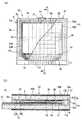
液晶装置12は、液晶Lを挟んで対向する前面側基板(第1の基板)1aと背面側基板(第2の基板)1bとを、これら2枚の基板の周縁部に環状に設けたシール材6aによって接着一体化したものである。観察側に配置された前面側基板1aには、透光性材料からなる基板本体2aの液晶層側の面に、透光性の前面側電極3aや配向膜4a等からなる液晶配向制御層が形成されており、観察側とは反対側に配置された背面側基板1bには、透光性材料からなる基板本体2bの液晶層側の面に、透光性の背面側電極3bや配向膜4b等からなる液晶配向制御層が形成されている。2枚の基板1a,1bのギャップは、スペーサ10aによって均一に保持されている。この液晶装置12は、パッシブマトリクス型又はアクティブマトリクス型のいずれであってもよく、液晶の配向形態も、TN型、VAN型、STN型、強誘電型、反強誘電型等の種々の公知の形態を採り得る。また、背面側基板22bに反射膜を形成して反射型の液晶表示装置を構成してもよく、更に、この反射膜に開口部やスリット等の透光部を形成して、半透過反射型の液晶表示装置を構成することも可能である。本実施形態では、液晶装置12は単純マトリクス型の液晶装置とされており、前面側基板1a及び背面側基板1bの各電極3a,3bは、それぞれ図1(a)において図示左右方向及び図示上下方向に延在するストライプ状の電極として形成されている。図1(a)において、前面側電極3aと背面側電極3bとの各交差領域がそれぞれ1つのドットを構成し、これらドットの集まりによって表示領域が形成されている。 The
また、本実施形態の液晶装置12には、前面側基板1aの基板本体2aと前面側電極3aとの間にカラーフィルタ21が設けられている。このカラーフィルタ21には、各ドットに対応して複数の着色層(図示略)が設けられており、これらの着色層の表面には必要に応じて保護膜であるオーバーコート層(図示略)が設けられている。このカラーフィルタ21は、シール材付近での基板の段差をなくすために、シール材6aの内側の表示領域からシール材6aの外側の額縁領域に延設されている。 In the
前面側基板1aには、背面側基板1bの外周側に張り出した張り出し部1cが設けられている。この張り出し部1cは実装端子形成領域として使用するものである。前面側基板1aの前面側電極3aは張り出し部1cに向けて伸び、端子13の一部を構成している。また、背面側基板1bの背面側電極3bは、シール材6aに混入された導通材14を介して前面側基板1aの配線16に導電接続されており、配線16は張り出し部1cの端子13に接続されている。端子13は、張り出し部1cに実装される液晶駆動用IC(図示略)との間の電気的な接続をとるための配線パターンであり、本実施形態では、この端子13に液晶駆動用ICがFPC実装されるようになっている。なお、実装形態としてはCOG実装等の他の形態を採用することも可能である。
このように構成された液晶装置12の上下の面(即ち、液晶装置12の前面側基板1aの観察側の面、及び液晶装置12の背面側基板1bの観察側とは反対側の面)には、それぞれ前面側偏光板17a及び背面側偏光板17bが配置されている。The
On the upper and lower surfaces of the
ところで、本実施形態の液晶装置12には、基板1a,1b間のギャップと略同じ高さを有する隔壁10(図1(a)において斜めハッチングが施された部分)が背面側基板1bの外周の縁に沿って額縁状に形成されている。この隔壁10には背面側基板1bの外周に沿う環状の溝Hが形成されており、隔壁10はこの溝Hを挟んで内周側に配置される内壁部(第1の環状の隔壁部)10Bと外周側に配置される外壁部(第2の環状の隔壁部)10Aとに分割されている。前述のシール材6aはこの隔壁10の溝内に充填されており、シール材6aの外周は外壁部10Aによって外気から隔離され、シール材6aの内周は内壁部10Bによって液晶から隔離された状態になっている。この隔壁10の内壁部10B及び外壁部10Aの幅はミクロンオーダーの微細な幅に設定されており、シール材6aはその内周及び外周が隔壁10の溝の内面に接する状態に形成されている。すなわち、本実施形態において、シール材6aは背面側基板1bの端縁ぎりぎりのところに形成されており、背面側基板1bのシール材6aの外側には無駄な額縁領域が殆どない状態となっている(なお、図1では図面の都合上、額縁領域を広く描いている)。この隔壁10は、液晶装置12の製造過程においてはシール材6aの幅方向の流動を堰き止めるための土手として機能し、製造後においてはシール材6aと共に外部の湿気等を遮断するためのガスバリア層として機能するものである。 By the way, in the
[液晶装置の製造方法]
次に、本実施形態の液晶装置12の製造方法について説明する。
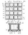
図2は、液晶装置12の製造工程を示すフローである。本実施形態では、大面積のマザー基板を用いて複数の液晶装置を一括して形成し、切断によって個々の液晶装置12に分離する方法を採用する。図2に示す液晶装置の製造方法においては、工程P1から工程P5に至る一連の工程によって図3に示す大判の前面側マザー基板(第1のマザー基板)101aが形成され、工程P11から工程P13に至る一連の工程によって図4に示す大判の背面側マザー基板(第2のマザー基板)101bが形成される。なお、前面側マザー基板101aは、前面側基板1aとなる複数の矩形の基板領域(図3においてスクライブ線G1,G4によって囲まれる領域)を含む大判の基板であり、背面側マザー基板101bは、背面側基板1bとなる複数の矩形の基板領域(図4においてスクライブ線G2,G3,G4によって囲まれる領域)を含む大判の基板である。[Method of manufacturing liquid crystal device]
Next, a method for manufacturing the
FIG. 2 is a flow showing the manufacturing process of the
まず、図3を用いて前面側マザー基板101aの形成工程(工程P1〜工程P5)について説明する。
ここでは、まず、工程P1において、ガラスやプラスチック等の透光性材料からなる大判の第1基材102aの表面に液晶装置複数分のカラーフィルタ21を形成する。カラーフィルタ21は、各基板領域の表示領域と額縁領域(シール材6aから背面側基板1bの縁が配置される部分までの領域)の双方に形成する。前述のように本実施形態では液晶装置12の側面をシール材6aと隔壁10の外壁部10Aによって二重に封止しているが、この隔壁10は後述のように表示領域内のスペーサ10aと共通の工程によって一括的に形成されるので、表示領域とシール材6aの外側領域との間でギャップが異なると隔壁10の高さが足りなくなり、シール材6aの上部が露出してしまう可能性がある。このため、本実施形態ではシール材6aの外側にカラーフィルタ21を延設することによって表示領域と額縁領域との間の凹凸をなくし、基板101a,101bの隙間が隔壁10によって確実に埋められるようにしている。なお、カラーフィルタ21を延設する代わりに、シール材6aの外側にギャップ調整用の層(ギャップ調整層)を別部材で形成してもよい。
次に、第1基材102aの表面に液晶装置複数分の前面側電極3a及び配線16等を形成する。前面側電極3a及び配線16は、第1基材102aの表面全体にITO等の透光性導電膜をスパッタし、これをエッチングすることによって、各基板領域に対して一括的に形成することができる。First, the formation process (process P1-process P5) of the front side mother board |
Here, first, in the process P1, the
Next, a plurality of
次に、工程P2において、第1基材102aの表面にギャップ制御用のスペーサ10a及び隔壁10を形成する。スペーサ10aは、各基板領域の表示領域となる部分、及びシール材6aの液晶注入口18が形成される部分に形成する。隔壁10は、背面側マザー基板101bの各基板領域の境界部、即ち、背面側基板1bの4つの縁辺(液晶注入口18を除く基板の上辺、端子部13の形成される基板の下辺、及びスクライブ線G4に沿う基板の左右の辺)が配置される位置に連続的に形成する。この際、スクライブ線G4を挟んで近接する左右の基板領域の隔壁10は繋げてもよいし僅かに離間させてもよい。本実施形態では、この左右の隔壁10を繋げて(即ち、スクライブ線G4を挟んで連続的に)形成するものとする。この隔壁10にはシール材6aを収容するための溝Hを形成し、この溝Hによって隔壁10を2つの環状の隔壁部(内壁部10B及び外壁部10A)に分割する。これらの要素は、感光性樹脂等のパターニングによって一括して形成することができるが、これらを別部材によって別工程で形成することも可能である。 Next, in step P2, a
本実施形態において隔壁10は、隣接する基板領域を仕切るための仕切り壁であって、後述の工程P21において基板101a,101bを貼り合わせる際のシール材6aの土手として機能するものである。工程P21の基板の貼り合わせ工程では、工程P5で塗布されたシール材6aがつぶされて左右に広がるため、他の基板領域のシール材との干渉(特に、スクライブ線G4を挟んで隣り合う基板領域の間でのシール材6a,6aの干渉)やシール材と表示領域との干渉を避けるために、従来はシール材6aとシール材6aとの間隔及びシール材6aと表示領域との間隔をこのつぶれ分のマージンを考慮して広めにとっていた。しかし、このようなマージン部分は無駄な領域となるので、できるだけ少なくすることが望ましい。本実施形態では、このような問題をシール材6aの両側に隔壁10を配置することによって解決している。すなわち、シール材6aの両側に隔壁10を配置した場合には、シール材6aがつぶれたときにシール材6aの幅方向の流れ(即ち、隣の基板領域に向かう流れと基板領域の内側に向かう流れ)が隔壁10によって堰き止められるので、隣接する基板領域の間でシール材同士が干渉したり、シール材6aが表示領域内に入り込んだりすることはない。また、シール材6aの幅を隔壁10の溝Hの幅に正確に規定できるので、シール材6aの塗布量のばらつきを考慮する必要がなくなる。このため、従来よりも表示領域を相対的に広くとることができ、又、基板領域の間隔を狭くしてこれらを密に配置することが可能になる。このように隔壁10はシール材6aとシール材6aの間を仕切ることができればよいので、隔壁10の幅はさほど広くする必要はなく、むしろ一定の強度(例えばシール材6aの流動圧力に対抗しうる強度)を保てる範囲で隔壁10の幅をできるだけ狭くして無駄な額縁領域をなくすことが望ましい。 In the present embodiment, the
次に、工程P3において、第1基材102aの各基板領域に配向膜4aを形成し、さらに工程P4において、配向膜4aに対してラビング処理を実行する。配向膜4aは、例えばポリイミドを塗布又は印刷することによって形成することができる。 Next, in step P3, an
次に、工程P5において、各基板領域の周縁部にエポキシ樹脂等からなるシール材6aを矩形枠状に形成する。このシール材6aは、ディスペンサを用いて隔壁10の溝H内に正確に配置する。このシール材6aには液晶注入口18を形成する。この液晶注入口18は、後述の工程P23(図5,図6)において1列分のパネル構造体7(図5参照)に対して液晶を一括して注入できるように、スクライブ線G1に沿う基板領域の縁辺に設けるものとする。なお、シール材6aには、第2基材102bの背面側電極3bを第1基材102aの配線16に導通させるための導通材14(金属微粒子等)を練り込んでおく。
以上により、液晶装置複数分のパターンが形成された大判の前面側マザー基板101aが作製される。なお、前面側マザー基板101a上には、必要に応じて、カラーフィルタ21,前面側電極3a,配向膜4a,スペーサ10a,隔壁10以外の光学的要素が形成されることもあるが、図3ではそれら付加的な光学的要素は省略してある。Next, in step P5, a sealing
Thus, a large front-
次に、図4を用いて背面側マザー基板101bの形成工程(工程P11〜P13)について説明する。
ここでは、まず、工程P11において、ガラスやプラスチック等の透光性材料からなる大判の第2基材102bの表面に、液晶装置複数分の背面側電極3bを形成する。背面側電極3bは、第2基材102bの表面全体にITO等の透光性導電膜をスパッタし、これをエッチングすることによって、各基板領域に対して一括的に形成することができる。なお、図4では、第2基材102bを通して背面側電極3bを見た状態を示しており、さらに、第2基材102bは鎖線で仮想的に示してある。
次に、工程P12において、各基板領域内にポリイミド等からなる配向膜4bを形成し、さらに工程P13において、配向膜4bに対してラビング処理を実行する。
以上により、液晶装置複数分のパターンが形成された大判の背面側マザー基板101bが作製される。なお、背面側マザー基板101b上には、必要に応じて、背面側電極3b及び配向膜4b以外の光学的要素が形成されることもあるが、図4ではそれら付加的な光学的要素は省略してある。Next, the formation process (process P11-P13) of the back side mother board |
Here, first, in the process P11, the back-
Next, in step P12, an
In this way, a large back-
前面側マザー基板101a及び背面側マザー基板101bが形成されたら、図2の工程P21において、両基板101a,101bをシール材6aによって貼り合わせ、液晶装置複数分の空セルを有した大判のパネル構造体を形成する。前述のようにシール材6aは隔壁10の溝内に配置されているので、基板101a,101bを圧着してシール材6aをつぶしたときに、隔壁10の内壁部10B及び外壁部10Aが土手となってシール材6aの幅方向の流れが堰き止められる。このため、基板領域の間隔やシール材と表示領域との間隔を従来よりも狭くしているにも拘わらず、隣り合うシール材の間で干渉が生じたり、シール材が表示領域内に入り込んだりすることはない。 After the
次に、工程P22において、図3に示すスクライブ線G1に沿って第1基材102a上にスクライブ用の溝を形成し、さらに図4に示すスクライブ線G2,G3に沿って第2基材102b上にスクライブ用の溝を形成する。そして、これらの溝に従ってパネル構造体を切断することにより、図5に示すような1列分のパネル構造体、いわゆる短冊状のパネル構造体7を形成する。この短冊状のパネル構造体7においては、シール材6aに形成した液晶注入口18の一部が外部に露出した状態となっている。なお、図5においては、切断後の前面側マザー基板101a及び背面側マザー基板101bをそれぞれ符号111a及び符号111bで示し、切断後の第1基材102a及び第2基材102bをそれぞれ符号112a及び符号112bで示している。 Next, in step P22, a scribe groove is formed on the
次に、工程P23において液晶の注入を行なう。具体的には、まず、図6に示すように、液晶L0を収容した容器8と短冊状のパネル構造体7とを密閉チャンバ9内に入れる。そして、密閉チャンバ9内を減圧(例えば真空状態に減圧)することにより、パネル構造体7内の各シール材6aの内側の領域を減圧し、この状態でパネル構造体7の各液晶装置部分の液晶注入口18を液晶L0の液面に漬ける。その後、密閉チャンバ9内の減圧状態を大気圧に戻すことにより、液晶L0の液面に大気圧を加え、これにより、液晶注入口18を通してシール材6aの内部に液晶L0を注入する。その後、各シール材6aの液晶注入口18をエポキシ樹脂等の封止材11(図1(a)参照)によって封止する。このような封止材は硬化収縮によって液晶注入口付近のギャップを変形させることが知られているが、本実施形態ではスペーサ10aを液晶注入口18に配置しているので、このようなギャップむらは発生しない。 Next, liquid crystal is injected in Step P23. Specifically, first, as shown in FIG. 6, the
次に、工程P24において、図5のスクライブ線G4にそって第1基材112a及び第2基材112b上にスクライブ用の溝を形成する。そして、これらの溝に従ってパネル構造体7を切断して個々のパネルに分離し、工程P25において、各パネルの洗浄を行なう。具体的には、界面活性剤を混入させた洗浄液をパネルの表面に供給し、液晶注入口付近に付着した液晶L0の残りかすを除去する。次に、工程P26において、各パネルの前面側基板1a及び背面側基板1bの外側表面に偏光板17a,17b(図1(b)参照)を貼着する。続いて、工程P27において、前面側基板1aの張出し部1cに形成した端子13に、例えばFPC(Flexible Printed Circuit)等を介して液晶駆動用ICを実装する。
以上により、液晶装置12が完成する。Next, in step P24, scribe grooves are formed on the
Thus, the
以上説明したように、本実施形態ではシール材の内側と外側を隔壁で仕切った状態でマザー基板101a,101bの貼り合わせを行なっているので、シール材が両側の隔壁を越えて他の領域に広がることはない。また、隣り合うシール材6aとシール材6aとの間隔及びシール材と表示領域との間隔が、これらの境界部に設置された隔壁10の幅によって正確に規定されるので、例えばこの隔壁10をフォトリソグラフィ技術を用いて微細な幅に形成すれば、表示に寄与しない無駄な領域を実質的になくすことができる。 As described above, in the present embodiment, the
また、本実施形態では液晶装置12の側面がシール材6aと隔壁10によって二重に封止された状態になるので、外部からの湿気等の侵入を確実に防止することができ、更に、液晶とシール材が隔離されているので、シール材から溶出した不純物によって液晶が汚染されることがない。また、この構造においては、隔壁10によって十分なガスバリア性が確保される場合には、接着力が損なわれない範囲でシール幅を最大限細くする(例えば0.1mm幅)ことによって、液晶装置12を更に狭額縁化することもできる。 In the present embodiment, the side surface of the
[第2の実施の形態]
[液晶装置の製造方法]
次に、本発明の第2の実施形態に係る液晶装置の製造方法について説明する。なお、本実施形態において前記第1の実施形態と同様の部材又は部位については同じ符号を付し、詳細な説明は省略する。[Second Embodiment]
[Method of manufacturing liquid crystal device]
Next, a method for manufacturing a liquid crystal device according to the second embodiment of the present invention will be described. In addition, in this embodiment, the same code | symbol is attached | subjected about the member or site | part similar to the said 1st Embodiment, and detailed description is abbreviate | omitted.
図7は、本実施形態の液晶装置の製造工程を示すフローである。本実施形態では、液晶をマザー基板上に塗布し、マザー基板の貼り合わせと同時に液晶の充填を行なう方法を採用する。図7に示す液晶装置の製造方法においては、工程P1から工程P6に至る一連の工程によって図8に示す大判の前面側マザー基板(第1のマザー基板)101aが形成され、工程P11から工程P13に至る一連の工程によって図4に示した大判の背面側マザー基板(第2のマザー基板)101bが形成される。なお、背面側マザー基板101bに関しては前記第1の実施形態と同様であるので、ここでは説明を省略する。 FIG. 7 is a flow showing the manufacturing process of the liquid crystal device of the present embodiment. In the present embodiment, a method is adopted in which liquid crystal is applied onto a mother substrate and the liquid crystal is filled simultaneously with the bonding of the mother substrate. In the method of manufacturing the liquid crystal device shown in FIG. 7, a large front-side mother substrate (first mother substrate) 101a shown in FIG. 8 is formed by a series of steps from step P1 to step P6, and steps P11 to P13 are performed. The large-sized back side mother board (second mother board) 101b shown in FIG. Note that the back-
前面側マザー基板101aの製造に当たっては、まず、工程P1において、ガラスやプラスチック等の透光性材料からなる大判の第1基材102aの表面に液晶装置複数分のカラーフィルタ21,前面側電極3a,配線16等を形成する。カラーフィルタ21は、各基板領域の表示領域と額縁領域(シール材6aから背面側基板1bの縁が配置される部分までの領域)の双方に形成する。 In manufacturing the front-
次に、工程P2において、第1基材102aの表面にギャップ制御用のスペーサ10a及び隔壁10を形成する。スペーサ10aは、各基板領域の表示領域となる部分に形成する。隔壁10は、背面側マザー基板101bの各基板領域の境界部、即ち、背面側基板1bの4つの縁辺が配置される位置に連続的に形成する。この隔壁10にはシール材6aを収容するための溝Hを形成し、この溝Hによって、隔壁10を2つの環状の隔壁部(内壁部10B及び外壁部10A)に分割する。これらの要素は、感光性樹脂等のパターニングによって一括して形成することができるが、これらを別部材によって別工程で形成することも可能である。 Next, in step P2, a
ところで、本実施形態では、液晶をマザー基板の貼り合わせによって充填するため、シール材6aには液晶注入口を設ける必要がない。このため、隔壁10及びシール材6aは閉環状に形成することになる。後述のように、本実施形態ではシール材6aをディスペンサによって一筆書きで描画するが、この場合、シール材の切れ目をなくすために描画の開始点と終了点はオーバーラップさせて形成するので、開始点付近(即ち、終了点付近)のシール材の塗布量が多くなってしまい、マザー基板を貼り合わせたときに、この部分のシール材の広がりが他の部分よりも大きくなってしまうという問題があった。本実施形態では、このような塗布量のばらつきはシール材6aが溝内を流動することによってある程度平均化されるが、ばらつきが大きいとシール材6aが溝Hから溢れて表示領域内に入り込んだり、隣の基板領域との間で干渉が生じたりする虞がある。そこで、本実施形態では、図8の部分拡大図に示すように、描画の開始位置に対応する部分(本実施形態では基板の右上隅に設定している)の隔壁の溝H′(シール溜り)の幅を他の部分の溝Hの幅よりも広くし、余剰なシール材6aが溝から溢れないようにしている。なお、シール溜りH′(即ち、ディスペンサによる塗布の開始点)を基板の角部に設定したのは、ここが他の部分(例えば基板の縁辺中央部)に比べてスペース的に余裕があるためであるが、シール溜りH′の位置は必ずしもここに限定されるものではない。 By the way, in this embodiment, since the liquid crystal is filled by bonding the mother substrate, it is not necessary to provide a liquid crystal injection port in the sealing
次に、工程P3において、第1基材102aの各基板領域に配向膜4aを形成し、さらに工程P4において、配向膜4aに対してラビング処理を実行する。配向膜4aは、例えばポリイミドを塗布又は印刷することによって形成することができる。 Next, in step P3, an
次に、工程P5において、各基板領域の周縁部にエポキシ樹脂等からなるシール材6aを矩形枠状に形成する。このシール材6aは、ディスペンサを用いて隔壁10の溝H内に正確に配置する。本実施形態では、シール材6aに液晶注入口を形成しないので、シール材6aは各基板領域の角部を開始点として一筆書きで閉環状に形成される。この場合、塗布の開始点と終了点はオーバーラップするのでこの部分の塗布量は多くなるが、この塗布開始点の隔壁の溝は前述したように幅広に形成されているので、基板の貼り合わせ工程において余剰なシール材6aが溝から溢れることはない。 Next, in step P5, a sealing
次に、工程P6において、各基板領域のシール枠内(即ち、内壁10Bの内側の領域)に液晶を塗布する。図9(a)は、液晶の塗布方法の一例を示す図である。本実施形態では、インクジェットヘッド500を用いて液晶Lを液滴状にして吐出し、これを基板表面に連続的に多数配置することによって所定の広さを持った液膜を形成する。本工程では、このような液膜を各基板領域に順次形成していく。液膜が形成されたら、工程P21において、両基板101a,101bをシール材6aによって貼り合わせ、図9(b)に示す液晶装置複数分の大判のパネル構造体7′を形成する。前述のようにシール材6aは隔壁10の溝内に配置されているので、基板101a,101bを圧着してシール材6aをつぶしたときに、隔壁10の内壁部10B及び外壁部10Aが土手となってシール材6aの幅方向の流れが堰き止められ、隣の基板領域や表示領域等に広がることはない。また、液晶Lとシール材6aは内壁部10Bによって隔離されているため、未硬化のシール成分によって液晶Lが汚染されることもない。 Next, in process P6, liquid crystal is applied in the seal frame of each substrate region (that is, the region inside the
次に、工程P22において、図8に示すスクライブ線G1に沿って第1基材102a上にスクライブ用の溝を形成し、さらに図4に示すスクライブ線G2,G3に沿って第2基材102b上にスクライブ用の溝を形成する。そして、これらの溝に従ってパネル構造体を切断し、個々のパネルに分離する。そして、工程P25において、各パネルの洗浄を行ない、工程P26において、各パネルの前面側基板1a及び背面側基板1bの外側表面に偏光板17a,17b(図1(b)参照)を貼着する。続いて、工程P27において、前面側基板1aの張出し部1cに形成した端子13に、例えばFPC(Flexible Printed Circuit)等を介して液晶駆動用ICを実装する。
以上により、液晶装置が完成する。Next, in step P22, a scribe groove is formed on the
Thus, the liquid crystal device is completed.
以上説明したように、本実施形態では液晶をマザー基板の貼り合わせによって充填するため、真空注入を行なう場合に比べて工程を簡略化することができる。このような方法では、未硬化のシール材と液晶とが接触することによって液晶が汚染されることが問題となるが、本実施形態では液晶とシール材とを隔壁10によって隔離しているので、液晶内に直接シール材の未硬化成分が溶出することはない。 As described above, in the present embodiment, since the liquid crystal is filled by bonding the mother substrate, the process can be simplified as compared with the case where vacuum injection is performed. In such a method, there is a problem that the liquid crystal is contaminated by contact between the uncured sealing material and the liquid crystal, but in the present embodiment, the liquid crystal and the sealing material are separated by the
なお、本実施形態では、シール溜りH′の容積を大きくするためにシール溜りH′における溝の幅を他の部分よりも広くしたが、この代わりにシール溜りH′の溝の深さを他の部分よりも深くすることによっても同様の効果を得ることができる。具体的には、ディスペンサの塗布開始点以外の溝Hの深さを図10(a)のように隔壁10の厚みよりも浅くし、塗布開始点の溝H′の深さを図10(b)のように隔壁10の厚みと同じとする構成が考えられる。前述のように、本実施形態ではマザー基板の無駄を省くために隔壁10を各基板領域の端縁ぎりぎりのところに形成しているので、シール材6aを収容するための余剰なスペースを確保することは難しいが、図10の構成では、溝の幅は変えずに溝の深さを増やすことによって余剰なシール材を収容するので、マザー基板に無駄ができることはない。 In this embodiment, in order to increase the volume of the seal reservoir H ′, the width of the groove in the seal reservoir H ′ is made wider than that of other portions. The same effect can be obtained by making it deeper than the part. Specifically, the depth of the groove H other than the application start point of the dispenser is made shallower than the thickness of the
[電子機器]
次に、本発明の液晶装置を備えた電子機器の具体例について説明する。
図11は、携帯電話の一例を示した斜視図である。図11において、符号1000は携帯電話本体を示し、符号1001は前記実施形態の液晶装置を用いた表示部を示している。このような携帯電話等の電子機器の表示部に本発明の液晶装置を用いた場合、高温・高湿下で信頼性が高く狭額縁な液晶表示部を備えた電子機器を実現することができる。
なお、本発明の液晶装置は、前述した携帯電話機に限らず、種々の電子機器に搭載することができる。この電子機器としては例えば、電子ブック、パーソナルコンピュータ、ディジタルスチルカメラ、液晶テレビ、ビューファインダ型あるいはモニタ直視型のビデオテープレコーダ、カーナビゲーション装置、ページャ、電子手帳、電卓、ワードプロセッサ、ワークステーション、テレビ電話、POS端末、タッチパネルを備えた機器等があり、前記液晶装置はこれらの画像表示手段として好適に用いることができる。[Electronics]
Next, specific examples of an electronic device including the liquid crystal device of the present invention will be described.
FIG. 11 is a perspective view showing an example of a mobile phone. In FIG. 11,
Note that the liquid crystal device of the present invention is not limited to the mobile phone described above, and can be mounted on various electronic devices. Examples of the electronic apparatus include an electronic book, a personal computer, a digital still camera, a liquid crystal television, a viewfinder type or a monitor direct-view type video tape recorder, a car navigation device, a pager, an electronic notebook, a calculator, a word processor, a workstation, and a video phone. , A POS terminal, a device equipped with a touch panel, etc., and the liquid crystal device can be suitably used as these image display means.
以上、添付図面を参照しながら本発明に係る好適な実施の形態例について説明したが、本発明は係る例に限定されないことは言うまでもない。上述した例において示した各構成部材の諸形状や組み合わせ等は一例であって、本発明の主旨から逸脱しない範囲において設計要求等に基づき種々変更可能である。
例えば、前記実施形態では隔壁10を背面側マザー基板1bの各基板領域の縁辺となる位置に環状に形成したが、隔壁10は少なくとも各基板領域が近接して配置される部分(即ち、シール材同士が干渉しやすくなる部分。例えば図3においてスクライブ線G4に沿う基板領域の左右の縁辺)に形成されていればよく、必ずしも全ての縁辺に形成する必要はない。また、前記実施形態では隔壁10を前面側マザー基板101aに形成したが、隔壁10は背面側マザー基板101bに形成してもよいし、前面側マザー基板101aと背面側マザー基板101bの両方に形成してもよい。同様に、シール材6aは背面側マザー基板101bに形成してもよいし、前面側マザー基板と背面側マザー基板の両方に形成してもよい。The preferred embodiments of the present invention have been described above with reference to the accompanying drawings, but it goes without saying that the present invention is not limited to such examples. Various shapes, combinations, and the like of the constituent members shown in the above-described examples are examples, and various modifications can be made based on design requirements and the like without departing from the gist of the present invention.
For example, in the above-described embodiment, the
また、前記実施形態では液晶装置12を大判のマザー基板を用いて多面取りで形成する方法を示したが、液晶装置12は枚葉の基板を用いて形成することもできる。この場合でも、前述したのと同様の方法で製造することができる。すなわち、この場合にはまず、液晶パネルを構成する一対の基板(即ち、前面側基板1aと背面側基板1b)のうちいずれか一方の基板に対して、前記基板の表示領域となる部分のギャップを規定するためのスペーサと、前記表示領域となる部分の縁辺に沿う環状の隔壁であって前記表示領域となる部分の外周に沿う環状の溝を有する前記ギャップと略同じ高さの隔壁とを同一の材料によって一括で形成する。次に、これら一対の基板の少なくとも一方に対して前記隔壁の溝の配置される位置に環状のシール材を形成し、このシール材を介して前記一対の基板を貼り合わせる。この場合にも、前述したのと同様の効果が得られる。
また、前記実施形態では、本発明を単純マトリクス型の液晶装置に適用したが、本発明は、その他の任意の構造の液晶装置、例えばTFD素子等の二端子型非線形素子或いはTFT素子等の三端子型非線形素子を用いるアクティブマトリクス型の液晶装置にも適用可能である。In the above-described embodiment, the method of forming the
In the above embodiment, the present invention is applied to a simple matrix type liquid crystal device. However, the present invention is not limited to a liquid crystal device having any other structure, for example, a two-terminal nonlinear element such as a TFD element or a TFT element. The present invention can also be applied to an active matrix liquid crystal device using a terminal-type nonlinear element.
1a…前面側基板(第1の基板)、1b…背面側基板(第2の基板)、6a…シール材、10…隔壁、10a…スペーサ、12…液晶装置、18…液晶注入口、101a,111a…前面側マザー基板(第1のマザー基板)、101b,111b…背面側マザー基板(第2のマザー基板)、1000…電子機器、H,H′…溝、L…液晶
DESCRIPTION OF
Claims (16)
Translated fromJapanese前記一対の基板の少なくとも一方に対して、前記基板の表示領域となる部分のギャップを規定するためのスペーサと、前記表示領域となる部分の縁辺に沿う環状の隔壁であって前記表示領域となる部分の外周に沿う環状の溝を有する前記ギャップと略同じ高さの隔壁とを同一の材料によって一括で形成する工程と、
前記一対の基板の少なくとも一方に対して、前記隔壁の溝の配置される位置に環状のシール材を形成する工程と、
前記一対の基板を前記シール材を介して貼り合わせる工程とを備えたことを特徴とする、液晶装置の製造方法。A method of manufacturing a liquid crystal device in which a liquid crystal is sandwiched between a pair of opposing substrates,
A spacer for defining a gap of a portion to be a display region of the substrate with respect to at least one of the pair of substrates, and an annular partition along an edge of the portion to be the display region, which serves as the display region A step of collectively forming the gap having an annular groove along the outer periphery of the portion and a partition wall having substantially the same height with the same material;
Forming an annular sealing material at a position where the groove of the partition wall is disposed with respect to at least one of the pair of substrates;
A method for manufacturing a liquid crystal device, comprising: bonding the pair of substrates through the sealing material.
前記一対の基板の一方の基板となる複数の基板領域を含むマザー基板と、前記一対の基板の他方の基板となる複数の基板領域を含むマザー基板とを用意し、これら2枚のマザー基板の少なくとも一方に対して、前記基板領域の表示領域となる部分のギャップを規定するためのスペーサと、前記表示領域となる部分の縁辺に沿う環状の隔壁であって前記表示領域となる部分の外周に沿う環状の溝を有する前記ギャップと略同じ高さの隔壁とを同一の材料によって一括で形成する工程と、
前記2枚のマザー基板の少なくとも一方に対して、前記隔壁の溝の配置される位置に環状のシール材を形成する工程と、
前記2枚のマザー基板を前記シール材を介して貼り合わせる工程と、
前記2枚のマザー基板を切断して個々の液晶装置に分離する工程とを備えたことを特徴とする、液晶装置の製造方法。A method of manufacturing a liquid crystal device in which a liquid crystal is sandwiched between a pair of opposing substrates,
A mother substrate including a plurality of substrate regions serving as one substrate of the pair of substrates and a mother substrate including a plurality of substrate regions serving as the other substrate of the pair of substrates are prepared. At least one of the spacer for defining the gap of the part that becomes the display area of the substrate area and an annular partition wall along the edge of the part that becomes the display area, and on the outer periphery of the part that becomes the display area A step of collectively forming a partition having substantially the same height as the gap having an annular groove along the same material;
Forming an annular sealing material at a position where the groove of the partition wall is disposed with respect to at least one of the two mother substrates;
Bonding the two mother substrates through the sealing material;
And a step of cutting the two mother substrates and separating them into individual liquid crystal devices.
前記一対の基板の表示領域となる部分のギャップを規定するためのスペーサと、前記表示領域の外周に沿って配置された環状の隔壁であって前記スペーサと同一の材料によって形成された前記ギャップと略同じ高さの隔壁と、前記一対の基板を接着するためのシール材とを備え、
前記隔壁が前記表示領域の外周に沿って配置される環状の溝を有し、前記シール材が前記隔壁の溝内に配置されていることを特徴とする、液晶装置。A liquid crystal device having a liquid crystal sandwiched between a pair of opposing substrates,
A spacer for defining a gap between portions of the pair of substrates serving as display areas; and an annular partition wall disposed along an outer periphery of the display area, the gap formed of the same material as the spacers; A partition having substantially the same height, and a sealing material for bonding the pair of substrates,
The liquid crystal device, wherein the partition wall has an annular groove disposed along an outer periphery of the display area, and the sealing material is disposed in the groove of the partition wall.
An electronic apparatus comprising the liquid crystal device according to claim 15.
Priority Applications (1)
| Application Number | Priority Date | Filing Date | Title |
|---|---|---|---|
| JP2004206976AJP2006030439A (en) | 2004-07-14 | 2004-07-14 | Liquid crystal device, method for manufacturing liquid crystal device, and electronic apparatus |
Applications Claiming Priority (1)
| Application Number | Priority Date | Filing Date | Title |
|---|---|---|---|
| JP2004206976AJP2006030439A (en) | 2004-07-14 | 2004-07-14 | Liquid crystal device, method for manufacturing liquid crystal device, and electronic apparatus |
Publications (1)
| Publication Number | Publication Date |
|---|---|
| JP2006030439Atrue JP2006030439A (en) | 2006-02-02 |
Family
ID=35896896
Family Applications (1)
| Application Number | Title | Priority Date | Filing Date |
|---|---|---|---|
| JP2004206976AWithdrawnJP2006030439A (en) | 2004-07-14 | 2004-07-14 | Liquid crystal device, method for manufacturing liquid crystal device, and electronic apparatus |
Country Status (1)
| Country | Link |
|---|---|
| JP (1) | JP2006030439A (en) |
Cited By (11)
| Publication number | Priority date | Publication date | Assignee | Title |
|---|---|---|---|---|
| JP2008015041A (en)* | 2006-07-03 | 2008-01-24 | Dainippon Printing Co Ltd | Alignment bonding apparatus and alignment bonding method |
| US7952680B2 (en) | 2008-07-08 | 2011-05-31 | Seiko Epson Corporation | Liquid crystal device and electronic apparatus |
| JP2011242656A (en)* | 2010-05-19 | 2011-12-01 | Toshiba Mobile Display Co Ltd | Liquid crystal display device and method for manufacturing the same |
| JP2012118268A (en)* | 2010-11-30 | 2012-06-21 | Toshiba Mobile Display Co Ltd | Liquid-crystal display panel |
| WO2013185372A1 (en)* | 2012-06-13 | 2013-12-19 | 深圳市华星光电技术有限公司 | Liquid crystal panel and producing method thereof |
| JP2014071437A (en)* | 2012-10-02 | 2014-04-21 | Japan Display Inc | Liquid crystal display device |
| US8717526B2 (en) | 2009-09-29 | 2014-05-06 | Japan Display Inc. | Liquid crystal display device and manufacturing method thereof |
| WO2014148187A1 (en)* | 2013-03-22 | 2014-09-25 | シャープ株式会社 | Display panel, and display panel manufacturing method |
| JP2014238444A (en)* | 2013-06-06 | 2014-12-18 | 株式会社ジャパンディスプレイ | Liquid crystal display device |
| TWI596412B (en)* | 2011-10-25 | 2017-08-21 | Japan Display Inc | Display device and method of manufacturing the same |
| WO2020008766A1 (en)* | 2018-07-04 | 2020-01-09 | ソニー株式会社 | Liquid crystal display element, production method for liquid crystal display element, and electronic device |
- 2004
- 2004-07-14JPJP2004206976Apatent/JP2006030439A/ennot_activeWithdrawn
Cited By (22)
| Publication number | Priority date | Publication date | Assignee | Title |
|---|---|---|---|---|
| JP2008015041A (en)* | 2006-07-03 | 2008-01-24 | Dainippon Printing Co Ltd | Alignment bonding apparatus and alignment bonding method |
| US7952680B2 (en) | 2008-07-08 | 2011-05-31 | Seiko Epson Corporation | Liquid crystal device and electronic apparatus |
| US8717526B2 (en) | 2009-09-29 | 2014-05-06 | Japan Display Inc. | Liquid crystal display device and manufacturing method thereof |
| US9013669B2 (en) | 2009-09-29 | 2015-04-21 | Japan Display Inc. | Liquid crystal display device and manufacturing method thereof |
| JP2011242656A (en)* | 2010-05-19 | 2011-12-01 | Toshiba Mobile Display Co Ltd | Liquid crystal display device and method for manufacturing the same |
| JP2012118268A (en)* | 2010-11-30 | 2012-06-21 | Toshiba Mobile Display Co Ltd | Liquid-crystal display panel |
| TWI596412B (en)* | 2011-10-25 | 2017-08-21 | Japan Display Inc | Display device and method of manufacturing the same |
| US9740052B2 (en) | 2011-10-25 | 2017-08-22 | Japan Display Inc. | Display device and method of manufacturing the same |
| WO2013185372A1 (en)* | 2012-06-13 | 2013-12-19 | 深圳市华星光电技术有限公司 | Liquid crystal panel and producing method thereof |
| JP2014071437A (en)* | 2012-10-02 | 2014-04-21 | Japan Display Inc | Liquid crystal display device |
| WO2014148187A1 (en)* | 2013-03-22 | 2014-09-25 | シャープ株式会社 | Display panel, and display panel manufacturing method |
| US9405155B2 (en) | 2013-06-06 | 2016-08-02 | Japan Display Inc. | Liquid crystal display device comprising a mounting portion located in a circumference area for mounting a signal source and method of manufacturing the same |
| JP2014238444A (en)* | 2013-06-06 | 2014-12-18 | 株式会社ジャパンディスプレイ | Liquid crystal display device |
| US9823523B2 (en) | 2013-06-06 | 2017-11-21 | Japan Display Inc. | Display device comprising a mounting portion located in a circumference area for mounting a signal source |
| US10359670B2 (en) | 2013-06-06 | 2019-07-23 | Japan Display Inc. | Display device comprising first and second insulating films having respective first and second concave portions facing each other |
| US10670925B2 (en) | 2013-06-06 | 2020-06-02 | Japan Display Inc. | Display device comprising a first insulating layer having a first concave portion formed between a resin layer and a pillar-shaped spacer |
| US11086169B2 (en) | 2013-06-06 | 2021-08-10 | Japan Display Inc. | Display device comprising a resin layer having a first width larger than a second width and an end surface of a seal material and an air gap overlap the resin layer |
| US11372277B2 (en) | 2013-06-06 | 2022-06-28 | Japan Display Inc. | Display device comprising first and second polarizing plates having ends located inside an end of a second substrate and an air gap between a resin layer and a second organic insulating film |
| US11614648B2 (en) | 2013-06-06 | 2023-03-28 | Japan Display Inc. | Display device comprising first and second polarizing plates having ends located inside an end of a second substrate and an air gap between a resin layer and an organic insulating film |
| US11841567B2 (en) | 2013-06-06 | 2023-12-12 | Japan Display Inc. | Display device comprising first and second polarizing plates having ends located inside an end of a second substrate and an air gap between a resin layer and the second substrate |
| WO2020008766A1 (en)* | 2018-07-04 | 2020-01-09 | ソニー株式会社 | Liquid crystal display element, production method for liquid crystal display element, and electronic device |
| JPWO2020008766A1 (en)* | 2018-07-04 | 2021-07-08 | ソニーグループ株式会社 | Liquid crystal display elements, manufacturing methods for liquid crystal display elements, and electronic devices |
Similar Documents
| Publication | Publication Date | Title |
|---|---|---|
| JP4841031B2 (en) | Manufacturing method of liquid crystal device | |
| JP4391928B2 (en) | Liquid crystal display device and manufacturing method thereof | |
| US20100182530A1 (en) | Display cell | |
| JP4532437B2 (en) | Liquid crystal display device and manufacturing method thereof | |
| JP2008165171A (en) | Liquid crystal display device and manufacturing method thereof | |
| JP2005202352A (en) | Liquid crystal panel and its manufacturing method | |
| JP2012226264A (en) | Liquid crystal display device and method of manufacturing the same | |
| KR20060063848A (en) | Manufacturing method of liquid crystal device | |
| CN1499267A (en) | Liquid crystal device, method of manufacturing liquid crystal device, and electronic device | |
| US20040207797A1 (en) | Electrooptical manufacturing apparatus, electrooptical apparatus, and electronic device | |
| JP2006030439A (en) | Liquid crystal device, method for manufacturing liquid crystal device, and electronic apparatus | |
| JP2004062038A (en) | Liquid crystal display | |
| WO2008072464A1 (en) | Liquid crystal display element | |
| KR100649413B1 (en) | Method and apparatus for discharging liquid crystal, liquid crystal device, manufacturing method thereof and electronic equipment | |
| JP2006030440A (en) | Liquid crystal device manufacturing method, liquid crystal device, and electronic apparatus | |
| JP2006208728A (en) | Liquid crystal display device and manufacturing method thereof | |
| JP2007193153A (en) | Electrooptical apparatus, method for manufacturing electrooptical apparatus, and electronic apparatus | |
| JP2008180935A (en) | Liquid crystal display panel and method for manufacturing liquid crystal display panel | |
| US9170459B2 (en) | Liquid crystal display device and manufacturing method thereof | |
| JP2003140178A (en) | Electro-optical device manufacturing method, electro-optical device, electronic apparatus, and ink jet type functional liquid ejection device | |
| JP5072525B2 (en) | Liquid crystal panel and manufacturing method thereof | |
| JP4368774B2 (en) | Liquid crystal display | |
| JP2007219300A (en) | Display device | |
| JP4720336B2 (en) | Electro-optical device manufacturing method and electro-optical device | |
| JP2002162913A (en) | Electro-optical device substrate unit, method of manufacturing electro-optical device substrate unit, electro-optical device, method of manufacturing electro-optical device, and electronic apparatus |
Legal Events
| Date | Code | Title | Description |
|---|---|---|---|
| A300 | Withdrawal of application because of no request for examination | Free format text:JAPANESE INTERMEDIATE CODE: A300 Effective date:20071002 |